Embed Size (px)
Citation preview
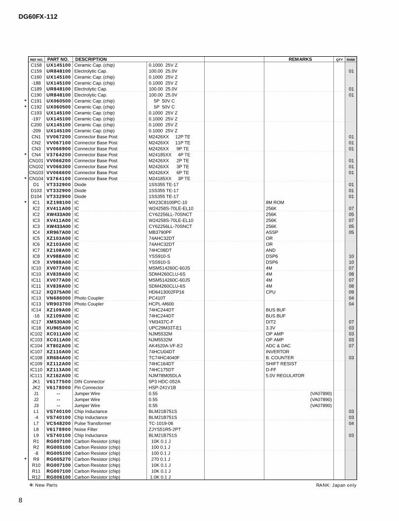
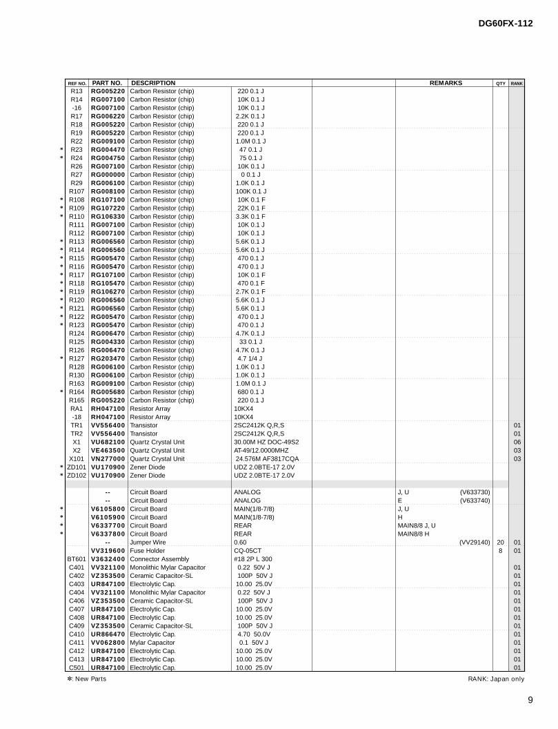
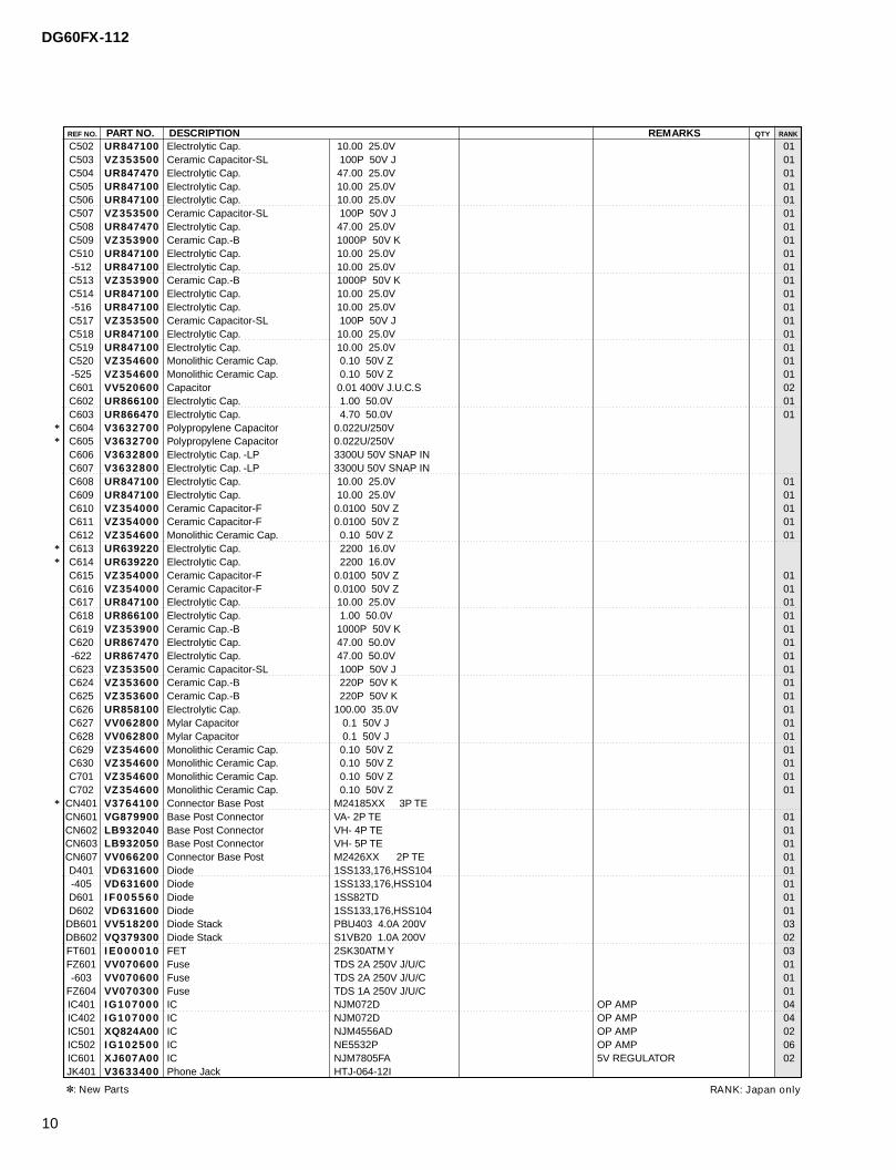
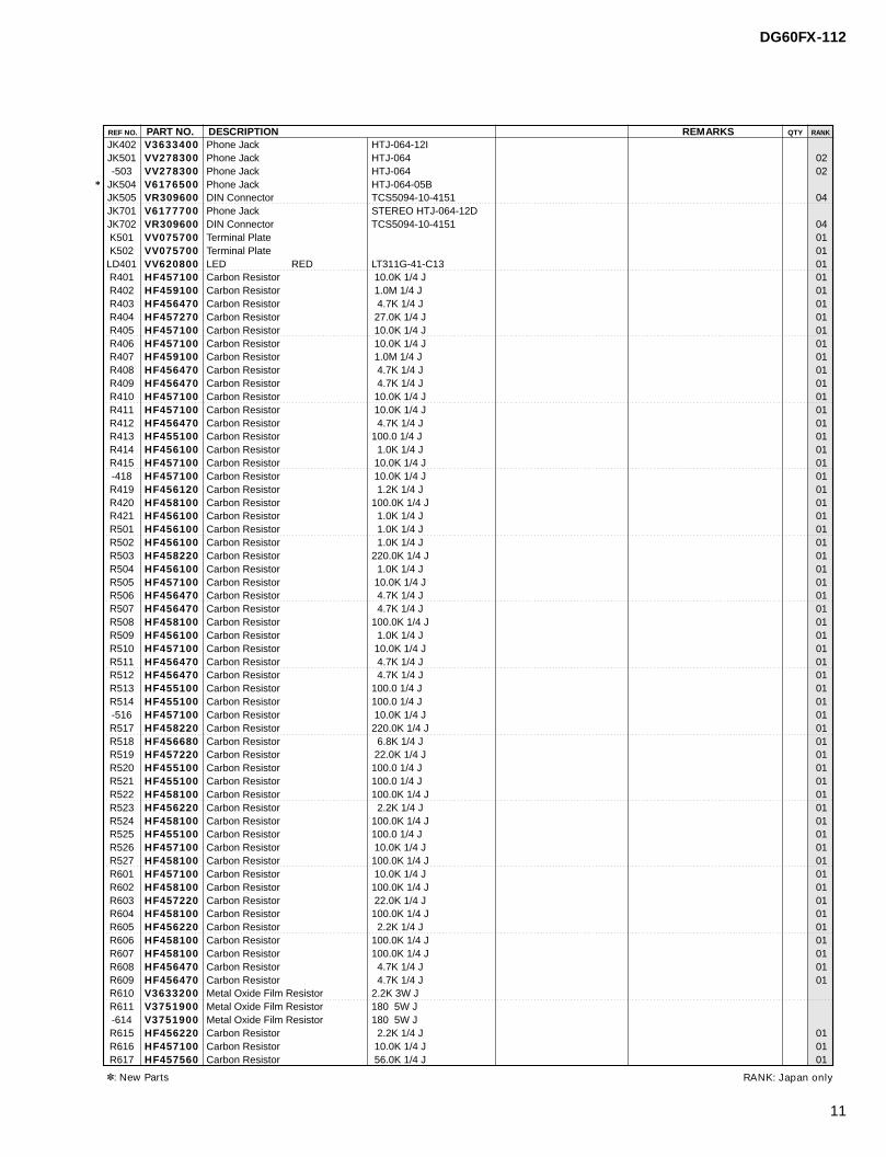
DG60FX-112
1
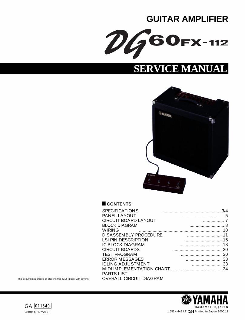
SERVICE MANUAL
GA 01154020001101-75000 1.552K-448 I.T Printed in Japan 2000.11
HAMAMATSU, JAPAN
GUITAR AMPLIFIER
CONTENTS
SPECIFICATIONS ................................................ 3/4PANEL LAYOUT .................................... 5CIRCUIT BOARD LAYOUT ................. 7BLOCK DIAGRAM ............................ 8WIRING ................................................................... 10DISASSEMBLY PROCEDURE ............................ 11LSI PIN DESCRIPTION .............................. 15IC BLOCK DIAGRAM ................................... 18CIRCUIT BOARDS ........................................ 20TEST PROGRAM ................................. 30ERROR MESSAGES ............................. 33IDLING ADJUSTMENT ........................ 33MIDI IMPLEMENTATION CHART ......................................... 34PARTS LISTOVERALL CIRCUIT DIAGRAMThis document is printed on chlorine free (ECF) paper with soy ink.
DG60FX-112
22
IMPORTANT NOTICEThis manual has been provided for the use of authorized Yamaha Retailers and their service personnel. It has been assumedthat basic service procedures inherent to the industry, and more specifically Yamaha Products, are already known and under-stood by the users, and have therefore not been restated.
WARNING : Failure to follow appropriate service and safety procedures when servicing this product may result in per-sonal injury, destruction of expensive components and failure of the product to perform as specified. Forthese reasons, we advise all Yamaha product owners that all service required should be performed by anauthorized Yamaha Retailer or the appointed service representative.
IMPORTANT : This presentation or sale of this manual to any individual or firm does not constitute authorization certifi-cation, recognition of any applicable technical capabilities, or establish a principal-agent relationship ofany form.
The data provided is belived to be accurate and applicable to the unit(s) indicated on the cover. The research engineering, andservice departments of Yamaha are continually striving to improve Yamaha products. Modifications are, therefore, inevitableand changes in specification are subject to change without notice or obligation to retrofit. Should any discrepancy appear toexist, please contact the distributor’s Service Division.
WARNING : Static discharges can destroy expensive components. Discharge any static electricity your body may haveaccumulated by grounding yourself to the ground bus in the unit (heavy gauge black wires connect tothis bus.)
IMPORTANT : Turn the unit OFF during disassembly and parts replacement. Recheck all work before you apply powerto the unit.
WARNING: CHEMICAL CONTENT NOTICE!The solder used in the production of this product contains LEAD. In addition, other electrical/electronic and/or plastic (Whereapplicable) components may also contain traces of chemicals found by the California Health and Welfare Agency (and possiblyother entities) to cause cancer and/or birth defects or other reproductive harm.
DO NOT PLACE SOLDER, ELECTRICAL/ELECTRONIC OR PLASTIC COMPONENTS IN YOUR MOUTH FOR ANY REASON WHATSO EVER!
Avoid prolonged, unprotected contact between solder and your skin! When soldering, do not inhale solder fumes or exposeeyes to solder/flux vapor!
If you come in contact with solder or components located inside the enclosure of this product, wash your hands before handlingfood.
WARNINGComponents having special characteristics are marked and must be replaced with parts having specification equal to thoseoriginally installed.
LITHIUM BATTERY HANDLINGThis product uses a lithium battery for memory back-up.WARNING : Lithium batteries are dangerous because they can be exploded by improper handling. Observe the following pre-
cautions when handling or replacing lithium batteries.Leave lithium battery replacement to qualified service personnel.Always replace with batteries of the same type.When installing on the PC board by soldering, solder using the connection terminals provided on the battery cells.Never solder directly to the cells. Perform the soldering as quickly as possible.Never reverse the battery polarities when installing.Do not short the batteries.Do not attempt to recharge these batteries.Do not disasemble the batteries.Never heat batteries or throw them into fire.
ADVARSEL!Lithiumbatteri-Eksplosionsfare ved fejlagtig handtering. Udskiftning ma kun ske med batteri af samme fabrikat og type. lever det brugtebatteri tilbage til leverandren.VARNINGExplosionsfara vid felaktigt batteribyte.Anvand samma batterityp eller en ekvivalent typ som rekommenderas av apparattillverkaren.Kassera anvant batteri enligt fabrikantens instruktion.VAROITUSParisto voi rajahtaa, jos se on virheellisesti asennettu.Vaihda paristo ainoastaan laitevalmistajan suosittelemaan tyyppiiin.Havita kaytetty paristo valmistajan ohjeiden mukaisesti.The following information complies with Dutch official Gazette 1995. 45; ESSENTIALS OF ORDER ON THE COLLECTION OF BATTERIES.
• Please refer to the diassembly procedure for the removal of Back-up Battery.• Leest u voor het verwijderen van de backup batterij deze beschrijving.
2
DG60FX-112
3
SPECIFICATIONS
Digital Section• Full Digital Signal Processing• 8 Channel Preamp• Digital Effects
• Compressor• Chorus, Flanger, Phaser, Rotary Speaker, Tremolo• Digital Delay, Tape Echo• Spring Reverb, Hall Reverb, Plate Reverb• Tap Tempo Function (Delay Time)
• Speaker Simulator (16 Types)• External Controller Function (EXP Pedal/MIDI):8 Controllers/
Parameters• Wah Function• Tuner Function (Chromatic, Auto)
Analog Section• 60 W Solid State Power Amp• 30 cm Speaker (EMINENCE) x 1
MIDI FunctionsReceive: Program Change (Program Change Table can be
created), Control Change, Bulk InTransmit: Program Change, Control Change, Bulk Out, Merge
Out
Controller Switch
Top PanelPush Switch x17
UP, DOWN, MANUAL, UTILITY, STORE, COMP, CHORUS,FLANGER, PHASER, ROTARY, TREMOLO, DELAY, TAPEECHO, SPRING, HALL, PLATE, SP. SIM
Knob x15AMP SELECT, GAIN, MASTER, TREBLE, MIDDLE, BASS,PRESENCE, COMP, SPEED, DEPTH, TIME, FEEDBACK,LEVEL, REVERB, OUTPUT
Rear PanelPush Switch x1
POWER
Displa y7 Segment LED (3 digit) x1Push Switch LED x17
Connections/Jac ksINPUT HIGH, LOW: Standard Monaural Phone JackLINE OUT L/MONO, R: Standard Monaural Phone JackPHONES: Standard Stereo Phone JackPOWER AMP IN: Standard Monaural Phone JackFoot Switch Unit Terminal: 13 pin DINDIGITAL OUT: COAXIALMIDI IN, MIDI OUT: 5 pin DIN
A/D Converter20 bit + 3 bit Floating
D/A Converter20 bit
Sampling Frequency48 kHz
Memory AllocationsPreset: 90User: 90
Input Level/ImpedanceINPUT HIGH: -25dBm/1M ohmINPUT LOW: -15dBm/1M ohmPOWER AMP IN: 0 dBm/100k ohm
Output Level/ImpedanceLINE OUT L/MONO, R: -3dBm/2.3k ohmPHONES: 0dBm/47 ohm (47ohm load)SPEAKER: 60W RMS/8 ohm
PowerU.S. and Canadian models : 120V, 60HzGeneral model : 230V, 50Hz
Power Consumption70 W
Dimensions (WxHxD)513 x 491 x 291 mm (20.2” x 19.3” x 11.5”)
Weight17 kg (37 lbs 8 oz)
AccessoriesFoot Switch UnitFoot Switch Special CableOwner’s ManualPatch List
Foot Switch UnitFootswitch x4 (1, 2, 3, BANK)LED x6 (1, 2, 3, BANK x3)Connections/Jacks
EXP. PEDAL: Standard Stereo Phone JackConnects main unit and foot switch: 13 pin DIN
Dimensions (WxHxD) : 280 x55 x108 mm(11.0” x 2.2” x 4.3”)
Weight : 930 g (2 lbs 1 oz)

DG60FX-112
4
DG60FX-112
5
123456
7891011121314151617
181920
21222324
25
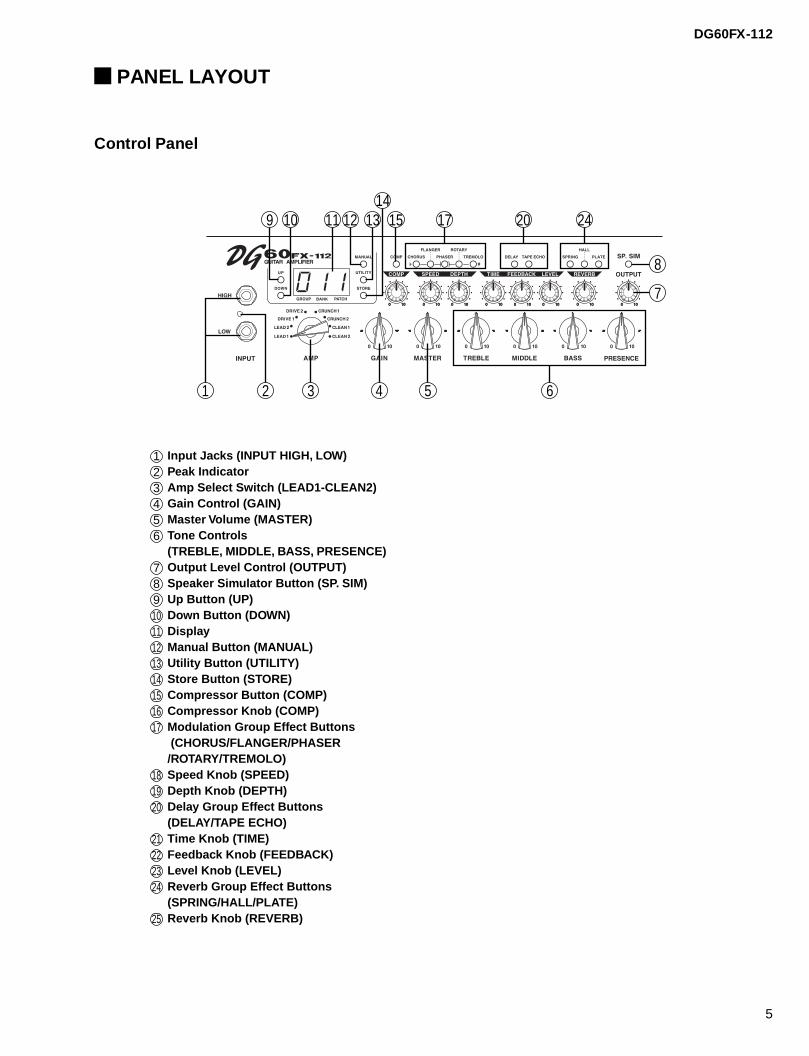
PANEL LAYOUT
Input Jacks (INPUT HIGH, LOW)Peak IndicatorAmp Select Switch (LEAD1-CLEAN2)Gain Control (GAIN)Master Volume (MASTER)Tone Controls(TREBLE, MIDDLE, BASS, PRESENCE)Output Level Control (OUTPUT)Speaker Simulator Button (SP. SIM)Up Button (UP)Down Button (DOWN)DisplayManual Button (MANUAL)Utility Button (UTILITY)Store Button (STORE)Compressor Button (COMP)Compressor Knob (COMP)Modulation Group Effect Buttons (CHORUS/FLANGER/PHASER/ROTARY/TREMOLO)Speed Knob (SPEED)Depth Knob (DEPTH)Delay Group Effect Buttons(DELAY/TAPE ECHO)Time Knob (TIME)Feedback Knob (FEEDBACK)Level Knob (LEVEL)Reverb Group Effect Buttons(SPRING/HALL/PLATE)Reverb Knob (REVERB)
Control Panel
1 2 43
7
5 6
8
24201711 129 15131014
DG60FX-112
6
34353637
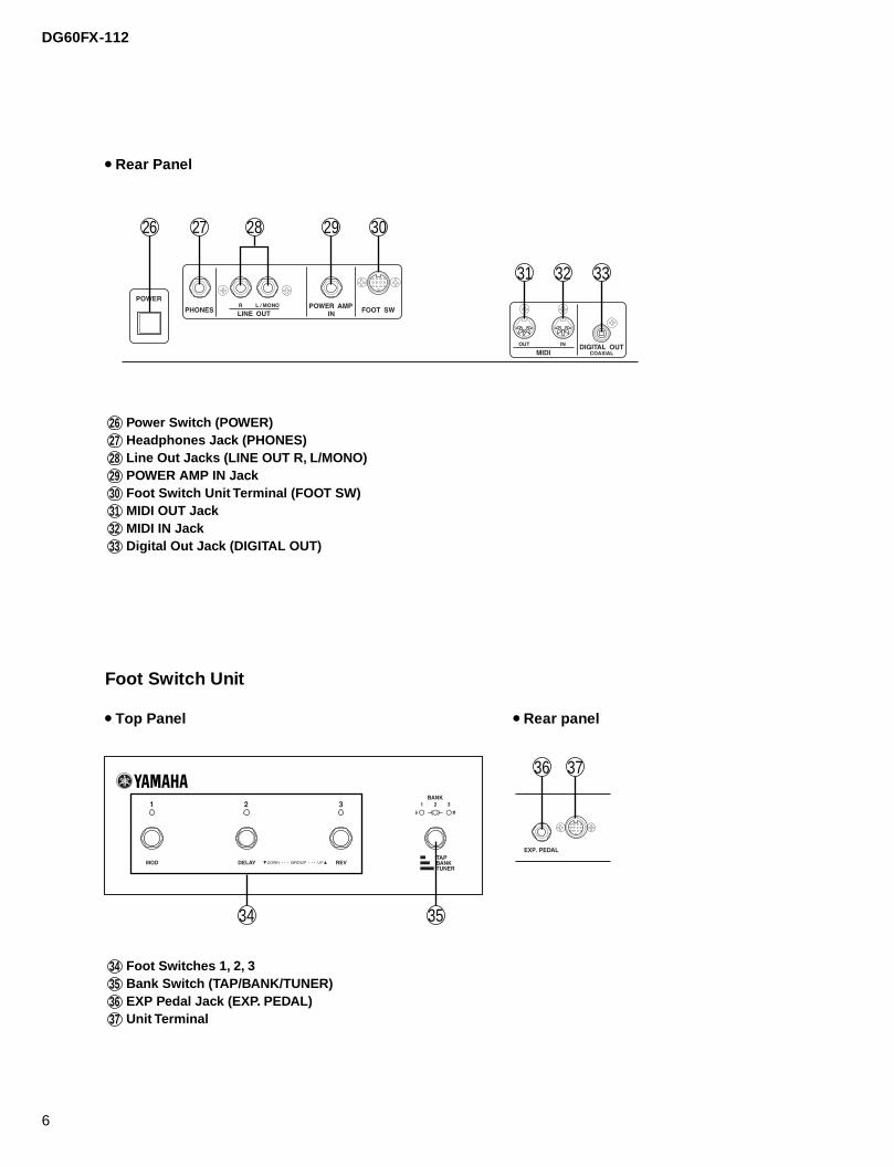
2627282930313233
Power Switch (POWER)Headphones Jack (PHONES)Line Out Jacks (LINE OUT R, L/MONO)POWER AMP IN JackFoot Switch Unit Terminal (FOOT SW)MIDI OUT JackMIDI IN JackDigital Out Jack (DIGITAL OUT)
Foot Switches 1, 2, 3Bank Switch (TAP/BANK/TUNER)EXP Pedal Jack (EXP. PEDAL)Unit Terminal
Rear Panel
Top Panel Rear panel
26 27 2928 30
31 32 33
34 35
36 37
Foot Switch Unit
DG60FX-112
7
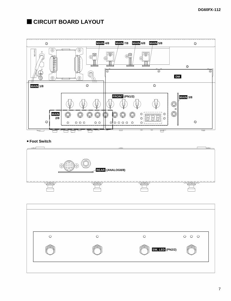
CIRCUIT BOARD LAYOUT
4/8 7/8 6/8 5/8
1/8
2/8
3/8(PN1/2)
MAIN MAIN MAIN MAIN
MAIN
DM
MAIN
MAINFRONT
(ANALOG8/8)REAR
(PN2/2)SW, LED
Foot Switch
DG60FX-112
8
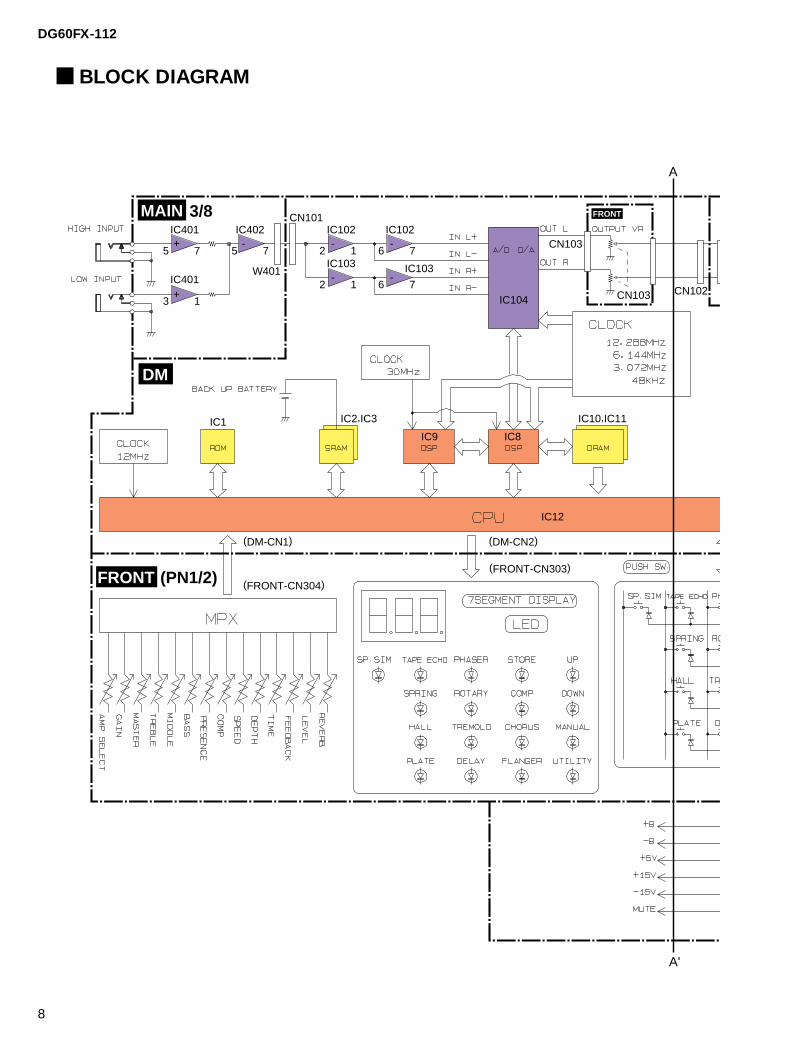
BLOCK DIAGRAM
(PN1/2)
3/8
IC1
IC12
(DM-CN1)
(FRONT-CN304)
(DM-CN2)
(FRONT-CN303)
IC2,IC3
IC9 IC8
IC10,IC11
IC401 IC402
W401
CN101
IC401
+
+
5 7 5 7
13
IC102--
2 1IC103
1-
2
IC102-
6 7
IC103
6-
7IC104
CN103
CN103 CN102
FRONT
MAIN
DM
FRONT
A
A'
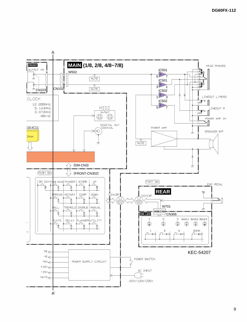
DG60FX-112
9
KEC-54207
(DM-CN3)
(FRONT-CN302)
W701
CN306
C10,IC11
CN103
W502
CN102
IC501+
75IC501+
3 1IC502+
1 3IC502+
5 7
REAR
(1/8, 2/8, 4/8~7/8)MAINFRONT
SW, LED
A
A'
DG60FX-112
10
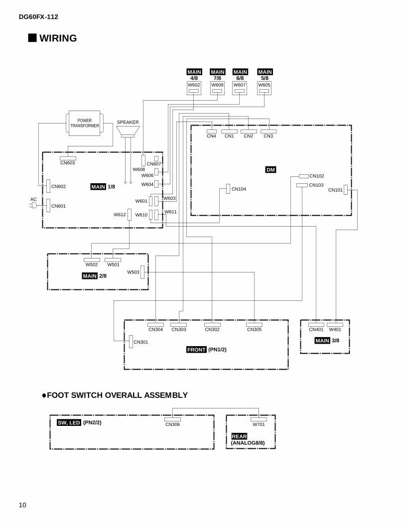
WIRING
SPEAKER
CN603
CN602
CN301
CN601
AC
TRANSFORMERPOWER
W502 W501
CN304 CN303 CN302 CN305
W701CN306
CN401 W401
CN4
W503
CN1 CN2 CN3
CN103CN104
W612
W608CN607
W606
W604
W601W603
W611W610
W6024/8 7/8
W6096/8
W6075/8
W605
1/8
2/8
3/8
(PN1/2)
CN102
CN101
MAIN MAIN MAIN MAIN
DM
MAIN
MAIN
(ANALOG8/8)REAR
MAIN
(PN2/2)SW, LED
FRONT
FOOT SWITCH OVERALL ASSEMBLY
DG60FX-112
11
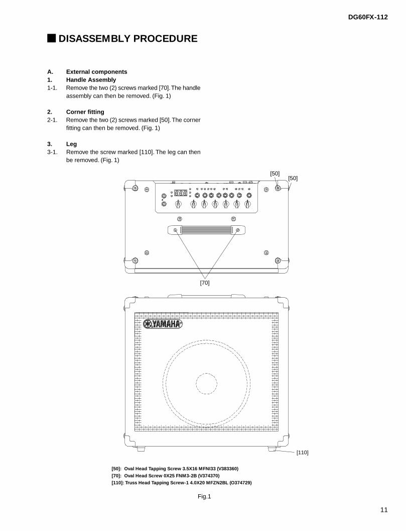
DISASSEMBLY PROCEDURE
Fig.1
A. External components1. Handle Assembly1-1. Remove the two (2) screws marked [70]. The handle
assembly can then be removed. (Fig. 1)
2. Corner fitting2-1. Remove the two (2) screws marked [50]. The corner
fitting can then be removed. (Fig. 1)
3. Leg3-1. Remove the screw marked [110]. The leg can then
be removed. (Fig. 1)
[50]: Oval Head Tapping Screw 3.5X16 MFNI33 (V383360)
[70]: Oval Head Screw 0X25 FNM3-2B (V374370)
[110]: Truss Head Tapping Screw-1 4.0X20 MFZN2BL (O374729)
[110]
[70]
[50][50]
DG60FX-112
12
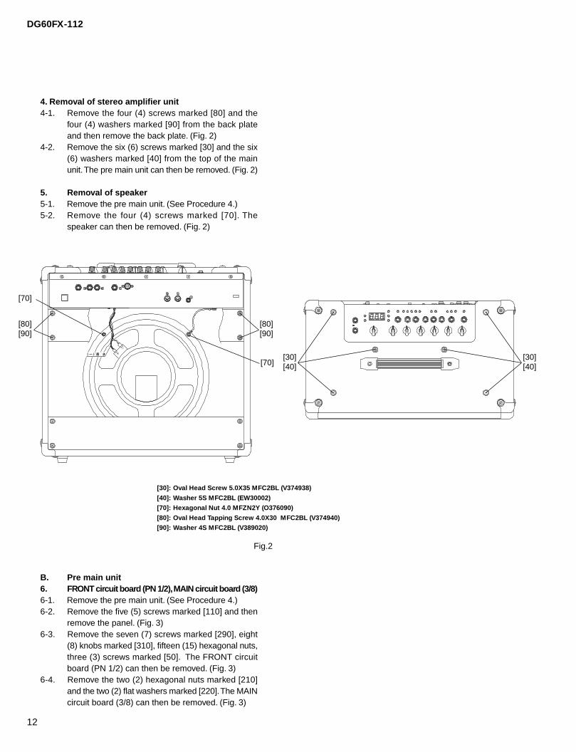
Fig.2
4. Removal of stereo amplifier unit4-1. Remove the four (4) screws marked [80] and the
four (4) washers marked [90] from the back plateand then remove the back plate. (Fig. 2)
4-2. Remove the six (6) screws marked [30] and the six(6) washers marked [40] from the top of the mainunit. The pre main unit can then be removed. (Fig. 2)
5. Removal of speaker5-1. Remove the pre main unit. (See Procedure 4.)5-2. Remove the four (4) screws marked [70]. The
speaker can then be removed. (Fig. 2)
[30]: Oval Head Screw 5.0X35 MFC2BL (V374938)
[40]: Washer 5S MFC2BL (EW30002)
[70]: Hexagonal Nut 4.0 MFZN2Y (O376090)
[80]: Oval Head Tapping Screw 4.0X30 MFC2BL (V374940)
[90]: Washer 4S MFC2BL (V389020)
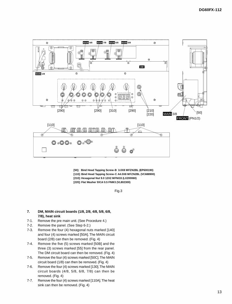
B. Pre main unit6. FRONT circuit board (PN 1/2), MAIN circuit board (3/8)6-1. Remove the pre main unit. (See Procedure 4.)6-2. Remove the five (5) screws marked [110] and then
remove the panel. (Fig. 3)6-3. Remove the seven (7) screws marked [290], eight
(8) knobs marked [310], fifteen (15) hexagonal nuts,three (3) screws marked [50]. The FRONT circuitboard (PN 1/2) can then be removed. (Fig. 3)
6-4. Remove the two (2) hexagonal nuts marked [210]and the two (2) flat washers marked [220]. The MAINcircuit board (3/8) can then be removed. (Fig. 3)
[30][40]
[30][40]
[70]
[80][90] [90]
[80]
[70]
DG60FX-112
13
7. DM, MAIN circuit boards (1/8, 2/8, 4/8, 5/8, 6/8,7/8), heat sink
7-1. Remove the pre main unit. (See Procedure 4.)7-2. Remove the panel. (See Step 6-2.)7-3. Remove the four (4) hexagonal nuts marked [140]
and four (4) screws marked [50A]. The MAIN circuitboard (2/8) can then be removed. (Fig. 4)
7-4. Remove the five (5) screws marked [50B] and thethree (3) screws marked [55] from the rear panel.The DM circuit board can then be removed. (Fig. 4)
7-5. Remove the four (4) screws marked [50C]. The MAINcircuit board (1/8) can then be removed. (Fig. 4)
7-6. Remove the four (4) screws marked [130]. The MAINcircuit boards (4/8, 5/8, 6/8, 7/8) can then beremoved. (Fig. 4)
7-7. Remove the four (4) screws marked [110A]. The heatsink can then be removed. (Fig. 4)
Fig.3
[50]: Bind Head Tapping Screw-B 3.0X8 MFZN2BL (EP600190)
[110]: Bind Head Tapping Screw-C A4.0X8 MFZN2BL (VC688900)
[210]: Hexagonal Nut 9.0 12X2 MFNI33 (LX200060)
[220]: Flat Washer 9X14 0.5 FNM3 (VL802300)
[110]
4/8 7/8 6/8 5/8
1/8
[110]
[210][220]
[290][310][290][290]MAIN 3/8
FRONT (PN1/2)
[50]
MAIN MAIN MAIN MAIN
MAIN
DM
DG60FX-112
14
Battery VN103500VN103600(Battery holder for VN103500)
• Notice for back-up battery removal Push the battery as shows in figure, then the battery will pop up.
Fig.4
[50]: Bind Head Tapping Screw-B 3.0X8 MFZN2BL (EP600190)
[55]: Bind Head Tapping Screw-P 3.0X12 MFZN2BL (VC161100)
[110]: Bind Head Tapping Screw-C A4.0X8 MFZN2BL (VC688900)
[130]: Bind Head Screw SP 3.0X12 MFZN2Y (VB763800)
[140]: Hexagonal Nut 12.0 14X2 MFC2BL (VD794100)
8. Power transformer8-1. Remove the pre main unit. (See Procedure 4.)8-2. Remove the panel. (See Step 6-2.)8-3. Remove the four (4) screws marked [110B]. The
transformer can then be removed. (Fig. 4)
[140] [140]
[50A] [50A] [55]
[50B]
[50B]
[50C]
[50C]
[50C]
[110B] [110A] [50B][130] [110A] [130] [110A] [130] [110A] [130]
DM
MAIN 1/8
MAIN 2/8
PowerTransformer
Rear panel
DG60FX-112
15
C. Foot switch9. Foot switch9-1. Remove the six (6) screws marked [110A] and then
remove the bottom plate. (Fig. 5)9-2. Remove the two (2) screws marked [110B] and
hexagonal nuts marked [90] and then remove theREAR circuit board (MAIN 8/8). (Fig. 5)
9-3. Remove the four (4) hexagonal nuts from the footswitch. The SW, LED circuit board (PN2/2) can thenbe removed. (Fig. 5)
Fig.5
[90]: Hexagonal Nut 9.0 12X2 MFNI33 (LX200060)
[110]: Bind Head Tapping Screw-B 3.0X8 MFZN2BL (EP600190)
[110A]
[110A]
[110A]
[110A]
[90]
[110B]
Hexagonal nut Hexagonal nut
Foot switch
REAR (MAIN 8/8)
SW, LED (PN2/2)
View A
DG60FX-112
16
LSI PIN DESCRIPTION
PINNO.
123456789
1011121314151617181920212223242526272829303132333435363738394041424344454647484950
I/O
OO
IIIIIIIIO
OOIIOI
I/OI/OI/OI/O
I/OI/OI/OI/OI/OI/OI/OI/OI/OI/OI/OI/O
OOOOOOOO
OOOO
PA6PA7VCCPB0PB1PB2PB3PB4PB5
PB6//DREQ0PB7//DREQ1/RESOVSS
P90/TXD0P91/TXD1P92/RXD0P93/RXD1P94/SCK0P95/SCK1P40/D0P41/D1P42/D2P43/D3
VSSP44/D4P45/D5P46/D6P47/D7
D8D9D10D11D12D13D14D15VCCA0A1A2A3A4A5A6A7
VSSA8A9A10A11
NAME
Port AAddress busPower supply
Port B
ResetGroundTransmit data (MIDI OUT)KSN-ACKReceive data (MIDI IN)KSN-RXPort 9Port 9
(Ground)
Data bus
Power supply
Address bus
(Ground)
FUNCTION PINNO.
51525354555657585960616263646566676869707172737475767778798081828384858687888990919293949596979899
100
I/O
OOOOOOOO
IIIOIII
IO
OOOOIII
IIIIIIIII
OOOOO
IIIOOO
A12A13A14A15A16A17A18A19VSS
P60//WAITP61//BREQP62//BACK
Ø/STBY/RESNMIVSS
EXTALXTALVCC/AS/RD
/HWR/LWRMD0MD1MD2
AVCCVREF
P70/AN0P71/AN1P72/AN2P73/AN3P74/AN4P75/AN5P76/AN6P77/AN7
AVSSP80
P81//CS3P82//CS2P83//CS1P84//CS0
VSSPA0PA1PA2PA3PA4PA5
NAME
Address bus
Ground
Port 6
ØoutStand-by mode signalResetNon-maskable interruptGroundClockClockPower supplyAddress strobeRead strobeWrite strobe (High)Write strobe (Low)
Mode select
Analog power supplyReference voltageAnalog data input (EQ)Analog input (EQ)Analog data input Analog input (CS)Analog data input (BEND)Analog input (MOD)Analog input (FC)Analog input (BAT)Analog groundPort 8
Chip select
Ground
Port A
FUNCTION
HD6413002FP16 (XQ375A00) CPU <H8/3002> DM: IC12
PINNO.
I/O FUNCTIONNAME PINNO.
I/O FUNCTIONNAME
1234
567
8
VssMCLKDM0DM1
RESWCINDIN
VDD
III
III
GroundMaster clock inputDIN/BCLK/WCLK format selectDM1,DM0=0,0 DSP,LDSP (64 bit,LSB first)DM1,DM0=0,1stereo,DSP (64 bit,MSB first)DM1,DM0=1,0 DSP2 (128 bit,MSB first)DM1,DM0=1,1 BB (64 bit,MSB first)System resetWord clock inputDigital audio serial data input
Power supply (+5 V)
9101112
131415
16
MUTEVFLCCKCIN
CLDCNTRCSM
DOUT
IIII
III
O
MuteValidity flagC,U bit clock input/C bit data inputC,U bit data input/U bit data input
End of C,U bit input/16,20 bit/24 bit select32 bit counter reset/Top of blockChannel status input mode select CSM=0 Asynchronous mode CSM=1 Synchronous modeDigital interface formatted data output
YM3437C-F (XM530A00) DIT2 (Digital Format Interface Transmitter) DM: IC17
DG60FX-112
17
PINNO.
I/O FUNCTIONNAME PINNO.
I/O FUNCTIONNAME
123456789
10111213141516171819202122232425262728293031323334353637383940414243444546474849505152535455565758596061626364656667686970717273747576777879808182838485868788
VddVssXIXOVdd
/SYNCI/SYNCO
VddCKICKO
CKSELVss
MCKS/SSYNC
/IC/TESTBTYP/IRQTRIGVddVss/CS/WR/RDCA7CA6CA5CA4CA3CA2CA1VssVdd
CD15CD14CD13CD12CD11CD10CD09CD08CD07CD06VssVddVdd
CD05CD04CD03CD02CD01CD00/WAITVssSI0SI1SI2SI3SI4SI5SI6SI7VssVddSO0SO1SO2SO3SO4SO5SO6SO7Vss
DB00DB01DB02DB03DB04DB05DB06DB07DB08DB09DB10DB11DB12VddVdd
IO
IO
IOI
IIIIIOI/O
III
I/OI/OI/OI/OI/OI/OI/O
I/OI/OI/OI/OI/OI/OI/OI/OI/OI/O
I/OI/OI/OI/OI/OI/OO
IIIIIIII
OOOOOOOO
I/OI/OI/OI/OI/OI/OI/OI/OI/OI/OI/OI/OI/O
Power supply (3.3 V)GroundSystem master clock input (60 MHz or 30 MHz)System master clock output (High or 30 MHz)Power supply (5 V)Sync. signal inputSync. signal outputPower supply (5 V)System clock input (30 MHz)System clock output (30 MHz)System master clock select (0: 60 MHz, 1: 30 MHz)GroundSerial I/O master clock input (128 x Fs)Serial I/O Sync. signal outputInitial clearTest mode setting (0: Test, 1: Normal)Data bus type select (0: 8 bit, 1: 16 bit)IRQ outputTrigger signal input/outputPower supply (5 V)Groundchip select signal inputWrite signal inputRead signal input
Address bus of internal register
GroundPower supply (3.3 V)
Data bus of internal register
GroundPower supply (3.3 V)Power supply (5 V)
Data bus of internal register
WAIT outputGround
Serial data input
GroundPower supply (5 V)
Serial data output
Ground
Parallel data bus
Power supply (5 V)Power supply (3.3 V)
8990919293949596979899
100101102103104105106107108109110111112113114115116117118119120121122123124125126127128129130131132133134135136137138139140141142143144145146147148149150151152153154155156157158159160161162163164165166167168169170171172173174175176
VssDB13DB14DB15DB16DB17DB18DB19DB20DB21DB22VssVdd
DB23DB24DB25DB26DB27DB28DB29DB30DB31
TIMO/DBOBVssVdd
DA00DA01DA02DA03DA04DA05DA06DA07Vss
DA08DA09DA10DA11DA12DA13DA14DA15VssVdd(n.c)Vdd
DA16DA17DA18DA19DA20DA21DA22DA23Vss
DA24DA25DA26DA27DA28DA29DA30DA31VddVssA00A01A02A03A04A05A06A07A08A09VssVddA10A11A12A13A14
A15/RASA16/CASA17/CE
/WE/OEVdd
I/OI/OI/OI/OI/OI/OI/OI/OI/OI/O
I/OI/OI/OI/OI/OI/OI/OI/OI/OI/O
I/OI/OI/OI/OI/OI/OI/OI/O
I/OI/OI/OI/OI/OI/OI/OI/O
I/OI/OI/OI/OI/OI/OI/OI/O
I/OI/OI/OI/OI/OI/OI/OI/O
OOOOOOOOOO
OOOOOOOOOO
Ground
Parallel data bus
GroundPower supply (3.3 V)
Parallel data bus
Timing signal output/ Parallel data bus output/ inputGroundPower supply (5 V)
Memory data bus
Ground
Memory data bus
GroundPower supply (3.3 V)Not usedPower supply (5 V)
Memory data bus
Ground
Memory data bus
Power supply (5 V)Ground
Memory address (SRAM, PSRAM, DRAM)
GroundPower supply (3.3 V)
Memory address (SRAM, PSRAM, DRAM)
Memory address (SRAM, PSRAM)
Memory address (SRAM, PSRAM), /RAS (DRAM)Memory address (SRAM, PSRAM), /CAS (DRAM)Memory address (SRAM), /CE (PSRAM)Memory write enable signalMemory output enable signalPower supply (5 V)
YSS910-S (XV988A00) DSP6 (Digital Signal Processor) DM: IC8, IC9
DG60FX-112
18
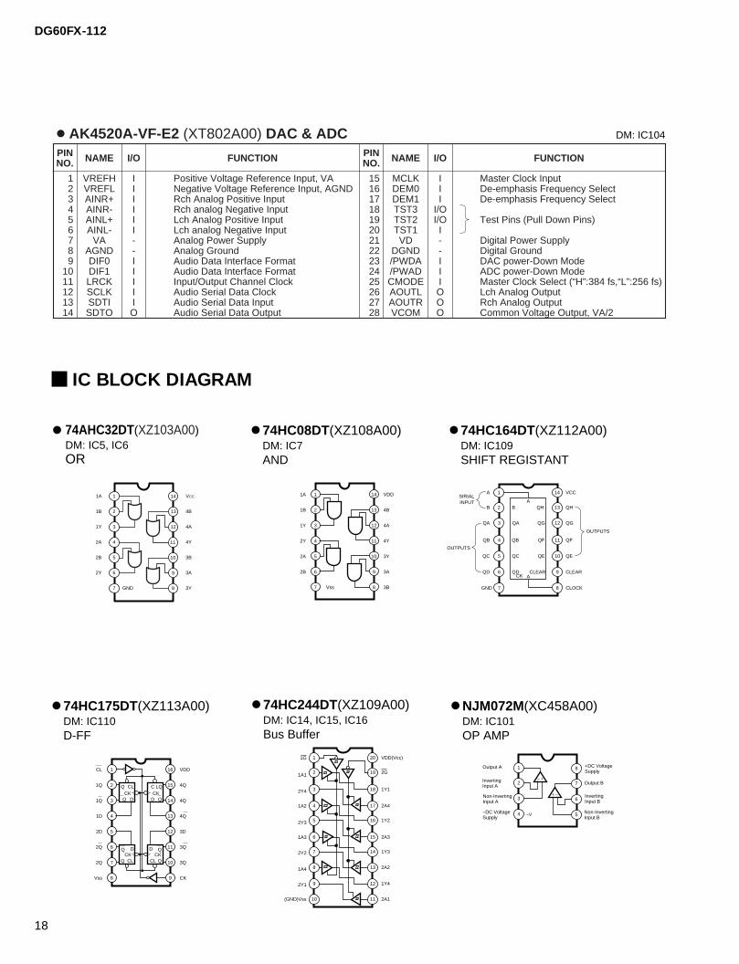
IC BLOCK DIAGRAM
PINNO.
123456789
1011121314
I/O
IIIIII--IIIIIO
VREFHVREFLAINR+AINR-AINL+AINL-
VAAGNDDIF0DIF1LRCKSCLKSDTISDTO
NAME
Positive Voltage Reference Input, VANegative Voltage Reference Input, AGNDRch Analog Positive InputRch analog Negative InputLch Analog Positive InputLch analog Negative InputAnalog Power SupplyAnalog GroundAudio Data Interface FormatAudio Data Interface FormatInput/Output Channel ClockAudio Serial Data ClockAudio Serial Data InputAudio Serial Data Output
FUNCTION PINNO.
1516171819202122232425262728
I/O
III
I/OI/OI--IIIOOO
MCLKDEM0DEM1TST3TST2TST1VD
DGND/PWDA/PWADCMODEAOUTLAOUTRVCOM
NAME
Master Clock InputDe-emphasis Frequency SelectDe-emphasis Frequency Select
Test Pins (Pull Down Pins)
Digital Power SupplyDigital GroundDAC power-Down ModeADC power-Down ModeMaster Clock Select (“H”:384 fs,“L”:256 fs)Lch Analog OutputRch Analog OutputCommon Voltage Output, VA/2
FUNCTION
AK4520A-VF-E2 (XT802A00) DAC & ADC DM: IC104
11A
2
3
4
5
6
7
1B
1Y
2A
2B
2Y
GND 8
9
10
11
12
13
14 VCC
4B
4A
4Y
3B
3A
3Y
74AHC32DT(XZ103A00) DM: IC5, IC6OR
74HC08DT(XZ108A00)DM: IC7AND
74HC244DT(XZ109A00)DM: IC14, IC15, IC16Bus Buffer
74HC164DT(XZ112A00)DM: IC109SHIFT REGISTANT
NJM072M(XC458A00)DM: IC101OP AMP
1
2
3
4
5
6
7
13
12
11
10
9
8
141A
1B
1Y
2Y
2A
2B
Vss
VDD
4B
4A
4Y
3Y
3A
3B
74HC175DT(XZ113A00)DM: IC110D-FF
Output A
InvertingInput A
Non-InvertingInput A
–DC Voltage Supply
+DC Voltage Supply
Output B
InvertingInput B
Non-InvertingInput B
1
2
3
4
8
7
6
5
– +
–+
–V
1G
1A1
2Y4
1A2
2Y3
1A3
2Y2
1A4
2Y1
1 20
2 19
3 18
4 17
5 16
6 15
7 14
8 13
9 12
10 11
VDD(Vcc)
2G
1Y1
2A4
1Y2
2A3
1Y3
2A2
1Y4
2A1 (GND)Vss
1
2
3
4
5
6
7
15
14
13
12
11
10
16CL
1Q
1Q
1D
2D
2Q
2Q
VDD
4Q
4Q
4Q
3D
3Q
3Q
8 9Vss CK
Q
Q DCK
CL
D QCK
C LQ
QCK CKCL QCL
QDQ D
1
2
3
A
QA QA
4QB QB
5QC QC
6QD QD
7GND
B B
14
13
12
VCC
QGQG
11 QFQF
10 QEQE
9 CLEARCLEAR
8 CLOCK
QH
CK
QH
OUTPUTS
OUTPUTS
SIRIALINPUT A
A
DG60FX-112
19
TC74HC4040F(XR684A00) DM: IC108B. COUNTERTC74HC4040DT(XZ111A00) DM: IC10812-Stage Binary Ripple Counter
74HC374DT(XZ102A00)DM: IC301~IC307D-FF
74HC4052DT(XZ101A00)DM: IC308, IC309Multiplexer
CK
1
2
3
4
5
6
7
Q12 Q12
Q6 Q6
Q5 Q5
Q7 Q7
Q4 Q4
Q3 Q3
Q2 Q2
16
15
14
13
12
11
10
VDD
Q11Q11
Q10Q10
Q8Q8
Q9Q9
CLRCL
8Vss 9 Q1Q1
Input Pulses ( )
Q
D
Q
D
Q
D
Q
D CK
OE OE
OE
OE OE
OEOE
OE
Q
D
Q
D
Q
D
Q
DCK
CK
CK
CK CK
CK
CK
1OUT PUTCONTROL
2
3
4
5
6
7
8
9
10
1Q
1D
2D
2Q
3Q
3D
4D
4Q
GND 11
12
13
14
15
16
17
18
19
20 VCC
8Q
8D
7D
7Q
6Q
6D
5D
5Q
CLOCK
1
2
3
4
5
6
7
OY
2Y
Y-COM
3Y
1Y
INH
VEE
16
15
14
13
12
11
10
VDD
2X
1X
X-COM
OX
3X
A
2Y
Y-COM
3Y
1Y
INH
2X
0YB
1X
X-COM
0X
3X
A
8VSS 9 B
74HCU04DT (XZ110A00)DM: IC107INVERTER
11A
2
3
4
5
6
7
1Y
2A
2Y
3A
3Y
VSS 8
9
10
11
12
13
14 VDD
6A
6Y
5A
5Y
4A
4Y
NJM5532M (XC011A00)DM: IC102, IC103, IC106OP AMP
NE5532P (IG102500)DM: IC502OP AMP
NJM4556AMT1 (XQ138A00)DM: IC105OP AMP
1
2
3
4
8
7
6
5
A OUT
A+IN
V+
B OUT
B+IN
A IN
V
B IN
NJM4556AD (XQ824A00)MAIN: IC501OP AMP
1
2
3
4 -V
+V 8
7
6
5
Output A
Non-InvertingInput A
-DC Voltage Supply
+DC VoltageSupply
Output B
InvertingInput B
Non-InvertingInput B
InvertingInput A +-
+ -
1
2
3
4 -V
8
7
6
5
Output A +V
Non-InvertingInput A
-DC Voltage Supply
+DC VoltageSupply
Output B
InvertingInput B
Non-InvertingInput B
InvertingInput A +-
+ -
MB3790PF(XR967A00)DM: IC4 ASSP
N.C.
V BAT1
V OUT
V OUT
V BAT2
ALARM1
GND
CONTROL
N.C.
V IN
V IN
V SENSE
C T
RESET
RESET
ALARM1
1
2
3
4
5
6
7
8
10
9
13
12
11
16
15
14
2
3
4
5
6
7
8
9
10
11
12
16
14
13
C T
V B
AT
2
V B
AT
1
ALARM2
RESET
RESET
ALARM1
V OUT
V OUT
V IN
V IN
V SENSE
CONTROL
GND
590kΩ
240kΩ
1.24V
Reference Voltage
Power Supply Circuit
S Q
R
R CN 0.5Ω
100Ω
SBD
2.65V
2.37V
500Ω
V IN
V IN
V OUT
V OUT
3µA
V th:3V
V th:1.5V
DG60FX-112
20
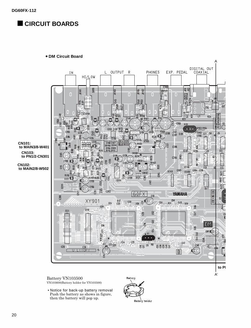
CIRCUIT BOARDS
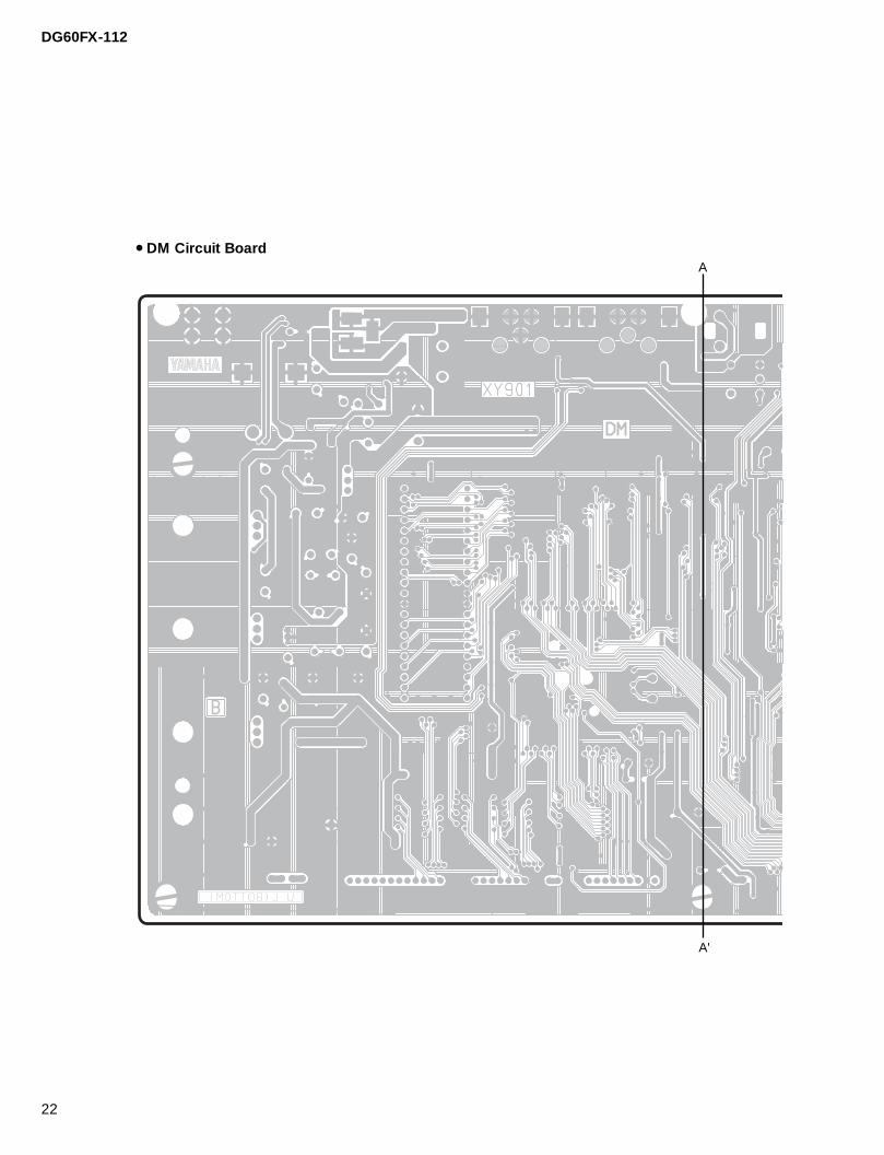
DM Circuit Board
to PN
A
A'
CN101: to MAIN3/8-W401
CN103: to PN1/2-CN301
CN102: to MAIN2/8-W502
Battery VN103500VN103600(Battery holder for VN103500)
• Notice for back-up battery removal Push the battery as shows in figure, then the battery will pop up.
21
DG60FX-112
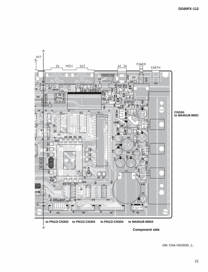
to MAIN1/8-W603
CN104: to MAIN1/8-W601
to PN1/2-CN304to PN1/2-CN303to PN1/2-CN302
A
A'Component side
DM: CNA-V620530 0
DG60FX-112
22
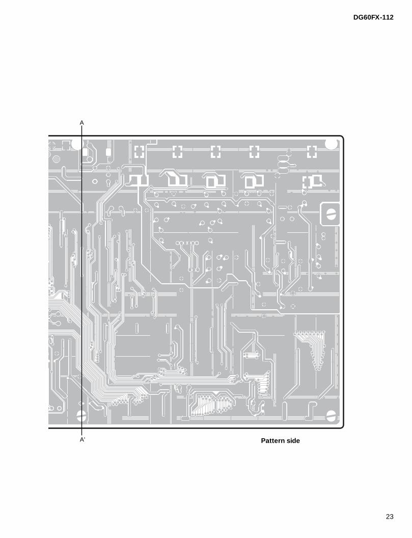
A
A'
DM Circuit Board
23
DG60FX-112
A
A' Pattern side
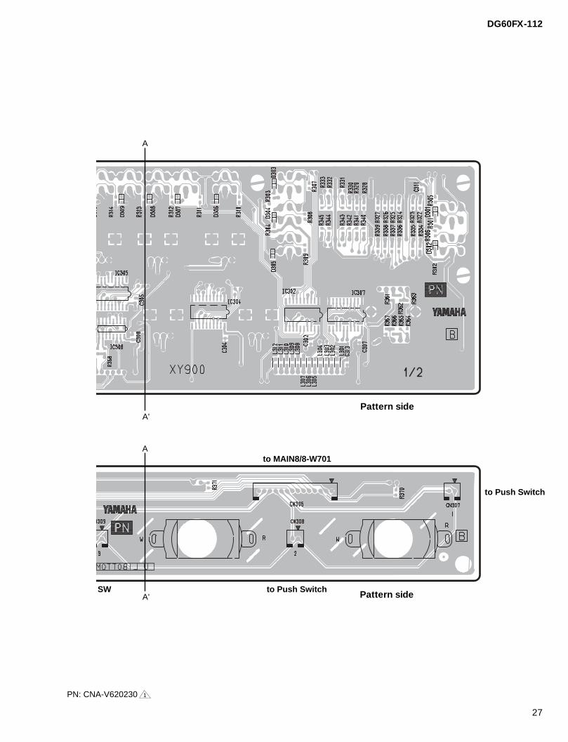
DG60FX-112
24
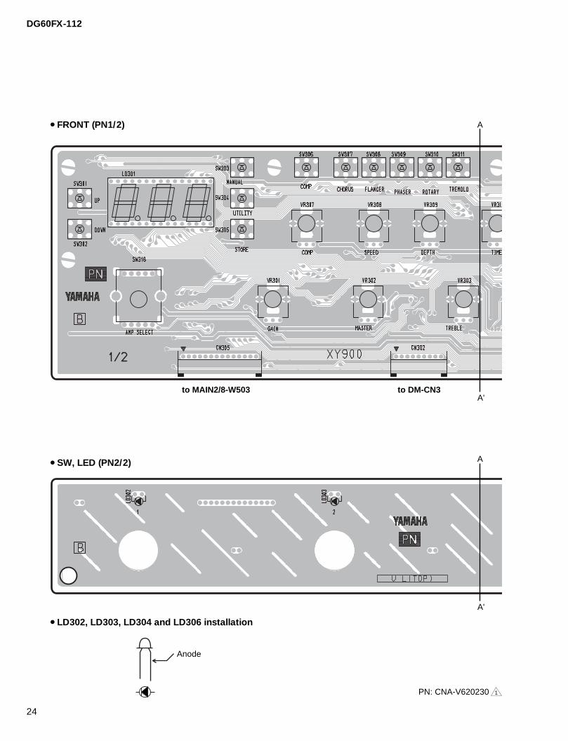
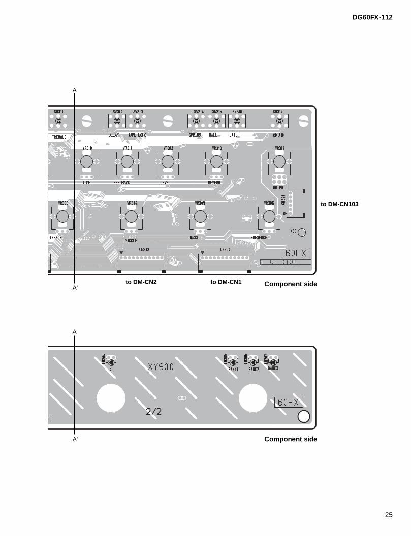
to MAIN2/8-W503 to DM-CN3
A
A'
A
A'
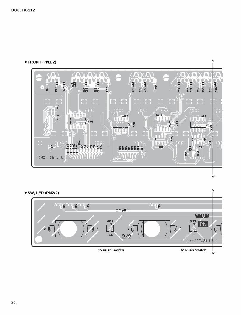
FRONT (PN1/2)
SW, LED (PN2/2)
PN: CNA-V620230 1
LD302, LD303, LD304 and LD306 installation
Anode
25
DG60FX-112
to DM-CN2 to DM-CN1
to DM-CN103
A
A'
A
A'
Component side
Component side
DG60FX-112
26
to Push Switchto Push Switch
A
A'
A
A'
FRONT (PN1/2)
SW, LED (PN2/2)
27
DG60FX-112
to MAIN8/8-W701
to Push Switch
to Push Switch
SW
A
A'
A
A'
Pattern side
Pattern side
PN: CNA-V620230 1
DG60FX-112
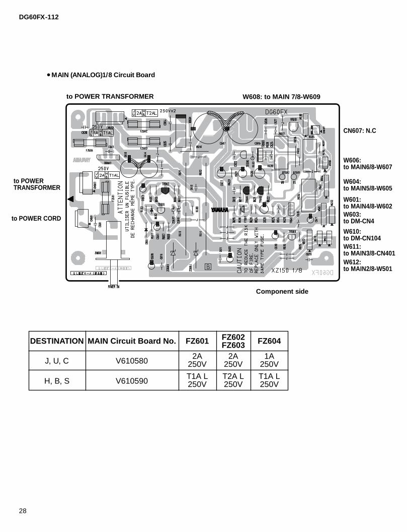
28
to POWER TRANSFORMER
to POWER TRANSFORMER W608: to MAIN 7/8-W609
CN607: N.C
W606:to MAIN6/8-W607
W604:to MAIN5/8-W605
W601: to MAIN4/8-W602W603: to DM-CN4
W610: to DM-CN104W611: to MAIN3/8-CN401W612: to MAIN2/8-W501
to POWER CORD
MAIN (ANALOG)1/8 Circuit Board
Component side
MAIN Circuit Board No.
V610580
V610590
J, U, C
H, B, S
2A250V
T1A L250V
2A250V
T2A L250V
1A250V
T1A L250V
FZ601 FZ602FZ603 FZ604DESTINATION
29
DG60FX-112
to MIAN1/8-W601 to MIAN1/8-W604
to MIAN1/8-W606 to MIAN1/8-W608to DM-CN101
to DM-CN102
to MAIN1/8-W611
to MAIN1/8-W612
to PN1/2-CN305
to PN2/2-CN306
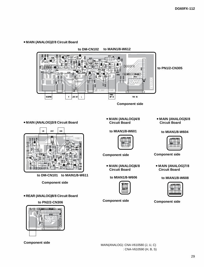
MAIN (ANALOG)2/8 Circuit Board
Component side
MAIN (ANALOG)3/8 Circuit Board
Component side
REAR (ANALOG)8/8 Circuit Board
Component side
Component side
MAIN (ANALOG)6/8 Circuit Board
Component side
Component side
MAIN (ANALOG)7/8 Circuit Board
Component side
MAIN (ANALOG)4/8 Circuit Board
MAIN (ANALOG)5/8 Circuit Board
MAIN(ANALOG): CNA-V610580 (J, U, C): CNA-V610590 (H, B, S)
DG60FX-112
30
TEST PROGRAM
A. PREPARATION• EXP. PEDAL Connect the B50KVR.• DIGITAL OUT Connect the DA converter.• MIDI IN Connect IN and OUT, using the DIN• MIDI IN 5P cable.• The input signal is a 1kHz sine wave.• Set all rotary VR’s and switches near their center
position.• Set the OUTPUT VR to the MAX position.• Set the input impedance of the measuring instrument
to 1Mohm or more.
B. CONTENTS OF TEST PROGRAM0: LED Check1: SW Check2: VR Check3: Battery Check4: MIDI Check5: SRAM Check6: DSP Check
C. STARTING THE TEST PROGRAMWhile pressing the MANUAL, STORE and HALLswitches, turn on the POWER switch. The TESTprogram will then be started.
D. SELECTING THE TEST NUMBERUsing the UP and DOWN switches, select the testnumber and press the STORE switch to confirmselection.
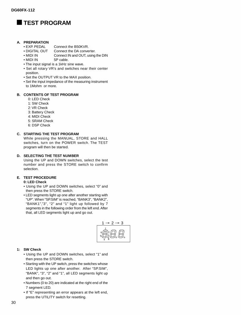
E. TEST PROCEDURE0: LED Check• Using the UP and DOWN switches, select “0” and
then press the STORE switch.• LED segments light up one after another starting with
“UP”. When “SP.SIM” is reached, “BANK3”, “BANK2”,“BANK1”,”3", “2” and “1” light up followed by 7segments in the following order from the left end. Afterthat, all LED segments light up and go out.
1
1 2 3
7
84
23
6
5
1: SW Check• Using the UP and DOWN switches, select “1” and
then press the STORE switch.• Starting with the UP switch, press the switches whose
LED lights up one after another. After “SP.SIM”,“BANK”, “3”, “2” and “1”, all LED segments light upand then go out.
• Numbers (0 to 20) are indicated at the right end of the7 segment LED.
• If “E” representing an error appears at the left end,press the UTILITY switch for resetting.
31
DG60FX-112
2: VR Check• Using the UP and DOWN switches, select “2” and
then press the STORE switch.• Press switches in the order of “AMP SELECT”, “GAIN”
until “PRESENCE, then from “COMP” to “REVERB”and finally until “EXP.PEDAL” is reached.
• Turn the control fully in the direction toward the left 7segment LED which is turned on. If the test result isOK, the right 7 segment LED lights up. Then turn thecontrol to that direction. If the test result is OK, proceedto the next VR. After completing this check, return thecontrol to the center position.
• If an error exists outside of the control being checked,“E” meaning an error appears at the left end OF LED.In such case, press the UTILITY switch for resetting.
• At the end of all VR checks, all LED segments light upand go out. Then checking advances to the next step.
3: Battery Check• Using the UP and DOWN switches, select “3” and
then press the STORE switch.• If the check result is OK, all LED segments light up
and go out. Then checking advances to the next step.• In case of an error, “E” is indicated by LED.
4: MIDI Check• Using the UP and DOWN switches, select “4” and
then press the STORE switch.• If the check result is OK, all LED segments light up
and go out. Then checking advances to the next step.• In case of an error, “E” is indicated by LED.• The numeric figure at the right end of LEF represents,
0: transmission and 1: reception.
5: SRAM Check• Using the UP and DOWN switches, select “5” and
then press the STORE switch.• If the check result is OK, all LED segments light up
and go out. Then checking advances to the next step.• The numeric figure at the right end of LEF represents,
0: IC2 and 1: IC3.
DG60FX-112
32
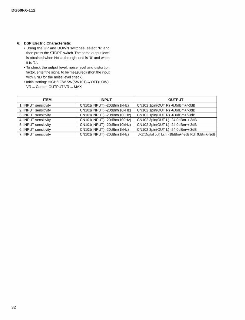
1. INPUT sensitivity2. INPUT sensitivity3. INPUT sensitivity4. INPUT sensitivity5. INPUT sensitivity6. INPUT sensitivity7. INPUT sensitivity
ITEM INPUT OUTPUT
CN101(INPUT) -20dBm(1kHz)CN101(INPUT) -20dBm(10kHz)CN101(INPUT) -20dBm(100Hz)CN101(INPUT) -20dBm(100Hz)CN101(INPUT) -20dBm(10kHz)CN101(INPUT) -20dBm(1kHz)CN101(INPUT) -20dBm(1kHz)
CN102 1pin(OUT R) -6.0dBm+/-3dBCN102 1pin(OUT R) -6.0dBm+/-3dBCN102 1pin(OUT R) -6.0dBm+/-3dBCN102 3pin(OUT L) -24.0dBm+/-3dBCN102 3pin(OUT L) -24.0dBm+/-3dBCN102 3pin(OUT L) -24.0dBm+/-3dB JK2(Digital out) Lch -18dBm+/-3dB Rch 0dBm+/-3dB
6: DSP Electric Characteristic• Using the UP and DOWN switches, select “6” and
then press the STORE switch. The same output levelis obtained when No. at the right end is “0” and whenit is “1”.
• To check the output level, noise level and distortionfactor, enter the signal to be measured (short the inputwith GND for the noise level check).
• Initial setting: HIGH/LOW SW(SW101) ••• OFF(LOW),VR ••• Center, OUTPUT VR ••• MAX
33
DG60FX-112
ERROR MESSAGES
IDLING ADJUSTMENT
If an error occurs during operation, one of the following error message numbers will appear on the display.
E1:MIDI Receive Buffer FullCAUSE: Too much MIDI data is being received by the DG amplifier at one time.SOLUTION: Try reducing the amount of data being sent or, break the data into smaller blocks.
E2:Communication Error.CAUSE: An abnormality is detected during MIDI communications.SOLUTION: Check all connections, etc. and try again.
E3:Bulk Receive Check Sum Error.CAUSE: The check sum does not match the received MIDI bulk data.SOLUTION: Check all connections and data, and try again.
E4:Bulk Receive Data Abnormality.CAUSE: An abnormality is detected in the received MIDI bulk data.SOLUTION: Check all connections and data, and try again.
E5:Backup Battery Error.CAUSE: Backup battery power is depleted.SOLUTION: Continued use of the device will result in the loss of data. Return the device to the music dealer where
you purchased it or, the nearest Yamaha Service center and have the battery replaced.
1. Turn the id l ing adjustment volume (VR601)counterclockwise fully.
2. Adjust the VR601 so that the DC voltage between theterminals of the CN607 is 3mV.
DG60FX-112
34
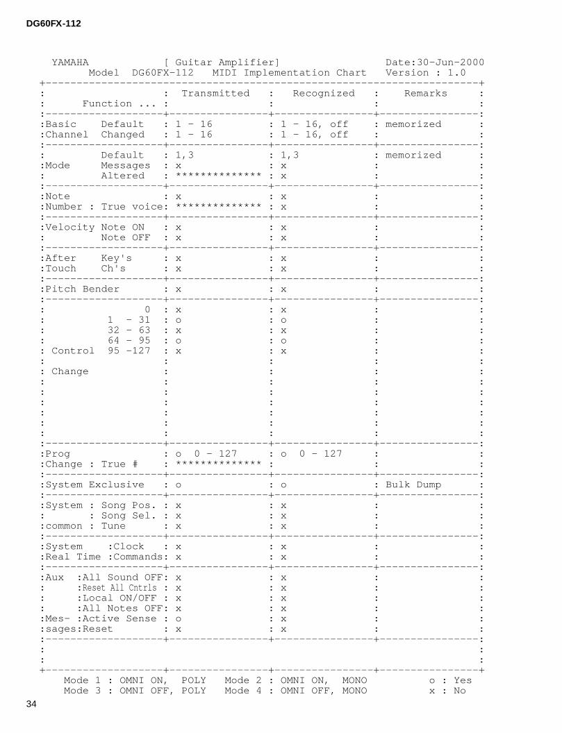
YAMAHA [ Guitar Amplifier] Date:30-Jun-2000 Model DG60FX-112 MIDI Implementation Chart Version : 1.0+----------------------------------------------------------------------+: : Transmitted : Recognized : Remarks :: Function ... : : : ::-------------------+----------------+----------------+----------------::Basic Default : 1 - 16 : 1 - 16, off : memorized ::Channel Changed : 1 - 16 : 1 - 16, off : ::-------------------+----------------+----------------+----------------:: Default : 1,3 : 1,3 : memorized ::Mode Messages : x : x : :: Altered : ************** : x : ::-------------------+----------------+----------------+----------------::Note : x : x : ::Number : True voice: ************** : x : ::-------------------+----------------+----------------+----------------::Velocity Note ON : x : x : :: Note OFF : x : x : ::-------------------+----------------+----------------+----------------::After Key's : x : x : ::Touch Ch's : x : x : ::-------------------+----------------+----------------+----------------::Pitch Bender : x : x : ::-------------------+----------------+----------------+----------------:: 0 : x : x : :: 1 - 31 : o : o : :: 32 - 63 : x : x : :: 64 - 95 : o : o : :: Control 95 -127 : x : x : :: : : : :: Change : : : :: : : : :: : : : :: : : : :: : : : :: : : : :: : : : ::-------------------+----------------+----------------+----------------::Prog : o 0 - 127 : o 0 - 127 : ::Change : True # : ************** : : ::-------------------+----------------+----------------+----------------::System Exclusive : o : o : Bulk Dump ::-------------------+----------------+----------------+----------------::System : Song Pos. : x : x : :: : Song Sel. : x : x : ::common : Tune : x : x : ::-------------------+----------------+----------------+----------------::System :Clock : x : x : ::Real Time :Commands: x : x : ::-------------------+----------------+----------------+----------------::Aux :All Sound OFF: x : x : :: :Reset All Cntrls : x : x : :: :Local ON/OFF : x : x : :: :All Notes OFF: x : x : ::Mes- :Active Sense : o : x : ::sages:Reset : x : x : ::-------------------+----------------+----------------+----------------:: :: :+-------------------+----------------+----------------+----------------+ Mode 1 : OMNI ON, POLY Mode 2 : OMNI ON, MONO o : Yes Mode 3 : OMNI OFF, POLY Mode 4 : OMNI OFF, MONO x : No
WARNINGComponents having special characteristics are marked and must be replaced with parts havingspecification equal to those originally installed.
Notes : DESTINATION ABBREVIATIONS
The numbers “QTY” show quantities for each unit.The parts with “--” in “PART NO.” are not available as spare parts.This mark “ ” in the REMARKS column means these parts are interchangeable.The second letter of the shaded ( ) part number is O, not zero.The second letter of the shaded ( ) part number is I, not one.
M: South African modelO : Chinese modelQ : South-east Asia modelT : Taiwan modelU : U.S.A. modelV : General export model (110V)W: General export model (220)N,X : General export modelY : Export model
A : Australian modelB : British modelC : Canadian modelD : German modelE : European modelF : French modelH : North European modelI : Indonesian modelJ : Japanese model
GUITAR AMPLIFIER
PARTS LIST CONTENTS
OVERALL ASSEMBLY .............................................. 2PRE MAIN UNIT .................................. 4FOOT SWITCH ............................................ 6ELECTRICAL PARTS ............................................. 7
DG60FX-112
2
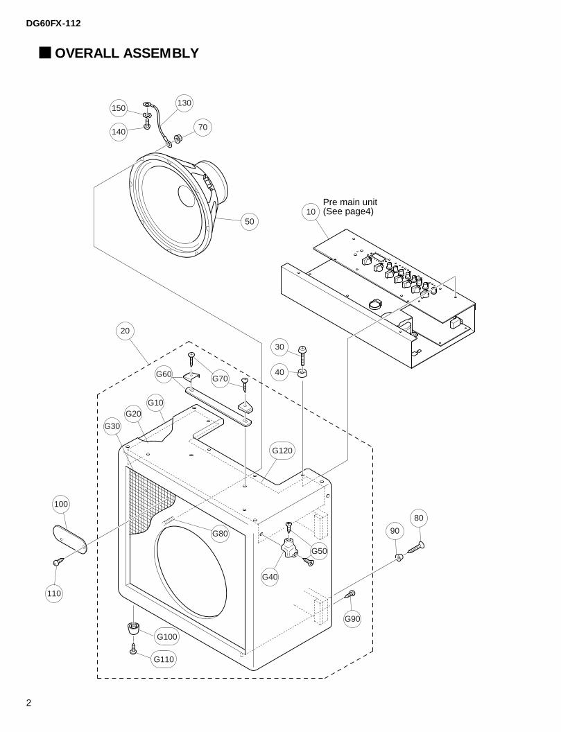
OVERALL ASSEMBLY
130
70
50
20
30
80
90
G90
G50
G40
G30
G20G10
G70G60
110
100
40
10
150
140
G80
G100
G120
G110
Pre main unit(See page4)
DG60FX-112
3
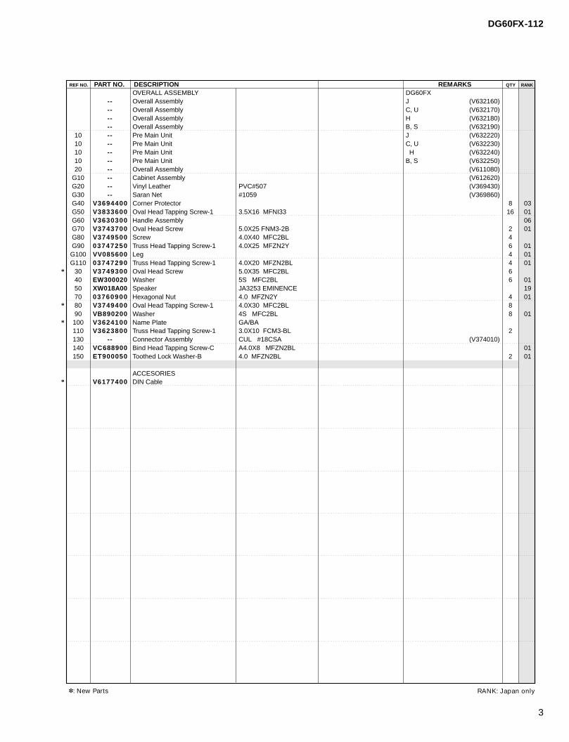
: New Parts
REF NO. PART NO. DESCRIPTION REMARKS QTY RANK
RANK: Japan only
*
*
*
*
OVERALL ASSEMBLY DG60FXOverall Assembly J (V632160)Overall Assembly C, U (V632170)Overall Assembly H (V632180)Overall Assembly B, S (V632190)
10 Pre Main Unit J (V632220)10 Pre Main Unit C, U (V632230)10 Pre Main Unit H (V632240)10 Pre Main Unit B, S (V632250)20 Overall Assembly (V611080)
G10 Cabinet Assembly (V612620)G20 Vinyl Leather PVC#507 (V369430)G30 Saran Net #1059 (V369860)G40 Corner Protector 8 03G50 Oval Head Tapping Screw-1 3.5X16 MFNI33 16 01G60 Handle Assembly 06G70 Oval Head Screw 5.0X25 FNM3-2B 2 01G80 Screw 4.0X40 MFC2BL 4G90 Truss Head Tapping Screw-1 4.0X25 MFZN2Y 6 01G100 Leg 4 01G110 Truss Head Tapping Screw-1 4.0X20 MFZN2BL 4 01
30 Oval Head Screw 5.0X35 MFC2BL 640 Washer 5S MFC2BL 6 0150 Speaker JA3253 EMINENCE 1970 Hexagonal Nut 4.0 MFZN2Y 4 0180 Oval Head Tapping Screw-1 4.0X30 MFC2BL 890 Washer 4S MFC2BL 8 01100 Name Plate GA/BA110 Truss Head Tapping Screw-1 3.0X10 FCM3-BL 2130 Connector Assembly CUL #18CSA (V374010)140 Bind Head Tapping Screw-C A4.0X8 MFZN2BL 01150 Toothed Lock Washer-B 4.0 MFZN2BL 2 01
ACCESORIESDIN Cable
------------------------
V3694400V3833600V3630300V3743700V374950003747250VV08560003747290V3749300EW300020XW018A0003760900V3749400VB890200V3624100V3623800
--VC688900ET900050
V6177400
DG60FX-112
4
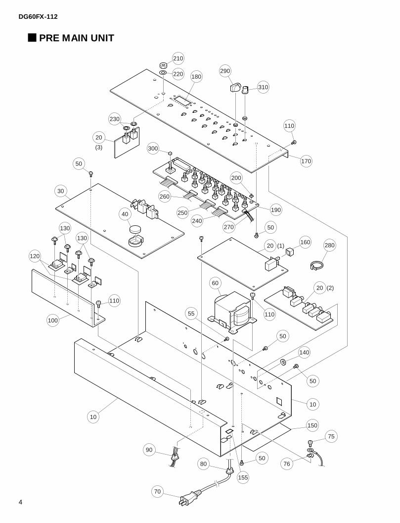
310
290180
210
220
230
20
(3) 300
260
250240
270 50
160
110
28020 (1)
60
40
20 (2)
50
55
50
30
110
100
130
120
50
10
10150
155
75
5080
90
70
76
140
190
170
110
200
130
PRE MAIN UNIT
DG60FX-112
5
: New Parts
REF NO. PART NO. DESCRIPTION REMARKS QTY RANK
******
***
*
***
Pre Main Unit J (V632220)Pre Main Unit C, U (V632230)Pre Main Unit H (V632240)Pre Main Unit B, S (V632250)
10 Chassis J10 Chassis C, U10 Chassis H, B20 Circuit Board Main J, U20 Circuit Board Main E30 Circuit Board DM40 Lithium Battery CR2450 0350 Bind Head Tapping Screw-B 3.0X8 MFZN2BL 18 0155 Bind Head Tapping Screw-P 3.0X12 MFZN2BL 3 0160 Power Transformer J60 Power Transformer UC60 Power Transformer H,BS70 AC Cord E H05VV-F3X0.75 6A E 0670 AC Cord BS H05VV-F3X0.75 B, S 0870 AC Cord UC SJT 3X#18 10A U, C 0670 AC Cord J VCTF 2X0.75 7A J 0575 Pan Head Screw SP 4.0X8 MFZN2Y 0176 Toothed Lock Washer-B 4.0 MFZN2BL 0180 Cord Strain Relief SR-5R1 0190 Cord Strain Relief SR-4N-4 0195 Glass Tube J (V704260)100 Heat Sink (V612570)110 Bind Head Tapping Screw-C A4.0X8 MFZN2BL 13 01120 Insulation Sheet UNISHEET T=0.15 2130 Bind Head Screw SP 3.0X12 MFZN2Y 4 01140 Hexagonal Nut 12.0 14X2 MFC2BL 4 01150 Insulation Sheet155 Insulation Sheet (S)160 Power Switch Knob 01170 Panel180 Meter Cover190 Circuit Board Front200 Button 17210 Hexagonal Nut 9.0 12X2 MFNI33 2 01220 Flat Washer 9X14 0.5 FNM3 2 01230 Toothed Lock Washer-A 9.0 MFZN2Y 2 01240 Connector Assembly C&C #28 12P L200 (V621630)250 Connector Assembly C&C #28 11P L200 (V621640)260 Connector Assembly C&C #28 9P L200 (V621650)270 Connector Assembly C&C #28 6P L400 (V621660)280 Cord Holder 6 01290 Knob (CH) 7 02300 Spacer310 Knob (FX) 8
--------
V6125400V6125500V6125600V6105800V6105900V6205300VS246400EP600190VC161100XZ082A00XZ083A00XZ084A00VV058200VV058300VV205600VZ461100EL200020ET900050VV103000CB072750
----
VC688900V3637600VB763800VD794100V6206500V4491100VU859000V6125100V5734500V6337500V5852100LX200060VL802300ET800150
--------
VV104600V3694100V5851800V5852300
RANK: Japan only
DG60FX-112
6
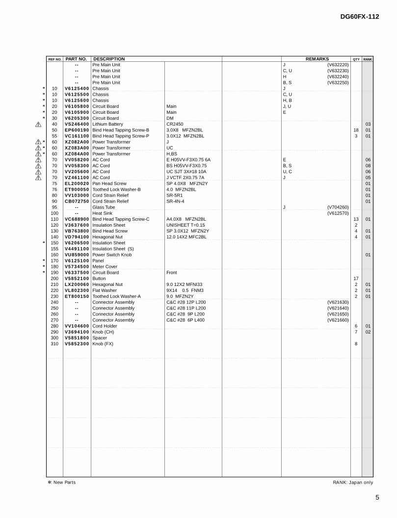
100
110
90
10
80
20
120
130
110
: New Parts
REF NO. PART NO. DESCRIPTION REMARKS QTY RANK
RANK: Japan only
Foot SW Overall Assembly J, U (V632200)Foot SW Overall Assembly H (V632210)
10 SW Top Cover20 LED Sheet80 Rear Sheet Assembly J, U80 Rear Sheet Assembly H90 Hexagonal Nut 9.0 12X2 MFNI33 01100 Flat Washer 9X14 0.5 FNM3 01110 Bind Head Tapping Screw-B 3.0X8 MFZN2BL 8 01120 SW Bottom Case130 Leg 4 01
----
V6145800V6337600V6337700V6337800LX200060VL802300EP600190V6145900VU859300
FOOT SWITCH OVERALL ASSEMBLY
****
*
DG60FX-112
7
: New Parts
REF NO. PART NO. DESCRIPTION REMARKS QTY RANK
RANK: Japan only
*******
*
**
**
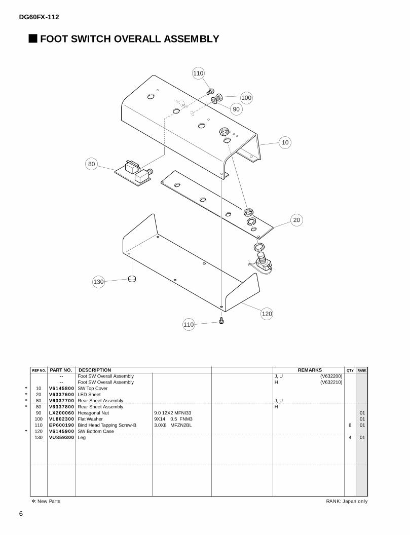
ELECTRICAL PARTS
ELECTRICAL PARTSCircuit Board DMCircuit Board MAIN(1/8-7/8) J, UCircuit Board MAIN(1/8-7/8) HCircuit Board REAR MAIN(8/8) J, UCircuit Board REAR MAIN(8/8) HCircuit Board FRONT PN 1/2Circuit Board SW,LED PN 2/2
Circuit Board DMIC Socket DICF-42CS-E 03
BT1 Battery Holder CR2450BH 03C1 Ceramic Cap. (chip) 0.1000 25V Z-9 Ceramic Cap. (chip) 0.1000 25V Z
C10 Electrolytic Cap. 100.00 16.0V 01C11 Ceramic Cap. (chip) 0.1000 25V Z-18 Ceramic Cap. (chip) 0.1000 25V ZC19 Electrolytic Cap. 100.00 16.0V 01C20 Ceramic Cap. (chip) 0.1000 25V Z-29 Ceramic Cap. (chip) 0.1000 25V ZC30 Electrolytic Cap. 10.00 35.0V 01C31 Ceramic Cap. (chip) 0.1000 25V ZC32 Ceramic Cap. (chip) 0.1000 25V ZC33 Electrolytic Cap. 10.00 35.0V 01C34 Ceramic Cap. (chip) 0.1000 25V ZC35 Ceramic Cap. (chip) 12P 50V JC36 Ceramic Cap. (chip) 12P 50V JC37 Electrolytic Cap. 100.00 16.0V 01C38 Ceramic Cap. (chip) 0.1000 25V Z-47 Ceramic Cap. (chip) 0.1000 25V ZC48 Electrolytic Cap. 100.00 16.0V 01C49 Ceramic Cap. (chip) 0.1000 25V Z-56 Ceramic Cap. (chip) 0.1000 25V ZC57 Ceramic Cap. (chip) 0.0100 50V KC58 Ceramic Cap. (chip) 0.0100 50V KC59 Ceramic Cap. (chip) 0.1000 25V Z-71 Ceramic Cap. (chip) 0.1000 25V ZC72 Electrolytic Cap. 220.00 25.0V 01C73 Ceramic Cap. (chip) 0.1000 25V ZC74 Ceramic Cap. (chip) 220P 50V JC75 Ceramic Cap. (chip) 0.0100 50V KC76 Ceramic Cap. (chip) 0.0100 50V KC77 Ceramic Cap. (chip) 0.1000 25V ZC78 Ceramic Cap. (chip) 0.1000 25V ZC79 Ceramic Cap. (chip) 0.0100 50V KC105 Electrolytic Cap.-BP 10.00 35.0VC106 Ceramic Cap. (chip) 10P 50V DC107 Ceramic Cap. (chip) 0.1000 25V ZC108 Ceramic Cap. (chip) 0.1000 25V ZC109 Ceramic Cap. (chip) 22P 50V JC110 Ceramic Cap. (chip) 1000P 50V KC111 Electrolytic Cap.-BP 10.00 35.0VC112 Ceramic Cap. (chip) 68P 50V JC113 Ceramic Cap. (chip) 22P 50V JC114 Ceramic Cap. (chip) 1000P 50V KC115 Electrolytic Cap. 10.00 35.0V 01C116 Ceramic Cap. (chip) 0.1000 25V ZC119 Electrolytic Cap. 10.00 35.0V 01-122 Electrolytic Cap. 10.00 35.0V 01C123 Ceramic Cap. (chip) 0.1000 25V ZC124 Ceramic Cap. (chip) 0.1000 25V ZC125 Electrolytic Cap. 10.00 35.0V 01C126 Electrolytic Cap. 10.00 35.0V 01C127 Ceramic Cap. (chip) 0.1000 25V ZC128 Ceramic Cap. (chip) 0.1000 25V ZC129 Electrolytic Cap. 10.00 35.0V 01C130 Electrolytic Cap.-BP 10.00 35.0VC131 Electrolytic Cap.-BP 10.00 35.0VC156 Electrolytic Cap. 100.00 25.0V 01C157 Ceramic Cap. (chip) 0.1000 25V Z
V6205300V6105800V6105900V6337700V6337800V6337500V6337600
V6205300VK863100VS246300UX145100UX145100UR838100UX145100UX145100UR838100UX145100UX145100UR857100UX145100UX145100UR857100UX145100UX061120UX061120UR838100UX145100UX145100UR838100UX145100UX145100UX064100UX064100UX145100UX145100UR848220UX145100UX062220UX064100UX064100UX145100UX145100UX064100V6197100UX061100UX145100UX145100UX061220UX063100V6197100UX061680UX061220UX063100UR857100UX145100UR857100UR857100UX145100UX145100UR857100UR857100UX145100UX145100UR857100V6197100V6197100UR848100UX145100
DG60FX-112
8
: New Parts
REF NO. PART NO. DESCRIPTION REMARKS QTY RANK
RANK: Japan only
C158 Ceramic Cap. (chip) 0.1000 25V ZC159 Electrolytic Cap. 100.00 25.0V 01C160 Ceramic Cap. (chip) 0.1000 25V Z-188 Ceramic Cap. (chip) 0.1000 25V ZC189 Electrolytic Cap. 100.00 25.0V 01C190 Electrolytic Cap. 100.00 25.0V 01C191 Ceramic Cap. (chip) 5P 50V CC192 Ceramic Cap. (chip) 5P 50V CC193 Ceramic Cap. (chip) 0.1000 25V Z-197 Ceramic Cap. (chip) 0.1000 25V ZC200 Ceramic Cap. (chip) 0.1000 25V Z-209 Ceramic Cap. (chip) 0.1000 25V ZCN1 Connector Base Post M2426XX 12P TE 01CN2 Connector Base Post M2426XX 11P TE 01CN3 Connector Base Post M2426XX 9P TE 01CN4 Connector Base Post M24185XX 4P TE
CN101 Connector Base Post M2426XX 2P TE 01CN102 Connector Base Post M2426XX 3P TE 01CN103 Connector Base Post M2426XX 6P TE 01CN104 Connector Base Post M24185XX 3P TE
D1 Diode 1SS355 TE-17 01D103 Diode 1SS355 TE-17 01D104 Diode 1SS355 TE-17 01IC1 IC MX23C8100PC-10 8M ROMIC2 IC W24258S-70LE-EL10 256K 07IC2 IC CY62256LL-70SNCT 256K 05IC3 IC W24258S-70LE-EL10 256K 07IC3 IC CY62256LL-70SNCT 256K 05IC4 IC MB3790PF ASSP 05IC5 IC 74AHC32DT ORIC6 IC 74AHC32DT ORIC7 IC 74HC08DT ANDIC8 IC YSS910-S DSP6 10IC9 IC YSS910-S DSP6 10IC10 IC MSM514260C-60JS 4M 07IC10 IC SDM4260CLU-6S 4M 08IC11 IC MSM514260C-60JS 4M 07IC11 IC SDM4260CLU-6S 4M 08IC12 IC HD6413002FP16 CPU 09IC13 Photo Coupler PC410T 04IC13 Photo Coupler HCPL-M600 04IC14 IC 74HC244DT BUS BUF-16 IC 74HC244DT BUS BUF
IC17 IC YM3437C-F DIT2 07IC18 IC UPC29M33T-E1 3.3V 03IC102 IC NJM5532M OP AMP 03IC103 IC NJM5532M OP AMP 03IC104 IC AK4520A-VF-E2 ADC & DAC 07IC107 IC 74HCU04DT INVERTORIC108 IC TC74HC4040F B. COUNTER 03IC109 IC 74HC164DT SHIFT RESISTIC110 IC 74HC175DT D-FFIC111 IC NJM78M05DLA 5.0V REGULATORJK1 DIN Connector 5P3 HDC-052AJK2 Pin Connector HSP-241V1BJ1 Jumper Wire 0.55 (VA07890)J2 Jumper Wire 0.55 (VA07890)J3 Jumper Wire 0.55 (VA07890)L1 Chip Inductance BLM21B751S 03-4 Chip Inductance BLM21B751S 03L7 Pulse Transformer TC-1019-06 04L8 Noise Filter ZJYS51R5-2PTL9 Chip Inductance BLM21B751S 03R1 Carbon Resistor (chip) 10K 0.1 JR2 Carbon Resistor (chip) 100 0.1 J-8 Carbon Resistor (chip) 100 0.1 JR9 Carbon Resistor (chip) 270 0.1 JR10 Carbon Resistor (chip) 10K 0.1 JR11 Carbon Resistor (chip) 10K 0.1 JR12 Carbon Resistor (chip) 1.0K 0.1 J
UX145100UR848100UX145100UX145100UR848100UR848100UX060500UX060500UX145100UX145100UX145100UX145100VV067200VV067100VV066900V3764200VV066200VV066300VV066600V3764100VT332900VT332900VT332900XZ198100XV411A00XW433A00XV411A00XW433A00XR967A00XZ103A00XZ103A00XZ108A00XV988A00XV988A00XV077A00XV839A00XV077A00XV839A00XQ375A00VN686000VR903700XZ109A00XZ109A00XM530A00XU965A00XC011A00XC011A00XT802A00XZ110A00XR684A00XZ112A00XZ113A00XZ162A00V6177500V6178000
------
VS740100VS740100VC548200V6178900VS740100RG007100RG005100RG005100RG005270RG007100RG007100RG006100
**
*
*
*
*
DG60FX-112
9
: New Parts
REF NO. PART NO. DESCRIPTION REMARKS QTY RANK
RANK: Japan only
R13 Carbon Resistor (chip) 220 0.1 JR14 Carbon Resistor (chip) 10K 0.1 J-16 Carbon Resistor (chip) 10K 0.1 JR17 Carbon Resistor (chip) 2.2K 0.1 JR18 Carbon Resistor (chip) 220 0.1 JR19 Carbon Resistor (chip) 220 0.1 JR22 Carbon Resistor (chip) 1.0M 0.1 JR23 Carbon Resistor (chip) 47 0.1 JR24 Carbon Resistor (chip) 75 0.1 JR26 Carbon Resistor (chip) 10K 0.1 JR27 Carbon Resistor (chip) 0 0.1 JR29 Carbon Resistor (chip) 1.0K 0.1 JR107 Carbon Resistor (chip) 100K 0.1 JR108 Carbon Resistor (chip) 10K 0.1 FR109 Carbon Resistor (chip) 22K 0.1 FR110 Carbon Resistor (chip) 3.3K 0.1 FR111 Carbon Resistor (chip) 10K 0.1 JR112 Carbon Resistor (chip) 10K 0.1 JR113 Carbon Resistor (chip) 5.6K 0.1 JR114 Carbon Resistor (chip) 5.6K 0.1 JR115 Carbon Resistor (chip) 470 0.1 JR116 Carbon Resistor (chip) 470 0.1 JR117 Carbon Resistor (chip) 10K 0.1 FR118 Carbon Resistor (chip) 470 0.1 FR119 Carbon Resistor (chip) 2.7K 0.1 FR120 Carbon Resistor (chip) 5.6K 0.1 JR121 Carbon Resistor (chip) 5.6K 0.1 JR122 Carbon Resistor (chip) 470 0.1 JR123 Carbon Resistor (chip) 470 0.1 JR124 Carbon Resistor (chip) 4.7K 0.1 JR125 Carbon Resistor (chip) 33 0.1 JR126 Carbon Resistor (chip) 4.7K 0.1 JR127 Carbon Resistor (chip) 4.7 1/4 JR128 Carbon Resistor (chip) 1.0K 0.1 JR130 Carbon Resistor (chip) 1.0K 0.1 JR163 Carbon Resistor (chip) 1.0M 0.1 JR164 Carbon Resistor (chip) 680 0.1 JR165 Carbon Resistor (chip) 220 0.1 JRA1 Resistor Array 10KX4-18 Resistor Array 10KX4TR1 Transistor 2SC2412K Q,R,S 01TR2 Transistor 2SC2412K Q,R,S 01X1 Quartz Crystal Unit 30.00M HZ DOC-49S2 06X2 Quartz Crystal Unit AT-49/12.0000MHZ 03
X101 Quartz Crystal Unit 24.576M AF3817CQA 03ZD101 Zener Diode UDZ 2.0BTE-17 2.0VZD102 Zener Diode UDZ 2.0BTE-17 2.0V
Circuit Board ANALOG J, U (V633730)Circuit Board ANALOG E (V633740)Circuit Board MAIN(1/8-7/8) J, UCircuit Board MAIN(1/8-7/8) HCircuit Board REAR MAIN8/8 J, UCircuit Board REAR MAIN8/8 HJumper Wire 0.60 (VV29140) 20 01Fuse Holder CQ-05CT 8 01
BT601 Connector Assembly #18 2P L 300C401 Monolithic Mylar Capacitor 0.22 50V J 01C402 Ceramic Capacitor-SL 100P 50V J 01C403 Electrolytic Cap. 10.00 25.0V 01C404 Monolithic Mylar Capacitor 0.22 50V J 01C406 Ceramic Capacitor-SL 100P 50V J 01C407 Electrolytic Cap. 10.00 25.0V 01C408 Electrolytic Cap. 10.00 25.0V 01C409 Ceramic Capacitor-SL 100P 50V J 01C410 Electrolytic Cap. 4.70 50.0V 01C411 Mylar Capacitor 0.1 50V J 01C412 Electrolytic Cap. 10.00 25.0V 01C413 Electrolytic Cap. 10.00 25.0V 01C501 Electrolytic Cap. 10.00 25.0V 01
RG005220RG007100RG007100RG006220RG005220RG005220RG009100RG004470RG004750RG007100RG000000RG006100RG008100RG107100RG107220RG106330RG007100RG007100RG006560RG006560RG005470RG005470RG107100RG105470RG106270RG006560RG006560RG005470RG005470RG006470RG004330RG006470RG203470RG006100RG006100RG009100RG005680RG005220RH047100RH047100VV556400VV556400VU682100VE463500VN277000VU170900VU170900
----
V6105800V6105900V6337700V6337800
--VV319600V3632400VV321100VZ353500UR847100VV321100VZ353500UR847100UR847100VZ353500UR866470VV062800UR847100UR847100UR847100
**
***
***********
*
*
**
****
DG60FX-112
10
: New Parts
REF NO. PART NO. DESCRIPTION REMARKS QTY RANK
RANK: Japan only
C502 Electrolytic Cap. 10.00 25.0V 01C503 Ceramic Capacitor-SL 100P 50V J 01C504 Electrolytic Cap. 47.00 25.0V 01C505 Electrolytic Cap. 10.00 25.0V 01C506 Electrolytic Cap. 10.00 25.0V 01C507 Ceramic Capacitor-SL 100P 50V J 01C508 Electrolytic Cap. 47.00 25.0V 01C509 Ceramic Cap.-B 1000P 50V K 01C510 Electrolytic Cap. 10.00 25.0V 01-512 Electrolytic Cap. 10.00 25.0V 01C513 Ceramic Cap.-B 1000P 50V K 01C514 Electrolytic Cap. 10.00 25.0V 01-516 Electrolytic Cap. 10.00 25.0V 01C517 Ceramic Capacitor-SL 100P 50V J 01C518 Electrolytic Cap. 10.00 25.0V 01C519 Electrolytic Cap. 10.00 25.0V 01C520 Monolithic Ceramic Cap. 0.10 50V Z 01-525 Monolithic Ceramic Cap. 0.10 50V Z 01C601 Capacitor 0.01 400V J.U.C.S 02C602 Electrolytic Cap. 1.00 50.0V 01C603 Electrolytic Cap. 4.70 50.0V 01C604 Polypropylene Capacitor 0.022U/250VC605 Polypropylene Capacitor 0.022U/250VC606 Electrolytic Cap. -LP 3300U 50V SNAP INC607 Electrolytic Cap. -LP 3300U 50V SNAP INC608 Electrolytic Cap. 10.00 25.0V 01C609 Electrolytic Cap. 10.00 25.0V 01C610 Ceramic Capacitor-F 0.0100 50V Z 01C611 Ceramic Capacitor-F 0.0100 50V Z 01C612 Monolithic Ceramic Cap. 0.10 50V Z 01C613 Electrolytic Cap. 2200 16.0VC614 Electrolytic Cap. 2200 16.0VC615 Ceramic Capacitor-F 0.0100 50V Z 01C616 Ceramic Capacitor-F 0.0100 50V Z 01C617 Electrolytic Cap. 10.00 25.0V 01C618 Electrolytic Cap. 1.00 50.0V 01C619 Ceramic Cap.-B 1000P 50V K 01C620 Electrolytic Cap. 47.00 50.0V 01-622 Electrolytic Cap. 47.00 50.0V 01C623 Ceramic Capacitor-SL 100P 50V J 01C624 Ceramic Cap.-B 220P 50V K 01C625 Ceramic Cap.-B 220P 50V K 01C626 Electrolytic Cap. 100.00 35.0V 01C627 Mylar Capacitor 0.1 50V J 01C628 Mylar Capacitor 0.1 50V J 01C629 Monolithic Ceramic Cap. 0.10 50V Z 01C630 Monolithic Ceramic Cap. 0.10 50V Z 01C701 Monolithic Ceramic Cap. 0.10 50V Z 01C702 Monolithic Ceramic Cap. 0.10 50V Z 01
CN401 Connector Base Post M24185XX 3P TECN601 Base Post Connector VA- 2P TE 01CN602 Base Post Connector VH- 4P TE 01CN603 Base Post Connector VH- 5P TE 01CN607 Connector Base Post M2426XX 2P TE 01D401 Diode 1SS133,176,HSS104 01-405 Diode 1SS133,176,HSS104 01D601 Diode 1SS82TD 01D602 Diode 1SS133,176,HSS104 01
DB601 Diode Stack PBU403 4.0A 200V 03DB602 Diode Stack S1VB20 1.0A 200V 02FT601 FET 2SK30ATM Y 03FZ601 Fuse TDS 2A 250V J/U/C 01-603 Fuse TDS 2A 250V J/U/C 01
FZ604 Fuse TDS 1A 250V J/U/C 01IC401 IC NJM072D OP AMP 04IC402 IC NJM072D OP AMP 04IC501 IC NJM4556AD OP AMP 02IC502 IC NE5532P OP AMP 06IC601 IC NJM7805FA 5V REGULATOR 02JK401 Phone Jack HTJ-064-12I
UR847100VZ353500UR847470UR847100UR847100VZ353500UR847470VZ353900UR847100UR847100VZ353900UR847100UR847100VZ353500UR847100UR847100VZ354600VZ354600VV520600UR866100UR866470V3632700V3632700V3632800V3632800UR847100UR847100VZ354000VZ354000VZ354600UR639220UR639220VZ354000VZ354000UR847100UR866100VZ353900UR867470UR867470VZ353500VZ353600VZ353600UR858100VV062800VV062800VZ354600VZ354600VZ354600VZ354600V3764100VG879900LB932040LB932050VV066200VD631600VD631600I F 0 0 5 5 6 0VD631600VV518200VQ379300I E 0 0 0 0 1 0VV070600VV070600VV070300IG107000IG107000XQ824A00IG102500XJ607A00V3633400
**
**
*
DG60FX-112
11
: New Parts
REF NO. PART NO. DESCRIPTION REMARKS QTY RANK
RANK: Japan only
JK402 Phone Jack HTJ-064-12IJK501 Phone Jack HTJ-064 02-503 Phone Jack HTJ-064 02
JK504 Phone Jack HTJ-064-05BJK505 DIN Connector TCS5094-10-4151 04JK701 Phone Jack STEREO HTJ-064-12DJK702 DIN Connector TCS5094-10-4151 04K501 Terminal Plate 01K502 Terminal Plate 01
LD401 LED RED LT311G-41-C13 01R401 Carbon Resistor 10.0K 1/4 J 01R402 Carbon Resistor 1.0M 1/4 J 01R403 Carbon Resistor 4.7K 1/4 J 01R404 Carbon Resistor 27.0K 1/4 J 01R405 Carbon Resistor 10.0K 1/4 J 01R406 Carbon Resistor 10.0K 1/4 J 01R407 Carbon Resistor 1.0M 1/4 J 01R408 Carbon Resistor 4.7K 1/4 J 01R409 Carbon Resistor 4.7K 1/4 J 01R410 Carbon Resistor 10.0K 1/4 J 01R411 Carbon Resistor 10.0K 1/4 J 01R412 Carbon Resistor 4.7K 1/4 J 01R413 Carbon Resistor 100.0 1/4 J 01R414 Carbon Resistor 1.0K 1/4 J 01R415 Carbon Resistor 10.0K 1/4 J 01-418 Carbon Resistor 10.0K 1/4 J 01R419 Carbon Resistor 1.2K 1/4 J 01R420 Carbon Resistor 100.0K 1/4 J 01R421 Carbon Resistor 1.0K 1/4 J 01R501 Carbon Resistor 1.0K 1/4 J 01R502 Carbon Resistor 1.0K 1/4 J 01R503 Carbon Resistor 220.0K 1/4 J 01R504 Carbon Resistor 1.0K 1/4 J 01R505 Carbon Resistor 10.0K 1/4 J 01R506 Carbon Resistor 4.7K 1/4 J 01R507 Carbon Resistor 4.7K 1/4 J 01R508 Carbon Resistor 100.0K 1/4 J 01R509 Carbon Resistor 1.0K 1/4 J 01R510 Carbon Resistor 10.0K 1/4 J 01R511 Carbon Resistor 4.7K 1/4 J 01R512 Carbon Resistor 4.7K 1/4 J 01R513 Carbon Resistor 100.0 1/4 J 01R514 Carbon Resistor 100.0 1/4 J 01-516 Carbon Resistor 10.0K 1/4 J 01R517 Carbon Resistor 220.0K 1/4 J 01R518 Carbon Resistor 6.8K 1/4 J 01R519 Carbon Resistor 22.0K 1/4 J 01R520 Carbon Resistor 100.0 1/4 J 01R521 Carbon Resistor 100.0 1/4 J 01R522 Carbon Resistor 100.0K 1/4 J 01R523 Carbon Resistor 2.2K 1/4 J 01R524 Carbon Resistor 100.0K 1/4 J 01R525 Carbon Resistor 100.0 1/4 J 01R526 Carbon Resistor 10.0K 1/4 J 01R527 Carbon Resistor 100.0K 1/4 J 01R601 Carbon Resistor 10.0K 1/4 J 01R602 Carbon Resistor 100.0K 1/4 J 01R603 Carbon Resistor 22.0K 1/4 J 01R604 Carbon Resistor 100.0K 1/4 J 01R605 Carbon Resistor 2.2K 1/4 J 01R606 Carbon Resistor 100.0K 1/4 J 01R607 Carbon Resistor 100.0K 1/4 J 01R608 Carbon Resistor 4.7K 1/4 J 01R609 Carbon Resistor 4.7K 1/4 J 01R610 Metal Oxide Film Resistor 2.2K 3W JR611 Metal Oxide Film Resistor 180 5W J-614 Metal Oxide Film Resistor 180 5W JR615 Carbon Resistor 2.2K 1/4 J 01R616 Carbon Resistor 10.0K 1/4 J 01R617 Carbon Resistor 56.0K 1/4 J 01
V3633400VV278300VV278300V6176500VR309600V6177700VR309600VV075700VV075700VV620800HF457100HF459100HF456470HF457270HF457100HF457100HF459100HF456470HF456470HF457100HF457100HF456470HF455100HF456100HF457100HF457100HF456120HF458100HF456100HF456100HF456100HF458220HF456100HF457100HF456470HF456470HF458100HF456100HF457100HF456470HF456470HF455100HF455100HF457100HF458220HF456680HF457220HF455100HF455100HF458100HF456220HF458100HF455100HF457100HF458100HF457100HF458100HF457220HF458100HF456220HF458100HF458100HF456470HF456470V3633200V3751900V3751900HF456220HF457100HF457560
*
DG60FX-112
12
: New Parts
REF NO. PART NO. DESCRIPTION REMARKS QTY RANK
RANK: Japan only
*
*
*
***
R618 Carbon Resistor 470.0 1/4 J 01R619 Carbon Resistor 12.0K 1/4 J 01R620 Carbon Resistor 1.0K 1/4 J 01R621 Carbon Resistor 1.5K 1/4 J 01R622 Carbon Resistor 56.0K 1/4 J 01R623 Carbon Resistor 1.0K 1/4 J 01R624 Carbon Resistor 3.3K 1/4 J 01R625 Carbon Resistor 5.6K 1/4 J 01R626 Carbon Resistor 3.3K 1/4 J 01R627 Carbon Resistor 1.0K 1/4 J 01R628 Carbon Resistor 2.2K 1/4 J 01-630 Carbon Resistor 220.0 1/4 J 01R631 Carbon Resistor 330.0 1/4 J 01R632 Carbon Resistor 330.0 1/4 J 01R633 Flame Proof C. Resistor 100 1/4 J 01R634 Wire Wound Resistor 0.33 5W JR635 Wire Wound Resistor 0.33 5W JR636 Metal Oxide Film Resistor 4.7 1W JR637 Wire Wound Resistor 0.33 5W JR701 Carbon Resistor 1.0K 1/4 J 01
SW601 Push Switch SDDLB11874-YL 03TR401 Transistor 2SC1815 Y,GR 01TR501 Transistor 2SC2878 A,B 01TR502 Transistor 2SC2878 A,B 01TR601 Transistor 2SC1815 Y,GR 01TR602 Transistor 2SA1015 O,Y 01TR603 Transistor 2SC2878 A,B 01TR604 Transistor 2SA970 GR,BL 01TR605 Transistor 2SA970 GR,BL 01TR606 Transistor 2SC2705 O,Y 01TR607 Transistor 2SC3421 O,Y 02TR608 Transistor 2SA1358 O,Y 02TR609 Pair Transistor A1492(Z)/C3856(Z)TR610 Transistor 2SC3421 O,Y 02VR601 Trimmer Potentiometer B 1K TB655MCW401 Connector Assembly B&C #28 2P L 150 (V620350)W501 Connector Assembly B&B #24 5P L 150 (V620380)W502 Connector Assembly B&C #26 3P L 350 (V620340)W503 Connector Assembly B&C #28 14P L 200 (V621760)W601 Connector Assembly B&B #24 3P L 200 (V363250)W603 Connector Assembly B&C #24 4P L 150 (V620370)W604 Connector Assembly B&B #24 3P L 200 (V363250)W606 Connector Assembly B&B #26 3P L 150 (V620410)W608 Connector Assembly B&B #24 3P L 200 (V363250)W610 Connector Assembly B&C #24 3P L 130 (V363210)W611 Connector Assembly B&C #24 3P L 300 (V620360)W701 Connector Assembly B&C #28 14P L 100 (V620390)ZD601 Zener Diode MTZ J 15.0B 15.0V 01ZD602 Zener Diode MTZ J 15.0B 15.0V 01ZD603 Zener Diode 3Z15 15V 3WZD604 Zener Diode 3Z15 15V 3W
Circuit Board PN (V620230)Circuit Board FRONT PN 1/2Circuit Board SW,LED PN 2/2SW Spacer 8LED Holder LED3-1A 6Connector Assembly #24 2P L60 (V654510) 4Push Switch ADS-003-A10 4
C301 Ceramic Cap. (chip) 0.1000 25V Z-315 Ceramic Cap. (chip) 0.1000 25V Z
CN301 Connector Base Post M2426XXR 6P SE 01CN302 Connector Base Post M2426XXR 9P SE 01CN303 Connector Base Post M2426XXR 11P SECN304 Connector Base Post M2426XXR 12P SE 01CN305 Connector Base Post M2426XXR 14P SE 01CN306 Connector Base Post M2426XX 14P TECN307 Connector Base Post M2426XX 2P TE 01-310 Connector Base Post M2426XX 2P TE 01D301 Diode 1SS355 TE-17 01
HF455470HF457120HF456100HF456150HF457560HF456100HF456330HF456560HF456330HF456100HF456220HF455220HF455330HF455330VV276800V4480100V4480100V3632900V4480100HF456100VV059400IC1815M0IC287820IC287820IC1815M0IA101590IC287820IA097030IA097030VE198800IC342100IA135800VV597200IC342100V3633500
------------------------
VG440800VG440800V3752000V3752000
--V6337500V6337600V6220800V6624600
--V6124500UX145100UX145100VV068000VV068300VV068500VV068600VV068800VV067400VV066200VV066200VT332900
DG60FX-112
13
: New Parts
REF NO. PART NO. DESCRIPTION REMARKS QTY RANK
RANK: Japan only
-322 Diode 1SS355 TE-17 01IC301 IC 74HC374DT D-FF-307 IC 74HC374DT D-FF
IC308 IC 74HC4052DT MULTIPLEXERIC309 IC 74HC4052DT MULTIPLEXERLD301 LED Display LTC-5836ELD302 LED RED LT311G-41-C13 01-307 LED RED LT311G-41-C13 01L301 Chip Inductance BLM21B751S 03-312 Chip Inductance BLM21B751S 03R301 Carbon Resistor (chip) 10K 0.1 J-304 Carbon Resistor (chip) 10K 0.1 JR305 Carbon Resistor (chip) 560 0.1 J-321 Carbon Resistor (chip) 560 0.1 JR322 Carbon Resistor (chip) 820 0.1 J-345 Carbon Resistor (chip) 820 0.1 JR346 Carbon Resistor (chip) 10K 0.1 J-360 Carbon Resistor (chip) 10K 0.1 JR361 Carbon Resistor (chip) 1.0K 0.1 J-367 Carbon Resistor (chip) 1.0K 0.1 JR368 Carbon Resistor (chip) 10K 0.1 JR369 Carbon Resistor (chip) 10K 0.1 JR370 Carbon Resistor (chip) 560 0.1 J-375 Carbon Resistor (chip) 560 0.1 J
SW301 Push Switch SKHQFN GREEN 02-317 Push Switch SKHQFN GREEN 02
SW318 Rotary Switch SRBV18 1C-8S 07VR301 Rotary Variable Resistor RK09L1140 10KB-313 Rotary Variable Resistor RK09L1140 10KB
VR314 Rotary Variable Resistor RK09L12D0 20KA X2
VT332900XZ102A00XZ102A00XZ101A00XZ101A00V5801000VV620800VV620800VS740100VS740100RG007100RG007100RG005560RG005560RG005820RG005820RG007100RG007100RG006100RG006100RG007100RG007100RG005560RG005560VK701100VK701100V3633800V5264800V5264800V5265100
L
K
J
I
H
G
F
E
D
C
B
A
1 2 3 4 5 6 7 8 9 10 11 12
DG60FX-112
M
N
O
P
Q
1 2 3 4 5 6 7 8 9 10 11 12
Q
P
O
N
M
L
K
J
I
H
G
F
E
D
C
B
A
DG60FX-112DG60FX-112
Note : See parts list for details of circuit board component parts.
KEC-54205 2
DG60FX-112 OVERALL CIRCUIT DIAGRAM 1/2(DM)
KEC-54205
: Mylar Capacitor
: Ceramic Capacitor
: Flame Proof C.
to MAIN 2/8 -W502
to FRONT-CN301
-CN304
-CN303
to FRONT
to FRONT
to FRONT-CN302
-W603to MAIN 1/8
8M ROM256K RAM 256K RAM
OR OR OR OR
OR
ASSP
AND
OR
OR
AND
to MAIN 1/8-W610
CPU
DSP6
DSP6
PHOTO COUPLER
BUFFER
BUFFER
BUFFER
PULSE TRANSFORMER
INVERTER
4M DRAM
4M DRAM
DIT2
3.3V REGULATOR
ADC & DACto MAIN 3/8 -W401
5.0V REGULATOR
B. COUNTER
SHIFTREGIST
D-FF
INVERTER
OP AMP OP AMP
OP AMPOP AMP
REGULATOR +3.3V
UPC29M33T-E1 (XU965A00)
1
DM: IC18
33
2: GND1: V IN
3: OUTPUT2: GND1: INPUT
3: OUTPUT
NJM78M05DLA
REGULATOR +5VDM: IC111
2
(XZ162A00)
1
2
3
2: GND1: INPUT
3: OUTPUT
NJM7805FA (XJ607A00)
REGULATOR +5V
21
DM: IC112
MX23C8100PC-10
DIGITALOUT
: Metal Oxide Film Resistor
: Wire Wound Resistor
DM
L
K
J
I
H
G
F
E
D
C
B
A
1 2 3 4 5 6 7 8 9 10 11 12
DG60FX-112
M
N
O
P
Q
1 2 3 4 5 6 7 8 9 10 11 12
Q
P
O
N
M
L
K
J
I
H
G
F
E
D
C
B
A
DG60FX-112DG60FX-112
DG60FX-112 OVERALL CIRCUIT DIAGRAM 2/2(FRONT, MAIN 1/8, 2/8, 3/8, 4/8, 5/8, 6/8, 7/8, REAR)
KEC-54204 1
D-FF D-FF
D-FFD-FF
D-FFD-FF
D-FF
to DM-CN103
MULTIPLEXER
to DM-CN3
MULTIPLEXER
to DM-CN1 to DM-CN2
3/8
POWERTRANSFORMER
POWERCODE
CODEBUSH
to DM-CN101
OP AMP OP AMP
OP AMP
OP AMP
1/8
to DM-CN104
DIODE STACK
to DM-CN4
DIODE BRIDGE
POWER TRANSFORMER
4/8
5V REGULATOR
7/8
SPEAKER
N.C
6/8
5/8
OP AMP
to PN1/2-CN305
to DM-CN102
OP AMP
OP AMP
OP AMP
2/8
to SW, LED-CN306
FOOT SW1 FOOT SW2 FOOT SW3 FOOT SW BANK
to MAIN2/8-W503
AMP SELECTGAIN MASTER TREBLE REVERBSPEEDPRESENCEMIDDLE BASS COMP DEPTH TIME FEEDBACK LEVEL
DE
LAY
TR
EM
OLO
RO
TA
RY
PH
AS
ER
SP
.S
IM
SP
RIN
G
TA
PE
EC
HO
PLA
TE
HA
LLC
HO
RU
S
ST
OR
E
CO
MP
UP
DO
WN
FLA
NG
ER
MA
NU
AL
UT
ILIT
Y
(PN 1/2)
(ANALOG 8/8)
KEC-54206 1
KEC-54206 1
KEC-54206 1
KEC-54206 1
KEC-54206 1
EXP. PEDAL
(PN 2/2)
KEC-54206 1
DESTINATION
DESTINATION
KEC-54206 1
W611W610
W501W612
W502
W503
1KEC-54206
BL
WH
BL
WHGR
BR
BUGR/YE
BR
BUGR/YE
100
100K
HTJ-064-05B
Foot Switch Unit
C520
C521
C523
C522
C525
C524
toR
EA
R-W
701
22K
6.8K
FRONT
MAIN
MAIN
MAIN
MAIN
MAIN
MAIN
MAIN REAR
SW, LED

![Untitled-3 [] · YAMAHA YAMAHA OYAMAHA eVS our YAMÁHA . YAMAHA YAMAHA . Title: Untitled-3 Created Date: 11/26/2019 4:37:47 PM](https://img.pdfslide.us/doc/110x75/5f2e302990a8313a801edc68/untitled-3-yamaha-yamaha-oyamaha-evs-our-yamha-yamaha-yamaha-title-untitled-3.jpg)