Embed Size (px)
Citation preview

SERVICE MANUAL
100 Hz Chassis28 CTV“
100 Hz. Chassis 28” Service Manual
3
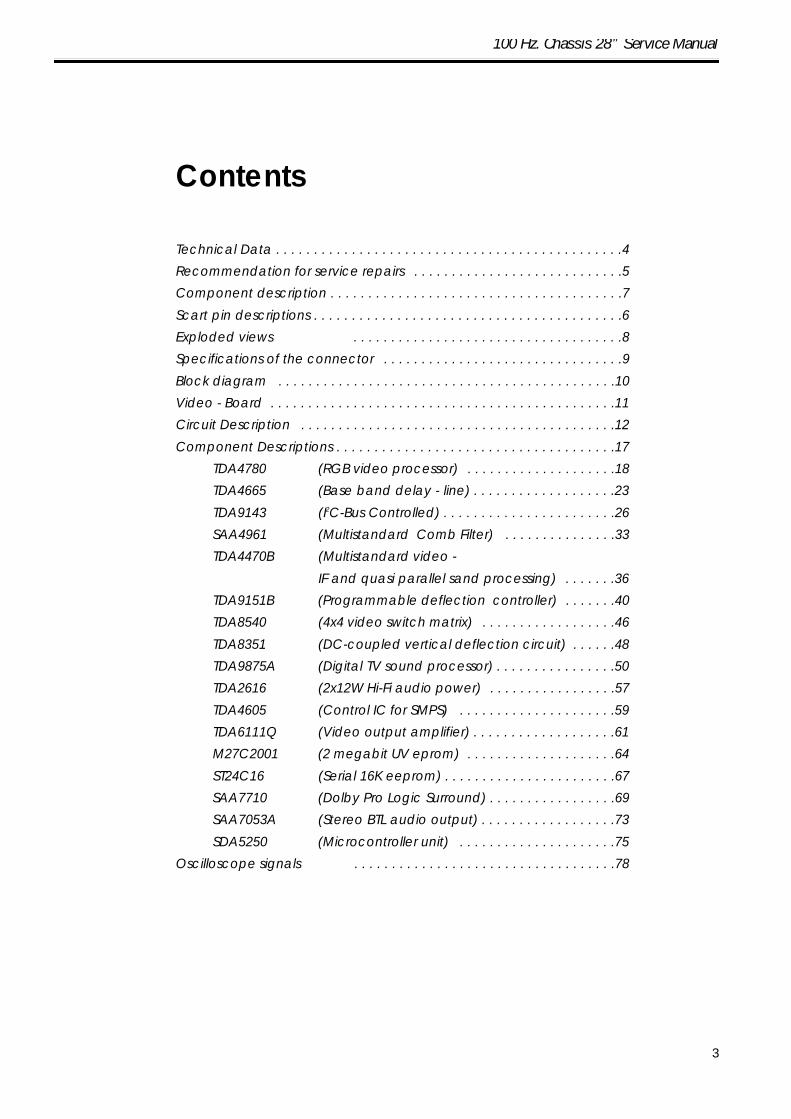
Contents
Technical Data . . . . . . . . . . . . . . . . . . . . . . . . . . . . . . . . . . . . . . . . . . . . . .4
Recommendation for service repairs . . . . . . . . . . . . . . . . . . . . . . . . . . . .5
Component description . . . . . . . . . . . . . . . . . . . . . . . . . . . . . . . . . . . . . . .7
Scart pin descriptions . . . . . . . . . . . . . . . . . . . . . . . . . . . . . . . . . . . . . . . . .6
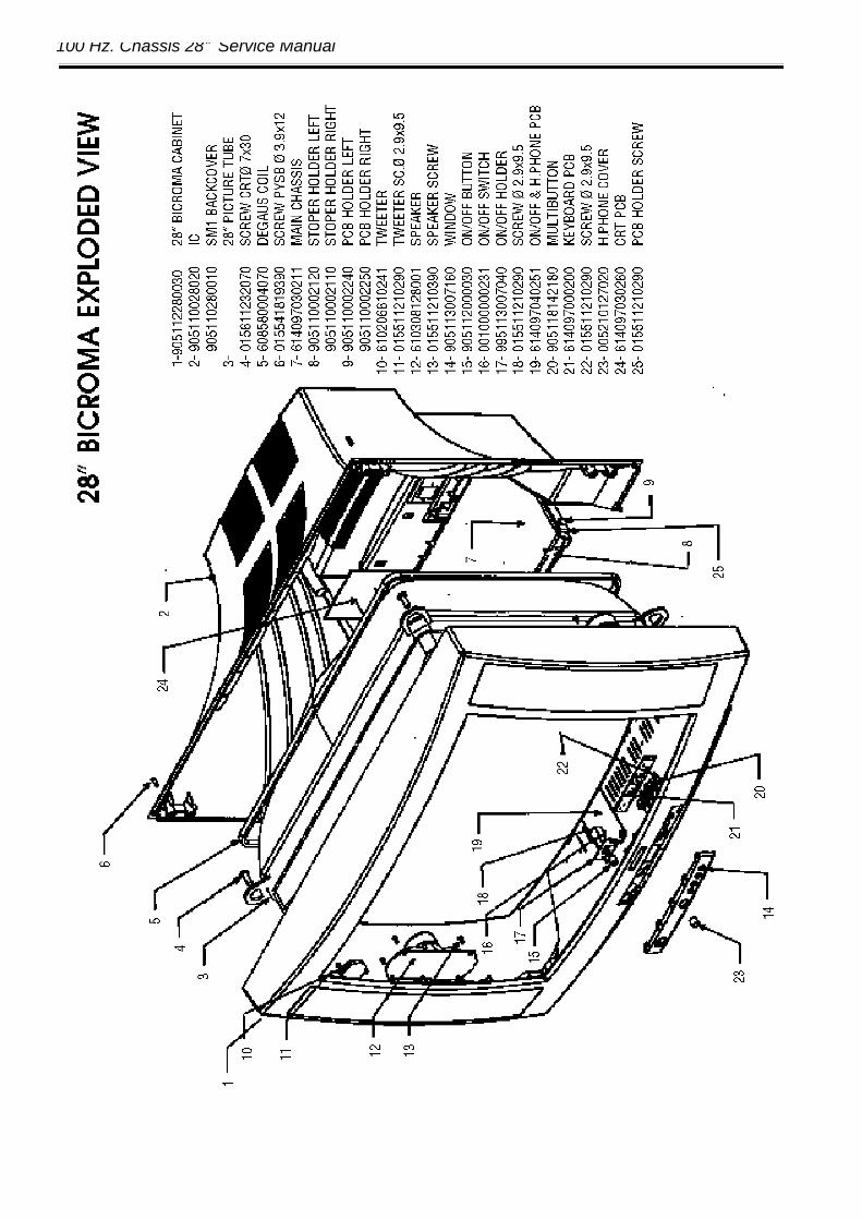
Exploded views . . . . . . . . . . . . . . . . . . . . . . . . . . . . . . . . . . . .8
Specifications of the connector . . . . . . . . . . . . . . . . . . . . . . . . . . . . . . . .9
Block diagram . . . . . . . . . . . . . . . . . . . . . . . . . . . . . . . . . . . . . . . . . . . . .10
Video - Board . . . . . . . . . . . . . . . . . . . . . . . . . . . . . . . . . . . . . . . . . . . . . .11
Circuit Description . . . . . . . . . . . . . . . . . . . . . . . . . . . . . . . . . . . . . . . . . .12
Component Descriptions . . . . . . . . . . . . . . . . . . . . . . . . . . . . . . . . . . . . .17
TDA4780 (RGB video processor) . . . . . . . . . . . . . . . . . . . .18
TDA4665 (Base band delay - line) . . . . . . . . . . . . . . . . . . .23
TDA9143 (I2C-Bus Controlled) . . . . . . . . . . . . . . . . . . . . . . .26
SAA4961 (Multistandard Comb Filter) . . . . . . . . . . . . . . .33
TDA4470B (Multistandard video -
IF and quasi parallel sand processing) . . . . . . .36
TDA9151B (Programmable deflection controller) . . . . . . .40
TDA8540 (4x4 video switch matrix) . . . . . . . . . . . . . . . . . .46
TDA8351 (DC-coupled vertical deflection circuit) . . . . . .48
TDA9875A (Digital TV sound processor) . . . . . . . . . . . . . . . .50
TDA2616 (2x12W Hi-Fi audio power) . . . . . . . . . . . . . . . . .57
TDA4605 (Control IC for SMPS) . . . . . . . . . . . . . . . . . . . . .59
TDA6111Q (Video output amplifier) . . . . . . . . . . . . . . . . . . .61
M27C2001 (2 megabit UV eprom) . . . . . . . . . . . . . . . . . . . .64
ST24C16 (Serial 16K eeprom) . . . . . . . . . . . . . . . . . . . . . . .67
SAA7710 (Dolby Pro Logic Surround) . . . . . . . . . . . . . . . . .69
SAA7053A (Stereo BTL audio output) . . . . . . . . . . . . . . . . . .73
SDA5250 (Microcontroller unit) . . . . . . . . . . . . . . . . . . . . .75
Oscilloscope signals . . . . . . . . . . . . . . . . . . . . . . . . . . . . . . . . . . .78
100 Hz. Chassis 28” Service Manual
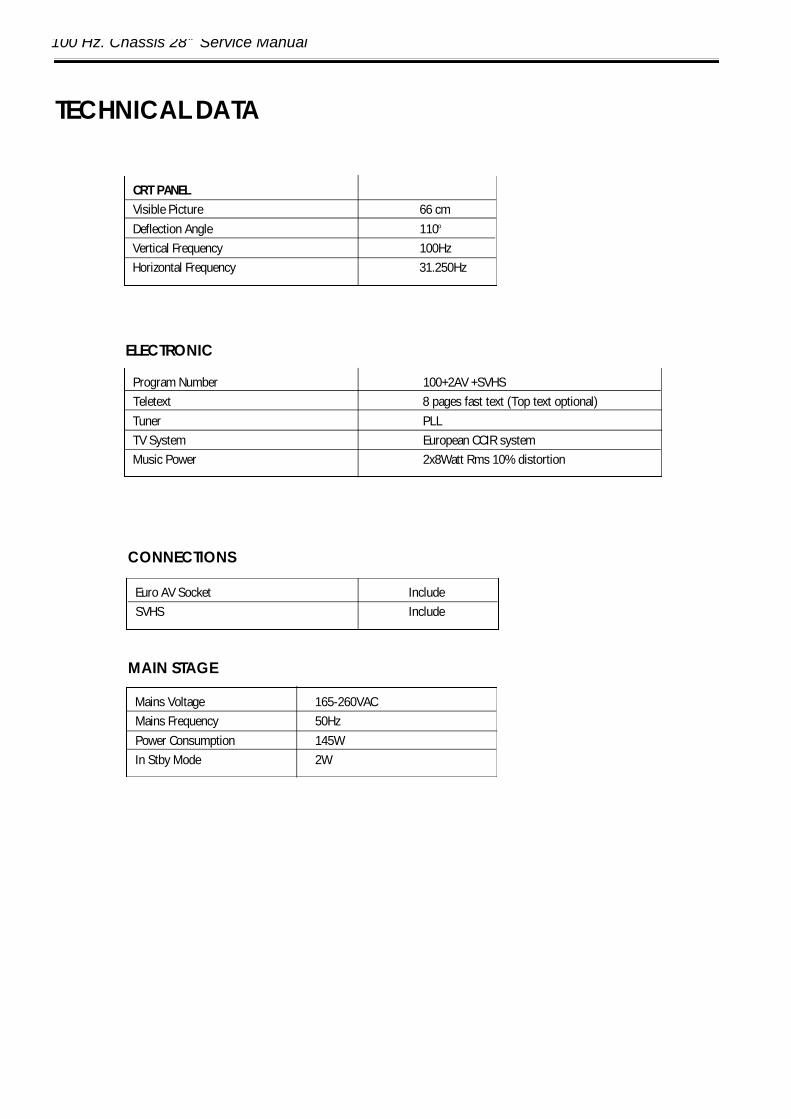
TECHNICAL DATA
ELECTRONIC
CONNECTIONS
MAIN STAGE
Mains Voltage 165-260VACMains Frequency 50HzPower Consumption 145WIn Stby Mode 2W
CRT PANELVisible Picture 66 cmDeflection Angle 110o
Vertical Frequency 100HzHorizontal Frequency 31.250Hz
Program Number 100+2AV +SVHSTeletext 8 pages fast text (Top text optional)Tuner PLLTV System European CCIR systemMusic Power 2x8Watt Rms 10% distortion
Euro AV Socket IncludeSVHS Include
100 Hz. Chassis 28” Service Manual
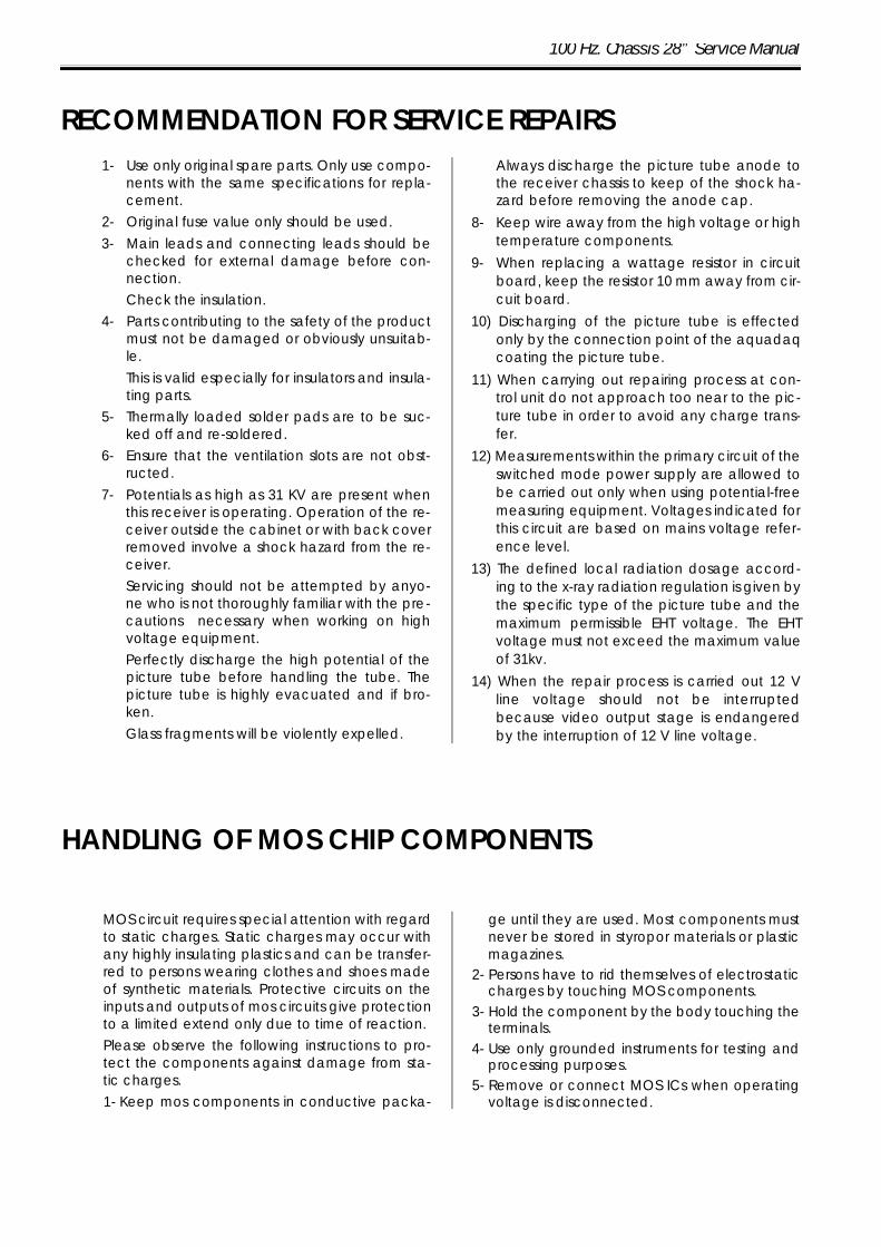
RECOMMENDATION FOR SERVICE REPAIRS1- Use only original spare parts. Only use compo-
nents with the same specifications for repla-cement.
2- Original fuse value only should be used.3- Main leads and connecting leads should be
checked for external damage before con-nection. Check the insulation.
4- Parts contributing to the safety of the productmust not be damaged or obviously unsuitab-le. This is valid especially for insulators and insula-ting parts.
5- Thermally loaded solder pads are to be suc-ked off and re-soldered.
6- Ensure that the ventilation slots are not obst-ructed.
7- Potentials as high as 31 KV are present whenthis receiver is operating. Operation of the re-ceiver outside the cabinet or with back coverremoved involve a shock hazard from the re-ceiver.Servicing should not be attempted by anyo-ne who is not thoroughly familiar with the pre-cautions necessary when working on highvoltage equipment.Perfectly discharge the high potential of thepicture tube before handling the tube. Thepicture tube is highly evacuated and if bro-ken.Glass fragments will be violently expelled.
Always discharge the picture tube anode tothe receiver chassis to keep of the shock ha-zard before removing the anode cap.
8- Keep wire away from the high voltage or hightemperature components.
9- When replacing a wattage resistor in circuitboard, keep the resistor 10 mm away from cir-cuit board.
10) Discharging of the picture tube is effectedonly by the connection point of the aquadaqcoating the picture tube.
11) When carrying out repairing process at con-trol unit do not approach too near to the pic-ture tube in order to avoid any charge trans-fer.
12) Measurements within the primary circuit of theswitched mode power supply are allowed tobe carried out only when using potential-freemeasuring equipment. Voltages indicated forthis circuit are based on mains voltage refer-ence level.
13) The defined local radiation dosage accord-ing to the x-ray radiation regulation is given bythe specific type of the picture tube and themaximum permissible EHT voltage. The EHTvoltage must not exceed the maximum valueof 31kv.
14) When the repair process is carried out 12 Vline voltage should not be interruptedbecause video output stage is endangeredby the interruption of 12 V line voltage.
HANDLING OF MOS CHIP COMPONENTS
MOS circuit requires special attention with regardto static charges. Static charges may occur withany highly insulating plastics and can be transfer-red to persons wearing clothes and shoes madeof synthetic materials. Protective circuits on theinputs and outputs of mos circuits give protectionto a limited extend only due to time of reaction.Please observe the following instructions to pro-tect the components against damage from sta-tic charges.1- Keep mos components in conductive packa-
ge until they are used. Most components mustnever be stored in styropor materials or plasticmagazines.
2- Persons have to rid themselves of electrostaticcharges by touching MOS components.
3- Hold the component by the body touching theterminals.
4- Use only grounded instruments for testing andprocessing purposes.
5- Remove or connect MOS ICs when operatingvoltage is disconnected.
100 Hz. Chassis 28” Service Manual
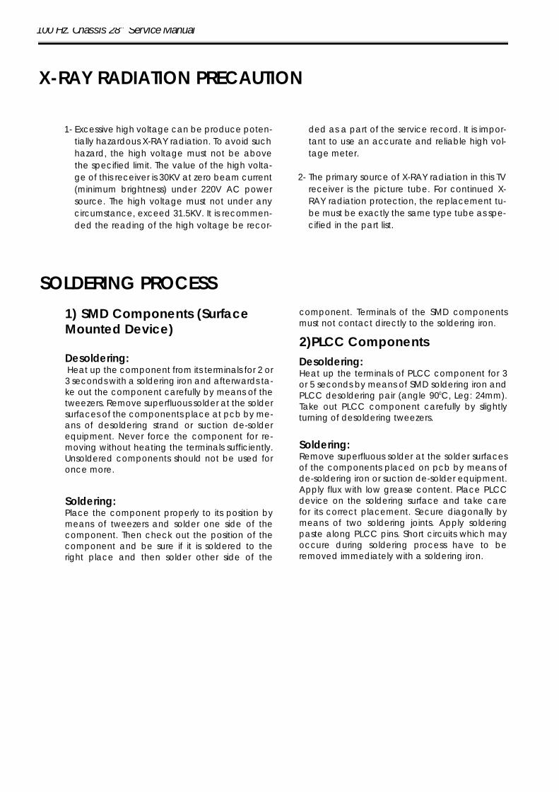
X-RAY RADIATION PRECAUTION
1- Excessive high voltage can be produce poten-tially hazardous X-RAY radiation. To avoid suchhazard, the high voltage must not be abovethe specified limit. The value of the high volta-ge of this receiver is 30KV at zero beam current(minimum brightness) under 220V AC powersource. The high voltage must not under anycircumstance, exceed 31.5KV. It is recommen-ded the reading of the high voltage be recor-
ded as a part of the service record. It is impor-tant to use an accurate and reliable high vol-tage meter.
2- The primary source of X-RAY radiation in this TVreceiver is the picture tube. For continued X-RAY radiation protection, the replacement tu-be must be exactly the same type tube as spe-cified in the part list.
SOLDERING PROCESS1) SMD Components (SurfaceMounted Device)
Desoldering:Heat up the component from its terminals for 2 or3 seconds with a soldering iron and afterwards ta-ke out the component carefully by means of thetweezers. Remove superfluous solder at the soldersurfaces of the components place at pcb by me-ans of desoldering strand or suction de-solderequipment. Never force the component for re-moving without heating the terminals sufficiently.Unsoldered components should not be used foronce more.
Soldering: Place the component properly to its position bymeans of tweezers and solder one side of thecomponent. Then check out the position of thecomponent and be sure if it is soldered to theright place and then solder other side of the
component. Terminals of the SMD componentsmust not contact directly to the soldering iron.
2)PLCC ComponentsDesoldering: Heat up the terminals of PLCC component for 3or 5 seconds by means of SMD soldering iron andPLCC desoldering pair (angle 900C, Leg: 24mm).Take out PLCC component carefully by slightlyturning of desoldering tweezers.
Soldering: Remove superfluous solder at the solder surfacesof the components placed on pcb by means ofde-soldering iron or suction de-solder equipment.Apply flux with low grease content. Place PLCCdevice on the soldering surface and take carefor its correct placement. Secure diagonally bymeans of two soldering joints. Apply solderingpaste along PLCC pins. Short circuits which mayoccure during soldering process have to beremoved immediately with a soldering iron.
100 Hz. Chassis 28” Service Manual
100 Hz. Chassis 28” Service Manual
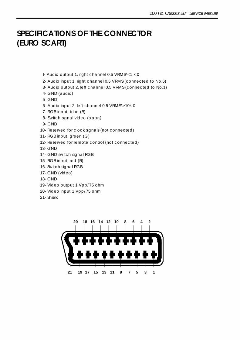
SPECIFICATIONS OF THE CONNECTOR(EURO SCART)
I- Audio output 1. right channel 0.5 VRMS/<1 k 0
2- Audio input 1. right channel 0.5 VRMS (connected to No.6)3- Audio output 2. left channel 0.5 VRMS (connected to No.1)4- GND (audio)5- GND6- Audio input 2. left channel 0.5 VRMS/>10k 07- RGB input, blue (B)8- Switch signal video (status)9- GND
10- Reserved for clock signals (not connected)11- RGB input, green (G)12- Reserved for remote control (not connected)13- GND14- GND switch signal RGB15- RGB input, red (R)16- Switch signal RGB17- GND (video)18- GND19- Video output 1 Vpp/75 ohm20- Video input 1 Vpp/75 ohm21- Shield
20 18 16 14 12 10 8 6 4 2
21 19 17 15 13 11 9 7 5 3 1
100 Hz. Chassis 28” Service Manual
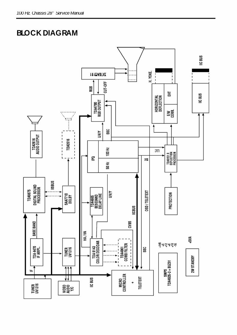
BLOCK DIAGRAM
100 Hz. Chassis 28” Service Manual
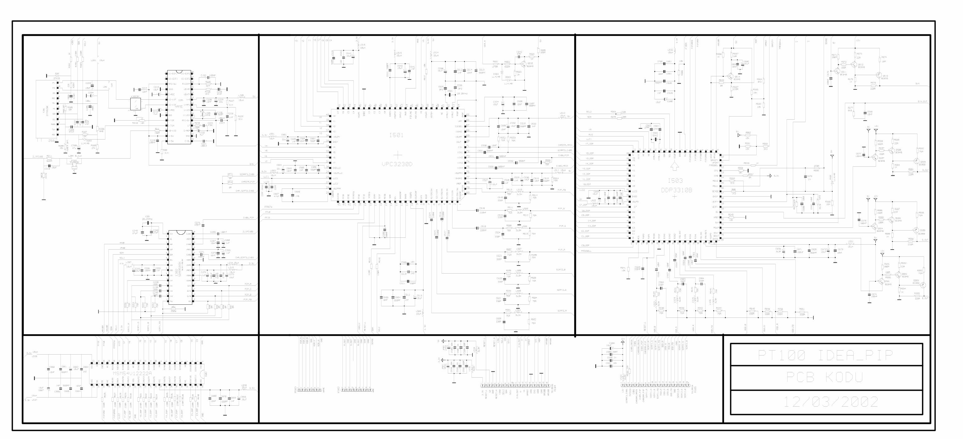
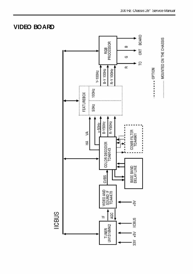
VIDEO BOARD
100 Hz. Chassis 28” Service Manual
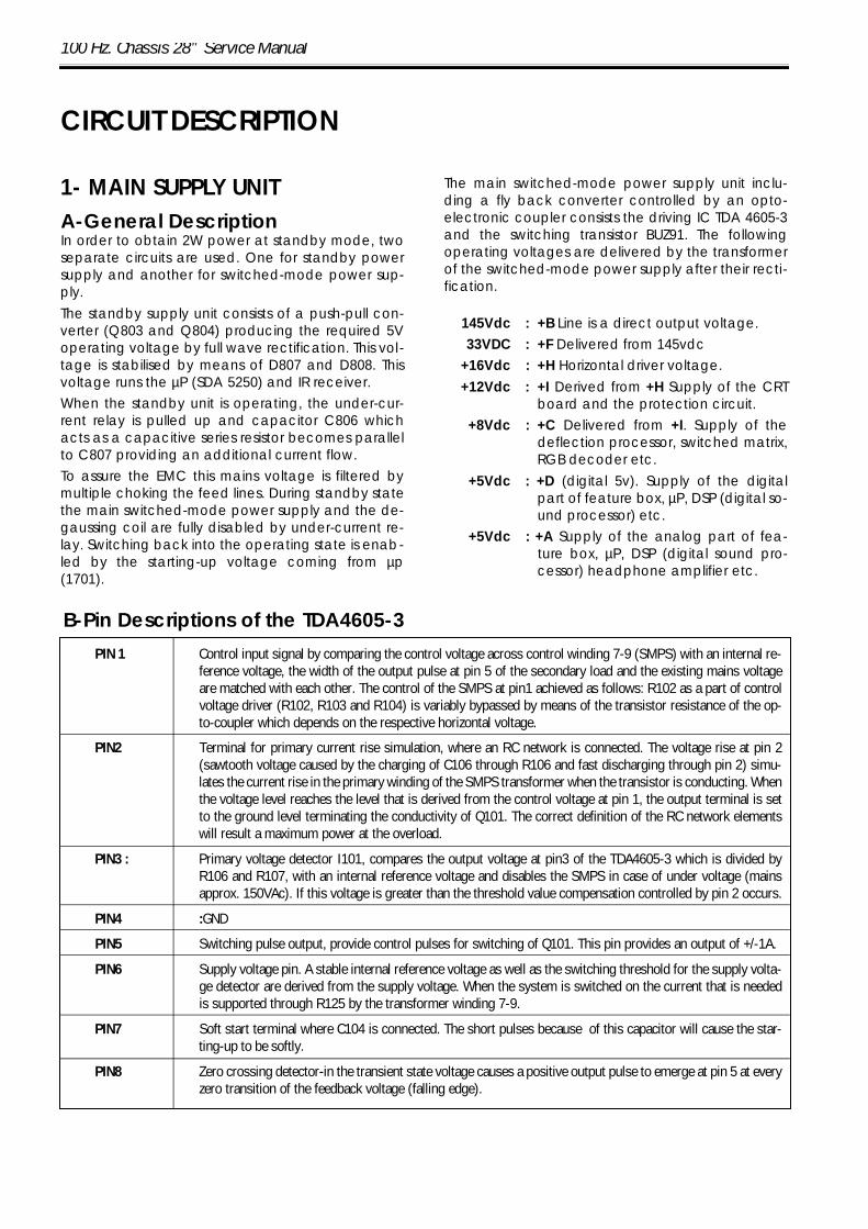
1- MAIN SUPPLY UNIT A-General DescriptionIn order to obtain 2W power at standby mode, twoseparate circuits are used. One for standby powersupply and another for switched-mode power sup-ply. The standby supply unit consists of a push-pull con-verter (Q803 and Q804) producing the required 5Voperating voltage by full wave rectification. This vol-tage is stabilised by means of D807 and D808. Thisvoltage runs the µP (SDA 5250) and IR receiver. When the standby unit is operating, the under-cur-rent relay is pulled up and capacitor C806 whichacts as a capacitive series resistor becomes parallelto C807 providing an additional current flow. To assure the EMC this mains voltage is filtered bymultiple choking the feed lines. During standby statethe main switched-mode power supply and the de-gaussing coil are fully disabled by under-current re-lay. Switching back into the operating state is enab-led by the starting-up voltage coming from µp(1701).
The main switched-mode power supply unit inclu-ding a fly back converter controlled by an opto-electronic coupler consists the driving IC TDA 4605-3and the switching transistor BUZ91. The followingoperating voltages are delivered by the transformerof the switched-mode power supply after their recti-fication.
145Vdc : +B Line is a direct output voltage. 33VDC : +F Delivered from 145vdc
+16Vdc : +H Horizontal driver voltage. +12Vdc : +I Derived from +H Supply of the CRT
board and the protection circuit. +8Vdc : +C Delivered from +I. Supply of the
deflection processor, switched matrix,RGB decoder etc.
+5Vdc : +D (digital 5v). Supply of the digitalpart of feature box, µP, DSP (digital so-und processor) etc.
+5Vdc : +A Supply of the analog part of fea-ture box, µP, DSP (digital sound pro-cessor) headphone amplifier etc.
CIRCUIT DESCRIPTION
PIN 1 Control input signal by comparing the control voltage across control winding 7-9 (SMPS) with an internal re-ference voltage, the width of the output pulse at pin 5 of the secondary load and the existing mains voltageare matched with each other. The control of the SMPS at pin1 achieved as follows: R102 as a part of controlvoltage driver (R102, R103 and R104) is variably bypassed by means of the transistor resistance of the op-to-coupler which depends on the respective horizontal voltage.
PIN2 Terminal for primary current rise simulation, where an RC network is connected. The voltage rise at pin 2(sawtooth voltage caused by the charging of C106 through R106 and fast discharging through pin 2) simu-lates the current rise in the primary winding of the SMPS transformer when the transistor is conducting. Whenthe voltage level reaches the level that is derived from the control voltage at pin 1, the output terminal is setto the ground level terminating the conductivity of Q101. The correct definition of the RC network elementswill result a maximum power at the overload.
PIN3 : Primary voltage detector I101, compares the output voltage at pin3 of the TDA4605-3 which is divided byR106 and R107, with an internal reference voltage and disables the SMPS in case of under voltage (mainsapprox. 150VAc). If this voltage is greater than the threshold value compensation controlled by pin 2 occurs.
PIN4 :GND
PIN5 Switching pulse output, provide control pulses for switching of Q101. This pin provides an output of +/-1A.
PIN6 Supply voltage pin. A stable internal reference voltage as well as the switching threshold for the supply volta-ge detector are derived from the supply voltage. When the system is switched on the current that is neededis supported through R125 by the transformer winding 7-9.
PIN7 Soft start terminal where C104 is connected. The short pulses because of this capacitor will cause the star-ting-up to be softly.
PIN8 Zero crossing detector-in the transient state voltage causes a positive output pulse to emerge at pin 5 at everyzero transition of the feedback voltage (falling edge).
B-Pin Descriptions of the TDA4605-3
100 Hz. Chassis 28” Service Manual
C-Starting Voltage After switching on the receiver with the mains but-ton, approximately 320V is present on the chargingcapacitor C109. Through the resistor R125 the supplyvoltage of I101 (pin 6) rises to 12 V. Also 5 Vstby sup-ply from the standby power the supply stage is pre-sent.
D-Power Supply The power supply for the receiver employs a free-running switched mode power supply stage with aswitching frequency of 35KHz at maximum andI90KHz at minimum load and with a maximum po-wer of 200W. For this reason, a Power Field EffectTransistor is required for the high voltage transistorQ101. The I101 is responsible for driving the MOS po-wer transistor Q101 and also for all control and mo-nitoring functions in the power supply. At Standbymode, the switched mode power supply circuit isswitched off. The power consumption is approxima-tely 2W. In this mode, only the µp stage and tuningmodule is fed with +5Vstby from the “standby” po-wer transformer.
E-Operation At pin 2 of I101, a saw tooth signal is present and thishas a lower reversal point at approx. 1,1V and anupper reversal point at 2,2V. This saw tooth signal iscompared by a comparator with the input currentat pin1. If the saw tooth signal exceeds the level atpin1, the comparator switches off the high voltagetransistor Q101. In order to switch on the transistoragain, there must be a zero-cross over signal atpin8. This pin is connected to the transformer win-
ding 2/4 to identify the zero cross-over.
F-The Control If the transformer is overloaded, all voltages reduce.For controlling the voltage drop, diode D101 is used.Like the voltages when the transformer is loaded, al-so the voltage on diode D101 decreases resulting adecreased input current of I101-(pin 1). In this casethe conduction time of the transistor Q101 incre-ases. As the operating supply for the line output stage ef-fects the line width, it is necessary for the +B voltage(operating supply for the line output stage) to bestable.Rising in +B causes the voltage of the optocouplerI102 to decrease. The LED in the optocoupler beco-mes brighter and the internal transistor between pins4 and 5 becomes less resistive. This causes the volta-ge of I101-(pin1) to increase and the conducting ti-me of the high voltage transistor compared with thesawtooth on pin 2 shorter. As a result the +B supplyreduces.
G-Overcurrent Protection The Ics (I101) internal circuit monitors the driving pul-ses of the switching transistor Q101 by means of thevoltage the sawtooth signal at pin 2 of I1O1. The sawtooth voltage on I101 -(pin2), supplies the monito-ring of the driving pulses to the switching transistorQ101. If too much current flows through the Power-MOS transistor during an over-load of the powersupply, the I101 automatically switches the powersupply off.
A-General DescriptionThe infra-red receiver decodes the infra-red bi-phasesignals for µP I701, the master processor. Also the IR-processor can switch the power supply on or off. The master processor is responsible for the control ofthe whole system of TV receiver. The set-up data andthe settings are stored in the EEPROM I703 and the sys-tem control programme is stored in the EPROM I702.The control and command functions are carried outby the 8bit microcontroller SDA5250 co-operating withthe EEPROM I703 and EPROM I702. Since the microcontroller itself does not include aROM space, the required operating system will be ob-tained by using an external EPROM I702. External EP-ROM contains the specific software program whichcorresponds to the system of the TV set.
The power supply of the microcontroller is realised bythe standby power supply unit (50mA). The low activereset pin 28 is kept as low level for at least 10ms by me-ans of trigger circuit Q701 and Q702 when the mainsvoltage is applied by switching on the TV set. 18 MHzquartz device X701 acts as a clock generator. Q708,Q709, Q710 and Q711 act as a buffer for supportingall of the IIC BUS ICs. Q704, Q705 , Q706 and Q707 arebuffer transistors for OSD.
B- Service and Special FunctionsUsing RC (Remote control) A) When the EPROM I702 is out of work and should be
changed, the service technician should order anew EPROM according to the version numberwhich is written on the IC. EPROM includes the sys-tem software (BIOS) for TV.
2- CONTROL UNIT:
100 Hz. Chassis 28” Service Manual
B) When the EEPROM I703 is out of work and shouldbe changed, the service technician should fol-low the below steps in order to supply the neces-sary adjustments. Menu including the deflectionand colour data can be loaded via remotecontroller.
Factory Set Values:This function provides the user fast programming wit-hout using the menus. This function is especially forthe production line at the factory.
Move the cursor to this line
Press OK
TV will automatically switch to the *** line. If the TV isswitched off and switch on again it will automati-cally switch from the Automatic Search Mode. Du-ring the production process at the factory setting thisfunction is the last step before the packing of the set,so the user can have the Automatic Program Searchvery quickly for the very first time. (See the related section at the User Manual)
Geometry : This function provides the service technician to ad-just the geometry parameters very quickly in anyrepair process. These parameters and their stepranges are as follows.
H-Shift : steps:0-63 H-Amplitude : steps:0-63 S-Correction : steps:0-63 V-Amplitude : steps:0-63
V-Shift : steps:0-7E/W Amplitude : steps:0-63 E/W- Shape : steps:0-63E/W- Tilt : steps:0-7
You should store these set values by moving the cur-sor to the “memorize” line.
Video: This function provides the operator at the factory orthe service technician to adjust the White Balanceparameters.
Red Gain : Red adjustment at max. Beam current
Green Gain : Green adjustment at max. Beam current
Blue Gain : Blue adjustment at max. Beam current
Red Level : Red adjustment at min. Beam current
Green Level : Green adjustment at min. Beam current
Blue Level : Blue adjustment at min. Beam current
Peak White : It is for the screen adjustment
Grid 2 Adj : This adjustment is used at the factory during the production.
You should store these set values by moving the cur-sor to the “memorize” line.
Tuner Parameters : These values are fixed valuesand should not be changed.
EHT Compensation: 17AGC Adjust :This value should be
kept as it is, unless theEEPROM is changed.Otherwise it should beadjusted until not ha-ving a snowy picture.
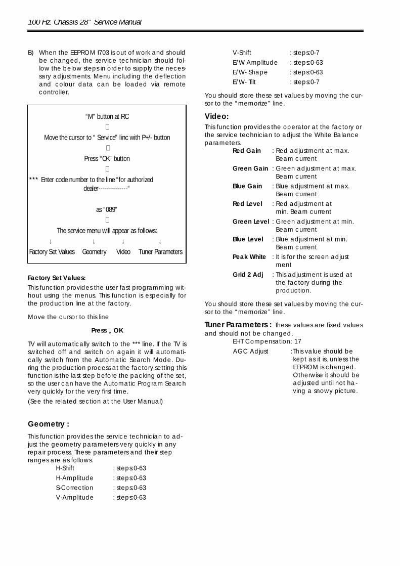
“M” button at RC ⇓
Move the cursor to “ Service” linc with P+/- button ⇓
Press “OK” button ⇓
*** Enter code number to the line “for authorized dealer--------------“
as “089”⇓
The service menu will appear as follows: ↓ ↓ ↓ ↓
Factory Set Values Geometry Video Tuner Parameters
100 Hz. Chassis 28” Service Manual
C) Feature BoxFeature Box is completely shielded as it is the most im-portant and sensitive part of 100 Hz Chassis. The YUVsignals which are for 50Hz are converted to 100Hz sig-nals by means of sampling and scanning twice ofeach sampled signal. Inside of the feature box thereare Analog-to-Digital converter, Clock Synchronisati-on Generator, Memory Synchronisation Generator,Digital-to-Analog Converter and Sequential AccessMemory. The input signals to the Feature Box are Ho-rizontal Sync, Vertical Sync, CVBS and YUV signals,SDA, SCL and LLC as well as 5V supply and ground.Analog YUV signals are converted to the digital sig-nals at ADC by means of the synchronisation pulsesfrom SDA9257 which uses analog CVBS signal for pro-viding the necessary sync pulses. The ADC conversionare processed at SDA9205. SDA9220 is responsible fordriving the SDA9254 (TV- Sequential Access Memory)and generating sync signals. Together with the otherdevices of the Feature Box it enhances picture qu-ality. SDA9254 is a combination of the TV sequentialaccess memory and an adaptive filter which is usedto enhance noisy input signals. SDA9280 is a DisplayProcessor which accepts four different data input for-mats. These are IIC, Y, B-Y, R-Y. The input data are di-gital but the output are analog. This IC is the last stepat the feature box .
3- DEFLECTION UNITThe programmable deflection processor TDA9151Bprovides the driving pulses required for driving the ho-rizontal and vertical output stages operating accor-ding to the 100Hz deflection principle. Apart from the-se, the above mentioned processor is also used forcontrolling the east-west circuit, carrying out aswitch-off function (protection circuit) and providingthe super sand castle pulse (SSC100) for the video sig-nal amplifier. This processor is controlled via an I2C BUSand receives the synchronisation pulses from the IPQ-BOX (as well as LLC-signal (line locked signal)).
PIN 1: Horizontal Flyback Input Input pin for retrace pulses having an amplitude of100Vpp by means of capacitive divider C208/C209.The retrace pulse is needed for the phase control ofthe driving pulse and the SSC pulse.
PIN 2: Display Super Sand Castle Input /Output From this terminal a double-level SC pulse is provided.The first level i.e. 2.5V is for horizontal and verticalblanking where as the second level i.e. 4,5V is usedfor video clamping. Further more at pin2 the verticaldeflection process is monitored. That means, in caseof missing vertical pulses from I202( pin8), pin2 will belocked to 2,5V and the video channel will be control-led to black level.
PIN 6: EAST-WEST GEOMETRY OUTPUT Output for east-west geometry provides the adjust-ment of horizontal deflection amplitude, picture
width, parabolic east-west correction, east-west pincushion correction and also parabolic correction oftrapezium distortions.
PIN 7: EHT COMPENSATIONEHT compensation pin is an input for keeping the pic-ture size constant although the value of EHT voltagechanges (delivered from aquadac coating of thepicture tube). ***The EHT voltage transformer provides following vol-tages: EHT voltage 30KVDc. Focusing and G2 voltage. Filament voltage for picture tube. +17Vdc+40Vdc +220Vdc. In order to be able to adjust the horizontal amplitudeof the picture (picture width) and the raster correc-tion independently from the EHT voltage, the line out-put stage is connected to a diode modulator. Onebranch of the bridge consists of C211 and C212,another one consists of deflection coil, linearity coil,C213, and the bridge coil L207. At the diagonalbranch C215 is placed where as part of the tracecapacitance it simultaneously contributes to theinternal pincushion correction. The control circuit ofthe EAST-WEST correction is connected via L204.
PIN 8: Pin8 is designed to determine the reference currentfor the complete vertical deflection current.
PIN 9:Pin 9 is for flash over protection and is not used at thischassis,
PIN 10: This pin represents the output terminal for the verticalsynchronisation. Pulse is the drive input of the differ-ential amplifier stage belonging to the vertical out-put.
PIN 11:At this IC via I2CBUS, it is possible to adjust the follow-ing values: Amplitude of vertical deflection signal 80%, tangen-tial correction from 0 to 16%, vertical shift centering in7 steps from - 1,5% to +1,5% and 16/9 change-over.
Pin 12: VA Input The vertical synchronisation input coming from theFeature Box
PIN 13: HA InputHorizontal synchronisation input coming from theFeature Box.
PIN 14: LLC Input This signal is for the line and vertical oscillator. WithoutLLC signal (27MHz) this IC can not operate.
100 Hz. Chassis 28” Service Manual
1) TDA4780
2) TDA4665
3) TDA9143
4) SAA4961
5) TDA4470
6) TDA9151
7) TDA8540
8) TDA8351
9) TDA9875-A
10) TDA2616
11) TDA4605-3
12) TDA6111Q
13) M27C2001
14) ST24C16
15) SAA7710
16) TDA7053 A
17) SDA5250
COMPONENTDESCRIPTIONS
100 Hz. Chassis 28” Service Manual
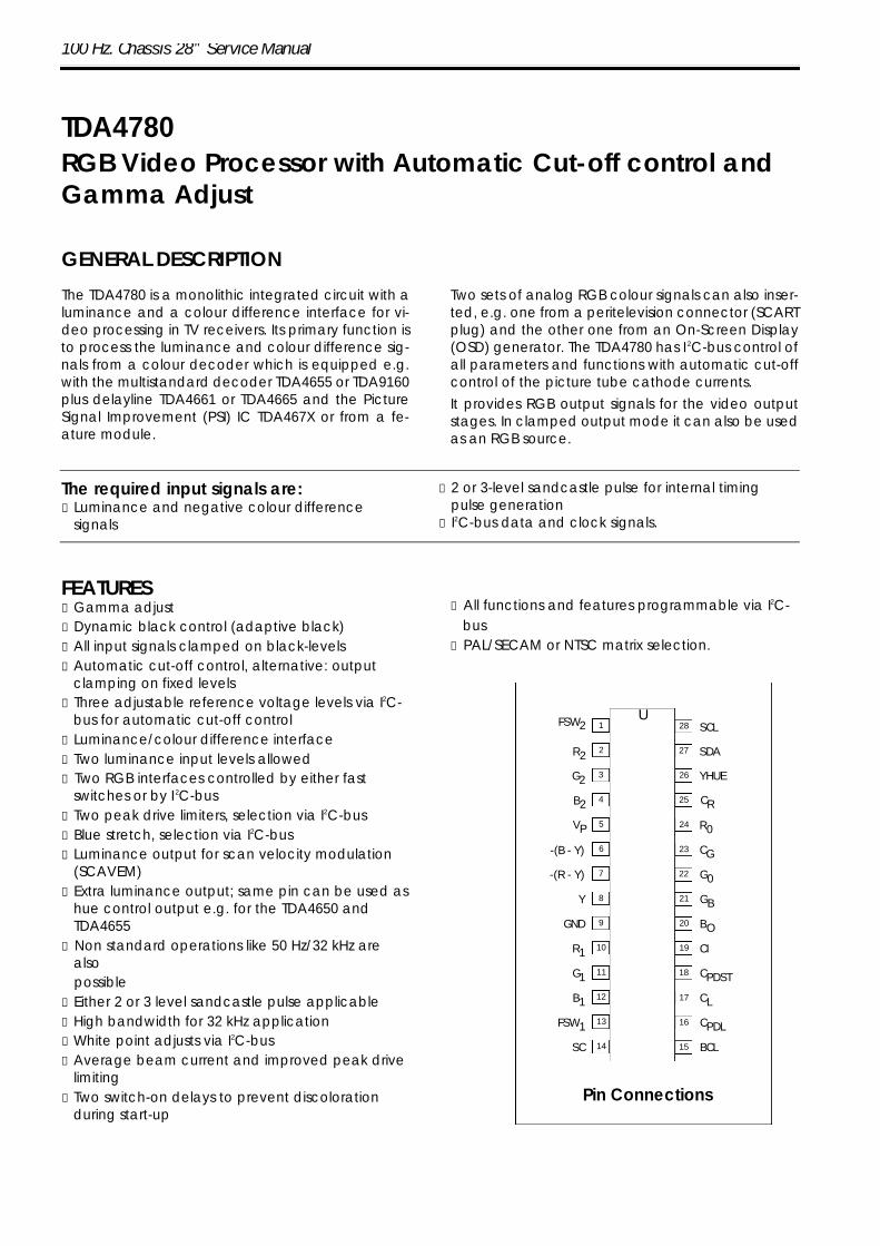
The TDA4780 is a monolithic integrated circuit with aluminance and a colour difference interface for vi-deo processing in TV receivers. Its primary function isto process the luminance and colour difference sig-nals from a colour decoder which is equipped e.g.with the multistandard decoder TDA4655 or TDA9160plus delayline TDA4661 or TDA4665 and the PictureSignal Improvement (PSI) IC TDA467X or from a fe-ature module.
Two sets of analog RGB colour signals can also inser-ted, e.g. one from a peritelevision connector (SCARTplug) and the other one from an On-Screen Display(OSD) generator. The TDA4780 has I 2C-bus control ofall parameters and functions with automatic cut-offcontrol of the picture tube cathode currents. It provides RGB output signals for the video outputstages. In clamped output mode it can also be usedas an RGB source.
FEATURESu Gamma adjustu Dynamic black control (adaptive black)u All input signals clamped on black-levelsu Automatic cut-off control, alternative: output
clamping on fixed levelsu Three adjustable reference voltage levels via I2C-
bus for automatic cut-off controlu Luminance/colour difference interfaceu Two luminance input levels allowedu Two RGB interfaces controlled by either fast
switches or by I2C-busu Two peak drive limiters, selection via I2C-busu Blue stretch, selection via I2C-busu Luminance output for scan velocity modulation
(SCAVEM)u Extra luminance output; same pin can be used as
hue control output e.g. for the TDA4650 andTDA4655
u Non standard operations like 50 Hz/32 kHz arealsopossible
u Either 2 or 3 level sandcastle pulse applicableu High bandwidth for 32 kHz applicationu White point adjusts via I2C-busu Average beam current and improved peak drive
limitingu Two switch-on delays to prevent discoloration
during start-up
u All functions and features programmable via I2C-bus
u PAL/SECAM or NTSC matrix selection.
1
2
3
4
5
6
7
28
27
26
25
24
23
22
FSW2
R2
G2
B2
VP
-(B - Y)
-(R - Y)
U
Pin Connections
SCL
SDA
YHUE
CR
R0
CG
G0
8 21Y GB
9 20GND BO
10 19R1 CI
11 18G1 CPDST
12 17B1 CL
13 16FSW1 CPDL
14 15SC BCL
GENERAL DESCRIPTION
TDA4780RGB Video Processor with Automatic Cut-off control andGamma Adjust
The required input signals are:u Luminance and negative colour difference
signals
u 2 or 3-level sandcastle pulse for internal timingpulse generation
u I2C-bus data and clock signals.
100 Hz. Chassis 28” Service Manual
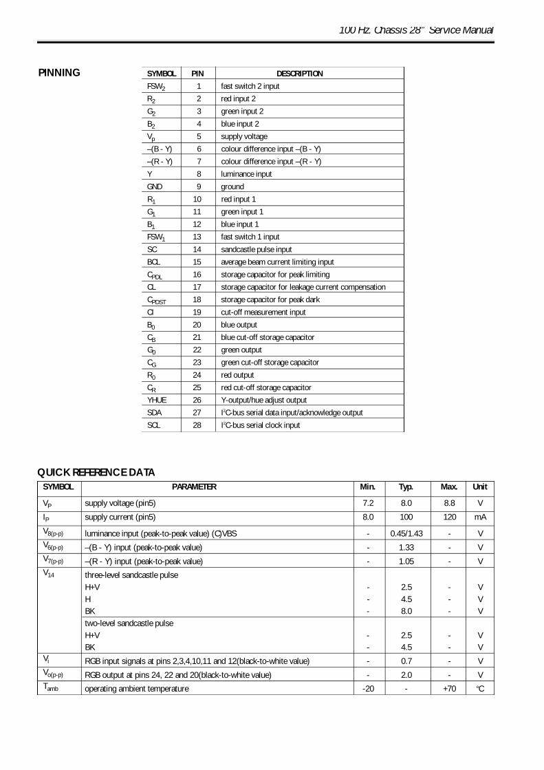
SYMBOL PIN DESCRIPTION
FSW2 1 fast switch 2 input
R2 2 red input 2
G2 3 green input 2
B2 4 blue input 2
Vp 5 supply voltage
–(B - Y) 6 colour difference input –(B - Y)
–(R - Y) 7 colour difference input –(R - Y)
Y 8 luminance input
GND 9 ground
R1 10 red input 1
G1 11 green input 1
B1 12 blue input 1
FSW1 13 fast switch 1 input
SC 14 sandcastle pulse input
BCL 15 average beam current limiting input
CPDL 16 storage capacitor for peak limiting
CL 17 storage capacitor for leakage current compensation
CPDST 18 storage capacitor for peak dark
CI 19 cut-off measurement input
B0 20 blue output
CB 21 blue cut-off storage capacitor
G0 22 green output
CG 23 green cut-off storage capacitor
R0 24 red output
CR 25 red cut-off storage capacitor
YHUE 26 Y-output/hue adjust output
SDA 27 I2C-bus serial data input/acknowledge output
SCL 28 I2C-bus serial clock input
QUICK REFERENCE DATA
PINNING
SYMBOL PARAMETER Min. Typ. Max. Unit
VP supply voltage (pin5) 7.2 8.0 8.8 V
IP supply current (pin5) 8.0 100 120 mA
V8(p-p) luminance input (peak-to-peak value) (C)VBS - 0.45/1.43 - VV6(p-p) –(B - Y) input (peak-to-peak value) - 1.33 - VV7(p-p) –(R - Y) input (peak-to-peak value) - 1.05 - VV14 three-level sandcastle pulse
H+V - 2.5 - VH - 4.5 - VBK - 8.0 - Vtwo-level sandcastle pulseH+V - 2.5 - VBK - 4.5 - V
Vi RGB input signals at pins 2,3,4,10,11 and 12(black-to-white value) - 0.7 - VVo(p-p) RGB output at pins 24, 22 and 20(black-to-white value) - 2.0 - VTamb operating ambient temperature -20 - +70 oC
100 Hz. Chassis 28” Service Manual
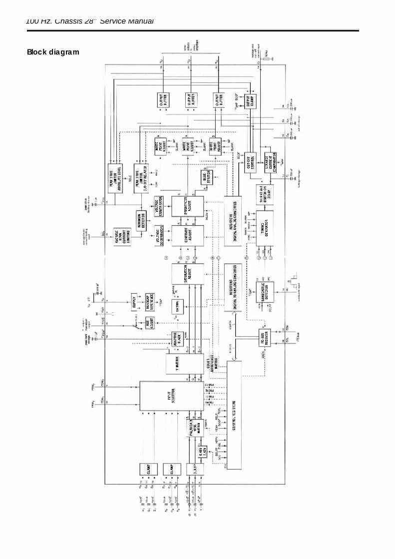
Block diagram
100 Hz. Chassis 28” Service Manual
Signal input stagesThe TDA4780 contains 3 sets of input signalstages for:
1.Luminance/colour-difference signals:a) Y: 0.45 V (p-p) VBS or 1.43 V (p-p)
VBS, selectable via I2C-bus.b) -(R - Y): 1.05 V (p-p).c) -(B - Y): 1.33 V (p-p).The capacitively coupled signals are matrixed to RGB signals by either a PAL/SECAM or NTSC matrix (selected via I2C-bus).
2.(RGB)1 signals (0.7 V (p-p) VB), capacitively coupled (e.g. from external source).
3.(RGB)2 signals (0.7 V (p-p) VB), capacitively coupled (e.g. videotext, OSD).
All input signals are clamped in order to havethe same black levels at the signal switch in-put. Displayed signals must be synchronouswith the sandcastle pulse.
Signal switchesBoth fast signal switches can be operated byswitching pins (e.g. SCART facilities) or set viathe I2C-bus. With the pin FSW1 the Y-CD signalsor the (RGB)1 signals can be selected, with pinFSW2 the above selected signals or the (RGB)2signals are enabled. During the vertical andhorizontal blanking time an artificial black le-vel equal to the clamped black level is inser-ted in order to clip off the sync pulse of the lu-minance signal and to suppress hum duringthe cut-off measurement time and eliminatenoise during these intervals.
Saturation, contrast and brightness adjustSaturation, contrast and brightness adjusts arecontrolled via the I2C-bus and act on Y, CD aswell as on RGB input signals. Gamma acts onthe luminance content of the input signals.
Gamma adjustThe gamma adjust stage has a non-lineartransmission characteristic according to theformula y = xgamma, where x represents the inputand y the output signal. If gamma is smallerthan unity, the lower parts of the signal areamplified with higher gain.
Automatic cut-off controlDuring leakage measurement time the leaka-ge current is compensated in order to get areference voltage at the cut-off measure-
ment info pin. This compensation value is sto-red in an external capacitor. During cut-offcurrent measurement times for the R, G and Bchannels, the voltage at this pin is comparedwith the reference voltage, which is individu-ally adjustable via I2C-bus for each colourchannel. The control voltages that are derivedin this way are stored in the external feedbackcapacitors. Shift stages add these voltages tothe corresponding output signals. The auto-matic cut-off control may be disabled via theI2C-bus. In this mode the output voltage isclamped to 2.5 V. Clamping periods are thesame as the cut-off measurement periods.
Adaptive black (ADBL)The adaptive black stage detects the lowestvoltage of the luminance component of theinternal RGB signals during the scanning timeand shifts it to the nominal black level. In orderto keep the nominal white level the contrast isincreased simultaneously.
Blue stretch (BLST)The blue stretch channel gets additional amp-lification if the blue signal is greater than 80%of the nominal signal amplitude. In the eventthe white point is shifted towards higher colo-ur temperature so that white parts of a pictu-re seem to be brighter.
Measurement pulse and blanking stageDuring the vertical and horizontal blanking ti-me and the measurement period the signalsare blanked to an ultra black level, so the le-akage current of the picture tube can be me-asured and automatically compensated for.During the cut-off measurement lines (one lineperiod for each R, G or B) the output signal le-vels are at cut-off measurement level.The vertical blanking period is timed by thesandcastle pulse. The measurement pulses (le-akage, R, G and B) are triggered by the nega-tive going edge of the vertical pulse of thesandcastle pulse and start after the followinghorizontal pulse.The IC is prepared for 2fH (32 kHz) application.
Output amplifier and white adjust potentiometer
The RGB signals are amplified to nominal 2 V(p-p), the DC-levels are shifted according tocut-off control.
FUNCTIONAL DESCRIPTION
100 Hz. Chassis 28” Service Manual
The nominal signal amplitude can be variedby ±50% by the white point adjustment via theI2C-bus (individually for RGB respect).
Signal limitingThe TDA4780 provides two kinds of signal limi-ting.First, an average beam limiting, that reducessignal level if a certain average is exceeded.Second, a peak drive limiting, that is activatedif one of the RGB signals even shortly exceedsa via I2C-bus adjusted threshold. The latter canbe either referred to the cut-off measurementlevel of the outputs or to ground.When signal limiting occurs, contrast is redu-ced, and at minimum contrast brightness is re-duced additionally.
Sandcastle decoder and timerA 3-level detector separates the sandcastlepulse into combined line and field pulses, linepulses, and clamping pulses. The timer conta-ins a line counter and controls the cut-offcontrol measurement.Application with a 2-level 5 V sandcastle pulseis possible.
Switch on delay circuitAfter switch on all signals are blanked and awarm up test pulse is fed to the outputs duringthe cut-off measurement lines. If the voltage
at the cut-off measurement input exceeds aninternal level the cut-off control is enabled butthe signal remains still blanked. In the event ofoutput clamping, the cut-off control is disab-led and the switch on procedure will be skip-ped.
Y output and hue adjustThe TDA4780 contains a D/A converter for hueadjust. The analog information can be fed,e.g. to the multistandard decoder TDA4650 orTDA4655. This output pin may be switched to aY output signal, which can be used for scanvelocity modulation (SCAVEM). The Y output isthe Y input signal or the matrixed (RGB) inputsignal according to the switch position of thefast switch.
I2C-busThe TDA4780 contains an I2C-bus receiver forcontrol function.
ESD protectionThe Pins are provided with protection diodesagainst ground and supply voltage (seeChapter "internal pin configurations"). I2C-businput pins do not shunt the I2C-bus signals inthe event of missing supply voltage.
EMCThe pins are protected against electromag-netic radiation.
100 Hz. Chassis 28” Service Manual
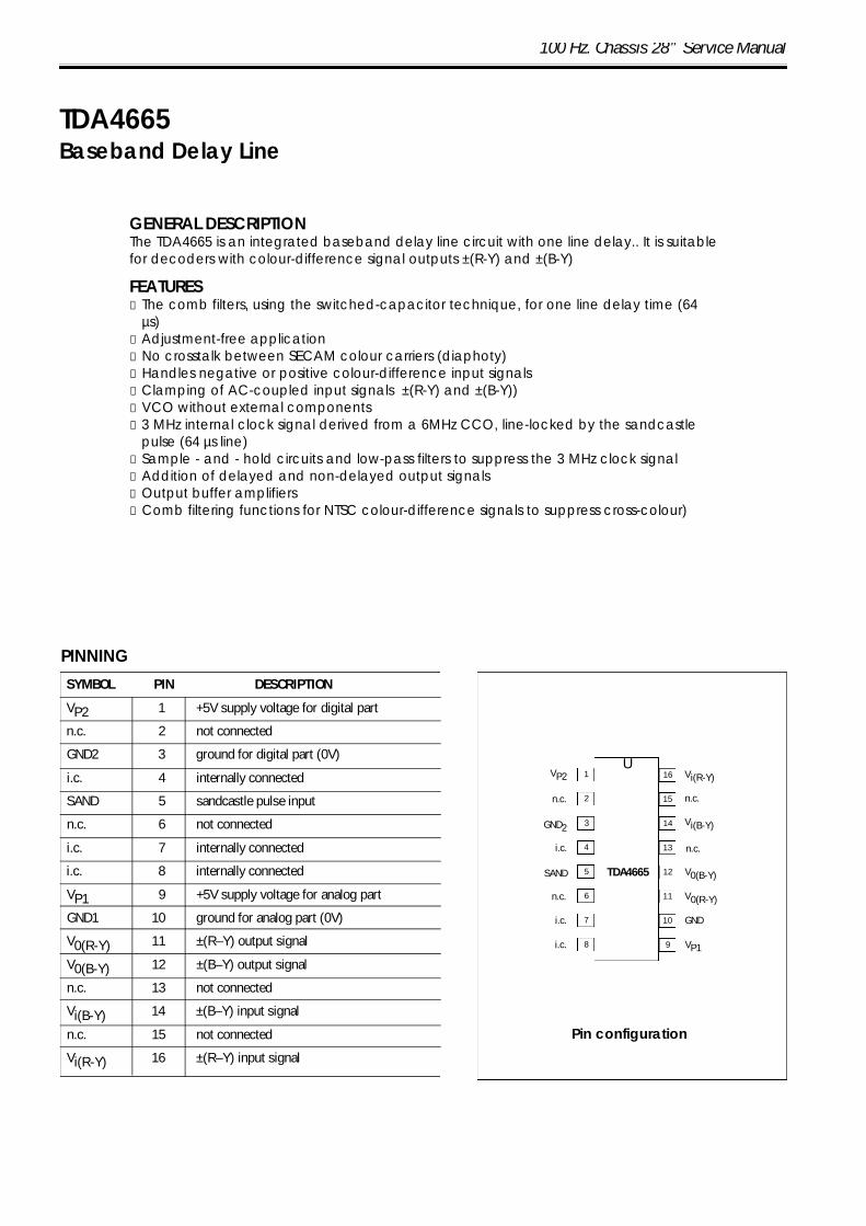
TDA4665Baseband Delay Line
SYMBOL PIN DESCRIPTION
VP2 1 +5V supply voltage for digital part
n.c. 2 not connected
GND2 3 ground for digital part (0V)
i.c. 4 internally connected
SAND 5 sandcastle pulse input
n.c. 6 not connected
i.c. 7 internally connected
i.c. 8 internally connected
VP1 9 +5V supply voltage for analog part
GND1 10 ground for analog part (0V)
V0(R-Y) 11 ±(R–Y) output signal
V0(B-Y) 12 ±(B–Y) output signal
n.c. 13 not connected
Vi(B-Y) 14 ±(B–Y) input signal
n.c. 15 not connected
Vi(R-Y) 16 ±(R–Y) input signal
GENERAL DESCRIPTIONThe TDA4665 is an integrated baseband delay line circuit with one line delay.. It is suitablefor decoders with colour-difference signal outputs ±(R-Y) and ±(B-Y)
FEATURESu The comb filters, using the switched-capacitor technique, for one line delay time (64
µs)u Adjustment-free applicationu No crosstalk between SECAM colour carriers (diaphoty)u Handles negative or positive colour-difference input signalsu Clamping of AC-coupled input signals ±(R-Y) and ±(B-Y))u VCO without external componentsu 3 MHz internal clock signal derived from a 6MHz CCO, line-locked by the sandcastle
pulse (64 µs line)u Sample - and - hold circuits and low-pass filters to suppress the 3 MHz clock signalu Addition of delayed and non-delayed output signalsu Output buffer amplifiersu Comb filtering functions for NTSC colour-difference signals to suppress cross-colour)
PINNING
1
2
3
4
5
6
7
8
16
15
14
13
12
11
10
9
Vi(R-Y)
n.c.
Vi(B-Y)
n.c.
V0(B-Y)
V0(R-Y)
GND
VP1
VP2
n.c.
GND2
i.c.
SAND
n.c.
i.c.
i.c.
TDA4665
Pin configuration
U
100 Hz. Chassis 28” Service Manual
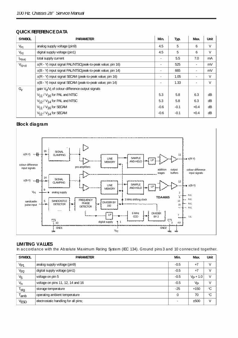
Block diagram
QUICK REFERENCE DATASYMBOL PARAMETER Min. Typ. Max. Unit
VP1 analog supply voltage (pin9) 4.5 5 6 V
VP2 digital supply voltage (pin1) 4.5 5 6 V
IP(tot) total supply current - 5.5 7.0 mA
Vi(p-p) ±(R - Y) input signal PAL/NTSC(peak-to-peak value; pin 16) - 525 - mV
±(B - Y) input signal PAL/NTSC(peak-to-peak value; pin 14) - 665 - mV
±(R - Y) input signal SECAM (peak-to-peak value; pin 16) - 1.05 - V
±(B - Y) input signal SECAM (peak-to-peak value; pin 14) - 1.33 - V
Gv gain Vo/Vi of colour-difference output signals
V11 / V16 for PAL and NTSC 5.3 5.8 6.3 dB
V12 / V14 for PAL and NTSC 5.3 5.8 6.3 dB
V11 / V16 for SECAM -0.6 -0.1 +0.4 dB
V12 / V14 for SECAM -0.6 -0.1 +0.4 dB
LIMITING VALUESIn accordance with the Absolute Maximum Rating System (IEC 134). Ground pins 3 and 10 connected together.
SYMBOL PARAMETER Min. Max. Unit
VP1 analog supply voltage (pin9) -0.5 +7 V
VP2 digital supply voltage (pin1) -0.5 +7 V
V5 voltage on pin 5 -0.5 VP + 1.0 V
Vn voltage on pins 11, 12, 14 and 16 -0.5 VP V
Tstg storage temperature -25 +150 oC
Tamb operating ambient temperature 0 70 oC
VESD electrostatic handling for all pins; - ±500 V
±(R-Y)16
colour-differenceinput signals
SIGNALCLAMPING
±(B-Y)14
9
5
VP1
sandcastlepulse input
SANDCASTLEDETECTOR
SIGNALCLAMPING
FREQUENCYPHASE
DETECTORDIVIDER BY
192
LP 6 MHzCCO
DIVIDERBY 2
LP
GND1
10 digital supply
3 MHz shifting clock
1
VP2GND2
i.c.
n.c.n.c.
n.c.n.c.
±(R-Y)
colour-differenceinput signals
±(B-Y)
SAMPLEAND-HOLD LP
11
12
6
13
15
2
7
4,83
TDA4665
addition outputstages buffers
LINEMEMORY
pre-amplifiers
LINEMEMORY
SAMPLEAND-HOLD
analog supply
100 Hz. Chassis 28” Service Manual
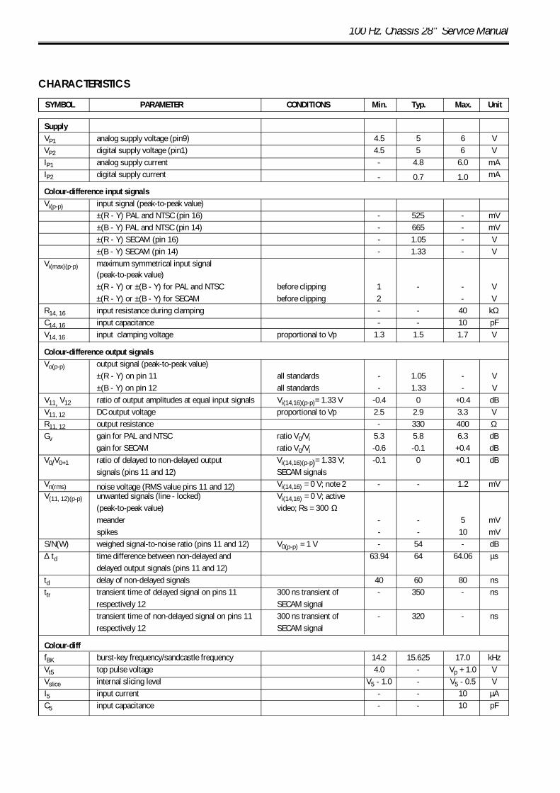
CHARACTERISTICS
SupplyVP1 analog supply voltage (pin9) 4.5 5 6 VVP2 digital supply voltage (pin1) 4.5 5 6 VIP1 analog supply current - 4.8 6.0 mAIP2 digital supply current - 0.7 1.0 mA
Colour-difference input signalsVi(p-p) input signal (peak-to-peak value)
±(R - Y) PAL and NTSC (pin 16) - 525 - mV±(B - Y) PAL and NTSC (pin 14) - 665 - mV±(R - Y) SECAM (pin 16) - 1.05 - V±(B - Y) SECAM (pin 14) - 1.33 - V
Vi(max)(p-p) maximum symmetrical input signal (peak-to-peak value)±(R - Y) or ±(B - Y) for PAL and NTSC before clipping 1 - - V±(R - Y) or ±(B - Y) for SECAM before clipping 2 - V
R14, 16 input resistance during clamping - - 40 kΩC14, 16 input capacitance - - 10 pFV14, 16 input clamping voltage proportional to Vp 1.3 1.5 1.7 V
Colour-difference output signalsVo(p-p) output signal (peak-to-peak value)
±(R - Y) on pin 11 all standards - 1.05 - V±(B - Y) on pin 12 all standards - 1.33 - V
V11, V12 ratio of output amplitudes at equal input signals Vi(14,16)(p-p)= 1.33 V -0.4 0 +0.4 dBV11, 12 DC output voltage proportional to Vp 2.5 2.9 3.3 VR11, 12 output resistance - 330 400 ΩGv gain for PAL and NTSC ratio V0/Vi 5.3 5.8 6.3 dB
gain for SECAM ratio V0/Vi -0.6 -0.1 +0.4 dBV0/V0+1 ratio of delayed to non-delayed output Vi(14,16)(p-p)= 1.33 V; -0.1 0 +0.1 dB
signals (pins 11 and 12) SECAM signalsVn(rms) noise voltage (RMS value pins 11 and 12) Vi(14,16) = 0 V; note 2 - - 1.2 mVV(11, 12)(p-p) unwanted signals (line - locked) Vi(14,16) = 0 V; active
(peak-to-peak value) video; Rs = 300 Ωmeander - - 5 mVspikes - - 10 mV
S/N(W) weighed signal-to-noise ratio (pins 11 and 12) V0(p-p) = 1 V - 54 - dB∆ td time difference between non-delayed and 63.94 64 64.06 µs
delayed output signals (pins 11 and 12)td delay of non-delayed signals 40 60 80 nsttr transient time of delayed signal on pins 11 300 ns transient of - 350 - ns
respectively 12 SECAM signaltransient time of non-delayed signal on pins 11 300 ns transient of - 320 - nsrespectively 12 SECAM signal
Colour-difffBK burst-key frequency/sandcastle frequency 14.2 15.625 17.0 kHzVt5 top pulse voltage 4.0 - Vp + 1.0 VVslice internal slicing level V5 - 1.0 - V5 - 0.5 VI5 input current - - 10 µAC5 input capacitance - - 10 pF
SYMBOL PARAMETER CONDITIONS Min. Typ. Max. Unit
100 Hz. Chassis 28” Service Manual
TDA9143I2C-BUS controlled, alignment-free PAL/NTSC/SECAM Decoder / SyncProcessor
u Multi-standard colour decoder and sync proces-sor for PAL, NTSC and SECAM
u PALplus helper blanking and EDTV-2 blankingu I2C-bus controlledu I2C-bus addresses hardware selectableu Pin compatible with TDA9141u Alignment freeu Few external componentsu Designed for use with baseband delay linesu Integrated video filtersu Adjustable luminance delayu Noise detector with I2C-bus read-outu Norm/no norm detector with I2C-bus read-outu CVBS or Y/C input, with automatic detection pos-
sibilityu CVBS output, provided I2C-bus address 8A is usedu Vertical divider systemu Two-level sandcastle signalu VA synchronization pulse (3-state)u HA synchronization pulse or clamping pulse CLP
input/outputu Line-locked clock output (6.75 MHz or 6.875 MHz)
or stand-alone I2C-bus output portu Stand-alone I2C-bus input/output port
u Colour matrix and fast YUV switchu Comb filter enable input/output with subcarrier
frequencyu Internal bypass mode of external delay line for
NTSC applicationsu Low power standby mode with 3-state YUV out-
putsu Fast blanking detector with I2C-bus read-outu Blanked or unblanked sync on Yout by I2C-bus bit
BSYu Internal MACROVISION gating for the horizontal
PLL enabled by bus bit EMG.
The TDA9143 is an 12C-bus controlled, alignment-freePAL/NTSC/SECAM decoder/sync processor withblanking facilities for PALplus and EDTV-2 signals. TheTDA9143 has been designed for use with basebandchrominance delay lines, and has a combined sub-carrier frequency/comb filter enable signal for com-munication with a PAL/NTSC comb filter.The IC can process both CVBS input signals and Y/Cinput signals. The input signal is available on an out-put pin, in the event of a Y/C signal, it is added intoa CVBS signal.The sync processor provides a two-level sandcastle,a horizontal pulse (CLP or HA pulse, bus selectable)and a vertical (VA) pulse. When the HA pulse is se-lected, a line-locked clock (LLC) signal is availableat the output port pin (6.75 MHz or 6.875 MHz).A fast switch can select either the internal Y signal
with the UV input signals, or YUV signals made of theRGB input signals. The RGB input signals can beclamped with either the internal or an externalclamping signal.Two pins with an input/output port and an outputport of the I2C-bus are available.The I2C-bus address of the TDA9143 is hardwareprogrammable.
FEATURES
GENERAL DESCRIPTION
100 Hz. Chassis 28” Service Manual
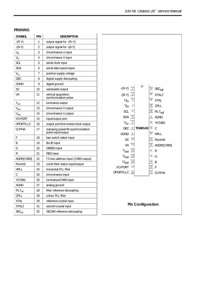
SYMBOL PIN DESCRIPTION
-(R-Y) 1 output signal for -(R–Y)
-(B-Y) 2 output signal for -(B-Y)
Uin 3 chrominance U input
Vin 4 chrominance V input
SCL 5 serial clock input
SDA 6 serial data input/output
Vcc 7 positive supply voltage
DEC 8 digital supply decoupling
DGND 9 digital ground
SC 10 sandcastle output
VA 11 vertical acquisitionsynchronization pulse
Yout 12 luminance output
Vout 13 chrominance V output
Uout 14 chrominance U output
I/O PORT 15 input/output port
OPORT/LLC 16 output port/line-locked clock output
CLP/HA 17 clamping pulse/HA synchronizationpulse input/output
F 18 fast switch select input
B 19 BLUE input
G 20 GREEN input
R 21 RED input
ADDR(CVBS) 22 I2C-bus address input (CVBS output)
Fscomb 23 comb filter status input/output
HPLL 24 horizontal PLL filter
C 25 chrominance input
Y/CVBS 26 luminance/CVBS input
AGND 27 analog ground
FILTref 28 filter reference decoupling
CPLL 29 colour PLL filter
XTAL 30 reference crystal input
XTAL2 31 second crystal input
SECref 32 SECAM reference decoupling
PINNING
1
2
3
4
5
6
7
32
31
30
29
28
27
26
-(R-Y)
-(B-Y)
UinVin
SCL
SDA
Vcc
U
Pin Configuration
SECrefXTAL2
XTAL
CPLL
FILTrefAGND
Y/CVBS8 25DEC C9 24DGND HPLL10 23SC Fscomb11 22VA ADDR(CVBS)12 21Yout R13 20Vout G14
15
16
19
18
17
UoutI/O PORT
OPORT/LLC
B
F
CLP/HA
TDA9143
The TDA9143 is an I2C-bus controlled, alignment-freePAL/NTSC/SECAM colour decoder/sync processorwhich has been designed for use with basebandchrominance delay lines. For PALplus and EDTV-2 (60Hz) signals blanking facilities are included. In the standard operating mode the I2C-bus addressis 8A. If the address input is connected to the positivesupply rail the address will change to 8E.
Input switch
The TDA9143 has a two pin input for CVBS or Y/C sig-nals which can be selected via the I2C-bus. The inputselector also has a position in which it automaticallydetects whether a CVBS or Y/C signal is on the input.In this input selector position, standard identificationfirst takes place on an added Y/CVBS and C input sig-nal.After that, both chrominance signal input amplitudesare checked once and the input with the strongestchrominance burst signal is selected. The input switchstatus is read out by the I2C-bus via output bit YC. Theauto input detector indicates YC = 1 for a VBS inputsignal (no chrominance component).
CVBS output In the standard operating mode with I2C-bus address8A, a CVBS output signal is available on the addresspin, which represents either the CVBS input signal orthe Y/C input signal, added into a CVBS signal.
RGB colour matrix
The TDA9143 has a colour matrix to convert RGB inputsignals into YUV signals. A fast switch, controlled by thesignal on pin F and enabled by I2C-bus via EFS (enab-le fast switch), can select between these YUV signalsand the YUV signals of the decoder. Mode FRGB = 1(forced RGB) overrules EFS and switches the matrixedRGB inputs to the YUV outputs.The Y signal is internally connected to the switch. The-(R-Y) and -(B-Y) output signals of the decoder first ha-ve to be delayed in external baseband chrominancedelay lines. The outputs of the delay lines must be con-nected to the UV input pins. If the RGB signals are notsynchronous with the selected decoder input signal,clamping of the RGB input signals is possible by I2C-busselection of ECL (external RGB clamp mode) and byfeeding an external clamping signal to the CLP pin.Also in external RGB clamp mode the VA output will
100 Hz. Chassis 28” Service Manual
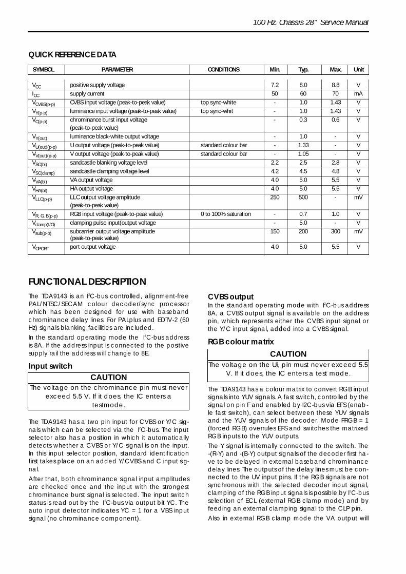
QUICK REFERENCE DATA
VCC positive supply voltage 7.2 8.0 8.8 VICC supply current 50 60 70 mAVCVBS(p-p) CVBS input voltage (peak-to-peak value) top sync-white - 1.0 1.43 VVY(p-p) luminance input voltage (peak-to-peak value) top sync-whit - 1.0 1.43 VVC(p-p) chrominance burst input voltage - 0.3 0.6 V
(peak-to-peak value)VY(out) luminance black-white output voltage - 1.0 - VVU(out)(p-p) U output voltage (peak-to-peak value) standard colour bar - 1.33 - VVV(out)(p-p) V output voltage (peak-to-peak value) standard colour bar - 1.05 - VVSC(bl) sandcastle blanking voltage level 2.2 2.5 2.8 VVSC(clamp) sandcastle clamping voltage level 4.2 4.5 4.8 VVVA(bl) VA output voltage 4.0 5.0 5.5 VVHA(bl) HA output voltage 4.0 5.0 5.5 VVLLC(p-p) LLC output voltage amplitude 250 500 - mV
(peak-to-peak value)VR, G, B(p-p) RGB input voltage (peak-to-peak value) 0 to 100% saturation - 0.7 1.0 VVclamp(I/O) clamping pulse input(output voltage - 5.0 - VVsub(p-p) subcarrier output voltage amplitude 150 200 300 mV
(peak-to-peak value)VOPORT port output voltage 4.0 5.0 5.5 V
SYMBOL PARAMETER CONDITIONS Min. Typ. Max. Unit
FUNCTIONAL DESCRIPTION
CAUTIONThe voltage on the chrominance pin must never
exceed 5.5 V. If it does, the IC enters a testmode.
CAUTIONThe voltage on the Ui, pin must never exceed 5.5
V. If it does, the IC enters a test mode.
100 Hz. Chassis 28” Service Manual
be in a high impedance OFF-state. The YUV outputscan be put in 3-state mode by bus bit LPS (low powerstandby mode).
Standard identificationThe standards which the TDA9143 can decode de-pend upon the choice of external crystals. If a 4.4 MHzand a 3.6 MHz crystal are used then SECAM, PAL4.4/3.6 and NTSC 4.4/3.6 can be decoded. If two 3.6MHz crystals are used then only PAL 3.6 and NTSC 3.6can be decoded.Which 3.6 MHz standards can be decoded dependsupon the exact frequencies of the 3.6 MHz crystals. Inan application where not all standards are requiredonly one crystal is sufficient; in this instance the crystalmust be connected to the reference crystal input (pin30). If a 4.4 MHz crystal is used it must always be con-nected to the reference crystal input. Both crystals areused to provide a reference for the filters and the ho-rizontal PLL, however, only the reference crystal is usedto provide a reference for the SECAM demodulator.To enable the calibrating circuits to be adjustedexactly, two bits from I2C-bus subaddress 00 are usedto indicate which crystals are connected to the IC.The standard identification circuit is a digital circuitwithout external components.The decoder (via the I2C-bus) can be forced to deco-de either SECAM or PAL/NTSC (but not PAL or NTSC).Crystal selection can also be forced. Information con-cerning standard and which crystal is selected andwhether the colour killer is ON or OFF is provided bythe read out.Using the forced-mode does not affect the search lo-op, it does however prevent the decoder from reac-hing or staying in an unwanted state. The identificati-on circuit skips impossible standards (e.g. SECAMwhen no 4.4 MHz crystal is fitted) and illegal standards(e.g. in forced mode). To reduce the risk of wrongidentification, PAL has priority over SECAM. Only lineidentification is used for SECAM. For a vertical frequ-ency of 60 Hz, SECAM can be blocked to preventwrong identification by means of bus bit SAF.
Integrated filters All chrominance bandpass and notch filters, includingthe luminance delay line, are an integral part of theIC. The filters are gyrator-capacitor type filters. The re-sonant frequency of the filters is controlled by a circu-it that uses the active crystal to tune the SECAM Cloc-he filter during the vertical flyback time. The remainingfilters and the luminance delay line are matched tothis filter. The filters can be switched to either 4.43 MHz,4.29 MHz or 3.58 MHz. The switching is controlled bythe standard identification circuit. The luminancenotch used for SECAM has a lower Q-factor than thenotch used for PAL/NTSC. The notches are providedwith a little preshoot to obtain a symmetrical step res-ponse. In Y/C mode the chrominance notch filters arebypassed, to preserve full signal bandwidth. For a
CVBS signal the chrominance notch filters can bebypassed by bus selection of bit TB (trap bypass). Thedelay of the colour difference signals -(R-Y) and -(B-Y)in the chrominance signal path and the external chro-minance delay lines when used, can be fitted to theluminance signal by I 2C-bus in 40 ns steps.
The typical luminance delay can be calculated:delay ≈90 + SAK. SBK 170 + 40(FRQTB) + 160(YD3) +160(YD2) + 80(YD1) + 40(YD0) [ns].
Color decoderThe PAL/NTSC demodulator employs an oscillator thatcan operate with either crystal (3.6 MHz or 4.4 MHz). Ifthe I 2C-bus indicates that only one crystal is connec-ted, it will always connect to the crystal on the refe-rence crystal input (pin 30). The Hue signal which is adjustable by I 2C-bus, is gatedduring the burst for NTSC signals. The SECAM demodulator is an auto-calibrating pLLdemodulator which has two references. The referen-ce crystal, to force the PLL to the desired free-runningfrequency and the bandgap reference, to obtain thecorrect absolute value of the output signal. The VCOof the PLL is calibrated during each vertical blankingperiod, when the IC is in search mode or in SECAMmode. If the reference crystal is not 4.4 MHz the decoder willnot produce the correct SECAM signals. Especially forNTSC applications an internal bypass mode of the ex-ternal baseband delay line (for instance TDA4665) isadded, controlled by bus bit BPS (bypass mode) andwith a gain of 2. The bypass mode is not available forSECAM.
Comb filter interfacing The frequency of the active crystal is fed to theFscomb output, which can be connected to an exter-nal comb filter IC (e.g. SAA4961). When bus bit ECMBis LOW, the subcarrier frequency is suppressed and itsDC value is LOW. With ECMB HIGH, the DC value isHIGH with the subcarrier frequency present, and I2C-bus output bit YC and the input switch are always for-ced in the Y/C mode, unless an external current sink(e.g. from the comb filter) prevents this, as pin Fscombalso acts as input pin. In this event the subcarrier fre-quency is still present on the same DC HIGH level.
PALplus and EDTV-2 helper blankingFor blanking of PALplus or EDTV-2 helper lines, the hel-per blanking can extend the vertical blanking of the Y,R-Y and B-Y outputs. Additional helper blanking bits(HOB, HBC) and norm/not norm (NRM) indication de-termine whether the helper signal has to be blankedor conditionally blanked depending on the signal-to-noise ratio bit SNR. Table 1 is valid in a 50 Hz or 60 Hzmode.
100 Hz. Chassis 28” Service Manual
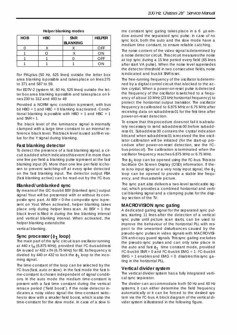
Helper blanking modes
For PALplus (50 Hz, 625 lines) outside the letter boxarea blanking is possible and takes place on lines 275to 371 and 587 to 59. For EDTV-2 (system M, 60 Hz, 525 lines) outside the let-ter box area blanking is possible and takes place on li-nes 230 to 312 and 493 to 49Provided a NORM sync condition is present, with busbit HBO = 1 and HBC = 0 blanking is activated. Condi-tional blanking is possible with HBO = 1 and HBC = 1and SNR = 1.The black level of the luminance signal is internallyclamped with a large time constant to an internal re-ference black level. This black level is used as fill-in va-lue for the Y signal during blanking.
Fast blanking detectorTo detect the presence of a fast blanking signal, a cir-cuit is added which indicates this event if in more thanone line per field a blanking pulse is present at the fastblanking input (F). More than one line per field is cho-sen to prevent switching-off at every spike detectedon the fast blanking input. The detector output FBA(fast blanking active) can be read-out by the I2C-bus.
Blanked/unblanked syncBy means of the I2C-bus bit BSY (blanked sync) outputsignal Yout will be presented with or without its com-posite sync part. At BSY = 0 the composite sync is pre-sent on Yout When activated, helper blanking takesplace only during helper lines scan. At BSY = 1 theblack level is filled in during the line blanking intervaland vertical blanking interval. When activated, thehelper blanking extends thevertical blanking.
Sync processor (ϕ1 loop)The main part of the sync circuit is an oscillator runningat 440 x fH (6.875 MHz), provided that I2C-bus address8A is used or 432 x fH (6.75 MHz) for 8E. Its frequency isdivided by 440 or 432 to lock the ϕ1 loop to the inco-ming signal. The time-constant of the loop can be selected by theI2C-bus (fast, auto or slow). In the fast mode the fast ti-me-constant is chosen independent of signal conditi-ons. In the auto mode the medium time-constant ispresent with a fast time constant during the verticalretrace period (‘field boost’). If the noise detector in-dicates a noisy video signal the time-constant switc-hes to slow with a smaller field boost, which is also thetime-constant for the slow mode. In case of a slow ti-
me constant sync gating takes place in a 6 µs win-dow around the separated sync pulse. In case of nosync lock, both the auto and the slow mode have amedium time constant, to ensure reliable catching. The noise content of the video signal is determined bya noise detector circuit. This circuit measures the noiseat top sync during a 15 line period every field (65 linesafter start VA pulse). When the noise level supersedesthe detector threshold in two consecutive fields, noiseis indicated and bus bit SNR is set. The free-running frequency of the oscillator is determi-ned by a digital control circuit that is locked to the ac-tive crystal. When a power-on-reset pulse is detectedthe frequency of the oscillator is switched to a frequ-ency of about 10 MHz (23 kHz horizontal frequency) toprotect the horizontal output transistor. The oscillatorfrequency is calibrated to 6.875 MHz or 6.75 MHz afterreceiving data on subaddress 01 for the first time afterpower-on-reset detection. To ensure that this procedure does not fail it is absolu-tely necessary to send subaddress 00 before subadd-ress 01. Subaddress 00 contains the crystal indicationbits and when subaddress 01 is received the line oscil -lator calibration will be initiated (for the start-up pro-cedure after power-on-reset detection, see the I2C-bus protocol). The calibration is terminated when theoscillator frequency reaches 6.875 MHz or 6.75 MHz. The ϕ1 loop can be opened using the I2C-bus. This is tofacilitate On Screen Display (OSD) information. If the-re is no input signal or a very noisy input signal, the ϕ1loop can be opened to provide a stable line frequ-ency, and thus astable picture.The sync part also delivers a two-level sandcastle sig-nal, which provides a combined horizontal and verti-cal blanking signal and a clamping pulse for the disp-lay section of the TV.
MACROVISION sync gatingA dedicated gating signal for the separated sync pul-ses, starting 11 lines after the detection of a verticalsync pulse until picture scan starts, can be used toimprove the behaviour of the horizontal PLL with res-pect to the unwanted disturbances caused by thepseudo-sync pulses in video signals with MACROVISI-ON anti-copy guard signals. This sync gating excludesthe pseudo-sync pulses and can only take place inthe auto and fast ϕ1 time constant mode, providedI2C-bus bit SNR = 0 and I2C-bus bit EMG = 1. I2C-bus bitEMG = 1 enables and EMG = 0 disables this sync ga-ting in the horizontal PLL.
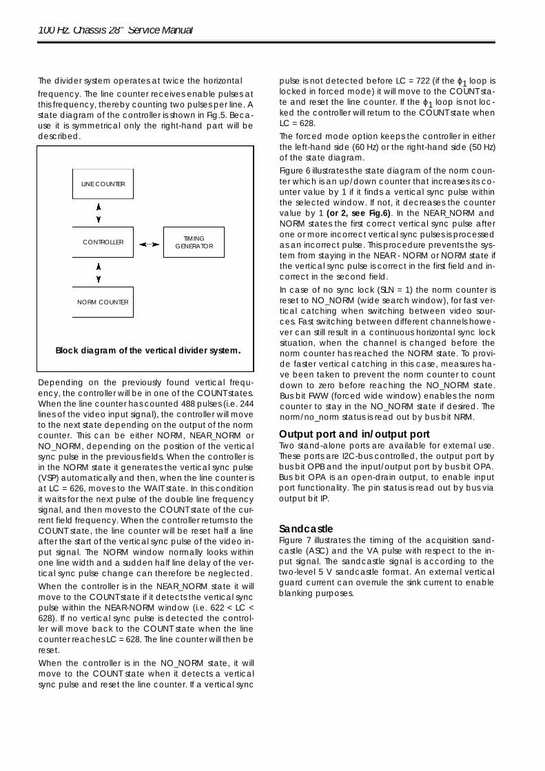
Vertical divider systemThe vertical divider system has a fully integrated verti-cal sync separator. The divider can accommodate both 50 Hz and 60 Hzsystems; it can either determine the field frequencyautomatically or it can be forced to the desired sys-tem via the I2C-bus. A block diagram of the vertical di-vider system is illustrated in the following figure.
HOB HBC SNR HELPERBLANKING
0 X X OFF1 O X ON1 1 0 OFF1 1 1 ON
The divider system operates at twice the horizontalfrequency. The line counter receives enable pulses atthis frequency, thereby counting two pulses per line. Astate diagram of the controller is shown in Fig.5. Beca-use it is symmetrical only the right-hand part will bedescribed.
Depending on the previously found vertical frequ-ency, the controller will be in one of the COUNT states.When the line counter has counted 488 pulses (i.e. 244lines of the video input signal), the controller will moveto the next state depending on the output of the normcounter. This can be either NORM, NEAR_NORM orNO_NORM, depending on the position of the verticalsync pulse in the previous fields. When the controller isin the NORM state it generates the vertical sync pulse(VSP) automatically and then, when the line counter isat LC = 626, moves to the WAIT state. In this conditionit waits for the next pulse of the double line frequencysignal, and then moves to the COUNT state of the cur-rent field frequency. When the controller returns to theCOUNT state, the line counter will be reset half a lineafter the start of the vertical sync pulse of the video in-put signal. The NORM window normally looks withinone line width and a sudden half line delay of the ver-tical sync pulse change can therefore be neglected. When the controller is in the NEAR_NORM state it willmove to the COUNT state if it detects the vertical syncpulse within the NEAR-NORM window (i.e. 622 < LC <628). If no vertical sync pulse is detected the control-ler will move back to the COUNT state when the linecounter reaches LC = 628. The line counter will then bereset. When the controller is in the NO_NORM state, it willmove to the COUNT state when it detects a verticalsync pulse and reset the line counter. If a vertical sync
pulse is not detected before LC = 722 (if the ϕ1 loop islocked in forced mode) it will move to the COUNT sta-te and reset the line counter. If the ϕ1 loop is not loc-ked the controller will return to the COUNT state whenLC = 628. The forced mode option keeps the controller in eitherthe left-hand side (60 Hz) or the right-hand side (50 Hz)of the state diagram. Figure 6 illustrates the state diagram of the norm coun-ter which is an up/down counter that increases its co-unter value by 1 if it finds a vertical sync pulse withinthe selected window. If not, it decreases the countervalue by 1 (or 2, see Fig.6). In the NEAR_NORM andNORM states the first correct vertical sync pulse afterone or more incorrect vertical sync pulses is processedas an incorrect pulse. This procedure prevents the sys-tem from staying in the NEAR - NORM or NORM state ifthe vertical sync pulse is correct in the first field and in-correct in the second field. In case of no sync lock (SLN = 1) the norm counter isreset to NO_NORM (wide search window), for fast ver-tical catching when switching between video sour-ces. Fast switching between different channels howe-ver can still result in a continuous horizontal sync locksituation, when the channel is changed before thenorm counter has reached the NORM state. To provi-de faster vertical catching in this case, measures ha-ve been taken to prevent the norm counter to countdown to zero before reaching the NO_NORM state.Bus bit FWW (forced wide window) enables the normcounter to stay in the NO_NORM state if desired. Thenorm/no_norm status is read out by bus bit NRM.
Output port and in/output port Two stand-alone ports are available for external use.These ports are I2C-bus controlled, the output port bybus bit OPB and the input/output port by bus bit OPA.Bus bit OPA is an open-drain output, to enable inputport functionality. The pin status is read out by bus viaoutput bit IP.
Sandcastle Figure 7 illustrates the timing of the acquisition sand-castle (ASC) and the VA pulse with respect to the in-put signal. The sandcastle signal is according to thetwo-level 5 V sandcastle format. An external verticalguard current can overrule the sink current to enableblanking purposes.
100 Hz. Chassis 28” Service Manual
LINE COUNTER
CONTROLLER
NORM COUNTER
TIMINGGENERATOR
Block diagram of the vertical divider system.
100 Hz. Chassis 28” Service Manual
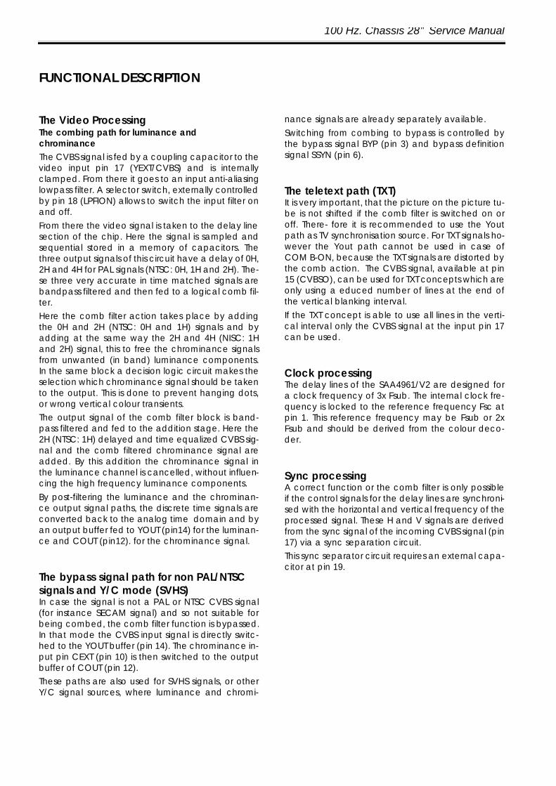
In TV signal processing a comb filter is used to separa-te the chrominance and the luminance signals fromthe CVBS signal without effects such as cross-luminan-ce and cross-colour. The comb filter SAA 4961/V2 shown in figure 3 usestwo 2H delay lines together with an adaptive logicalcomb filter algorithm for processing the PAL standard.In case of NTSC processing two 1H delay lines areused. Effects like hanging dots or residual cross-colo-ur, seen when using a classical comb filter algorithm,are not produced.The switched capacitor delay lines produce threeoutput signals 0H, 2H and 4H (NTSC: 0H, 1H, 2H). Toprevent alias components resulting from the discretetime signal processing, a low-pass pre-filter is integra-
ted in ront. Together with the transversal band-pass filters, the lo-gical comb filter eliminates the luminance compo-nents (in the chrominance frequency band) from thechrominance signal. To eliminate cross-luminance thecomb filtered chrominance is now subtracted fromthe time compensated CVBS signal and convertedby the post filtering to the continuous time domain. Signal switches for an external SVHS signal or non-de-layed CVBS signals are available. They can be cont-rolled externally via BYP (pin 3) and SSYN (pin 6). Internal clock generation only requires a subcarriersignal (fsc or 2 x fsc). Sync separation (SYNC) is inclu-ded for the generation of control signals for the delaylines.
SAA4961Multistandard Comb Filter
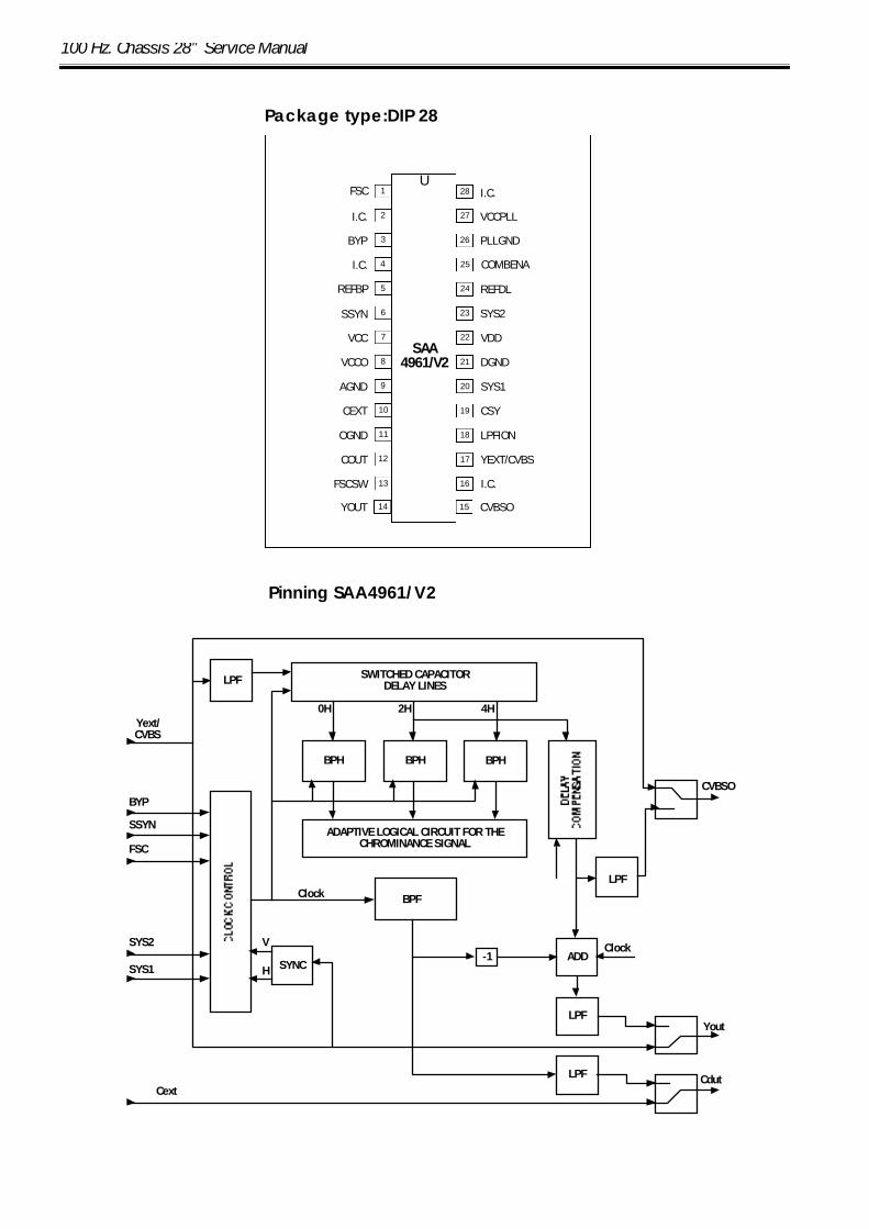
The one-chip Multistandard Comb Filter
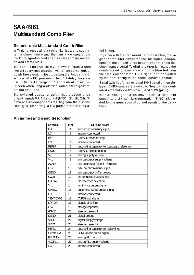
SYMBOL PIN DESCRIPTIONFSC 1 subcarrier frequency inputI.C. 2 internal connectedBYP 3 BYPASS mode forcingI.C. 4 internal connectedREFBP 5 decoupling capacitor for bandpass referenceSSYN 6 BYPASS definition inputVcc 7 analog supply voltageVCCO 8 analog output supply voltageAGND 9 analog ground (signal reference)CEXT 10 external chrominance inputOGND 11 analog output buffer groundCOUT 12 chrominance output signalFSCSW 13 fsc reference selectionYout 14 luminance output signalCVBSO 15 uncombed CVBS output signalI.C. 16 internal connectedYEXT/CVBS 17 CVBS input signalLPFION 18 disable alias filterCSY 19 storage capacitorGSYS1 20 standard select 1DGND 21 digital groundVDD 22 digital supply voltageSYS2 23 standard select 2REFDL 24 decoupling capacitor for delay linesCOMBENA 25 COMB mode output signalPLLGND 26 analog PLL groundVCCPLL 27 analog PLL supply voltageI.C. 28 internal connected
Pin names and shord description
100 Hz. Chassis 28” Service Manual
1
2
3
4
5
6
7
28
27
26
25
24
23
22
FSC
I.C.
BYP
I.C.
REFBP
SSYN
VCC
U
Package type:DIP 28
I.C.
VCCPLL
PLLGND
COMBENA
REFDL
SAA4961/V2
SYS2
VDD
8 21VCCO DGND
9 20AGND SYS1
10 19CEXT CSY
11 18OGND LPFION
12 17COUT YEXT/CVBS
13 16FSCSW I.C.
14 15YOUT CVBSO
LPF SWITCHED CAPACITORDELAY LINES
0H 2H 4H
BPHBPH
ADAPTIVE LOGICAL CIRCUIT FOR THECHROMINANCE SIGNAL
BPH
SYNC
V
H
Clock BPF
ADD
LPF
LPF
LPF
CVBSO
Yout
Cdut
-1Clock
Cext
SYS1
SYS2
FSC
SSYN
BYP
Yext/CVBS
Pinning SAA4961/V2
100 Hz. Chassis 28” Service Manual
FUNCTIONAL DESCRIPTION
The Video ProcessingThe combing path for luminance and chrominance The CVBS signal is fed by a coupling capacitor to thevideo input pin 17 (YEXT/CVBS) and is internallyclamped. From there it goes to an input anti-aliasinglowpass filter. A selector switch, externally controlledby pin 18 (LPFION) allows to switch the input filter onand off. From there the video signal is taken to the delay linesection of the chip. Here the signal is sampled andsequential stored in a memory of capacitors. Thethree output signals of this circuit have a delay of 0H,2H and 4H for PAL signals (NTSC: 0H, 1H and 2H). The-se three very accurate in time matched signals arebandpass filtered and then fed to a logical comb fil-ter. Here the comb filter action takes place by addingthe 0H and 2H (NTSC: 0H and 1H) signals and byadding at the same way the 2H and 4H (NISC: 1Hand 2H) signal, this to free the chrominance signalsfrom unwanted (in band) luminance components.In the same block a decision logic circuit makes theselection which chrominance signal should be takento the output. This is done to prevent hanging dots,or wrong vertical colour transients. The output signal of the comb filter block is band-pass filtered and fed to the addition stage. Here the2H (NTSC: 1H) delayed and time equalized CVBS sig-nal and the comb filtered chrominance signal areadded. By this addition the chrominance signal inthe luminance channel is cancelled, without influen-cing the high frequency luminance components. By post-filtering the luminance and the chrominan-ce output signal paths, the discrete time signals areconverted back to the analog time domain and byan output buffer fed to YOUT (pin14) for the luminan-ce and COUT (pin12). for the chrominance signal.
The bypass signal path for non PAL/NTSCsignals and Y/C mode (SVHS) In case the signal is not a PAL or NTSC CVBS signal(for instance SECAM signal) and so not suitable forbeing combed, the comb filter function is bypassed.In that mode the CVBS input signal is directly switc-hed to the YOUT buffer (pin 14). The chrominance in-put pin CEXT (pin 10) is then switched to the outputbuffer of COUT (pin 12). These paths are also used for SVHS signals, or otherY/C signal sources, where luminance and chromi-
nance signals are already separately available.Switching from combing to bypass is controlled bythe bypass signal BYP (pin 3) and bypass definitionsignal SSYN (pin 6).
The teletext path (TXT) It is very important, that the picture on the picture tu-be is not shifted if the comb filter is switched on oroff. There- fore it is recommended to use the Youtpath as TV synchronisation source. For TXT signals ho-wever the Yout path cannot be used in case ofCOM B-ON, because the TXT signals are distorted bythe comb action. The CVBS signal, available at pin15 (CVBSO), can be used for TXT concepts which areonly using a educed number of lines at the end ofthe vertical blanking interval. If the TXT concept is able to use all lines in the verti-cal interval only the CVBS signal at the input pin 17can be used.
Clock processing The delay lines of the SAA4961/V2 are designed fora clock frequency of 3x Fsub. The internal clock fre-quency is locked to the reference frequency Fsc atpin 1. This reference frequency may be Fsub or 2xFsub and should be derived from the colour deco-der.
Sync processing A correct function or the comb filter is only possibleif the control signals for the delay lines are synchroni-sed with the horizontal and vertical frequency of theprocessed signal. These H and V signals are derivedfrom the sync signal of the incoming CVBS signal (pin17) via a sync separation circuit. This sync separator circuit requires an external capa-citor at pin 19.
100 Hz. Chassis 28” Service Manual
u 5 V supply voltage, low power consumptionu Active carrier generation by FPLL principle (frequ-
ency-phase-locked-loop) for true synchronous de-modulation
u Very linear video demodulation, good pulse res-ponse and excellent intermodulation figures
u VCO circuit is operating on picture carrier frequ-ency, the VCO frequency is switchable for the L`mode
u Alignment free AFC without external reference cir-cuit, polarity of the AFC curve is switchable
u VIF AGC for negative modulated signals (peaksync. detection) and for positive modulation (peakwhite/black level detector)
u Tuner AGC with adjustable take over pointu Alignment free quasi parallel sound (QPS) mixer for
FM/NICAM sound IF signalsu Intercarrier output signals is gain controlled (neces-
sary for digital sound processing)u Complete alignment-free AM demodulator with
gain controlled AF outputu Separate SIF-AGC with average detection u Two independent SIF inputsu Parallel operation of the AM demodulator and
QPS mixer (for NICAM L stereo sound) u Package and relevant pinning is compatible with
the single standard version TDA4472, which simplifi-es the design of an universal IF module
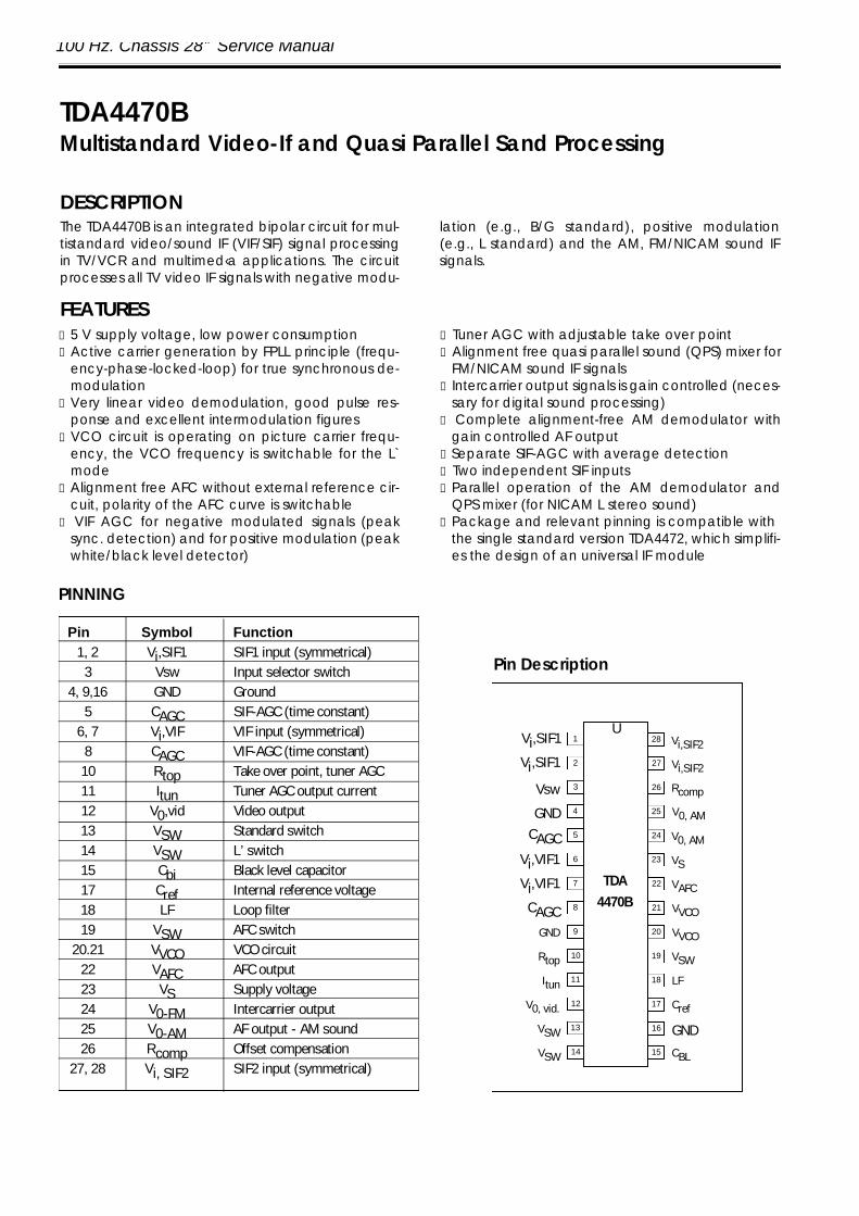
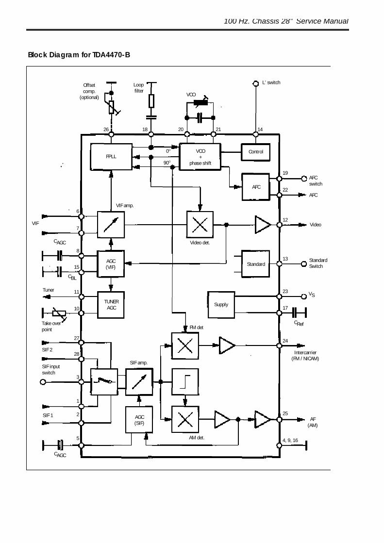
TDA4470BMultistandard Video-If and Quasi Parallel Sand Processing
The TDA4470B is an integrated bipolar circuit for mul-tistandard video/sound IF (VIF/SIF) signal processingin TV/VCR and multimed‹a applications. The circuitprocesses all TV video IF signals with negative modu-
lation (e.g., B/G standard), positive modulation(e.g., L standard) and the AM, FM/NICAM sound IFsignals.
DESCRIPTION
FEATURES
Pin Symbol Function1, 2 Vi,SIF1 SIF1 input (symmetrical)
3 Vsw Input selector switch4, 9,16 GND Ground
5 CAGC SIF-AGC (time constant) 6, 7 Vi,VIF VIF input (symmetrical)
8 CAGC VIF-AGC (time constant) 10 Rtop Take over point, tuner AGC11 Itun Tuner AGC output current 12 V0,vid Video output 13 VSW Standard switch14 VSW L’ switch 15 Cbi Black level capacitor 17 Cref Internal reference voltage18 LF Loop filter 19 VSW AFC switch
20.21 VVCO VCO circuit 22 VAFC AFC output 23 VS Supply voltage 24 V0-FM Intercarrier output 25 V0-AM AF output - AM sound 26 Rcomp Offset compensation
27, 28 Vi, SIF2 SIF2 input (symmetrical)
PINNING
1
2
3
4
5
6
7
28
27
26
25
24
23
22
Vi,SIF1
Vi,SIF1
Vsw
GNDCAGC
Vi,VIF1
Vi,VIF1
U
Pin Description
Vi,SIF2
Vi,SIF2
Rcomp
V0, AM
V0, AM
VS
VAFC
8 21CAGC VVCO
9 20GND VVCO
10 19Rtop VSW
11 18Itun LF
12 17V0, vid. Cref
13 16VSW GND14 15VSW CBL
TDA4470B
100 Hz. Chassis 28” Service Manual
Offsetcomp.
(optional)
Loopfilter
FPLL
AGC(VIF)
AGC(SIF)
TUNERAGC
Supply
Standard
AFC
ControlVCO+
phase shift
26
6
7
CAGC
CBL
Tuner
SIF 2
SIF 1
CAGC
SIF inputswitch
Take overpoint
8
15
11
10
27
28
3
1
2
5
18
VIF amp.
Video det.
SIF amp.
FM detCRef
VS
AM det. 4, 9, 16
25
24
17
23
13
12
22
19
14
AFC
AFCswitch
Video
StandardSwitch
AF(AM)
Intercarrier(FM / NICAM)
VIF
0O
90O
20
VCO
L’ switch
21
Block Diagram for TDA4470-B
100 Hz. Chassis 28” Service Manual
Vision IF AmplifierThe video IF signal (VIF) is fed through a SAW filter to the differential input (Pin 6-7) of theVIF amplifier. This amplifier consists of three AC-coupled amplifier stages. Each differen-tial amplifier is gain controlled by the automatic gain control (VIF-AGC). The output sig-nal of the VIF amplifier is applied to the FPLL carrier generation and the video demodu-lator.
Tuner-and VIF-AGCAt Pin 8, the VIF-AGC charges/discharges the AGC capacitor to generate a controlvoltage for setting the gain of the VIF amplifier and tuner in order to keep the video out-put signal at a constant level. Therefore, in the case of all negative modulated signals(e.g., B/G standard) the sync. level of the demodulated video signal is the criterion fora fast charge/discharge of the AGC capacitor. For positive modulation (e.g., L stan-dard) the peak white level of video signal controls the charge current. In order to redu-ce reaction time for positive modulation, where a large time constant is needed, anadditional black level detector controls the discharge current in the event of decre-asing VIF input signal. The control voltage (AGC voltage at Pin 8) is transferred to an in-ternal control signal, and is fed to the tuner AGC to generate the tuner AGC current atPin 11 (open collector output). The take over point of the tuner AGC can be adjustedat Pin 10 by a potentiometer or an external de voltage (from interface circuit or mic-roprocessor).
FPLL,VCO and AFCThe FPLL circuit (frequency phase locked loop) consists of a frequency and phase de-tector to generate the control voltage for the VCO tuning. In the locked mode, theVCO is controlled by the phase detector and in unlocked mode, the frequency de-tector is superimposed. The VCO operates with an external resonance circuit (L and Cparallel) and is controlled by internal varicaps. The VCO control voltage is also conver-ted to a current and represents the AFC output signal at Pin 22. At the AFC switch (Pin19) three operating conditions of the AFC are possible: AFC curve “rising” or “falling”and AFC “off’.
A practicable VCO alignment of the external coil is the adjustment to zero AFC outputcurrent at Pin 22. At center frequency the AFC output current is equal to zero. Further-more. at Pin 14. the VCO center frequency can be switched for setting to the requiredL’ value (L’ standard).
The optional potentiometer at Pin 26 allows an offset compensation of the VCO phasefor improved sound quality (fine adjustment). Without a potentiometer (open circuitat Pin 26). this offset compensation is not active.
The oscillator signal passes a phase shifter and supplies the in-phase signal (0o) and thequadrature signal (90o)of the generated picture carrier.
Video Demodulation and Amplifier The video IF signal, which is applied from the gain controlled IF amplifier, is multipliedwith the inphase component of the VCO signal. The video demodulator is designed forlow distortion and large bandwidth. The demodulator output signal passes an integra-ted low pass filter for attenuation of the residual vision carrier and is fed to the videoamplifier. The video amplifier is realized by an operational amplifier with internal feed-back and 8 MHz bandwidth (-3 dB). A standard dependent de level shift in this stagedelivers the same sync. level for positive and negative modulation. An additional noiseclipping is provided. The video signal is fed to VlF-AGC and to the video output buffer.This amplifier with a 6 dB gain offers easy adaption of the sound trap. For nominal video
CIRCUIT DESCRIPTION
100 Hz. Chassis 28” Service Manual
IF modulation the video output signal at Pin 12 is 2 Vpp.
Sound IF Amplifier and SIF-AGCThe SIF amplifier is nearly identical with the 3-stage VIF amplifier. Only the first amplifierstage exists twice and is switchable by a control voltage at Pin 3. Therefore with a mi-nimal external expense it is possible to switch between two different SAW filters. Both SIFinputs features excellent cross-talk attenuation and an input impedance which is inde-pendent from the switching condition.
The SIF-AGC is related to the average level of AM- or FM-carrier and controls the SIFamplifier to provide a constant SIF signal to the AM demodulator and QPS mixer.
AM DemodulatorThe alignment-free AM demodulator is realized by a synchronous detector. The modu-lated SIF signal from the SIF amplifier output is multiplied in phase with the limited SIF sig-nal (AM is removed). The AF signal of the demodulator output is fed to the output amp-lifier and to the SIF-AGC. For all TV standards with negative video modulation (eg., B/Gstandard). the AF output signal (Pin 25) is switched off by the standard switch.
Quasi-Parallel-Sound (QPS) MixerThe QPS mixer i~ realized by a multiplier. The signal (FM or NICAM carrier) is convertedto the intercarrier frequency by the regenerated picture carrier frequency by the rege-nerated picture carrier (quadrature signal) which is provided from the VCO. The inter-carrier signal is fed via an output amplifier to Pin 24.
Standard SwitchTo have equal polarity of the video output signal the polarity can be switched inthe demodulation stage in accordance with the TV standard. Additional a stan-dard dependent de level shift in the video amplifier delivers the same sync. level.In parallel to this, the correct VIF-AGC is selected for positive or negative modula-ted VIF signals. In the case of negative modulation (e.g., B/G standard) the AMoutput signal is switched off. For positive modulation (L standard) the AM demodu-lator and QPS mixer is active. This condition allows a parallel operation of the AMsound signal and the NICAM-L stereo sound.
L’Switch With a control voltage at Pin 14 the VCO frequency can be switched for setting tothe required L’ value (L’ standard). Also a fine adjustment of the L’-VCO center fre-quency is possible via a potentiometer. The L’ switch is only active for positive mo-dulated video IF-signals (standard switch in L mode).
AFC Switch The AFC output signal at Pin 22 can be controlled by a switching voltage at Pin 19.It is possible to select an AFC output signal with a rising-or falling AFC curve and toswitch off the AFC.
VCR Mode For the VCR mode in a TV set (external video source selected), it is recommendab-le to switch off the IF circuit. With an external switching voltage at Pin 6 or 7, the IFamplifiers are switched off and all signal output levels at Pins 12, 24, and 25 are ac-cording to the internal de voltage.
Internal Voltage StabilizerThe internal bandgap reference ensures constant performance independent ofsupply voltage and temperature.
100 Hz. Chassis 28” Service Manual
TDA9151BProgrammable Deflection Controller
The TDA9151B is a programmable deflection control-ler contained in a 20-pin DIP package and construc-ted using BIMOS technology. This high performance synchronization and DC def-lection processor has been especially designed foruse in both digital and analog based TV receiversand monitors, and serves horizontal and vertical def-lection functions for all TV standards.
The TDA9151B uses a line-locked clock at 6.75, 13.5or 27 MHz, depending on the line frequency andapplication, and requires only a few external com-ponents. The device can be programmed in a self-adaptive mode or in a programmable fixed slopemode. Selection of these modes and a large num-ber of other functions is fully programmable via theI2C-bus.
GENERAL DESCRIPTION
Generalu 6.75, 13.5 and 27 MHz clock frequencyu Few external componentsu Synchronous logicu I2C-bus controlledu Easy interfacingu Low poweru ESD protectionu Flash detection with restartu Two-level sandcastle pulse.
Vertical deflectionu 16-bit precision vertical scanu Self adaptive or programmable fixed slope modeu DC coupled deflection to prevent picture boun-
ceu Programmable fixed compression to 75%u Programmable vertical expansion in the fixed
slope modeu S-correction can be presetu S-correction setting independent of the field
frequencyu Differential output for high DC stabilityu Current source outputs for high EMC immunityu Programmable de-interlace phase.
East-West correctionu DC coupled EW correction to prevent picture
bounceu 2nd and 4th order geometry correction can be
presetu Trapezium correctionu Geometry correction settings are independent of
field frequencyu Self adaptive Bult generator prevents ringing of
the horizontal deflectionu Current source output for high EMC immunity.
Horizontal deflectionu Phase 2 loop with low litteru Internal loop filteru Dual slicer horizontal flyback inputu Soft start by I 2C-busu Over voltage protection/detection with selection
and status bit.
EHT correctionu Input selection between aquadag or EHT bleederu Internal filter.
FEATURES
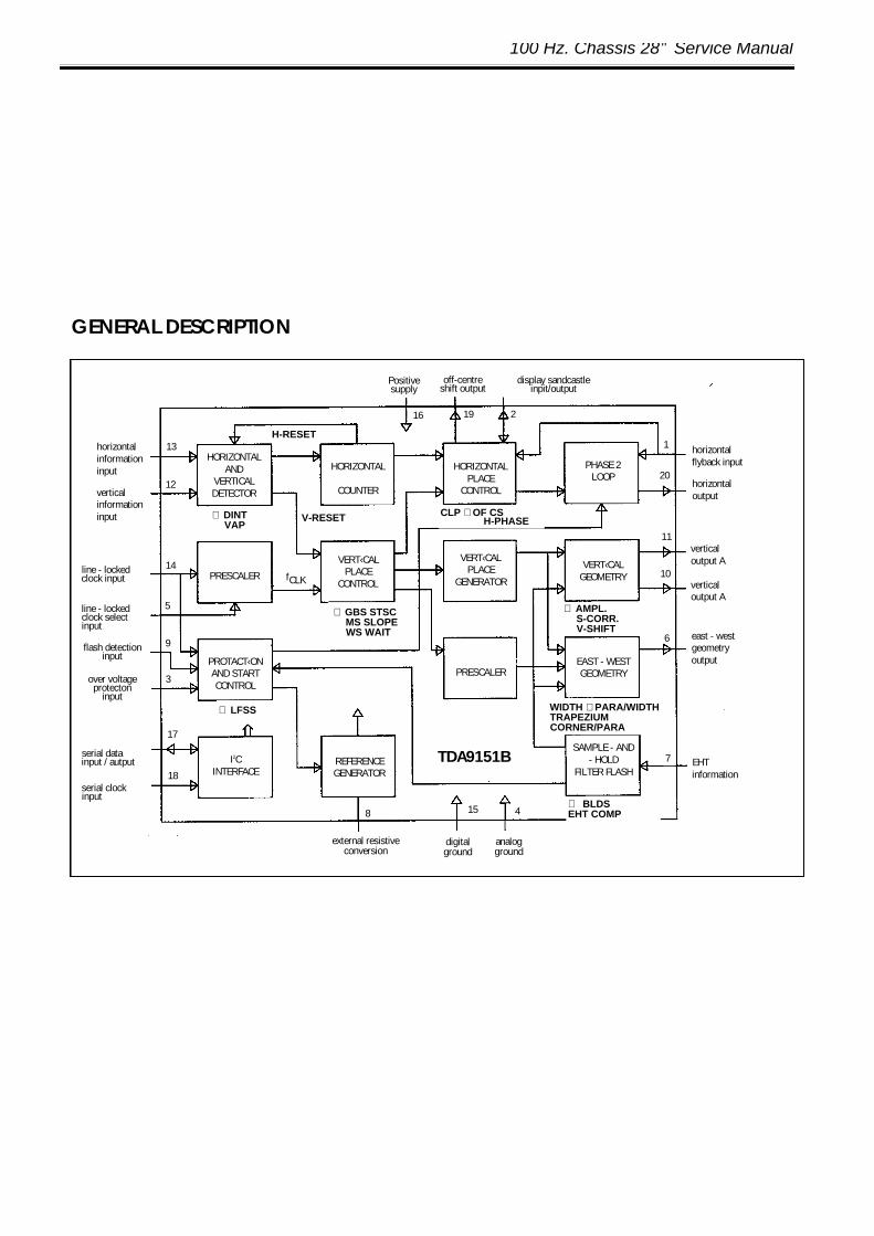
100 Hz. Chassis 28” Service Manual
GENERAL DESCRIPTION
horizontalinformationinput
verticalinformationinput
13
12
HORIZONTALAND
VERTICALDETECTOR
PRESCALERline - lockedclock input
line - lockedclock selectinput
flash detectioninput
over voltageprotecton
input
serial datainput / autput
serial clockinput
14
5
9
3
17
18
PROTACT‹ONAND STARTCONTROL
horizontalflyback input
horizontaloutput
verticaloutput A
verticaloutput A
east - westgeometryoutput
EHTinformation
I2CINTERFACE
REFERENCEGENERATOR
T D A 9 1 5 1 B
VERT‹CALPLACE
GENERATOR
PRESCALER
HORIZONTALPLACE
CONTROL
VERT‹CALPLACE
CONTROL
HORIZONTAL
COUNTER
PHASE 2LOOP
VERT‹CALGEOMETRY
EAST - WESTGEOMETRY
SAMPLE - AND- HOLD
FILTER FLASH
CLP ⇑ OF CSH-PHASE
⇑ AMPL.S-CORR.V-SHIFT
7
6
10
11
20
1
WIDTH ⇑ PARA/WIDTHTRAPEZIUMCORNER/PARA
⇑ BLDSEHT COMP
analogground
digitalground
external resistiveconversion
8 415
⇑ GBS STSCMS SLOPEWS WAIT
fCLK
⇑ DINTVAP
V-RESET
⇑ LFSS
H-RESET
16 19 2
Positivesupply
off-centreshift output
display sandcastleinpit/output
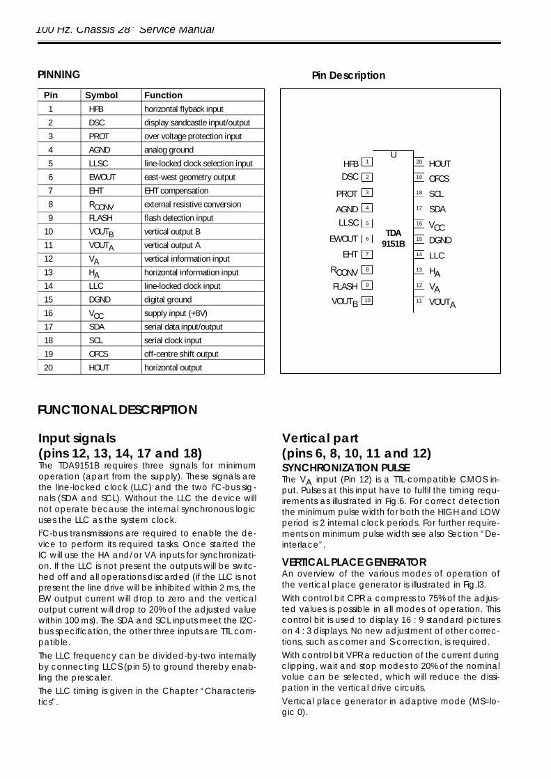
100 Hz. Chassis 28” Service Manual
Pin Symbol Function1 HFB horizontal flyback input
2 DSC display sandcastle input/output
3 PROT over voltage protection input
4 AGND analog ground
5 LLSC line-locked clock selection input
6 EWOUT east-west geometry output
7 EHT EHT compensation
8 RCONV external resistive conversion
9 FLASH flash detection input
10 VOUTB vertical output B
11 VOUTA vertical output A
12 VA vertical information input
13 HA horizontal information input
14 LLC line-locked clock input
15 DGND digital ground
16 VCC supply input (+8V)
17 SDA serial data input/output
18 SCL serial clock input
19 OFCS off-centre shift output
20 HOUT horizontal output
PINNING
1
2
3
4
5
6
7
20
19
18
17
16
15
14
HFBDSC
PROT
AGNDLLSC
EWOUT
EHT
U
Pin Description
HOUT
OFCS
SCL
SDA
VCCDGND
LLC8 13RCONV HA9 12FLASH VA10 11VOUTB VOUTA
TDA9151B
FUNCTIONAL DESCRIPTION
Input signals (pins 12, 13, 14, 17 and 18)The TDA9151B requires three signals for minimumoperation (apart from the supply). These signals arethe line-locked clock (LLC) and the two I2C-bus sig-nals (SDA and SCL). Without the LLC the device willnot operate because the internal synchronous logicuses the LLC as the system clock. I2C-bus transmissions are required to enable the de-vice to perform its required tasks. Once started theIC will use the HA and/or VA inputs for synchronizati-on. If the LLC is not present the outputs will be switc-hed off and all operations discarded (if the LLC is notpresent the line drive will be inhibited within 2 ms, theEW output current will drop to zero and the verticaloutput current will drop to 20% of the adjusted valuewithin 100 ms). The SDA and SCL inputs meet the I2C-bus specification, the other three inputs are TTL com-patible. The LLC frequency can be divided-by-two internallyby connecting LLCS (pin 5) to ground thereby enab-ling the prescaler. The LLC timing is given in the Chapter “Characteris-tics”.
Vertical part (pins 6, 8, 10, 11 and 12) SYNCHRONIZATION PULSEThe VA input (Pin 12) is a TTL-compatible CMOS in-put. Pulses at this input have to fulfil the timing requ-irements as illustrated in Fig.6. For correct detectionthe minimum pulse width for both the HIGH and LOWperiod is 2 internal clock periods. For further require-ments on minimum pulse width see also Section “De-interlace”.
VERTICAL PLACE GENERATORAn overview of the various modes of operation ofthe vertical place generator is illustrated in Fig.l3.With control bit CPR a compress to 75% of the adjus-ted values is possible in all modes of operation. Thiscontrol bit is used to display 16 : 9 standard pictureson 4 : 3 displays. No new adjustment of other correc-tions, such as corner and S-correction, is required. With control bit VPR a reduction of the current duringclipping, wait and stop modes to 20% of the nominalvolue can be selected, which will reduce the dissi-pation in the vertical drive circuits.Vertical place generator in adaptive mode (MS=lo-gic 0).
100 Hz. Chassis 28” Service Manual
The vertical start-scan data (subaddress 02) determi-nes the vertical placement in the total range of 64 x432 clock periods in 63 steps. The maximum numberof synchronized lines per scan is 910 with an equiva-lent field frequency of 17.2 or 34.4 Hz for fH = 15625or 31250 Hz respectively. The minimum number of synchronized lines per scanis 200 with an equivalent field frequency of 78 or 156Hz for fH = 15 625 or 31250 Hz respectively. If the VA pulse is not present, the number of lines perscan will increase to 910.2. If the LLC is not presentthe vertical blanking will start within 2 µs.Amplitude control is automatic, with a settling timeof 1 to 2 new fields and an accuracy of either 16/12or 48/12 lines depending on the value of the GBS bit.Differences in the number of lines per field, as canoccur in TXT or in multi-head VTR, will not affect theamplitude setting providing the differences are lessthan the value selected with GBS. This is called amp-litude control guardband. This difference sequenceand the difference sequence length are not impor-tant.Vertical place generator in constant slope mode(MS = logic I) In this mode the slope can be programmed directlywith a two byte value on subaddress 0C (MSB) and0D (LSB). When the actual number of lines is greaterthan the programmed number of lines, the circuitwill enter the stop state in which the differential ver-tical output current remains 100% or drops to 20%(programmable with control bit VPR). The program-med value for the slope is the required number of li-nes multiplied by 72. The programming limits are; mi-nimum 200 x 72 and maximum 910 x 72.A vertical expansion is obtained with a combinationof slope data and a programmable wait status, atsubaddress 0E. The wait status is selected with cont-rol bit MS and can only be activated in the constantslope mode. The wait state is an 8-bit value, prog-rammable from 0 to 255. The actual wait state is oneline longer than the programmed value. If blankingis applied during stop and wait status the differentialoutput current will be the same with VPR selectedvalue (20 or 100%).
DE-INTERLACEWith de-interlace on (DINT = logic 0), the VA pulse issampled with LLC at a position supplied by controlbit DIP (de-interlace phase). When DIP = logic 0 sampling takes place 42 clockpulses after the leading edge of HA (T = Tline x42/432). When DIP = logic 1 sampling takes place 258 clockpulses after the leading edge of HA (T = Tline x258/432). The distance between the two selectable sampling
points is (Tline x (258 - 42)/432) which is exactly half aline, thus de-interlace is possible in two directions. The duration of the VA pulse must, therefore, be suf-ficient to enable the HA pulse to caught, in thisevent an active time of minimum of half a line.With de-interlace off, the VA pulse is sampled withthe system clock. The leading edge is detected andused as the vertical reset. Selection of the positive ornegative leading edge is achieved by the controlbit VAP.
Horizontal part (pins 1,2, 13, 19 and 20
SYNCHRONIZATION PULSE The HA input (pin 13) is a TTL-compatible CMOS in-put. Pulses on this input have to fulfil the timing requ-irements as illustrated in Fig.6. For correct detectionthe minimum pulse width for both the HIGH and LOWperiods is 2 internal clock periods.
FLYBACK INPUT PULSEThe HFB input (pin 1) is a CMOS input. The delay ofthe centre of the flyback pulse to the leading edgeof the HA pulse can be set via the I2C-bus with thehorizontal phase byte (subaddress 08) The resolutionis 6-bit.
OUTPUT PULSEThe HOUT pulse (pin 20) is an open-drain NMOS out-put. The duty factor for this output is typically 52/48(conducting/non-conducting) during normal opera-tion. A soft start causes the duty factor to increase li-nearly from 5 to 52% over a minimum period of 2000lines in 2000 steps.
OFF-CENTRE SHIFTThe OFCS output (pin 19) is a push-pull CMOS outputwhich is driven by a pulse-width modulated DAC. By using a suitable interface, the output signal canbe used for off-centre shift correction in the horizon-tal output stage. This correction is required for HDTVtubes with a 16 x 9 aspect ratio and is useful for highperformance flat square tubes to obtain the requ-ired horizontal linearity. For applications where off-centre correction is not required, the output can beused as an auxiliary DAC. The OFCS signal is phase-locked with the line frequency. The off-centre shiftcan be set via the I2C-bus, subaddress 09, with a 6-bit resolution as illustrated in Fig.8.
SANDCASTLEThe DSC input/output (pin 2) acts as a sandcastlegenerating output and a guard sensing input. As anoutput it provides 2 levels (apart from the base le-vel), one for the horizontal and vertical blanking andthe other for the video clamping. As an input it actsas a current sensor during the vertical blanking inter-val for guard detection.
CLAMPING PULSE
100 Hz. Chassis 28” Service Manual
The clamping pulse width is 21 internal clock periods.The shift, with respect to HA can be varied from 35 to49 clock periods in 7 steps via the I2C-bus, clampshift byte subaddress 0A, as illustrated in Fig.9. It ispossible to suppress the clamping pulse during wait,stop and protection modes with control bit CSU. Thiswill avoid unwanted reset of the TDA4680/81 (onlyused in those circuits).
HORIZONTAL BLANKINGThe start of the horizontal blanking pulse is minimum38 and maximum 41 clock periods before the cent-re of the flyback pulse, depending on the fclk/fH ra-tio K in accordance with 41 - (432 - K). Stop of the horizontal blanking pulse is determinedby the trailing edge of the HFB pulse at the horizon-tal blanking slicing level.
VERTICAL BLANKINGThe vertical blanking pulse starts two internal clockpulses after the rising edge of the VA pulse. Duringthis interval a small guard pulse, generated duringflyback by the vertical power output stage, must beinserted. Stop vertical blanking is effected at theend of the blanking interval only when the guardpulse is present (see Section “Vertical guard”).The start scan setting determines the end of verticalblanking with a 6-bit resolution in steps of one line viathe I2C-bus subaddress 02.
VERTICAL GUARDIn the vertical blanking interval a small unblankingpulse is inserted. This pulse must be filled-in by a blan-king pulse or guard pulse from the vertical poweroutput stage which was generated during the fly-back period. In this condition the sandcastle outputacts as guard detection input and requires a mini-mum 800 µA input current. This current is sensed du-ring the unblanking period. Vertical blanking is onlystopped at the end of the blanking interval whenthe inserted pulse is present. In this way the picturetube is protected against damage in the event ofmissing or malfunctioning vertical deflection
VERTICAL GEOMETRY PROCESSINGThe vertical geometry processing is DC-coupled andtherefore independent of field frequency. The exter-nal resistive conversion (RCONV) at pin 8 sets the re-ference current for both the vertical and EW ge-ometry processing. A useful range is 100 to 150 µA,the recommended value is 120 µA.
VERTICAL OUTPUTSThe vertical outputs VOUTA and VOUTB on pins 10and 11 together form a differential current output.The vertical amplitude can be varied over the range80 to 120% in 63 steps via the I2C-bus (subaddress 00).Vertical S-correction is also applied to these outputsand can be set from 0 to 16% by subaddress 01 witha 6-bit resolution.
The vertical off-centre shift (OFCS) shifts the verticaldeflection current zero crossing with respect to theEW parabola bottom. The control range is -1.5 to+1.5% (±1/8 x I8) in 7 steps set by the least significantnibble at subaddress 03.
EW GEOMETRY PROCESSINGThe EW geometry processing is DC coupled and the-refore independent of field frequency. RCONV setsthe reference current for both the vertical and EWgeometry processing. The EW output is an ESD-protected single-ended cur-rent output. The EW width/width ratio can be set from 100 to 80%in 63 steps via subaddress 04 and the EW parabo-la/width ratio from 0 to 20% via subaddress 05. TheEW corner/EW parabola ratio has a control range of-40 to 0% in 63 steps via subaddress 06. The EW trapezium correction can be set from -1.5 to+1.5% in 7 steps via the most significant nibble at su-baddress 03.
BULT GENERATORThe Bult generator makes the EW waveform continu-ous.
Protection input (pin 3)The protection input (PROT) is a CMOS input.The input voltage must be EHT scaled and has thefollowing characteristics:Two modes of protection are available with the aidof control bit PRD.u With PRD = logic 1 the protection mode is selec-
ted, HOUT will be defeated and the PROT bit inthe status word is set if the input voltage is above3.9 V. Thus the deflection stops and EW output cur-rent is zero, while the vertical output current is re-duced to 20% of the adjusted value. A new start ofthe circuit is I2C-bus controlled with the user softwa-re.
u With PRD = logic 0 the detection mode is selected,HOUT will not be defeated and the over voltage information is only written in the PROT status bit and can be read by the I2C-bus.
All further actions, such as a write of the LFSS bit, areachieved by the I2C-bus. They depend on the con-figuration used and are defined by user software.
Flash detection/protection input (pin 9) The FLASH input is a CMOS input with an internal pull-up current of approximately 8 µA.When a negative-going edge crosses the 0.75 V le-vel a restart will be executed with a soft start of app-roximately. 2000 lines, such as in the soft-start mode.When the function is not used pin 9 can be connec-ted to ground, VCC or left open-circuit, the internalpull-up current source will prevent any problems. Ho-wever a hard wired connection to VCC or ground is
100 Hz. Chassis 28” Service Manual
QUICK REFERENCE DATA
VCC supply voltage 7.2 8.0 8.8 V
ICC supply current fclk= 6.75 MHz - 27 - mA
Ptot total power dissipation top sync-white - 220 - mW
Tamb operating ambient temperature top sync-whit -25 - +70 Co
InputsV14 line-locked clock (LLC) logic level - TTL - -
V13 horizontal sync (HA) logic level - TTL - -
V12 vertical sync (VA) logic level - TTL - -
V5 line-locked clock select (LLCC) logic level note 1 - CMOS 5V - -
V18 serial clock (SCL) logic level - CMOS 5V - -
V17 serial data input (SDA) logic level - CMOS 5V - -
V1 horizontal flyback (HFB) phase FBL = logic 0 - 3.9 - V
slicing level FBL = logic 1 - 1.3 - V
V1 horizontal flyback (HFB) blanking slicing level - 100 - mV
V3 over voltage protection (PROT) level - 3.9 - V
V9 EHT flash detection level - 1.5 - V
OutputsV20 horizontal output (HOUT) voltage (open drain) I20 = 10mA - - 0.5 V
I11-I10(M) vertical differential (VOUTA,B) vertical amplitude =100% 440 475 510 µA
output current (peak value) I8 = -120µA
V10,11 vertical output voltage 0 - 3.9 V
I6(M) EW (EWOUT) total output current (peak value) I8 = -120µA - - 930 µA
V6 EW (EWOUT) output voltage 1.0 - 5.5 V
SANDCASTLE OUTPUT LEVELS (DSC)
V2 base voltage level - 0.5 - V
V2 horizontal and vertical blanking voltage level - 2.5 - V
V2 video blanking voltage leve - 4.5 - V
HORIZONTAL OFF-CENTRE SHIFT (OFCS)
V19 output voltage I19 = 2 mA 0 - VCC V
SYMBOL PARAMETER CONDITIONS Min. Typ. Max. Unit
recommended when the function is not used.
EHT compensation (pin 7)The EHT input is a CMOS input. The EHT compensation input permits scan amplitudemodulation should the EHI supply not be perfect. Forcorrect tracking of the vertical and horizontal def-
lection the gain of the EW output stage, provided bythe ratio RCONV-EW/RCONV, must be 1/16 Vscan XVref .The input for EHT compensation can be derived froman EHT bleeder or from the picture tubes aquadag(subaddress 0B, bit BLDS).
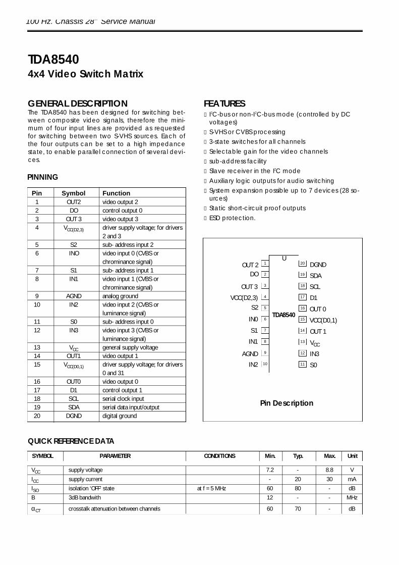
100 Hz. Chassis 28” Service Manual
TDA85404x4 Video Switch Matrix
GENERAL DESCRIPTIONThe TDA8540 has been designed for switching bet-ween composite video signals, therefore the mini-mum of four input lines are provided as requestedfor switching between two S-VHS sources. Each ofthe four outputs can be set to a high impedancestate, to enable parallel connection of several devi-ces.
FEATURESu I2C-bus or non-I2C-bus mode (controlled by DC
voltages)u S-VHS or CVBS processingu 3-state switches for all channelsu Selectable gain for the video channelsu sub-address facilityu Slave receiver in the I2C modeu Auxiliary logic outputs for audio switchingu System expansion possible up to 7 devices (28 so-
urces)u Static short-circuit proof outputsu ESD protection.
Pin Symbol Function1 OUT2 video output 22 DO control output 03 OUT 3 video output 34 VCC(D2,3) driver supply voltage; for drivers
2 and 35 S2 sub- address input 26 INO video input 0 (CVBS or
chrominance signal)7 S1 sub- address input 18 IN1 video input 1 (CVBS or
chrominance signal)9 AGND analog ground10 IN2 video input 2 (CVBS or
luminance signal)11 S0 sub- address input 012 IN3 video input 3 (CVBS or
luminance signal)13 VCC general supply voltage14 OUT1 video output 115 VCC(D0,1) driver supply voltage; for drivers
0 and 3116 OUT0 video output 017 D1 control output 118 SCL serial clock input19 SDA serial data input/output 20 DGND digital ground
PINNING
1
2
3
4
5
6
7
20
19
18
17
16
15
14
OUT 2DO
OUT 3
VCC(D2,3)S2
IN0
S1
U
Pin Description
DGND
SDA
SCL
D1
OUT 0
VCC(D0,1)
OUT 18 13IN1 VCC9 12AGND IN3
10 11IN2 S0
TDA8540
QUICK REFERENCE DATA
VCC supply voltage 7.2 - 8.8 V
ICC supply current - 20 30 mA
ISO isolation ‘OFF’ state at f = 5 MHz 60 80 - dB
B 3dB bandwith 12 - - MHz
αCT crosstalk attenuation between channels 60 70 - dB
SYMBOL PARAMETER CONDITIONS Min. Typ. Max. Unit
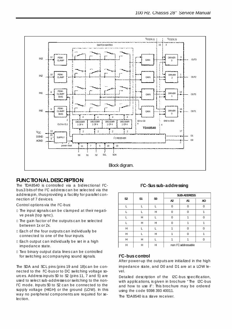
100 Hz. Chassis 28” Service Manual
FUNCTIONAL DESCRIPTIONThe TDA8540 is controlled via a bidirectional I2C-bus.3 bits of the I 2C address can be selected via theaddress pin, thus providing a facility for parallel con-nection of 7 devices.Control options via the I2C-bus:u The input signals can be clamped at their negati-
ve peak (top sync).u The gain factor of the outputs can be selected
between 1x or 2x.u Each of the four outputs can individually be
connected to one of the four inputs.u Each output can individually be set in a high
impedance state.u Two binary output data lines can be controlled
for switching accompanying sound signals.
The SDA and SCL pins (pins 19 and 18)can be con-nected to the I2C-bus or to DC switching voltage so-urces. Address inputs S0 to S2 (pins 11, 7 and 5) areused to select sub-addresses or switching to the non-I2C mode. Inputs S0 to S2 can be connected to thesupply voltage (HIGH) or the ground (LOW). In thisway no peripheral components are required for se-lection.
I2C-bus controlAfter power-up the outputs are initialized in the highimpedance state, and D0 and D1 are at a LOW le-vel.Detailed description of the I2C-bus specification,with applications, is given in brochure “The I2C-busand how to use if’: This brochure may be orderedusing the code 9398 393 40011.The TDA8540 is a slave receiver.
SUB-ADDRESS
A2 A1 AO
L L L 0 0 0
L L H 0 0 1
L H L 0 1 0
L H H 0 1 1
H L L 1 0 0
H L H 1 0 1
H H L 1 1 0
H H H non I2C addressable
S2 S1 S0
I2C-Sus sub-addressing
Block digram.
IN3
IN2
IN1
IN0
VCCDGND
AGND
20
13
9
6
12
10
8
2
CLO to CL1
PEAK-CLAMP/
BIAS
PEAK-CLAMP/
BIAS
PEAK-CLAMP
PEAK-CLAMP
SWITCH MATRIX
GAIN
GAIN
GAIN
GAIN
DRIVER1
DRIVER0
DRIVER2
DRIVER3 OUT3
OUT2
OUT3
OUT1
EN0 to EN3
D0
D1
2
4TDA8540
DECODER1 OF 4
DECODER1 OF 4
DECODER1 OF 4
DECODER1 OF 4
2 2 2 2
4 4 4 4
I2C RECEIVER
S0 S1 S2 SCL SDA
11 7 5 18 19
G0 to G34
SUPPLY
power reset
VCC(D0,1) VCC(D2,3)
15 4
3
1
14
16
17
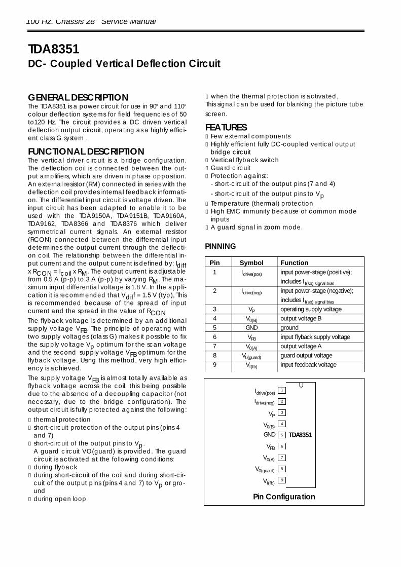
100 Hz. Chassis 28” Service Manual
TDA8351DC- Coupled Vertical Deflection Circuit
GENERAL DESCRIPTIONThe TDA8351 is a power circuit for use in 90o and 110o
colour deflection systems for field frequencies of 50to120 Hz. The circuit provides a DC driven verticaldeflection output circuit, operating as a highly effici-ent class G system .
FUNCTIONAL DESCRIPTIONThe vertical driver circuit is a bridge configuration.The deflection coil is connected between the out-put amplifiers, which are driven in phase opposition.An external resistor (RM) connected in series with thedeflection coil provides internal feedback informati-on. The differential input circuit is voltage driven. Theinput circuit has been adapted to enable it to beused with the TDA9150A, TDA9151B, TDA9160A,TDA9162, TDA8366 and TDA8376 which deliversymmetrical current signals. An external resistor(RCON) connected between the differential inputdetermines the output current through the deflecti-on coil. The relationship between the differential in-put current and the output current is defined by: Idiffx RCON = Icoil x RM. The output current is adjustablefrom 0.5 A (p-p) to 3 A (p-p) by varying RM. The ma-ximum input differential voltage is 1.8 V. In the appli -cation it is recommended that Vdiff = 1.5 V (typ), Thisis recommended because of the spread of inputcurrent and the spread in the value of RCONThe flyback voltage is determined by an additionalsupply voltage VFB. The principle of operating withtwo supply voltages (class G) makes it possible to fixthe supply voltage Vp optimum for the scan voltageand the second supply voltage VFB optimum for theflyback voltage. Using this method, very high effici-ency is achieved. The supply voltage VFB is almost totally available asflyback voltage across the coil, this being possibledue to the absence of a decoupling capacitor (notnecessary, due to the bridge configuration). Theoutput circuit is fully protected against the following: u thermal protectionu short-circuit protection of the output pins (pins 4
and 7) u short-circuit of the output pins to Vp.
A guard circuit VO(guard) is provided. The guardcircuit is activated at the following conditions:
u during flybacku during short-circuit of the coil and during short-cir-
cuit of the output pins (pins 4 and 7) to Vp or gro-und
u during open loop
u when the thermal protection is activated.This signal can be used for blanking the picture tubescreen.
FEATURESu Few external componentsu Highly efficient fully DC-coupled vertical output
bridge circuitu Vertical flyback switchu Guard circuitu Protection against:
- short-circuit of the output pins (7 and 4)- short-circuit of the output pins to Vp
u Temperature (thermal) protectionu High EMC immunity because of common mode
inputsu A guard signal in zoom mode.
Pin Symbol Function1 Idrive(pos) input power-stage (positive);
includes II(sb) signal bias
2 Idrive(neg) input power-stage (negative);includes II(sb) signal bias
3 VP operating supply voltage4 V0(B) output voltage B5 GND ground6 VFB input flyback supply voltage7 V0(A) output voltage A8 V0(guard) guard output voltage9 VI(fb) input feedback voltage
PINNING
1
2
3
4
5
6
7
Idrive(pos)
Idrive(neg)
VP
V0(B)
GND
VFB
V0(A)
U
8V0(guard)
9VI(fb)
TDA8351
Pin Configuration
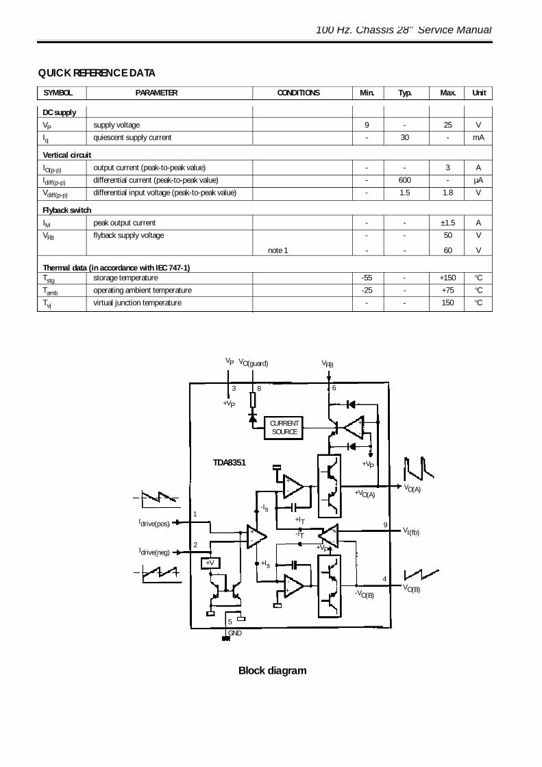
100 Hz. Chassis 28” Service Manual
QUICK REFERENCE DATA
DC supply
VP supply voltage 9 - 25 V
Iq quiescent supply current - 30 - mA
Vertical circuit
IO(p-p) output current (peak-to-peak value) - - 3 A
Idiff(p-p) differential current (peak-to-peak value) - 600 - µA
Vdiff(p-p) differential input voltage (peak-to-peak value) - 1.5 1.8 V
Flyback switch
IM peak output current - - ±1.5 A
VFB flyback supply voltage - - 50 V
note 1 - - 60 V
Thermal data (in accordance with IEC 747-1)Tstg storage temperature -55 - +150 oC
Tamb operating ambient temperature -25 - +75 oC
Tvj virtual junction temperature - - 150 oC
SYMBOL PARAMETER CONDITIONS Min. Typ. Max. Unit
Block diagram
Idrive(pos)1
2
5
+Is
+IT
+VP
-VO(B)VO(B)
VO(A)+VO(A)
VI(fb)
4
9-IT
+VP
VFB
-Is
+V
+-
+-
GND
Idrive(neg)
+VP
3 8 6
VP
CURRENTSOURCE
TDA8351
VO(guard)
+-
+-
+-
100 Hz. Chassis 28” Service Manual
TDA9875ADigital TV Sound Processor (DTVSP)
GENERAL DESCRIPTIONThe TDA9875A is a single-chip Digital TV Sound Pro-cessor (DTVSP) for analog and digital multi-channelsound systems in TV sets and satellite receivers.
Supported standardsThe multistandard/multi-stereo capability of theTDA9875A is mainly of interest in Europe, but also inHong Kong/Peoples Republic of China and SouthEast Asia. This includes B/G, D/K, I, M and L standard.In other application areas there exists only subsets ofthose standard combinations otherwise only singlestandards are transmitted. M standard is transmitted in Europe by the AmericanForces Network (AFN) with European channel spa-cing (7 MHz VHF, 8 MHz UHF) and monaural sound. The AM sound of L/L' standard is normally demodu-lated in the 1 st sound IF. The resulting AF signal hasto be entered into the mono audio input of theTDA9875A. A second possibility is to use the internalAM demodulator stage, however this gives limitedperformance. Korea has a stereo sound system similar to Europeand is supported by the TDA9875A. Differences inc-lude deviation, modulation contents and identifica-tion. It is based on M standard. An overview of the supported standards and soundsystems and their key parameters is given in Table B The analog multi-channel sound systems (A2, A2+and A2*) are sometimes also named 2CS (2 carriersystems).
FEATURESDemodulator and decoder sectionu Sound IF (SIF) input switch e.g. to select between
terrestrial TV SIF and SAT SIF sourcesu SIF AGC with 24 dB control rangeu SIF 8-bit Analog-to-Digital Converter (ADC)u DQPSK demodulation for different standards,
simultaneously with i-channel FM demodulationu NICAM decoding (B/G, I and L standard)u Two-carrier multistandard FM demodulation (B/G,
D/K and M standard)u Decoding for three analog multi-channel systems
(A2, A2+ and A2*) and satellite soundu Optional AM demodulation for system L, simul-
taneously with NICAMu Programmable identification (B/G, D/K and M
standard) and different identification times.
DSP sectionu Digital crossbar switch for all digital signal sources
and destinationsu Control of volume, balance, contour, bass, treble,
pseudo stereo, spatial, bass boost and soft-mute
u Plop-free volume controlu Automatic Volume Level (AVL) controlu Adaptive de-emphasis for satelliteu Programmable beeperu Monitor selection for FM/AM DC values and sig-
nals, with peak detection optionu I2S-bus interface for a feature extension (e.g.
Dolby surround) with matrix, level adjust and mute.
Analog audio sectionu Analog crossbar switch with inputs for mono and
stereo (also applicable as SCART 3 input), SCART 1 input/output, SCART 2 input/output and lineoutput
u User defined full-level/-3 dB scaling for SCART out-puts
u Output selection of mono, stereo, dual A/B, dual A or dual B
u 20 kHz bandwidth for SCART-to-SCART copiesu Standby mode with functionality for SCART copiesu Dual audio digital-to-analog converter from DSP
to analog crossbar switch, bandwidth 15 kHzu Dual audio ADC from analog inputs to DSPu Two dual audio Digital-to-Analog Converters
(DACs) for loudspeaker (Main) and headphone (Auxiliary) outputs; also applicable for L, R, C and S in the Dolby Pro Logic mode with feature ex-tension.
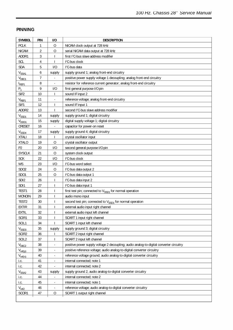
100 Hz. Chassis 28” Service Manual
SYMBOL PIN I/O DESCRIPTION
PCLK 1 O NICAM clock output at 728 kHz
NICAM 2 O serial NICAM data output at 728 kHz
ADDR1 3 I first I2C-bus slave address modifier
SCL 4 I I2C-bus clock
SDA 5 I/O I2C-bus data
VSSA1 6 supply supply ground 1; analog front-end circuitry
VDEC1 7 - positive power supply voltage 1 decoupling; analog front-end circuitry
IREF1 8 - resistor for reference current generator; analog front-end circuitry
P1 9 I/O first general purpose I/O pin
SIF2 10 I sound IF input 2
VREF1 11 - reference voltage; analog front-end circuitry
SIF1 12 I sound IF input 1
ADDR2 13 I second I2C-bus slave address modifier
VSSD1 14 supply supply ground 1; digital circuitry
VDDD1 15 supply digital supply voltage 1; digital circuitry
CRESET 16 - capacitor for power-on reset
VSSD4 17 supply supply ground 4; digital circuitry
XTALI 18 I crystal oscillator input
XTALO 19 O crystal oscillator output
P2 20 I/O second general purpose I/O pin
SYSCLK 21 O system clock output
SCK 22 I/O I2C-bus clock
WS 23 I/O I2C-bus word select
SDO2 24 O I2C-bus data output 2
SDO1 25 O I2C-bus data output 1
SDI2 26 I I2C-bus data input 2
SDI1 27 I I2C-bus data input 1
TEST1 28 I first test pin; connected to VSSD1 for normal operation
MONOIN 29 I audio mono input
TEST2 30 I second test pin; connected to VSSD1 for normal operation
EXTIR 31 I external audio input right channel
EXTIL 32 I external audio input left channel
SCIR1 33 I SCART 1 input right channel
SCIL1 34 I SCART 1 input left channel
VSSD3 35 supply supply ground 3; digital circuitry
SCIR2 36 I SCART 2 input right channel
SCIL2 37 I SCART 2 input left channel
VDEC2 38 - positive power supply voltage 2 decoupling; audio analog-to-digital converter circuitry
Vref(p) 39 - positive reference voltage; audio analog-to-digital converter circuitry
Vref(n) 40 - reference voltage ground; audio analog-to-digital converter circuitry
i.c. 41 - internal connected; note 1
i.c. 42 - internal connected; note 2
VSSA2 43 supply supply ground 2, audio analog-to-digital converter circuitry
i.c. 44 - internal connected; note 2
i.c. 45 - internal connected; note 1
Vref2 46 - reference voltage; audio analog-to-digital converter circuitry
SCOR1 47 O SCART 1 output right channel
PINNING
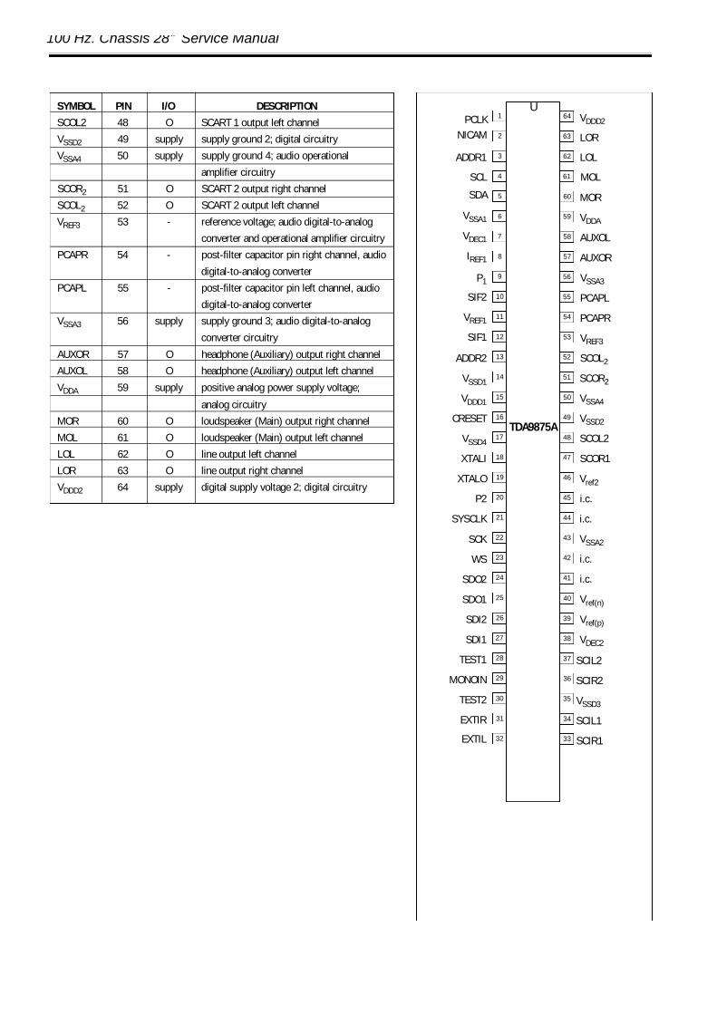
100 Hz. Chassis 28” Service Manual
SYMBOL PIN I/O DESCRIPTION
SCOL2 48 O SCART 1 output left channel
VSSD2 49 supply supply ground 2; digital circuitry
VSSA4 50 supply supply ground 4; audio operational
amplifier circuitry
SCOR2 51 O SCART 2 output right channel
SCOL2 52 O SCART 2 output left channel
VREF3 53 - reference voltage; audio digital-to-analog
converter and operational amplifier circuitry
PCAPR 54 - post-filter capacitor pin right channel, audio
digital-to-analog converter
PCAPL 55 - post-filter capacitor pin left channel, audio
digital-to-analog converter
VSSA3 56 supply supply ground 3; audio digital-to-analog
converter circuitry
AUXOR 57 O headphone (Auxiliary) output right channel
AUXOL 58 O headphone (Auxiliary) output left channel
VDDA 59 supply positive analog power supply voltage;
analog circuitry
MOR 60 O loudspeaker (Main) output right channel
MOL 61 O loudspeaker (Main) output left channel
LOL 62 O line output left channel
LOR 63 O line output right channel
VDDD2 64 supply digital supply voltage 2; digital circuitry
1
2
3
4
5
6
7
64
63
62
61
60
59
58
PCLKNICAM
ADDR1
SCL
SDA
VSSA1
VDEC1
UVDDD2
LOR
LOL
MOL
MOR
VDDA
AUXOL
8 57IREF1 AUXOR
9 56P1 VSSA3
10 55SIF2 PCAPL
11 54VREF1 PCAPR
12 53SIF1 VREF3
13 52ADDR2 SCOL2
14 51VSSD1 SCOR2
15 50VDDD1 VSSA4
16 49CRESET VSSD2
17 48VSSD4 SCOL2
18 47XTALI SCOR1
19 46XTALO Vref2
20 45P2 i.c.
21 44SYSCLK i.c.
22 43SCK VSSA2
23 42WS i.c.
24 41SDO2 i.c.
25 40SDO1 Vref(n)
26 39SDI2 Vref(p)
27 38SDI1 VDEC2
28 37TEST1 SCIL2
29 36MONOIN SCIR2
30 35TEST2 VSSD3
31 34EXTIR SCIL1
32 33EXTIL SCIR1
TDA9875A
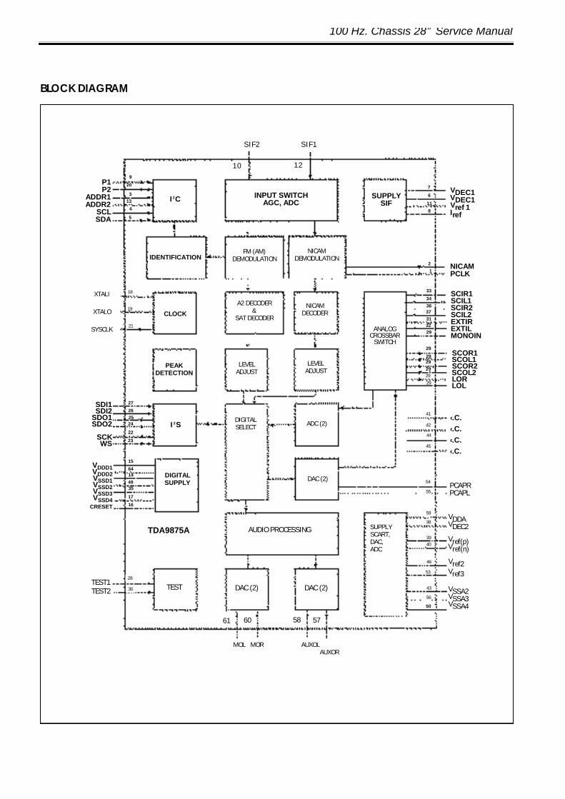
100 Hz. Chassis 28” Service Manual
BLOCK DIAGRAM
VDEC1VDEC1Vref 1Iref
NICAMPCLK
SCIR1SCIL1SCIR2SCIL2EXTIREXTILMONOIN
SCOR1SCOL1SCOR2SCOL2LORLOL
‹.C.‹.C.‹.C.‹.C.
SUPPLYSIF
INPUT SWITCHAGC, ADCI 2C
P1P2
ADDR1ADDR2
SCLSDA
9
20
3
4
5
13
IDENTIFICATION
CLOCK
PEAKDETECTION
I 2S
DIGITALSUPPLY
TDA9875A
VDDD1VDDD2VSSD1VSSD2VSSD3VSSD4
CRESET
15
6414
4935
17
16
SDI1SDI2
SDO1SDO2
SCKWS
27
262524
22
23
7
6
11
8
2
1
33
34
3637313229
29
29292929
29
ANALOGCROSSBAR
SWITCH
S I F 2 S I F 1
1 0 1 2
FM (AM)DEMODULATION
NICAMDEMODULATION
A2 DECODER&
SAT DECODER
LEVELADJUST
LEVELADJUST
NICAMDECODER
DIGITALSELECT ADC (2)
DAC (2)
AUDIO PROCESSING
DAC (2) DAC (2)
MOL MOR AUXOLAUXOR
SUPPLYSCART,DAC,ADC
41
42
44
45
54
55PCAPRPCAPL
VDDAVDEC2
Vref(p)Vref(n)
Vref2Vref3
VSSA2VSSA3VSSA4
XTALI
XTALO
SYSCLK
18
19
21
TEST1TEST2
28
30 TEST
61 60 58 57
59
38
3940
46
53
43
56
50
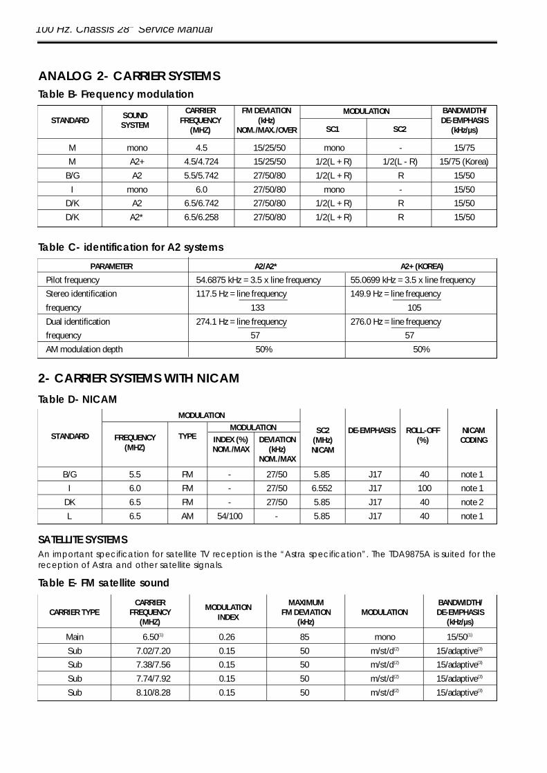
100 Hz. Chassis 28” Service Manual
M mono 4.5 15/25/50 mono - 15/75
M A2+ 4.5/4.724 15/25/50 1/2(L + R) 1/2(L - R) 15/75 (Korea)
B/G A2 5.5/5.742 27/50/80 1/2(L + R) R 15/50
I mono 6.0 27/50/80 mono - 15/50
D/K A2 6.5/6.742 27/50/80 1/2(L + R) R 15/50
D/K A2* 6.5/6.258 27/50/80 1/2(L + R) R 15/50
CARRIERFREQUENCY
(MHZ)
FM DEVIATION(kHz)
NOM./MAX./OVER
BANDWIDTH/DE-EMPHASIS
(kHz/µs)
MODULATION
SC1 SC2STANDARD
SOUNDSYSTEM
ANALOG 2- CARRIER SYSTEMSTable B- Frequency modulation
PARAMETER A2/A2* A2+ (KOREA)
Pilot frequency 54.6875 kHz = 3.5 x line frequency 55.0699 kHz = 3.5 x line frequency
Stereo identification 117.5 Hz = line frequency 149.9 Hz = line frequency
frequency 133 105
Dual identification 274.1 Hz = line frequency 276.0 Hz = line frequency
frequency 57 57
AM modulation depth 50% 50%
Table C- identification for A2 systems
B/G 5.5 FM - 27/50 5.85 J17 40 note 1
I 6.0 FM - 27/50 6.552 J17 100 note 1
DK 6.5 FM - 27/50 5.85 J17 40 note 2
L 6.5 AM 54/100 - 5.85 J17 40 note 1
TYPE INDEX (%)NOM./MAX
DEVIATION(kHz)
NOM./MAX
NICAMCODING
MODULATIONMODULATION SC2
(MHz)NICAM
ROLL-OFF(%)
DE-EMPHASISSTANDARD FREQUENCY
(MHZ)
2- CARRIER SYSTEMS WITH NICAM
SATELLITE SYSTEMS
Table D- NICAM
Main 6.50(1) 0.26 85 mono 15/50(1)
Sub 7.02/7.20 0.15 50 m/st/d(2) 15/adaptive(3)
Sub 7.38/7.56 0.15 50 m/st/d(2) 15/adaptive(3)
Sub 7.74/7.92 0.15 50 m/st/d(2) 15/adaptive(3)
Sub 8.10/8.28 0.15 50 m/st/d(2) 15/adaptive(3)
MODULATIONINDEX
MAXIMUMFM DEVIATION
(kHz)
BANDWIDTH/DE-EMPHASIS
(kHz/µs)MODULATIONCARRIER TYPE
CARRIERFREQUENCY
(MHZ)
Table E- FM satellite sound
An important specification for satellite TV reception is the “Astra specification”. The TDA9875A is suited for thereception of Astra and other satellite signals.
100 Hz. Chassis 28” Service Manual
FUNCTIONAL DESCRIPTION
Description of the demodulator and decoder section
1- SIF INPUTTwo input pins are provided, SIF1 e.g. for ter-restrial TV and SIF2 e.g. for a satellite tuner. Forhigher SIF signal levels the SIF input can be at-tenuated with an internal switchable -10 dBresistor divider. As no specific filters are integ-rated, both inputs have the same specificati-on giving flexibility in application. The selectedsignal is passed through an AGC circuit andthen digitized by an 8-bit ADC operating at24.576 MHz.
2- AGCThe gain of the AGC amplifier is controlledfrom the ADC output by means of a digitalcontrol loop employing hysteresis. The AGChas a fast attack behaviour to prevent ADCoverloads and a slow decay behaviour to pre-vent AGC oscillations. For AM demodulationthe AGC must be switched off. When switc-hed off, the control loop is reset and fixed ga-in settings can be chosen from Table 15 (su-baddress 0). The AGC can be controlled via the I2C-bus.Details can be found in the I2C-bus register de-finitions .(see Chapter 10).
3- MIXERThe digitized input signal is fed to the mixers,which mix one or both input sound carriersdown to zero IF. A 24-bit control word for eachcarrier sets the required frequency. Access tothe mixer control word registers is via the I2C-bus. When receiving NICAM programs, a fe-edback signal is added to the control word ofthe second carrier mixer to establish a carrier-frequency loop.
4- FM AND AM DEMODULATIONAn FM or AM input signal is fed via a band-limi-ting filter to a demodulator that can be usedfor either FM or AM demodulation. Apart fromthe standard (fixed) de-emphasis characteris-tic, an adaptive de-emphasis is available forencoded satellite programs. A stereo deco-der recovers the left and right signal channelsfrom the demodulated sound carriers. Boththe European and Korean stereo systems aresupported.
5- FM IDENTIFICATIONThe identification of the FM sound mode isperformed by AM synchronous demodulation
of the pilot signal and narrow-band detectionof the identification frequencies. The result isavailable via the I2C-bus interface. A selectioncan be made via the I2C-bus for B/G, D/K andM standard and for three different modes thatrepresent different trade-offs between speedand reliability of identification.
6- NICAM DEMODULATIONThe NICAM signal is transmitted in a DQPSK co-de at a bit rate of 728 kbit/s. The NICAM de-modulator performs DQPSK demodulationand feeds the resulting bitstream and clocksignal onto the NICAM decoder and, for eva-luation purposes, to PCLK (pin 1)and NICAM(pin 2). A timing loop controls the frequency of thecrystal oscillator to lock the sampling rate tothe symbol timing of the NICAM data.
7- NICAM DECODERThe device performs all decoding functions inaccordance with the "EBU NICAM 728 specifi-cation”. After locking to the frame alignmentword, the data is descrambled by applyingthe defined pseudo-random binary sequen-ce; the device will then synchronize to the pe-riodic frame flag bit C0.The status of the NICAM decoder can be readout from the NICAM status register by the user(see the I2C-bus register description in Section10.4.2). The OSB bit indicates that the decoderhas locked to the NICAM data. The VDSP bitindicates that the decoder has locked to theNICAM data and that the data is valid sounddata. The C4 bit indicates that the sound con-veyed by the FM mono channel is identical tothe sound conveyed by the NICAM channel.The error byte contains the number of soundsample errors, resulting from parity checking,that occurred in the past 128 ms period. TheBit Error Rate (BER) can be calculated usingthe following equation; bit error
bit errorsBER = __________= error byte x1.74 x 10-5
total bits
8- NICAM AUTO-MUTEThis function is enabled by setting bit AMUTELOW subaddress 14 (see Section 10.3.11). Up-per and lower error limits may be defined bywriting appropriate values to two registers inthe I2C-bus section (subaddresses 16 and 17;see Sections 10.3.13 and 10.3.14). When thenumber of errors in a 128 ms period exceedsthe upper error limit the auto-mute functionwill switch the output sound from NICAM towhatever sound is on the first sound carrier (FM
100 Hz. Chassis 28” Service Manual
or AM). When the error count is smaller thanthe lower error limit the NICAM sound is resto-red.The auto-mute function can be disabled bysetting bit AMUTE HIGH. In this condition clicksbecome audible when the error count incre-ases; the user will hear a signal of degradingquality. A decision to enable/disable the auto-mutingis taken by the microcontroller based on an in-terpretation of the application control bits C1,C2, C3 and C4 and, possibly, any additionalstrategy implemented by the set maker in themicrocontroller software. For NICAM L applications, it is recommendedto demodulate AM sound in the first sound IFand connect the audio signal to the mono in-put of the TDA9875A. By setting the AMSEL bitsubaddress 14 (see Section 10.3.11), the auto-mute function will switch to the audio ADC ins-tead of switching to the first sound carrier.The ADC source selector subaddress 23 (seeSection 10.3.20) should be set to mono input,where the AM sound signal should be connec-ted.
9- CRYSTAL OSCILLATORThe digital-controlled crystal oscillator (DCXO)is illustrated in Fig.8 (see Chapter 12). The cir-cuitry of the DCXO is fully integrated, only theexternal 24.576 MHz crystal is needed.
10- TEST PINSBoth test pins are active HIGH, in normal ope-ration of the device they are wired to VSSD1.Test functions are for manufacturing tests onlyand are not available to customers. Withoutexternal circuitry these pads are pulled downto LOW level with internal resistors.
11- POWER-ON RESET FLIP-FLOPThe power-on reset flip-flop monitors the inter-nal power supply for the digital part of the de-vice. If the supply has temporary been lowerthan the specified lower limit, the power-onreset bit POR, transmitter register subaddress 0(see Section 10.4.1), will be set to HIGH. TheCLRPOR bit, slave register subaddress 1 (seeSection 10.3.2), resets the power-on reset flip-flop to LOW. If this is detected, an initializationof the TDA9875A has to be carried out to en-sure reliable operation.
100 Hz. Chassis 28” Service Manual
TDA26162x12W Hi-Fi Audio Power Amplifiers with Mute
GENERAL DESCRIPTIONThe TDA2616 is a dual power amplifiers. It has been especially designed for mains fed applications such asstereo radio and stereo TV.
FEATURESu Requires very few external componentsu No switch-on/switch-off clicksu Input mute during switch-on and switch-offu Low offset voltage between output and groundu Excellent gain balance of both amplifiersu Hi-Fi accordance with IEC 268 and DIN 45500u Short-circuit proof and thermal protectedu Mute possibility.
Pin Symbol Function1 -INV1 non-inverting input 12 MUTE mute input3 1/2VP/GND 1/2 supply voltage or ground4 OUT1 output 15 -VP supply voltage (negative)6 OUT2 output 27 +VP supply voltage (positive)8 INV1,2 inverting inputs 1,29 -INV2 non-inverting input 2
PINNING
1
2
3
4
5
6
7
-INV1
MUTE
1/2VP/GND
OUT1
-VP
OUT2
+VP
U
8INV1,2
9-INV2
TDA2616
Pin Configuration
QUICK REFERENCE DATA
±VP supply voltage range 7.5 - 21 VPO output power VP = ±16V; THD = 0.5% - 12 - WGV internal voltage gain - 30 - dBI GV I channel unbalance - 0.2 - dBα channel separation - 70 - dB
SVRR supply voltage ripple rejection - 60 - dB
Vno noise output voltage - 70 - µV
SYMBOL PARAMETER CONDITIONS Min. Typ. Max. Unit
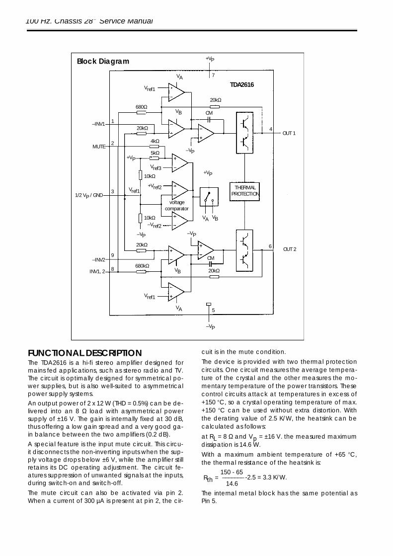
100 Hz. Chassis 28” Service Manual
FUNCTIONAL DESCRIPTIONThe TDA2616 is a hi-fi stereo amplifier designed formains fed applications, such as stereo radio and TV.The circuit is optimally designed for symmetrical po-wer supplies, but is also well-suited to asymmetricalpower supply systems.An output power of 2 x 12 W (THD = 0.5%) can be de-livered into an 8 Ω load with asymmetrical powersupply of ±16 V. The gain is internally fixed at 30 dB,thus offering a low gain spread and a very good ga-in balance between the two amplifiers (0.2 dB).A special feature is the input mute circuit. This circu-it disconnects the non-inverting inputs when the sup-ply voltage drops below ±6 V, while the amplifier stillretains its DC operating adjustment. The circuit fe-atures suppression of unwanted signals at the inputs,during switch-on and switch-off.The mute circuit can also be activated via pin 2.When a current of 300 µA is present at pin 2, the cir-
cuit is in the mute condition.The device is provided with two thermal protectioncircuits. One circuit measures the average tempera-ture of the crystal and the other measures the mo-mentary temperature of the power transistors. Thesecontrol circuits attack at temperatures in excess of+150 oC, so a crystal operating temperature of max.+150 oC can be used without extra distortion. Withthe derating value of 2.5 K/W, the heatsink can becalculated as follows:at RL = 8 Ω and Vp = ±16 V. the measured maximumdissipation is 14.6 W.With a maximum ambient temperature of +65 oC,the thermal resistance of the heatsink is:
Rth =150 - 65
-2.5 = 3.3 K/W._______14.6
The internal metal block has the same potential asPin 5.
–INV1
Vref1
VA
VB
–VP
+VP
THERMALPROTECTION
VA VB
7
4
680Ω
20kΩ
20kΩ
CM
4kΩ
5kΩ
10kΩ
10kΩ
+VP
MUTE
1/2 VP / GND
–INV2
INV1, 2
OUT 2
OUT 1
TDA2616
Vref3
Vref1
–Vref2
+Vref2
voltagecomparator
+VP
–VP –VP
CM
20kΩ
20kΩ680kΩ
1
2
3
9
8
5
6
Vref1
VA
–VP
VB
Block Diagram
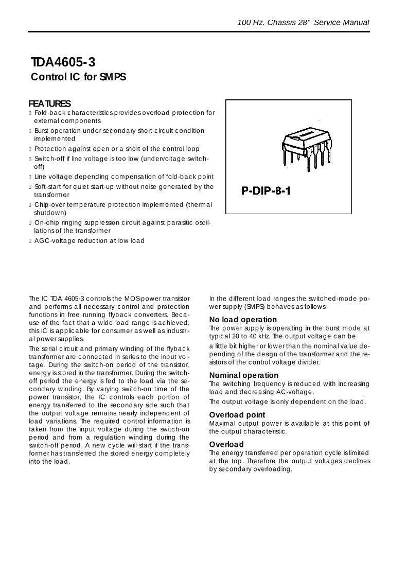
100 Hz. Chassis 28” Service Manual
FEATURESu Fold-back characteristics provides overload protection for
external componentsu Burst operation under secondary short-circuit condition
implementedu Protection against open or a short of the control loopu Switch-off if line voltage is too low (undervoltage switch-
off)u Line voltage depending compensation of fold-back pointu Soft-start for quiet start-up without noise generated by the
transformeru Chip-over temperature protection implemented (thermal
shutdown)u On-chip ringing suppression circuit against parasitic oscil-
lations of the transformeru AGC-voltage reduction at low load
TDA4605-3Control IC for SMPS
The IC TDA 4605-3 controls the MOS-power transistorand performs all necessary control and protectionfunctions in free running flyback converters. Beca-use of the fact that a wide load range is achieved,this IC is applicable for consumer as well as industri-al power supplies.The serial circuit and primary winding of the flybacktransformer are connected in series to the input vol-tage. During the switch-on period of the transistor,energy is stored in the transformer. During the switch-off period the energy is fed to the load via the se-condary winding. By varying switch-on time of thepower transistor, the IC controls each portion ofenergy transferred to the secondary side such thatthe output voltage remains nearly independent ofload variations. The required control information istaken from the input voltage during the switch-onperiod and from a regulation winding during theswitch-off period. A new cycle will start if the trans-former has transferred the stored energy completelyinto the load.
In the different load ranges the switched-mode po-wer supply (SMPS) behaves as follows:
No load operationThe power supply is operating in the burst mode attypical 20 to 40 kHz. The output voltage can bea little bit higher or lower than the nominal value de-pending of the design of the transformer and the re-sistors of the control voltage divider.
Nominal operationThe switching frequency is reduced with increasingload and decreasing AC-voltage.The output voltage is only dependent on the load.
Overload pointMaximal output power is available at this point ofthe output characteristic.
OverloadThe energy transferred per operation cycle is limitedat the top. Therefore the output voltages declinesby secondary overloading.
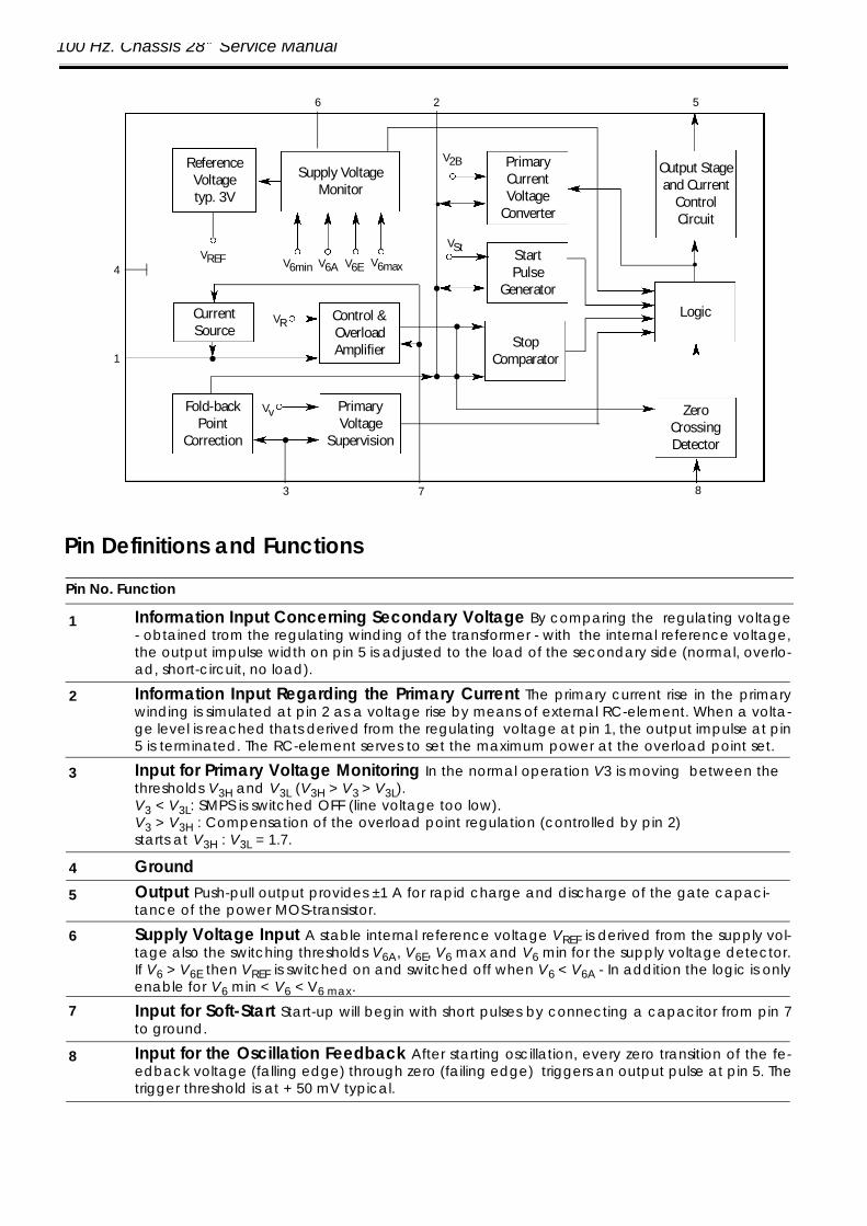
100 Hz. Chassis 28” Service Manual
ReferenceVoltage typ. 3V
PrimaryVoltage
Supervision
Control &OverloadAmplifier
CurrentSource
PrimaryCurrentVoltage
Converter
Output Stageand Current
ControlCircuit
Logic
ZeroCrossingDetector
Supply VoltageMonitor
Fold-backPoint
Correction
Start Pulse
Generator
StopComparator
•
•
•
•
•
•
•
VREF V6min V6maxV6A
VR
Vv
3 7 8
V2B
VStV6E
526
4
1
Information Input Concerning Secondary Voltage By comparing the regulating voltage- obtained trom the regulating winding of the transformer - with the internal reference voltage,the output impulse width on pin 5 is adjusted to the load of the secondary side (normal, overlo-ad, short-circuit, no load).
Information Input Regarding the Primary Current The primary current rise in the primarywinding is simulated at pin 2 as a voltage rise by means of external RC-element. When a volta-ge level is reached thats derived from the regulating voltage at pin 1, the output impulse at pin5 is terminated. The RC-element serves to set the maximum power at the overload point set.
Input for Primary Voltage Monitoring In the normal operation V3 is moving between thethresholds V3H and V3L (V3H > V3 > V3L).V3 < V3L: SMPS is switched OFF (line voltage too low).V3 > V3H : Compensation of the overload point regulation (controlled by pin 2) starts at V3H : V3L = 1.7.
GroundOutput Push-pull output provides ±1 A for rapid charge and discharge of the gate capaci-tance of the power MOS-transistor.
Supply Voltage Input A stable internal reference voltage VREF is derived from the supply vol-tage also the switching thresholds V6A, V6E, V6 max and V6 min for the supply voltage detector.If V6 > V6E then VREF is switched on and switched off when V6 < V6A - In addition the logic is onlyenable for V6 min < V6 < V6 max.
Input for Soft-Start Start-up will begin with short pulses by connecting a capacitor from pin 7to ground.
Input for the Oscillation Feedback After starting oscillation, every zero transition of the fe-edback voltage (falling edge) through zero (failing edge) triggers an output pulse at pin 5. Thetrigger threshold is at + 50 mV typical.
Pin Definitions and Functions
Pin No. Function
1
2
3
4
5
6
7
8
•
•
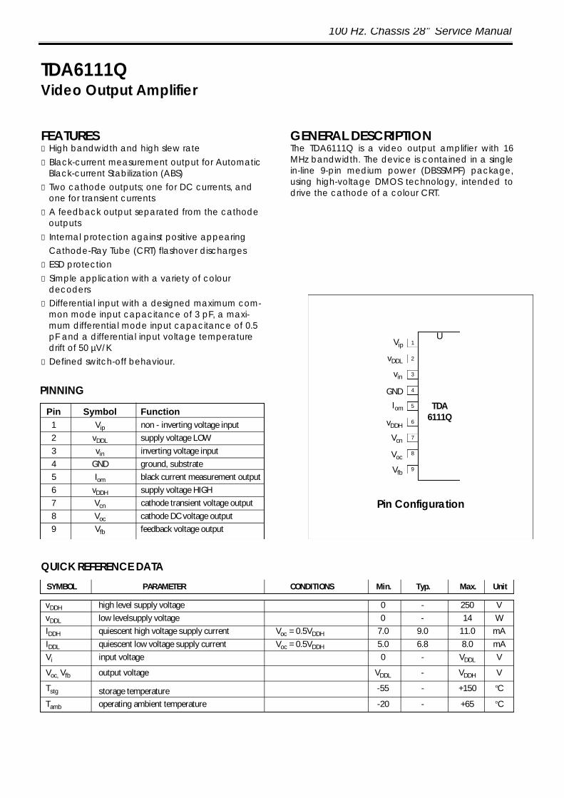
100 Hz. Chassis 28” Service Manual
FEATURESu High bandwidth and high slew rateu Black-current measurement output for Automatic
Black-current Stabilization (ABS)u Two cathode outputs; one for DC currents, and
one for transient currentsu A feedback output separated from the cathode
outputsu Internal protection against positive appearing
Cathode-Ray Tube (CRT) flashover dischargesu ESD protectionu Simple application with a variety of colour
decodersu Differential input with a designed maximum com-
mon mode input capacitance of 3 pF, a maxi-mum differential mode input capacitance of 0.5pF and a differential input voltage temperaturedrift of 50 µV/K
u Defined switch-off behaviour.
GENERAL DESCRIPTIONThe TDA6111Q is a video output amplifier with 16MHz bandwidth. The device is contained in a singlein-line 9-pin medium power (DBSSMPF) package,using high-voltage DMOS technology, intended todrive the cathode of a colour CRT.
TDA6111QVideo Output Amplifier
QUICK REFERENCE DATA
vDDH high level supply voltage 0 - 250 VvDDL low levelsupply voltage 0 - 14 WIDDH quiescent high voltage supply current Voc = 0.5VDDH 7.0 9.0 11.0 mAIDDL quiescent low voltage supply current Voc = 0.5VDDH 5.0 6.8 8.0 mAVi input voltage 0 - VDDL V
Voc, Vfb output voltage VDDL - VDDH V
Tstg storage temperature -55 - +150 oC
Tamb operating ambient temperature -20 - +65 oC
SYMBOL PARAMETER CONDITIONS Min. Typ. Max. Unit
Pin Symbol Function1 Vip non - inverting voltage input2 vDDL supply voltage LOW3 vin inverting voltage input4 GND ground, substrate5 Iom black current measurement output6 vDDH supply voltage HIGH7 Vcn cathode transient voltage output8 Voc cathode DC voltage output9 Vfb feedback voltage output
PINNING
1
2
3
4
5
6
7
Vip
vDDL
vin
GND
Iom
vDDH
Vcn
U
8Voc
9Vfb
TDA6111Q
Pin Configuration
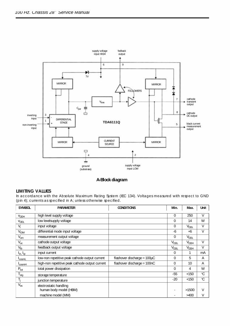
100 Hz. Chassis 28” Service Manual
LIMITING VALUESIn accordance with the Absolute Maximum Rating System (IEC 134). Voltages measured with respect to GND(pin 4); currents as specified in A; unless otherwise specified.
vDDH high level supply voltage 0 250 VvDDL low levelsupply voltage 0 14 WVi input voltage 0 VDDL VVIDM differential mode input voltage -6 +6 VVom measurement output voltage 0 VDDL
Voc cathode output voltage VDDL VDDH VVfb feedback output voltage VDDL VDDH VIin, Iip input current 0 1 mAIcosmL low-non repetitive peak cathode output current flashover discharge = 100µC 0 5 AIcosmH high-non repetitive peak cathode output current flashover discharge = 100nC 0 10 APtot total power dissipation 0 4 WTstg storage temperature -55 +150 oCTj junction temperature -20 +150 oCVes electrostatic handling
human body model (HBM) - >1500 Vmachine model (MM) - >400 V
SYMBOL PARAMETER CONDITIONS Min. Max. Unit
A-Block diagram
supply voltageinput HIGH
fedbackoutput
6 9
7V
MIRROR
FOLLOWERS
Vbias
TDA6111Q
cathodetransientoutput
cathodeDC output
black currentmeasurementoutput
CURRENTSOURCE
MIRROR
5
8
7
MIRROR
Cpar
MIRROR
DIFFERENTIALSTAGE
-
+
3
1
ground(substrate)
4 2
supply voltageinput LOW
invertinginput
non-invertinginput
100 Hz. Chassis 28” Service Manual
Cathode outputThe cathode output is protected against peak cur-rents (caused by positive voltage peaks during high-resistance flash) of 5 A maximum with a charge con-tent of 100 µC.The cathode is also protected against peak currents(caused by positive voltage peaks during low-resis-tance flash) of 10 A maximum with a charge con-tent of 100 nC.
Flashover protectionThe TDA6111Q incorporates protection diodes aga-inst CRT flashover discharges that clamp the catho-de output pin to the VDDH pin. The DC supply volta-ge at the VDDH Pin has to be within the operatingrange of 180 to 210 V to ensure that the AbsoluteMaximum Rating for VDDH of 250 V will not be exce-eded during flashover. To limit the diode current, anexternal 680 R carbon high-voltage resistor in serieswith the cathode output and a 2 kV spark gap areneeded (for this resistor-value, the CRT has to beconnected to the main PCB). This addition producesan increase in the rise and fall times of approxima-tely 5 ns and a decrease in the overshoot of appro-ximately 4%.
VDDH to GND must be decoupled:1. With a capacitor >20 nF with good HF beha
viour (e.g. foil). This capacitance must be placed as close as possible to pins 6 and 4, but definitely within 5 mm.
2. With a capacitor >10 CIF on the picture tubebase print (common for three output stages).
VDDL to GND must be decoupled:1. With a capacitor >20 nF with good HF beha-
viour (e.g. ceramic). This capacitance mustbe placed as close as possible to pins 2 and4, but definitely within 10 mm.
Switch-off behaviourThe switch-off behaviour of the TDA6111Q is defined:when the bias current becomes zero, at VDDL (pin 2)lower than approximately 5 V, all the output pins(pins 7, 8 and 9) will be high.
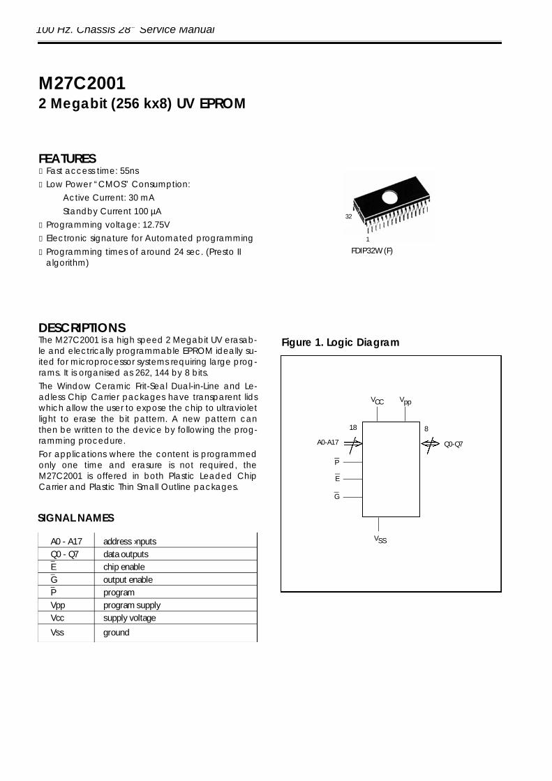
100 Hz. Chassis 28” Service Manual
M27C20012 Megabit (256 kx8) UV EPROM
FEATURESu Fast access time: 55nsu Low Power “CMOS” Consumption:
Active Current: 30 mAStandby Current 100 µA
u Programming voltage: 12.75Vu Electronic signature for Automated programmingu Programming times of around 24 sec. (Presto II
algorithm)
DESCRIPTIONSThe M27C2001 is a high speed 2 Megabit UV erasab-le and electrically programmable EPROM ideally su-ited for microprocessor systems requiring large prog-rams. It is organised as 262, 144 by 8 bits.The Window Ceramic Frit-Seal Dual-in-Line and Le-adless Chip Carrier packages have transparent lidswhich allow the user to expose the chip to ultravioletlight to erase the bit pattern. A new pattern canthen be written to the device by following the prog-ramming procedure.For applications where the content is programmedonly one time and erasure is not required, theM27C2001 is offered in both Plastic Leaded ChipCarrier and Plastic Thin Small Outline packages.
A0 - A17 address ›nputsQ0 - Q7 data outputsE chip enableG output enableP programVpp program supplyVcc supply voltage
Vss ground
SIGNAL NAMES
Figure 1. Logic Diagram
VCC
VSS
A0-A17
P
18 8
Q0-Q7
E
G
Vpp
FDIP32W (F)
32
1
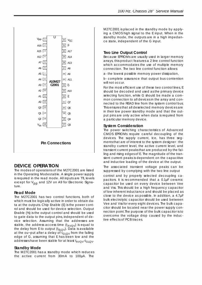
100 Hz. Chassis 28” Service Manual
DEVICE OPERATIONThe modes of operations of the M27C2001 are listedin the Operating Modes table. A single power supplyis required in the read mode. All inputs are TTL levelsexcept for Vpp and 12V on A9 for Electronic Signa-ture.
Read ModeThe M27C2001 has two control functions, both ofwhich must be logically active in order to obtain da-ta at the outputs. Chip Enable (E) is the power cont-rol and should be used for device selection. OutputEnable (%) is the output control and should be usedto gate data to the output pins, independent of de-vice selection. Assuming that the addresses arestable, the address access time (tAVQV) is equal tothe delay from E to output (tELQV). Data is availableat the ou~put after a delay of tGLQV from the fallingedge of G, assuming that E has been low and theaddresses have been stable for at least tAVQV-tGLQV.
Standby ModeThe M27C2001 has a standby mode which reducesthe active current from 30mA to 100µA. The
M27C2001 is placed in the standby mode by apply-ing a CMOS high signal to the E input. When in thestandby mode, the outputs are in a high impedan-ce state, independent of the G input.
Two Line Output ControlBecause EPROMs are usually used in larger memoryarrays, this product features a 2 line control functionwhich accommodates the use of multiple memoryconnection. The two line control function allows:a- the lowest possible memory power dissipation,b- complete assurance that output bus contentionwill not occur.For the most efficient use of these two control lines, Eshould be decoded and used as the primary deviceselecting function, while G should be made a com-mon connection to all devices in the array and con-nected to the READ line from the system control bus.This ensures that all deselected memory devices arein their low power standby mode and that the out-put pins are only active when data is required froma particular memory device.
System ConsiderationThe power switching characteristics of AdvancedCMOS EPROMs require careful decoupling of thedevices. The supply current, Ice, has three seg-ments that are of interest to the system designer : thestandby current level, the active current level, andtransient current peaks that are produced by the fal-ling and rising edges of E. The magnitude of the tran-sient current peaks is dependent on the capacitiveand inductive loading of the device at the output.The associated transient voltage peaks can besuppressed by complying with the two line outputcontrol and by properly selected decoupling ca-pacitors. It is recommended that a 0.1µF ceramiccapacitor be used on every device between Veeand Vss. This should be a high frequency capacitorof low inherent inductance and should be placed asclose to the device as possible. In addition, a 4.7µFbulk electrolytic capacitor should be used betweenVee and Vss for every eight devices. The bulk capa-citor should be located near the power supply con-nection point.The purpose of the bulk capacitor is toovercome the voltage drop caused by the induc-tive effects of PCB traces.
1
2
3
4
5
6
7
28
27
26
25
24
23
22
VPP
A16
A15
A12
A7
A6
A5
U
A13
A8
A9
A11
G
A10
E
8
21
A4
Q7
9
20
A3
Q6
10
19
A2
Q5
11
18
A1
Q4
12
17
A0
Q3
13
32
Q0
VCC
14
31
Q1
P
15
30
Q2
A17
16
29
Vss
A14
A10M27C2001
Pin Connections
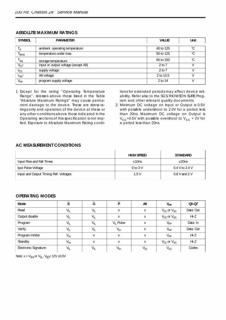
100 Hz. Chassis 28” Service Manual
ABSOLUTE MAXIMUM RATINGS
TA ambient operating temperature 40 to 125 oCTBIAS temperature under b›as 50 to 125 oC
Tstg storage temperature 65 to 150 oCVIO
(2) input or output voltage (except A9) 2 to 7 VvCC supply voltage 2 to 7 VvA9
(2) A9 voltage 2 to 13.5 VVPP program supply voltage 2 to 14 V
SYMBOL PARAMETER VALUE Unit
1 Except for the rating “Operating TemperatureRange”, stresses above those listed in the Table"Absolute Maximum Ratings'” may cause perma-nent damage to the device. These are stress ra-tings only and operation of the device at these orany other conditions above those indicated in theOperating sections of this specification is not imp-lied. Exposure to Absolute Maximum Rating condi-
tions for extended periods may affect device reli-ability. Refer also to the SGS-THOMSON SURE Prog-ram and other relevant quality documents.
2. Minimum DC voltage on Input or Output is 0.5Vwith possible undershoot to 2.0V for a period lessthan 20ns. Maximum DC voltage on Output isVcc+0.5V with possible overshoot to Vcc + 2V fora period less than 20ns.
AC MEASUREMENT CONDITIONS
HIGH SPEED STANDARD
Input Rise and Fall Times ≤10ns ≤20ns
Iput Pulse Voltage 0 to 3 V 0.4 V to 2.4 V
Input and Output Timing Ref. Voltages 1.5 V 0.8 V and 2 V
OPERATING MODES
Mode E G P A9 VPP Q0-Q7
Read VIL VIL x x VCC or VSS Data Out
Output disable VIL VIL x x VCC or VSS Hi-Z
Program VIL VIL VIL Pulse x VPP Data In
Verify VIL VIL VIH x VPP Data Out
Program Inhibit VIH x x x VPP Hi-Z
Standby VIH x x x VCC or VSS Hi-Z
Electronic Signature VIL VIL VIH VID VCC Codes
Note: x = VIH or VIL, VID= 12V ±0.5V
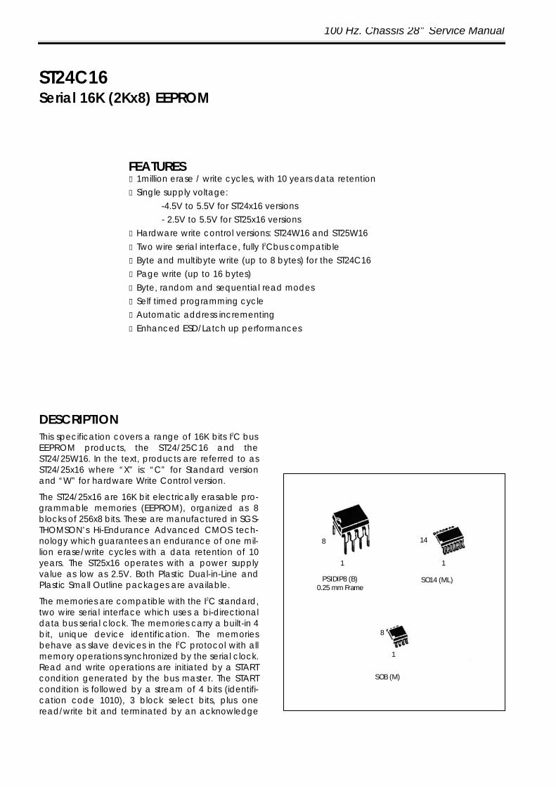
100 Hz. Chassis 28” Service Manual
ST24C16Serial 16K (2Kx8) EEPROM
DESCRIPTIONThis specification covers a range of 16K bits I2C busEEPROM products, the ST24/25C16 and theST24/25W16. In the text, products are referred to asST24/25x16 where “X” is: “C” for Standard versionand “W” for hardware Write Control version.
The ST24/25x16 are 16K bit electrically erasable pro-grammable memories (EEPROM), organized as 8blocks of 256x8 bits. These are manufactured in SGS-THOMSON’s Hi-Endurance Advanced CMOS tech-nology which guarantees an endurance of one mil-lion erase/write cycles with a data retention of 10years. The ST25x16 operates with a power supplyvalue as low as 2.5V. Both Plastic Dual-in-Line andPlastic Small Outline packages are available.
The memories are compatible with the I2C standard,two wire serial interface which uses a bi-directionaldata bus serial clock. The memories carry a built-in 4bit, unique device identification. The memoriesbehave as slave devices in the I2C protocol with allmemory operations synchronized by the serial clock.Read and write operations are initiated by a STARTcondition generated by the bus master. The STARTcondition is followed by a stream of 4 bits (identifi-cation code 1010), 3 block select bits, plus oneread/write bit and terminated by an acknowledge
FEATURESu 1million erase / write cycles, with 10 years data retentionu Single supply voltage:
-4.5V to 5.5V for ST24x16 versions- 2.5V to 5.5V for ST25x16 versions
u Hardware write control versions: ST24W16 and ST25W16u Two wire serial interface, fully I2Cbus compatibleu Byte and multibyte write (up to 8 bytes) for the ST24C16u Page write (up to 16 bytes)u Byte, random and sequential read modesu Self timed programming cycleu Automatic address incrementingu Enhanced ESD/Latch up performances
PSIDIP8 (B)0.25 mm Frame
SO14 (ML)
SOB (M)
8
1 1
14
8
1
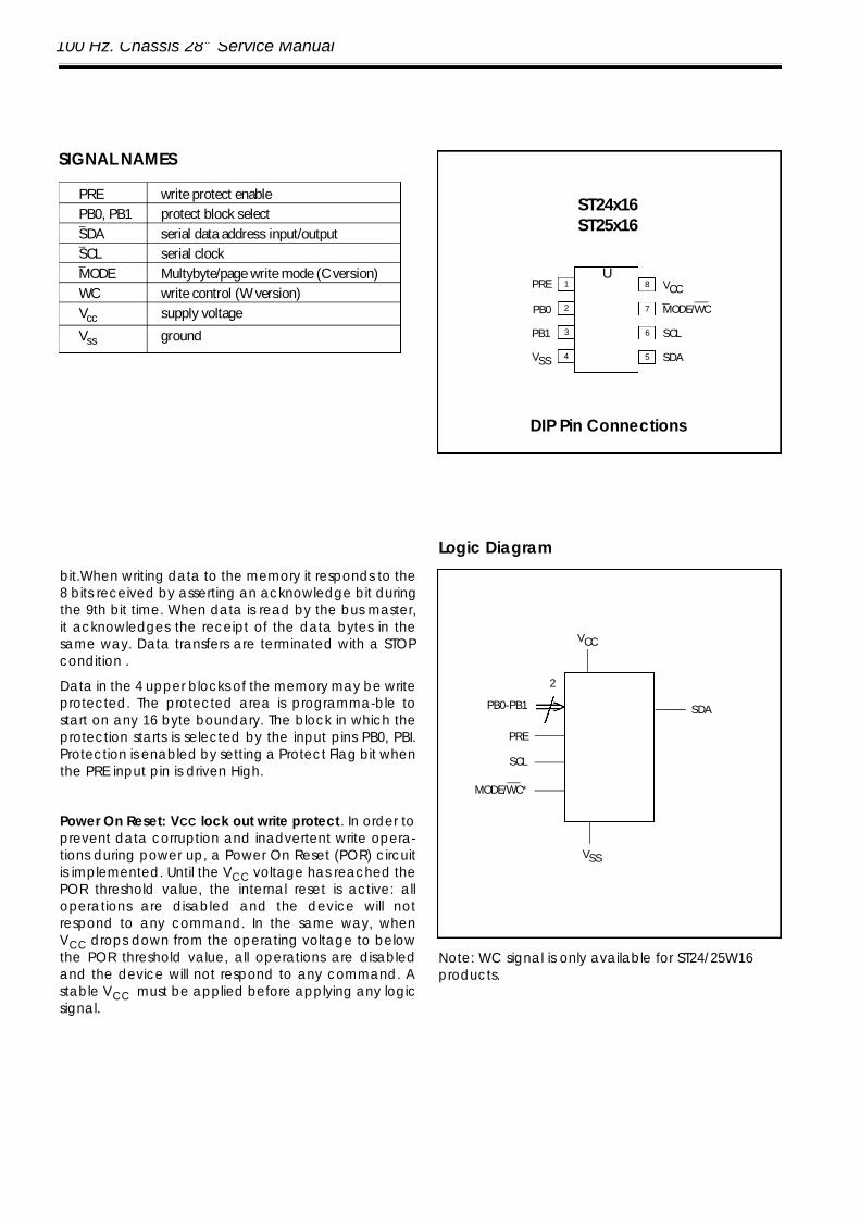
100 Hz. Chassis 28” Service Manual
PRE write protect enablePB0, PB1 protect block selectSDA serial data address input/outputSCL serial clockMODE Multybyte/page write mode (C version)WC write control (W version)Vcc supply voltage
Vss ground
SIGNAL NAMES
1
2
3
4
PRE
PB0
PB1
VSS
VCC
SDA
VSS
PB0-PB1
PRE
2
SCL
MODE/WC*
U8 VCC
7 MODE/WC
6 SCL
5 SDA
ST24x16ST25x16
DIP Pin Connections
Logic Diagram
Note: WC signal is only available for ST24/25W16products.
bit.When writing data to the memory it responds to the8 bits received by asserting an acknowledge bit duringthe 9th bit time. When data is read by the bus master,it acknowledges the receipt of the data bytes in thesame way. Data transfers are terminated with a STOPcondition .
Data in the 4 upper blocks of the memory may be writeprotected. The protected area is programma-ble tostart on any 16 byte boundary. The block in which theprotection starts is selected by the input pins PB0, PBI.Protection is enabled by setting a Protect Flag bit whenthe PRE input pin is driven High.
Power On Reset: VCC lock out write protect . In order toprevent data corruption and inadvertent write opera-tions during power up, a Power On Reset (POR) circuitis implemented. Until the VCC voltage has reached thePOR threshold value, the internal reset is active: alloperations are disabled and the device will notrespond to any command. In the same way, whenVCC drops down from the operating voltage to belowthe POR threshold value, all operations are disabledand the device will not respond to any command. Astable VCC must be applied before applying any logicsignal.
100 Hz. Chassis 28” Service Manual
SAA7710TDolby Pro Logic Surround; Dolby 3 stereo; Incredible Sound
GENERAL DESCRIPTIONThis specification describes the 104 ROM-code ver-sion of the SAA7710T chip. The SAA7710T chip is ahigh quality audio-performance digital add-on pro-cessor for digital sound systems. It provides all the ne-cessary features for complete Dolby Pro Logic surro-und sound on chip.In addition to the Dolby Pro Logic surround function,this device also incorporates a 3-band parametricequalizer, a 5-band parametric equalizer, a tonecontrol section and a volume control. Instead ofDolby Pro Logic surround, the Hall/matrix surroundand Incredible sound functions can be used toget-her with the equalizer or tone control.
FEATURESu Two stereo I2S-bus digital input channelsu Three stereo I2S-bus digital output channelsu I2C-bus mode controlu Up to 45 ms on-chip delay-line (fs = 44.1 kHz)u Optional clock divider for crystal oscillatoru Package: SO32Lu Operating supply voltage range: 4.5 to 5.5 V.
Functionsu 4-channel active surround, 20 Hz to 20 kHz
(maximum i/2fs)u Adaptive matrixu 7 kHz low-pass filtersu Adjustable delay for surround channelu Modified Dolby B noise reductionu Noise sequenceru Variable output matrixu Sub wooferu Centre mode control: on/off, normal, phantom, wideu Output volume controlu Automatic balance and master level control with DC-
offset filteru Hallimatrix surround sound functionsu Incredible sound functionsu 8-band parametric equalizer on main channels left,
centre, right (fs = 44.1 kHz)u 5-band parametric equalizer on main channels left,
centre, right (fs = 32 kHz)u Tone control (bass/treble) on all four output channels
(fs = 44.1 kHz).
QUICK REFERENCE DATA
vDD DC supply voltage -0.5 +6.5 V∆vDD voltage difference between two V DDx pins - 550 mVvi Maximum input voltage -0.5 VDD+0.5 VIDD DC supply current - 50 mAIss DC supply current - 50 mATamb ambient operating temperature -40 +85 oCTstg storage temperature range -65 +150 oC
SYMBOL PARAMETER Min. Max. Unit
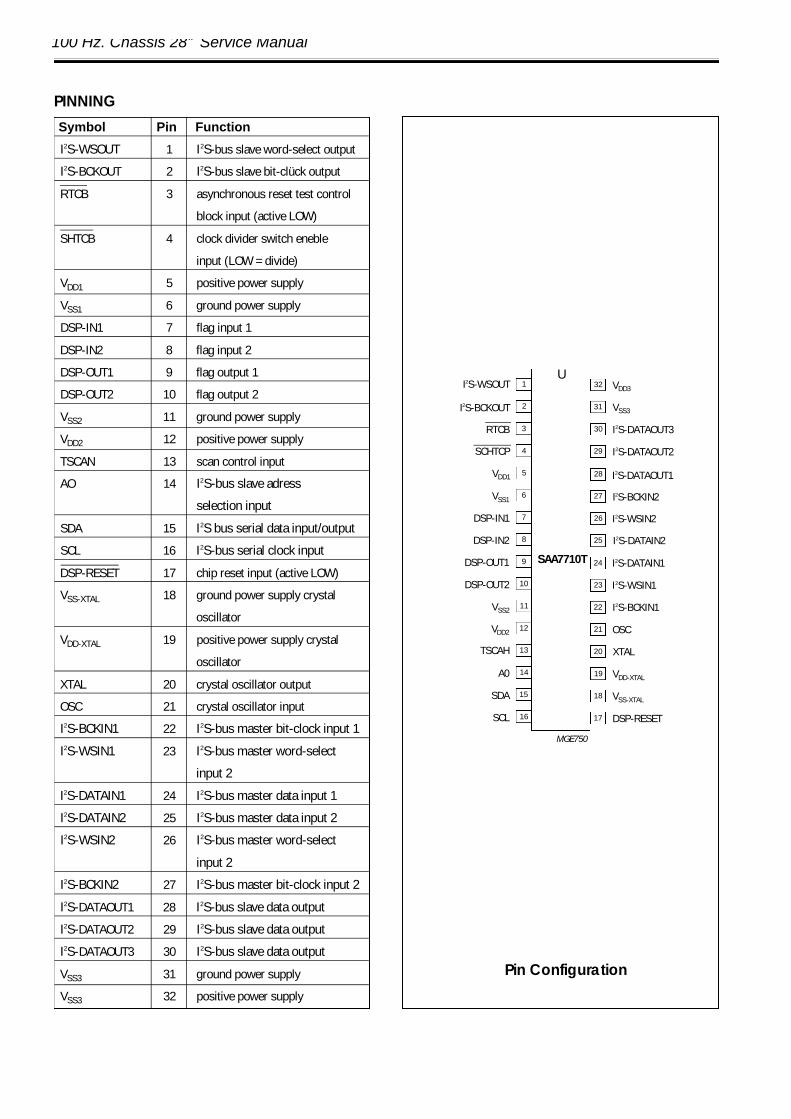
100 Hz. Chassis 28” Service Manual
1
2
3
4
5
6
7
28
27
26
25
24
23
22
I2S-WSOUT
I2S-BCKOUT
RTCB
SCHTCP
VDD1
VSS1
DSP-IN1
U
I2S-DATAOUT1
I2S-BCKIN2
I2S-WSIN2
I2S-DATAIN2
I2S-DATAIN1
I2S-WSIN1
I2S-BCKIN1
8
21
DSP-IN2
OSC
9
20
DSP-OUT1
XTAL
10
19
DSP-OUT2
VDD-XTAL
11
18
VSS2
VSS-XTAL
12
17
VDD2
DSP-RESET
13
32
TSCAH
VDD3
14
31
A0
VSS3
15
30
SDA
I2S-DATAOUT3
16
29
SCL
I2S-DATAOUT2
SAA7710T
Pin Configuration
MGE750
Symbol Pin Function
I2S-WSOUT 1 I2S-bus slave word-select output
I2S-BCKOUT 2 I2S-bus slave bit-clück output
RTCB 3 asynchronous reset test control
block input (active LOW)
SHTCB 4 clock divider switch eneble
input (LOW = divide)
VDD1 5 positive power supply
VSS1 6 ground power supply
DSP-IN1 7 flag input 1
DSP-IN2 8 flag input 2
DSP-OUT1 9 flag output 1
DSP-OUT2 10 flag output 2
VSS2 11 ground power supply
VDD2 12 positive power supply
TSCAN 13 scan control input
AO 14 I2S-bus slave adress
selection input
SDA 15 I2S bus serial data input/output
SCL 16 I2S-bus serial clock input
DSP-RESET 17 chip reset input (active LOW)
VSS-XTAL 18 ground power supply crystal
oscillator
VDD-XTAL 19 positive power supply crystal
oscillator
XTAL 20 crystal oscillator output
OSC 21 crystal oscillator input
I2S-BCKIN1 22 I2S-bus master bit-clock input 1
I2S-WSIN1 23 I2S-bus master word-select
input 2
I2S-DATAIN1 24 I2S-bus master data input 1
I2S-DATAIN2 25 I2S-bus master data input 2
I2S-WSIN2 26 I2S-bus master word-select
input 2
I2S-BCKIN2 27 I2S-bus master bit-clock input 2
I2S-DATAOUT1 28 I2S-bus slave data output
I2S-DATAOUT2 29 I2S-bus slave data output
I2S-DATAOUT3 30 I2S-bus slave data output
VSS3 31 ground power supply
VSS3 32 positive power supply
PINNING
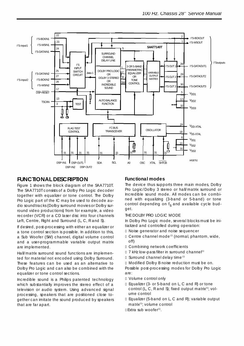
100 Hz. Chassis 28” Service Manual
FUNCTIONAL DESCRIPTIONFigure 1 shows the block diagram of the SAA7710T.The SAA7710T consists of a Dolby Pro Logic decodertogether with equalizer or tone control. The DolbyPro Logic part of the IC may be used to decode au-dio soundtracks (Dolby surround movies or Dolby sur-round video productions) from for example, a videorecorder (VCR) or a CD laser disc into four channelsLeft, Centre, Right and Surround (L, C, R and S).If desired, post-processing with either an equalizer ora tone control section is possible. In addition to this,a Sub Woofer (SW) channel, digital volume controland a user-programmable variable output matrixare implemented.Hall/matrix surround sound functions are implemen-ted for material not encoded using Dolby Surround.These features can be used as an alternative toDolby Pro Logic and can also be combined with theequalizer or tone control sections.Incredible sound is a Philips patented technologywhich substantially improves the stereo effect of atelevision or audio system. Using advanced signalprocessing, speakers that are positioned close to-gether can imitate the sound produced by speakersthat are far apart.
Functional modesThe device thus supports three main modes, DolbyPro Logic/Dolby 3 stereo or hall/matrix surround orIncredible sound mode. All modes can be combi-ned with equalizing (3-band or 5-band) or tonecontrol depending on fs and available cycle bud-get.
THE DOLBY PRO LOGIC MODEIn Dolby Pro Logic mode, several blocks must be ini-tialized and controlled during operation:u Noise generator and noise sequenceru Centre channel mode(1) (normal, phantom, wide,
off)u Combining network coefficientsu 7 kHz low-pass filter in surround channel(1)
u Surround channel delay time (1)
u Modified Dolby B noise reduction must be on.Possible post-processing modes for Dolby Pro Logicare:u Volume control onlyu Equalizer (3- or 5-band on L, C and R) or tone
control (L, C, R and S); fixed output matrix(1); vol-ume control
u Equalizer (5-band on L, C and R); variable outputmatrix(1); volume control
u Extra sub woofer(1).
I2S-BCKIN1
I2S-WSIN1
I2S-DATAIN1
I2S-input1
I2S-DATAIN2
I2S-BCKIN2
I2S-WSIN2
DSP-RESET
TSCAN
I2S-input2
22
23
data 1
S
L
C
R
SW
24
25
27
26
17
13
3
FLAG TESTCONTROL
I2C BUSTRANSCEIVER OSCILLATOR
TEST
I2SINPUT
SWITCHCIRCUIT
SURROUNDCHANNEL
DELAY LINE
DOLBY PRO LOGICOR
DOLBY 3 STEREOOR
INCREDIBLESOUND
AUTO BALANCEFUNCTION
3 OR 5-BANDPARAMETRICEQUALIZER
ORTONE
CONTROL
VARIABLEOUTPUTMATRIX
I2S OUT 1
I2S OUT 2
I2S OUT 3
28
2
1
29
30
12
32
19
18
6
11
31
5
31313131313131313131
DSP-IN1
DSP-IN2
DSP-OUT1DSP-OUT2
SDA SCL A0 OSC XTAL SHTCB
I2S-BCKOUT
I2S-WSOUT
I2S-DATAOUT1
VDD1
I2S-DATAOUT2
I2S-DATAOUT3
VDD2
VDD3
VDD-XTAL
VSS-XTAL
VSS1
VSS2
VSS3
MGE751
I2Soutputs
SAA77140T
100 Hz. Chassis 28” Service Manual
THE DOLBY 3 STEREO MODEin Dolby 3 stereo mode, several blocks must be initi-alized and controlled during operation:u Nojise generator and noise sequenceru Centre channel model (1) (normal, phantom, wide
and off)u Combining network coefficients.
THE HALL/MATRIX SURROUND MODEIn hall/matrix surround mode, the blocks listed belowmust be initialized and controlled during operation:u Input balance controlu Hall or matrix surround Mode settingu All-pass and filter transfer characteristic(1)
u 7 kHz low-pass filter in surround channel(1)
u Surround channel delay (1)
Possible post-processing modes for hall/matrix surro-und are as above:u Volume control onlyu Equalizer (3- or 5-band on L, C and R) or tone
control (L, C, R and S); fixed output matrix(1); volu-me control
u Equalizer (5-band on L,C,R): variable output mat-rix(1) volume control
u Extra sub woofer(1)
THE INCREDIBLE SOUND MODEIn the Incredible sound mode the blocks listed belowmust be initialized and controlled during operation:u Incredible sound coefficientsu Combining network coefficients.Possible post-processing modes for incredible soundare as follows:u Volume control onlyu Equalizer (5-band on L and R) or tone control (L
and R); variable output matrix(1), volume controlu Extra sub-woofer(1).
ADDITIONAL INFORMATIONThe possible modes of operation are discussed inmore detail in the "SAA 7710T Dolby Pro Logic Prog-ramming Guide, Application Note AN95063”: This al-so includes which features are available for a givensystem clock frequency and sample frequency andthe possible input configurations.
Clock circuit and oscillatorThe chip has an on board crystal clock oscillator. Theblock schematic of this Pierce oscillator is shown inFigs 3 and 4. The active element needed to com-pensate for the loss resistance of the crystal is theamplifier Gm.This amplifier is placed between the XTAL (output)pin and the OSC (sense) pin. The gain of the oscilla-tor is internally controlled by the automatic gain
control. This prevents too much power loss in thecrystal. The higher harmonics are then as low as pos-sible. The signals on the OSC and XTAL pin are diffe-rentially amplified.The oscillator has these two modes of operation:The crystal oscillator mode: in this mode a quartzcrystal oscillator is used to generate a clock signalwhich is subsequently divided by 2 to ensure that thefinal clock signal has a 50% duty cycle.The oscillator circuit components Rbias and C1, C2depend on the crystal. In the case of an overtoneoscillator, the ground harmonic is filtered out by L1and C3. Pin SHTCB is held low so that the divided sig-nal is selected. Only a quartz crystal should be usedin this mode.The slave oscillator mode: in this mode the oscillatorcircuit acts as a slave driven by a master systemclock. The clock divider can be switched on or offusing pin SHTCB. When the divider is not used, theduty cycle of the clock will depend on the mastersystem clock duty cycle and the rising and fallingedge times. This places a tolerance of 5% on the 50%duty cycle of the master system clock (see Chapter"AC characteristics").In order to be able to control the phase of the clocksignal during testing the divider is skipped and thesignal is directly fed to the circuit via the multiplexerin the TEST position.
SUPPLY OF THE CRYSTAL OSCILLATORThe power supply connections to the oscillator areseparated from the other supply lines to minimisefeedback from on-chip ground bounce to the oscil-lator circuit. Noise on the power supply affects theAGC operation so the power supply should bedecoupled. The VSS-XTAL pin is used as ground sup-ply and theVDD-XTAL as positive supply.
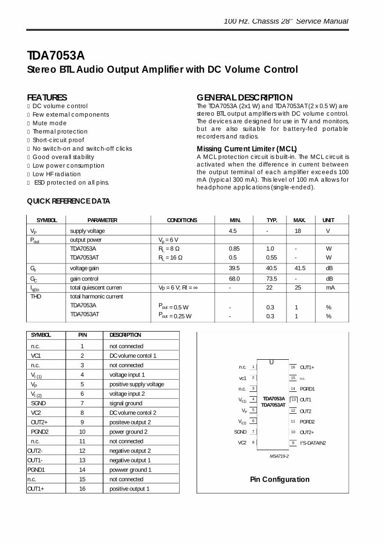
100 Hz. Chassis 28” Service Manual
SYMBOL PARAMETER CONDITIONS MIN. TYP. MAX. UNIT
VP supply voltage 4.5 - 18 VPout output power Vp = 6 V
TDA7053A RL = 8 Ω 0.85 1.0 - WTDA7053AT RL = 16 Ω 0.5 0.55 - W
Gv voltage gain 39.5 40.5 41.5 dB
GC gain control 68.0 73.5 - dBIq(to total quiescent curren Vp = 6 V; Rl = ∞ - 22 25 mATHD total harmonic current
TDA7053A Pout = 0.5 W - 0.3 1 %TDA7053AT Pout = 0.25 W - 0.3 1 %
1
2
3
4
5
6
7
12
11
10
9
n.c.
vc1
n.c.
VI(1)
VP
VI(2)
SGND
U
OUT2
PGRD2
OUT2+
I2S-DATAIN28VC2
16 OUT1+
15 n.c.
14 PGRD1
OUT1TDA7053ATDA7053AT
Pin Configuration
MSA719-2
13
SYMBOL PIN DESCRIPTION
n.c. 1 not connected
VC1 2 DC volume contol 1
n.c. 3 not connected
VI (1) 4 voltage input 1
VP 5 positive supply voltage
VI (2) 6 voltage input 2
SGND 7 signal ground
VC2 8 DC volume contol 2
OUT2+ 9 positeve output 2
PGND2 10 power ground 2
n.c. 11 not connected
OUT2- 12 negative output 2
OUT1- 13 negative output 1
PGND1 14 powwer ground 1
n.c. 15 not connected
OUT1+ 16 positive output 1
QUICK REFERENCE DATA
TDA7053AStereo BTL Audio Output Amplifier with DC Volume Control
FEATURESu DC volume controlu Few external componentsu Mute modeu Thermal protectionu Short-circuit proofu No switch-on and switch-off clicksu Good overall stabilityu Low power consumptionu Low HF radiationu ESD protected on all pins.
GENERAL DESCRIPTIONThe TDA7053A (2x1 W) and TDA7053AT (2 x 0.5 W) arestereo BTL output amplifiers with DC volume control.The devices are designed for use in TV and monitors,but are also suitable for battery-fed portablerecorders and radios.
Missing Current Limiter (MCL)A MCL protection circuit is built-in. The MCL circuit isactivated when the difference in current betweenthe output terminal of each amplifier exceeds 100mA (typical 300 mA). This level of 100 mA allows forheadphone applications (single-ended).
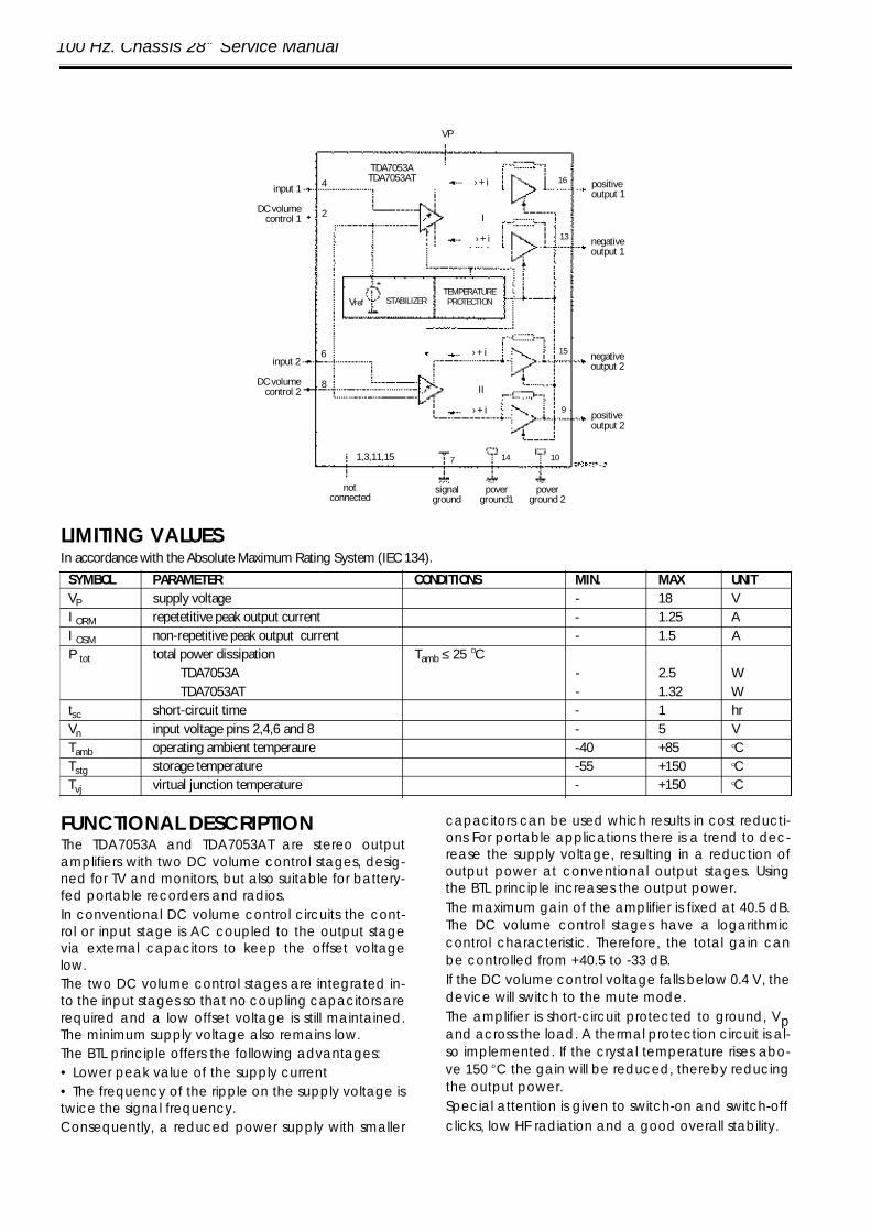
100 Hz. Chassis 28” Service Manual
LIMITING VALUESIn accordance with the Absolute Maximum Rating System (IEC 134).
SYMBOL PARAMETER CONDITIONS MIN. MAX UNITVP supply voltage - 18 VI ORM repetetitive peak output current - 1.25 AI OSM non-repetitive peak output current - 1.5 AP tot total power dissipation Tamb ≤ 25 OC
TDA7053A - 2.5 WTDA7053AT - 1.32 W
tsc short-circuit time - 1 hrVn input voltage pins 2,4,6 and 8 - 5 VTamb operating ambient temperaure -40 +85 OCTstg storage temperature -55 +150 OCTvj virtual junction temperature - +150 OC
FUNCTIONAL DESCRIPTIONThe TDA7053A and TDA7053AT are stereo outputamplifiers with two DC volume control stages, desig-ned for TV and monitors, but also suitable for battery-fed portable recorders and radios.In conventional DC volume control circuits the cont-rol or input stage is AC coupled to the output stagevia external capacitors to keep the offset voltagelow.The two DC volume control stages are integrated in-to the input stages so that no coupling capacitors arerequired and a low offset voltage is still maintained.The minimum supply voltage also remains low.The BTL principle offers the following advantages:• Lower peak value of the supply current• The frequency of the ripple on the supply voltage istwice the signal frequency.Consequently, a reduced power supply with smaller
capacitors can be used which results in cost reducti-ons For portable applications there is a trend to dec-rease the supply voltage, resulting in a reduction ofoutput power at conventional output stages. Usingthe BTL principle increases the output power.The maximum gain of the amplifier is fixed at 40.5 dB.The DC volume control stages have a logarithmiccontrol characteristic. Therefore, the total gain canbe controlled from +40.5 to -33 dB.If the DC volume control voltage falls below 0.4 V, thedevice will switch to the mute mode.The amplifier is short-circuit protected to ground, Vpand across the load. A thermal protection circuit is al-so implemented. If the crystal temperature rises abo-ve 150 oC the gain will be reduced, thereby reducingthe output power.Special attention is given to switch-on and switch-offclicks, low HF radiation and a good overall stability.
input 1
DC volumecontrol 1
4
2
TDA7053ATDA7053AT
VP
› + i
› + i
I
16
13
positiveoutput 1
negativeoutput 1
negativeoutput 2
positiveoutput 2
signalground
poverground1
poverground 2
notconnected
1,3,11,15 7 1014
› + i
II
9
15› + i
T E M P E R A T U R EP R O T E C T I O NS T A B I L I Z E RVref
input 2
DC volumecontrol 2
6
8
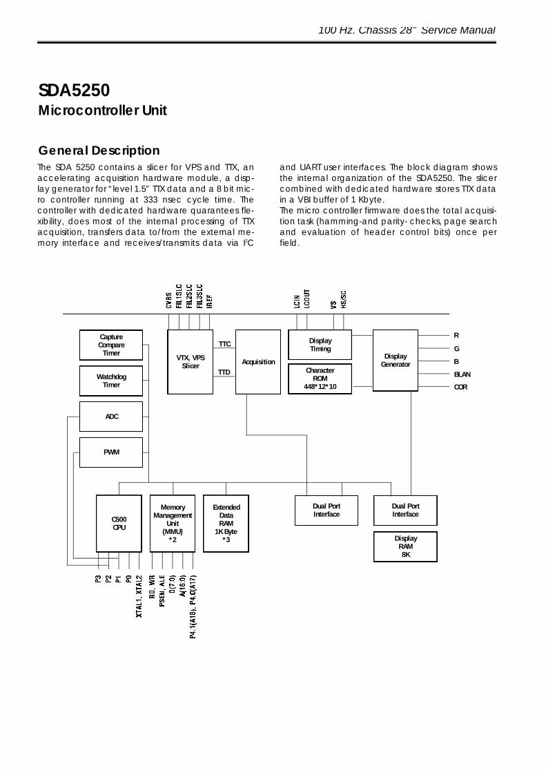
100 Hz. Chassis 28” Service Manual
The SDA 5250 contains a slicer for VPS and TTX, anaccelerating acquisition hardware module, a disp-lay generator for “level 1.5” TTX data and a 8 bit mic-ro controller running at 333 nsec cycle time. Thecontroller with dedicated hardware quarantees fle-xibility, does most of the internal processing of TTXacquisition, transfers data to/from the external me-mory interface and receives/transmits data via I2C
and UART user interfaces. The block diagram showsthe internal organization of the SDA5250. The slicercombined with dedicated hardware stores TTX datain a VBI buffer of 1 Kbyte. The micro controller firmware does the total acquisi-tion task (hamming-and parity- checks, page searchand evaluation of header control bits) once perfield.
CaptureCompare
Timer
WatchdogTimer
Dual PortInterface
Dual PortInterface
DisplayRAM8K
C500CPU
MemoryManagement
Unit(MMU)
*2
ExtendedDataRAM
1K Byte*3
VTX, VPSSlicer Acquisition
DisplayTiming
CharacterROM
448*12*10
TTC
TTD
R
G
B
BLAN
COR
ADC
PWM
DisplayGenerator
SDA5250Microcontroller Unit
General Description
100 Hz. Chassis 28” Service Manual
Symbol Pin number Function Pin voltage
SCL 48 I2C-Bus clock line (SCL) 5V/VppSDA 49 I2C-Bus data line (SDA) 5V/VppEXT2 50 EXT2 -RSTMSP 51 Reset Msp 5VKYB4 52 Keyboard scan line input / output -KYB3 53 Keyboard scan line input / output -KYB2 54 Keyboard scan line input / output -KYB1 55 Keyboard scan line input / output -VOL 84 Volume control output 0-5VCOLOR 83 Color control output 0-5VBRI 82 Brightness control output 0-5VCON 81 Contrast control output 0-5VHUE 80 Hue control output 0-5VSTD 79 Standard select input 5VL/L’ 78 L / l’ output -VTUNE 77 Tuning voltage 0-5VAFC 61 Analogue AFC sense input -STATUS-AV 60 Status AV input ( 1or 2 AV) -AGC 59 Automatic Gain Control Output -AVOUT 76 AV select output 0-5VBND2 75 Band switch 2-output 0-5VBND0 74 Band switch 1-output 0-5VIRIN 73 Remote control output 0-5VBND1 72 Band switch 0-output 0-5VMUTE 71 Mute output for sound -OFF / ON 70 Stand-by / On control input / output -NEG / POS 69A0, A1,...A18 29,27,26 Address bus for external memory 5Vpp
24,22,2018,16,1719,25,2114,15,1312,10,9,11
D0, D1,...D7 31,33,35 Data bus for external memory 5Vpp36,34,3230,28
PSEN 23 Program store enable -ALE 8 Address latch enable -XTAL1 4 Input to the inverting oscillator amp. 5VXTAL2 3 Output of the inverting oscillator amp. 5V
Microcontroller Unit
100 Hz. Chassis 28” Service Manual
Symbol Pin number Function Pin voltage
RST 5 Power on reset 5VVdd 2,43 Power supply voltage 5VVss 1,42 Ground 0VRD 7 Read access from external memory -WR 6 6 Write access to external memory -R 37 OSD Red color signal output 4.5VppG 38 OSD Green color signal output 4.5VppB 39 OSD Blue color signal output 4.5VppBLAN 40 OSD fast blanking output 4.5VppCOR 41 Contrast reduction outputHS/SC 46 Horizontal sync input 5Vpp,HFVS 47 Vertical sync input 5Vpp,HFCVBS 68 CVBS input 5VppIREF 67 Reference current for slicer PLLs -VDDA 66 Analog supply voltage for slicer 5VVSSA 62 Analog ground for slicer 0VFIL1SLC 65 PLL loop filter I/O for vps slicing -FIL2SLC 64 PLL loop filter I/O for teletext slicing 0VFIL3SLC 63 PLL loop filter I/O for phase shifting
of VPS teletext data -LCIN 44 LCIN and LCOUT are used to connect
the external display dot clock frequency -LCOUT 45 reference -NC 56,57 Not connected -
VCC 32 Supply voltage 5VVDD 16 Ground 0VA0-A16 12,11,10 Address Bus 0-5
9,8,7,6,54,3,2,2325,26,2728,29
D0-D7 13,14,15 Data Bus 0-5V17,18,1920,21
E 22 Enable 0-5VG 24 Output Enable -VPP 1 Programming Voltage -PGM 31 Programming Pulse -NC 30 Not Connected -
27C010 (27C1001) EPROM
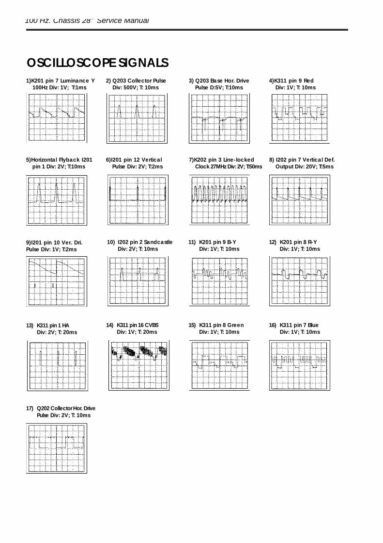
100 Hz. Chassis 28” Service Manual
1)K201 pin 7 Luminance Y 100Hz Div: 1V; T:1ms
5)Horizontal Flyback I201 pin 1 Div: 2V; T:10ms
9)I201 pin 10 Ver. Dri.Pulse Div: 1V; T:2ms
1 3 ) K311 pin 1 HADiv: 2V; T: 20ms
1 4 ) K311 pin 16 CVBSDiv: 1V; T: 20ms
10) I202 pin 2 Sandcastle Div: 2V; T: 10ms
1 1 ) K201 pin 9 B-YDiv: 1V; T: 10ms
12) K201 pin 8 R-YDiv: 1V; T: 10ms
2) Q203 Collector Pulse Div: 500V; T: 10ms
3) Q203 Base Hor. DrivePulse D:5V; T:10ms
4)K311 pin 9 RedDiv: 1V; T: 10ms
1 5 ) K311 pin 8 GreenDiv: 1V; T: 10ms
1 6 ) K311 pin 7 BlueDiv: 1V; T: 10ms
1 7 ) Q202 Collector Hor. Drive P u l s e Div: 2V; T: 10ms
6)I201 pin 12 Vertical Pulse Div: 2V; T:2ms
7)K202 pin 3 Line-locked Clock 27MHz Div: 2V; T:50ms
8) I202 pin 7 Vertical Def. Output Div: 20V; T:5ms
OSCILLOSCOPE SIGNALS