Embed Size (px)
Citation preview
SERVICE MANUAL MODEL 1540/1541
DISK DRIVE
NOVEMBER, 1985 PN-314002-01
Commodore Business Machines, Inc. 1200 Wilson Drive, West Chester, Pennsylvania 19380 U.S.A
Commodore makes no expressed or implied warranties with regard to the information contained herein. The information is made available solely on as is basis, and the entire risk as to quality and
accuracy is within the user. Commodore shall not be liable for any consequential or incidental damages in connection with the use of the information contained herein. The listing of any available replacement part herein does not constitute in any case a recommendation, warranty or guaranty as to quality or suitability of such replacement part. Reproduction or use without expressed permission,
of editorial or pictorial content, in any matter is prohibited.
This manual contains copyrighted and proprietary information. No part of this publication may be reproduced, stored in a retrieval system, or transmitted in any form by any means, electronic,
mechanical, photocopying, recording or otherwise, without the prior written permission of Commodore Electronics Limited.
Copyright © 1985 by Commodore Electronics Limited. All rights reserved.
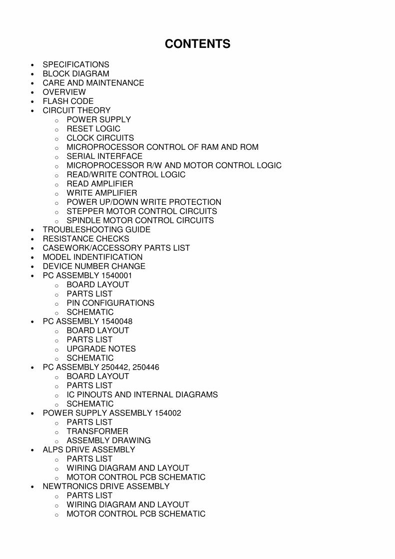
CONTENTS
• SPECIFICATIONS • BLOCK DIAGRAM • CARE AND MAINTENANCE • OVERVIEW • FLASH CODE • CIRCUIT THEORY
o POWER SUPPLY o RESET LOGIC o CLOCK CIRCUITS o MICROPROCESSOR CONTROL OF RAM AND ROM o SERIAL INTERFACE o MICROPROCESSOR R/W AND MOTOR CONTROL LOGIC o READ/WRITE CONTROL LOGIC o READ AMPLIFIER o WRITE AMPLIFIER o POWER UP/DOWN WRITE PROTECTION o STEPPER MOTOR CONTROL CIRCUITS o SPINDLE MOTOR CONTROL CIRCUITS
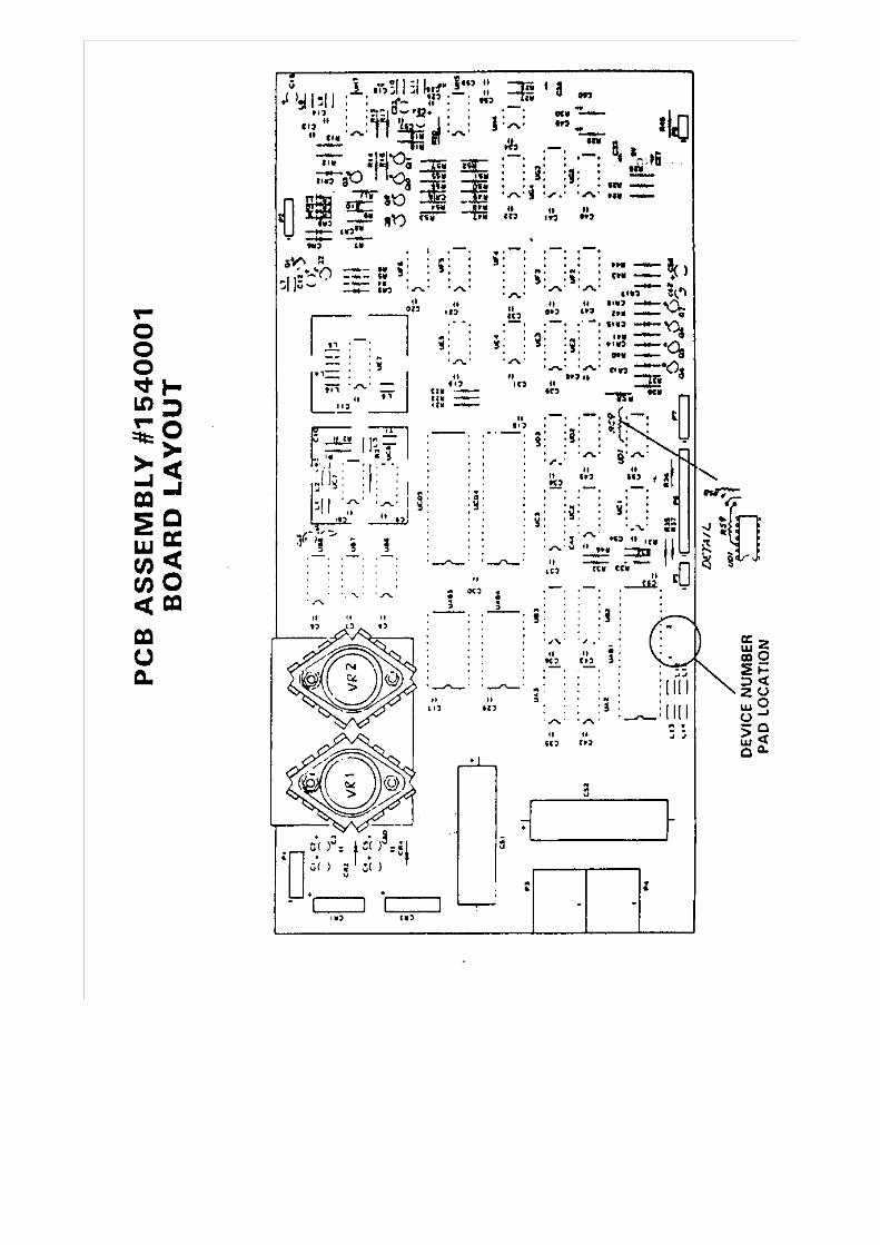
• TROUBLESHOOTING GUIDE • RESISTANCE CHECKS • CASEWORK/ACCESSORY PARTS LIST • MODEL INDENTIFICATION • DEVICE NUMBER CHANGE • PC ASSEMBLY 1540001
o BOARD LAYOUT o PARTS LIST o PIN CONFIGURATIONS o SCHEMATIC
• PC ASSEMBLY 1540048 o BOARD LAYOUT o PARTS LIST o UPGRADE NOTES o SCHEMATIC
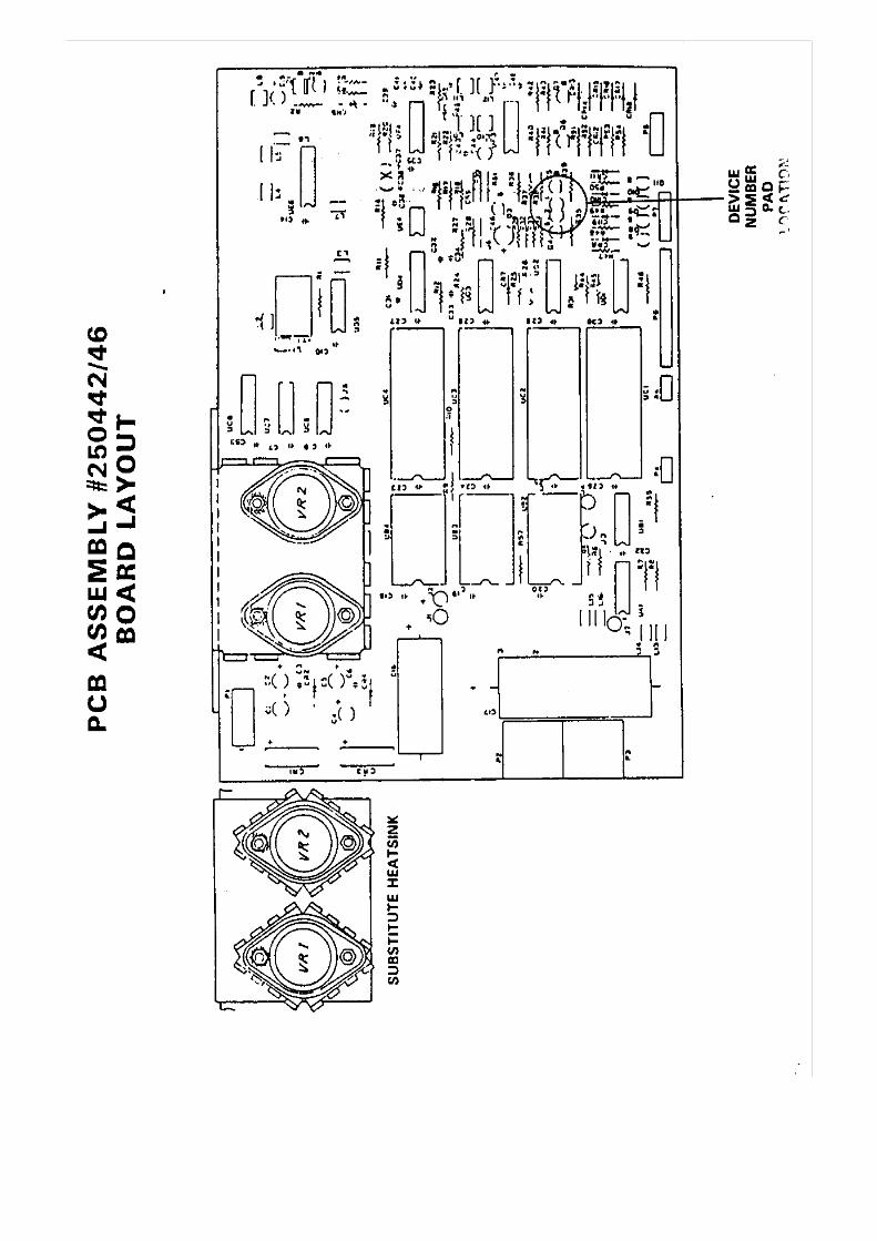
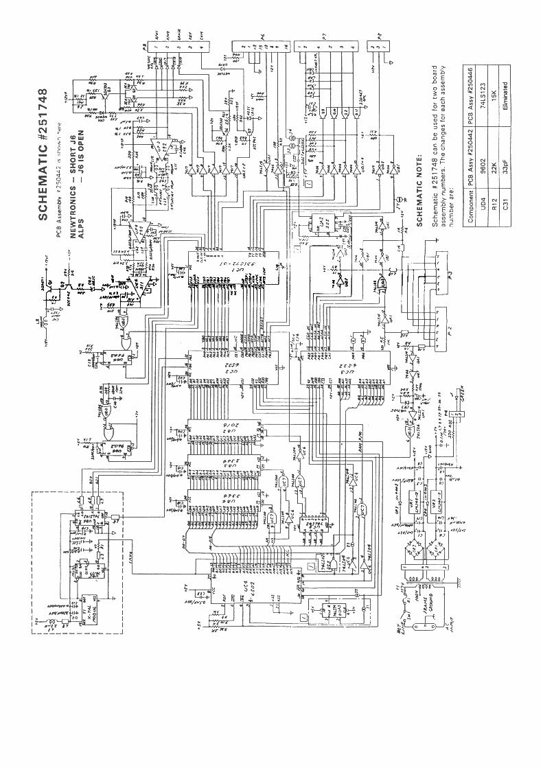
• PC ASSEMBLY 250442, 250446 o BOARD LAYOUT o PARTS LIST o IC PINOUTS AND INTERNAL DIAGRAMS o SCHEMATIC
• POWER SUPPLY ASSEMBLY 154002 o PARTS LIST o TRANSFORMER o ASSEMBLY DRAWING
• ALPS DRIVE ASSEMBLY o PARTS LIST o WIRING DIAGRAM AND LAYOUT o MOTOR CONTROL PCB SCHEMATIC
• NEWTRONICS DRIVE ASSEMBLY o PARTS LIST o WIRING DIAGRAM AND LAYOUT o MOTOR CONTROL PCB SCHEMATIC
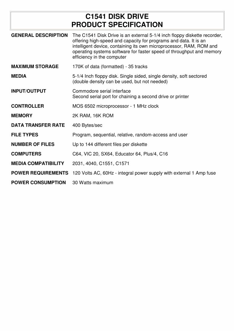
C1541 DISK DRIVE PRODUCT SPECIFICATION
GENERAL DESCRIPTION The C1541 Disk Drive is an external 5-1/4 inch floppy diskette recorder, offering high-speed and capacity for programs and data. It is an intelligent device, containing its own microprocessor, RAM, ROM and operating systems software for faster speed of throughput and memory efficiency in the computer
MAXIMUM STORAGE 170K of data (formatted) - 35 tracks
MEDIA 5-1/4 Inch floppy disk. Single sided, single density, soft sectored (double density can be used, but not needed)
INPUT/OUTPUT Commodore serial interface Second serial port for chaining a second drive or printer
CONTROLLER MOS 6502 microprocessor - 1 MHz clock
MEMORY 2K RAM, 16K ROM
DATA TRANSFER RATE 400 Bytes/sec
FILE TYPES Program, sequential, relative, random-access and user
NUMBER OF FILES Up to 144 different files per diskette
COMPUTERS C64, VIC 20, SX64, Educator 64, Plus/4, C16
MEDIA COMPATIBILITY 2031, 4040, C1551, C1571
POWER REQUIREMENTS 120 Volts AC, 60Hz - integral power supply with external 1 Amp fuse
POWER CONSUMPTION 30 Watts maximum
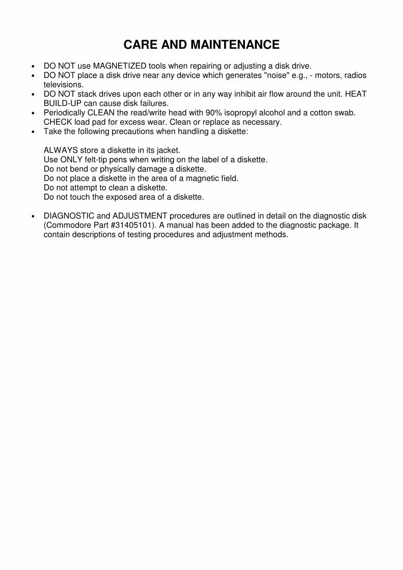
CARE AND MAINTENANCE
• DO NOT use MAGNETIZED tools when repairing or adjusting a disk drive. • DO NOT place a disk drive near any device which generates "noise" e.g., - motors, radios
televisions. • DO NOT stack drives upon each other or in any way inhibit air flow around the unit. HEAT
BUILD-UP can cause disk failures. • Periodically CLEAN the read/write head with 90% isopropyl alcohol and a cotton swab.
CHECK load pad for excess wear. Clean or replace as necessary. • Take the following precautions when handling a diskette:
ALWAYS store a diskette in its jacket. Use ONLY felt-tip pens when writing on the label of a diskette. Do not bend or physically damage a diskette. Do not place a diskette in the area of a magnetic field. Do not attempt to clean a diskette. Do not touch the exposed area of a diskette.
• DIAGNOSTIC and ADJUSTMENT procedures are outlined in detail on the diagnostic disk (Commodore Part #31405101). A manual has been added to the diagnostic package. It contain descriptions of testing procedures and adjustment methods.
OVERVIEW
The drive itself an independent memory device. THe drive is composed of a media clamp rotating mechanism, a head positioning mechanism and an eject mechanism. All positioning operations, excluding insertion and removal of diskettes, are controlled by the internal guide mechanism. Closing the front door causes the media clamp mechanism to operate. Two operations are performed in the following order: a)
The diskette is centered. b)
The diskette is clamped and retained between the spindle and the hub. The spindle and hub rotates at 300 r.p.m. through a closed/loop control circuit employing a D.C motor/tachometer. It is important that the relationship between the head and the media is maintained correctly during operation. For this purpose, a pressure pad is used to hold and press down the media (about 12g) from the opposite side of the head. This head assembly is coupled by a metal band to a four base stepping motor which performs the track positioning. One step of the stepping motor corresponds to a 1/2 track movement. The control circuit on the logic board selects the direction and number of steps to the desired track.
The Read/Write head uses a glass-bonded, ferrite/ceramic head. Track-to-track erasing is accomplished by the straddle erase method. The surface of the Read/Write head is mirror-ground to minimize wear of the head and media. Also, the head is designed in such a way that the maximum signal can be obtained from the media surface.
The spindle drive motor operates on 12 VDC and turns the spindle, through a belt drive, at 300 revolutions per minute. The speed of the drive motor is controlled by a feedback signal from a tachometer, which is housed in the drive motor assembly. The feedback signal controls a servo amp that supplies the 12 VDC drive current.
FLASH CODE
The 1541, upon power-up, goes through its own internal diagnostic. If an electronic problem is detected, it's indicated by flash code. The led's will blink a number of times, pause, and then flash again until the problem is corrected.
Number of flashes Possible failure
2 Zero page
3,4 DOS ROM's
5,6,7,8 RAM
Circuitry associated with these components can also cause the failure code. Therefore, it should be suspected as the next possible defect.
1541 CIRCUIT THEORY
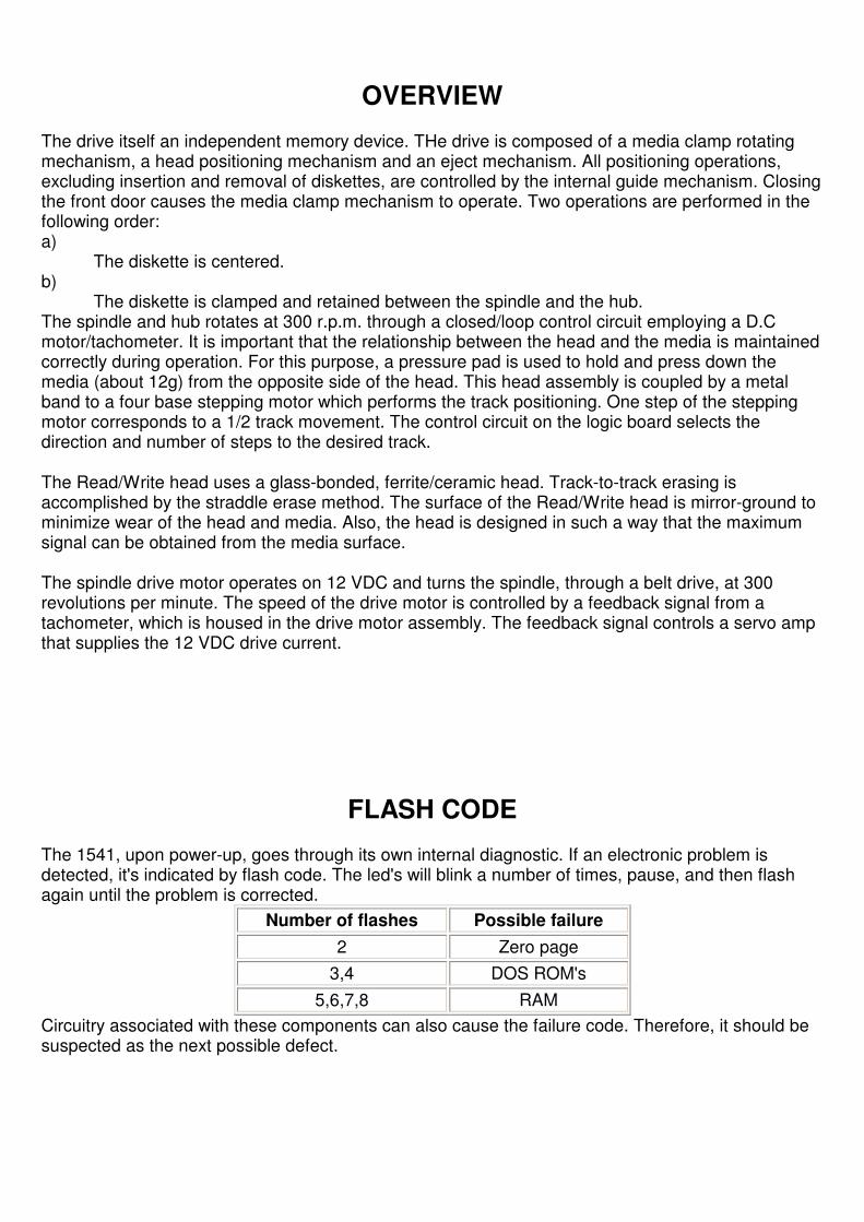
The Power Supply
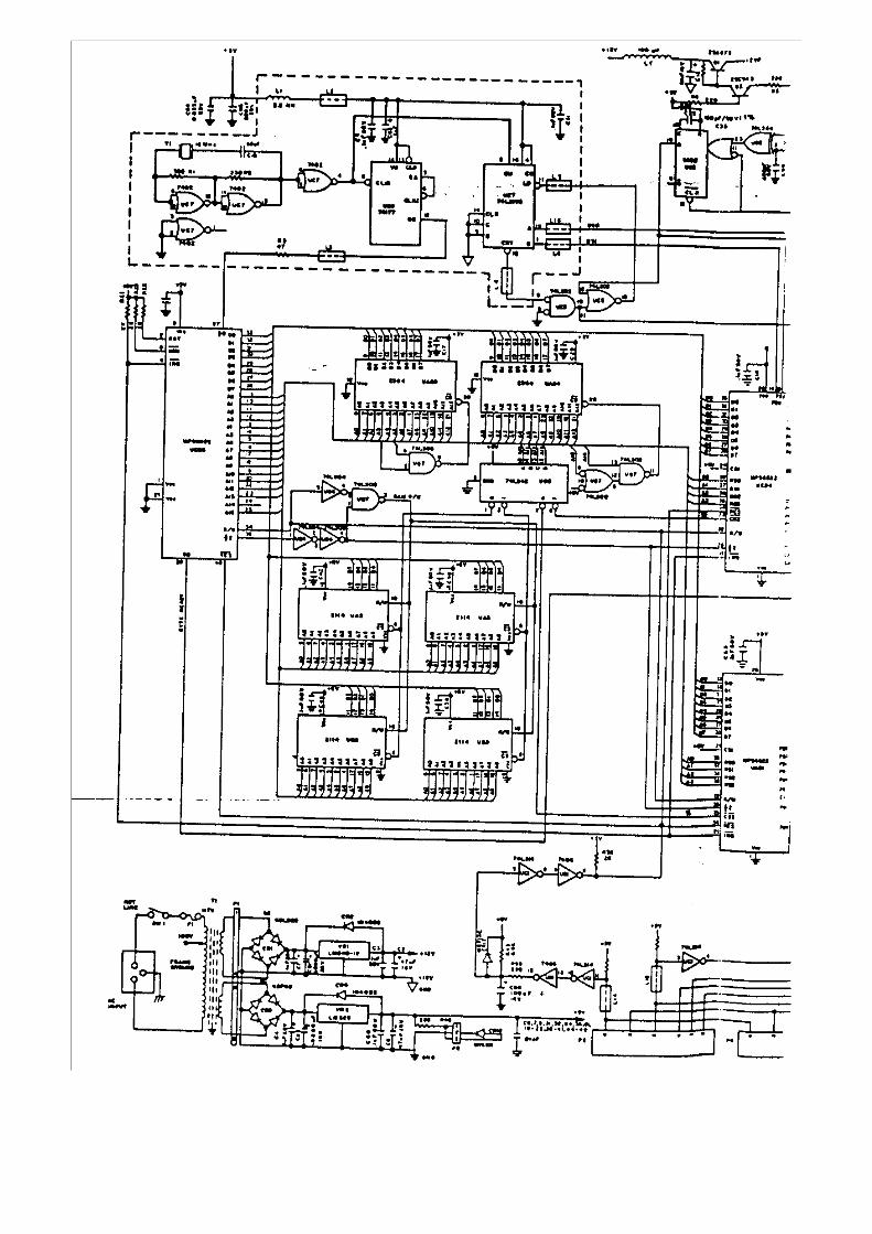
The input AC voltage is controlled by switch 1 (SW1). Disk circuit protection is provided by fuse 1 (F1). If SW1 is closed, the AC voltage input is applied to the primary winding of transformer one (T1). T1 steps down th AC input voltage into two smaller AC voltages. The top secondary AC output (approx. 16VRMS) is converted to DC by the Full Wave Bridge Rectifier CR1. The DC output of CR1 is regulated at 12VDC by VR1. The bottom secondary AC output of T1 (approx. 9VRMS) is converted to DC by the Full Wave Rectifier CR3. The DC output of CR3 is regulated at +5VDC by VR2. High frequency filtering is provided by C1 and C3 for the 12VDC supply, and C4, C6 to C9, C22, C27 to C30 for the 5VDC supply. Low frequency filtering is provided by C17 and C2 for the 12VDC supply, and C5 and C16 for the 5VDC supply.
All circuit diagrams have been taken from the short board schematic 1540049 unless otherwise noted. The short board use a 6116 RAM which replaces the four 2114 I.C.s on the long board. See Read/Write logic differences.
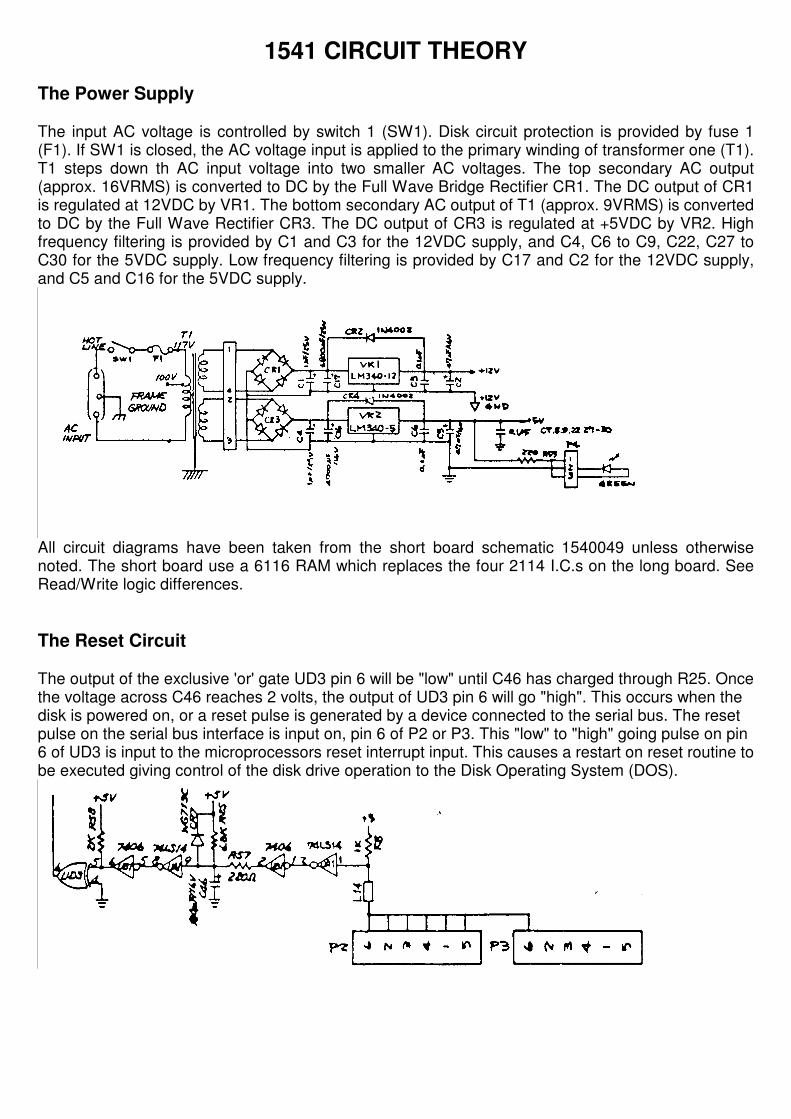
The Reset Circuit
The output of the exclusive 'or' gate UD3 pin 6 will be "low" until C46 has charged through R25. Once the voltage across C46 reaches 2 volts, the output of UD3 pin 6 will go "high". This occurs when the disk is powered on, or a reset pulse is generated by a device connected to the serial bus. The reset pulse on the serial bus interface is input on, pin 6 of P2 or P3. This "low" to "high" going pulse on pin 6 of UD3 is input to the microprocessors reset interrupt input. This causes a restart on reset routine to be executed giving control of the disk drive operation to the Disk Operating System (DOS).
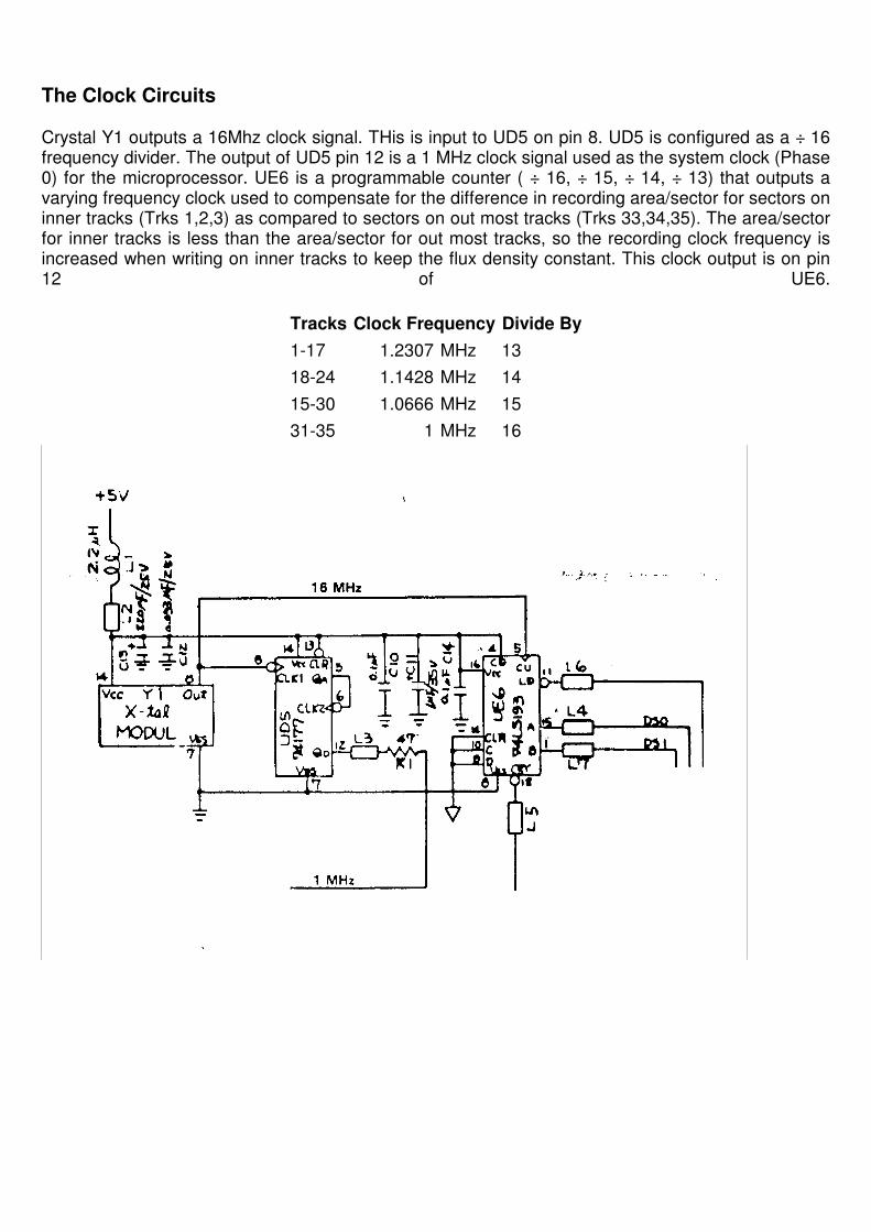
The Clock Circuits
Crystal Y1 outputs a 16Mhz clock signal. THis is input to UD5 on pin 8. UD5 is configured as a ÷ 16 frequency divider. The output of UD5 pin 12 is a 1 MHz clock signal used as the system clock (Phase 0) for the microprocessor. UE6 is a programmable counter ( ÷ 16, ÷ 15, ÷ 14, ÷ 13) that outputs a varying frequency clock used to compensate for the difference in recording area/sector for sectors on inner tracks (Trks 1,2,3) as compared to sectors on out most tracks (Trks 33,34,35). The area/sector for inner tracks is less than the area/sector for out most tracks, so the recording clock frequency is increased when writing on inner tracks to keep the flux density constant. This clock output is on pin 12 of UE6.
Tracks Clock Frequency Divide By
1-17 1.2307 MHz 13
18-24 1.1428 MHz 14
15-30 1.0666 MHz 15
31-35 1 MHz 16
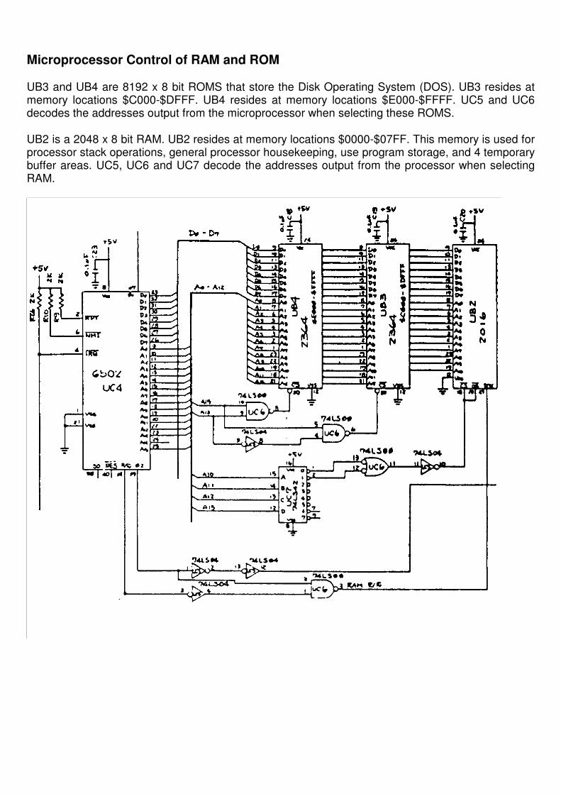
Microprocessor Control of RAM and ROM
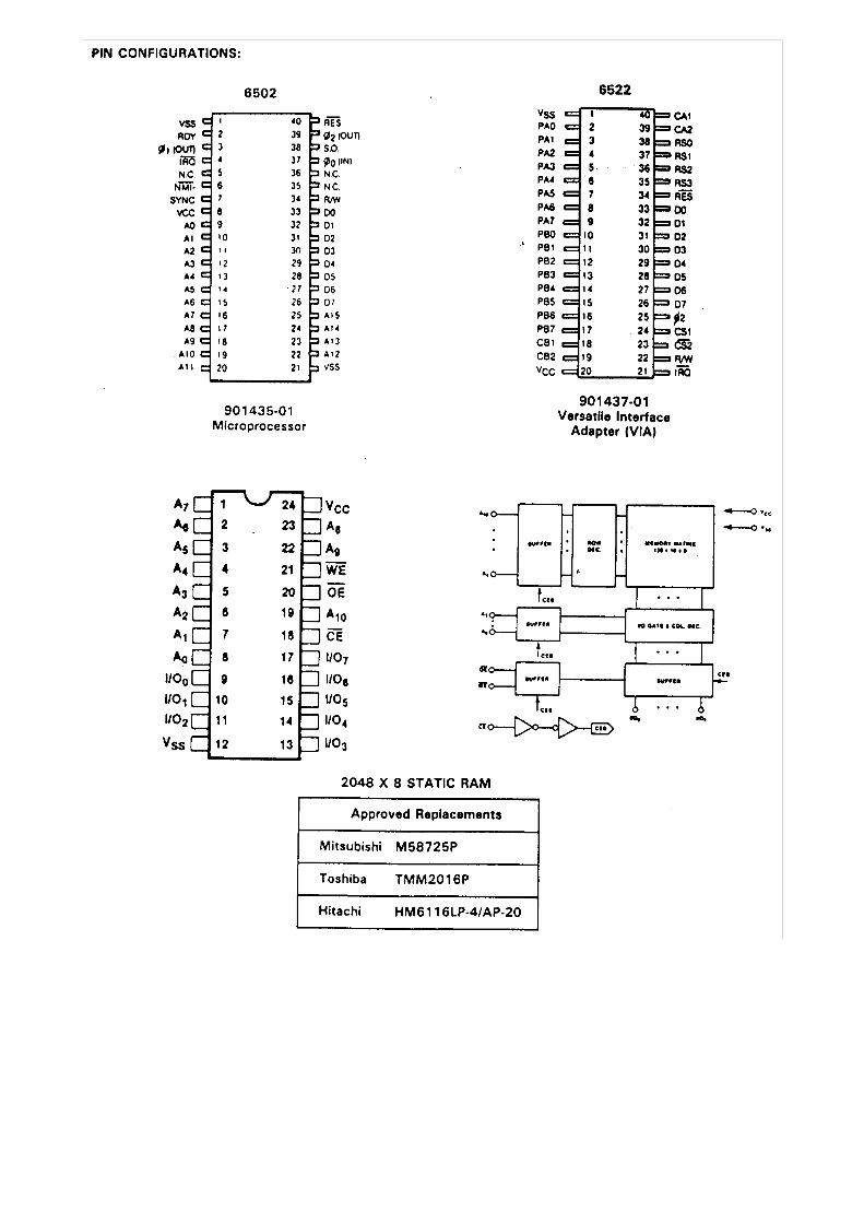
UB3 and UB4 are 8192 x 8 bit ROMS that store the Disk Operating System (DOS). UB3 resides at memory locations $C000-$DFFF. UB4 resides at memory locations $E000-$FFFF. UC5 and UC6 decodes the addresses output from the microprocessor when selecting these ROMS.
UB2 is a 2048 x 8 bit RAM. UB2 resides at memory locations $0000-$07FF. This memory is used for processor stack operations, general processor housekeeping, use program storage, and 4 temporary buffer areas. UC5, UC6 and UC7 decode the addresses output from the processor when selecting RAM.
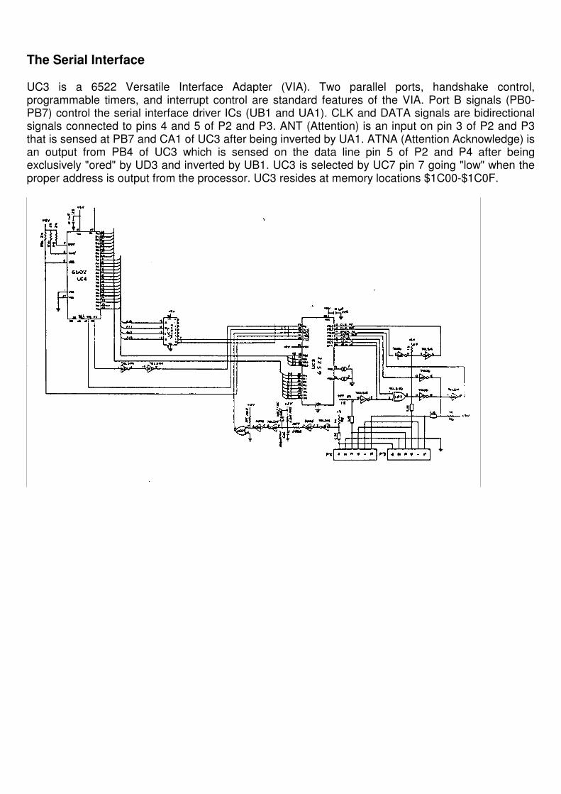
The Serial Interface
UC3 is a 6522 Versatile Interface Adapter (VIA). Two parallel ports, handshake control, programmable timers, and interrupt control are standard features of the VIA. Port B signals (PB0-PB7) control the serial interface driver ICs (UB1 and UA1). CLK and DATA signals are bidirectional signals connected to pins 4 and 5 of P2 and P3. ANT (Attention) is an input on pin 3 of P2 and P3 that is sensed at PB7 and CA1 of UC3 after being inverted by UA1. ATNA (Attention Acknowledge) is an output from PB4 of UC3 which is sensed on the data line pin 5 of P2 and P4 after being exclusively "ored" by UD3 and inverted by UB1. UC3 is selected by UC7 pin 7 going "low" when the proper address is output from the processor. UC3 resides at memory locations $1C00-$1C0F.
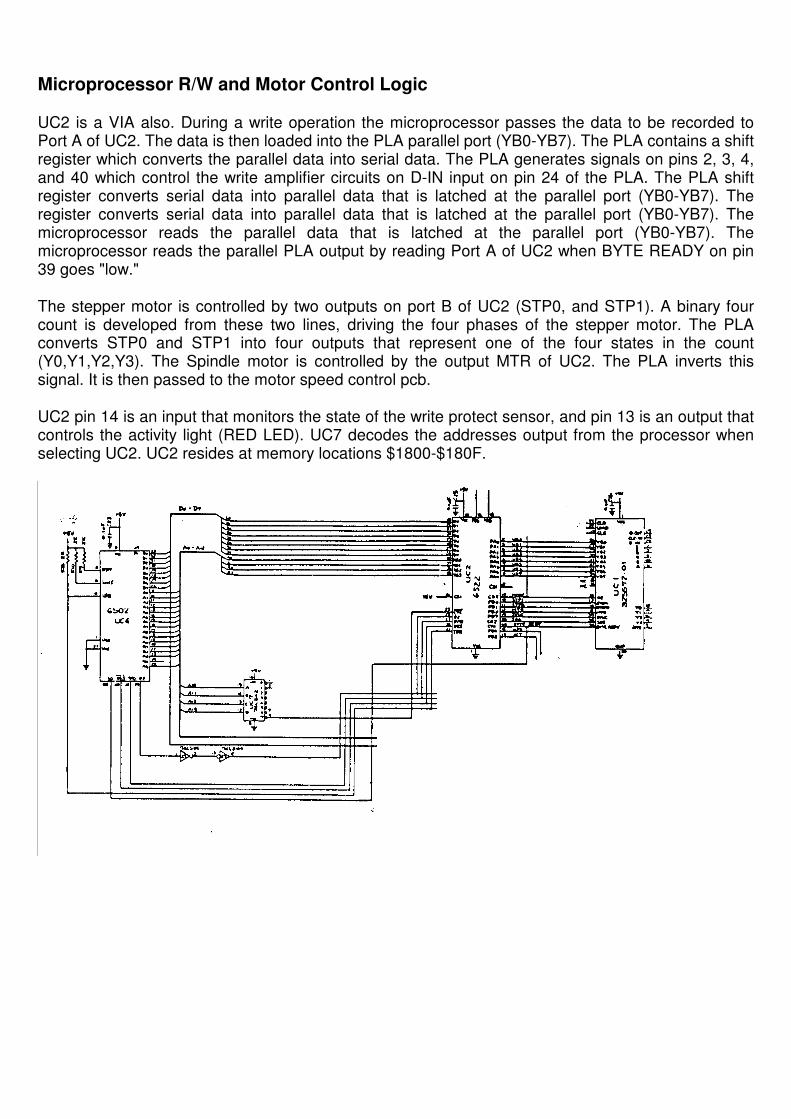
Microprocessor R/W and Motor Control Logic
UC2 is a VIA also. During a write operation the microprocessor passes the data to be recorded to Port A of UC2. The data is then loaded into the PLA parallel port (YB0-YB7). The PLA contains a shift register which converts the parallel data into serial data. The PLA generates signals on pins 2, 3, 4, and 40 which control the write amplifier circuits on D-IN input on pin 24 of the PLA. The PLA shift register converts serial data into parallel data that is latched at the parallel port (YB0-YB7). The register converts serial data into parallel data that is latched at the parallel port (YB0-YB7). The microprocessor reads the parallel data that is latched at the parallel port (YB0-YB7). The microprocessor reads the parallel PLA output by reading Port A of UC2 when BYTE READY on pin 39 goes "low."
The stepper motor is controlled by two outputs on port B of UC2 (STP0, and STP1). A binary four count is developed from these two lines, driving the four phases of the stepper motor. The PLA converts STP0 and STP1 into four outputs that represent one of the four states in the count (Y0,Y1,Y2,Y3). The Spindle motor is controlled by the output MTR of UC2. The PLA inverts this signal. It is then passed to the motor speed control pcb.
UC2 pin 14 is an input that monitors the state of the write protect sensor, and pin 13 is an output that controls the activity light (RED LED). UC7 decodes the addresses output from the processor when selecting UC2. UC2 resides at memory locations $1800-$180F.
Read/Write Control Logic
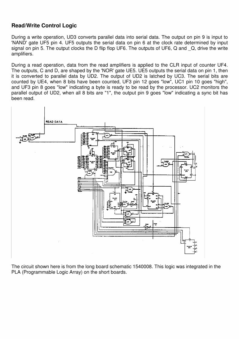
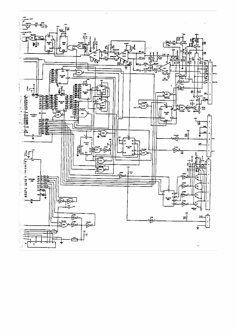
During a write operation, UD3 converts parallel data into serial data. The output on pin 9 is input to 'NAND' gate UF5 pin 4. UF5 outputs the serial data on pin 6 at the clock rate determined by input signal on pin 5. The output clocks the D flip flop UF6. The outputs of UF6, Q and _Q, drive the write amplifiers.
During a read operation, data from the read amplifiers is applied to the CLR input of counter UF4. The outputs, C and D, are shaped by the 'NOR' gate UE5. UE5 outputs the serial data on pin 1, then it is converted to parallel data by UD2. The output of UD2 is latched by UC3. The serial bits are counted by UE4, when 8 bits have been counted, UF3 pin 12 goes "low", UC1 pin 10 goes "high", and UF3 pin 8 goes "low" indicating a byte is ready to be read by the processor. UC2 monitors the parallel output of UD2, when all 8 bits are "1", the output pin 9 goes "low" indicating a sync bit has been read.
The circuit shown here is from the long board schematic 1540008. This logic was integrated in the PLA (Programmable Logic Array) on the short boards.
Read Amplifier Circuits
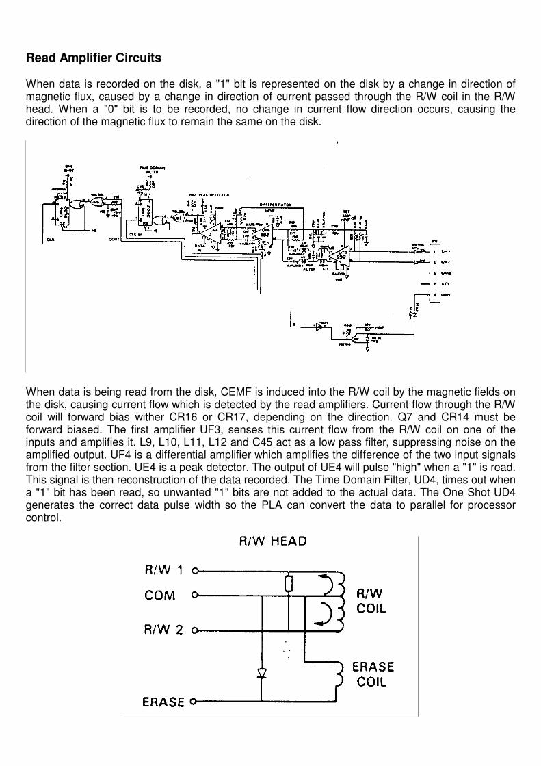
When data is recorded on the disk, a "1" bit is represented on the disk by a change in direction of magnetic flux, caused by a change in direction of current passed through the R/W coil in the R/W head. When a "0" bit is to be recorded, no change in current flow direction occurs, causing the direction of the magnetic flux to remain the same on the disk.
When data is being read from the disk, CEMF is induced into the R/W coil by the magnetic fields on the disk, causing current flow which is detected by the read amplifiers. Current flow through the R/W coil will forward bias wither CR16 or CR17, depending on the direction. Q7 and CR14 must be forward biased. The first amplifier UF3, senses this current flow from the R/W coil on one of the inputs and amplifies it. L9, L10, L11, L12 and C45 act as a low pass filter, suppressing noise on the amplified output. UF4 is a differential amplifier which amplifies the difference of the two input signals from the filter section. UE4 is a peak detector. The output of UE4 will pulse "high" when a "1" is read. This signal is then reconstruction of the data recorded. The Time Domain Filter, UD4, times out when a "1" bit has been read, so unwanted "1" bits are not added to the actual data. The One Shot UD4 generates the correct data pulse width so the PLA can convert the data to parallel for processor control.
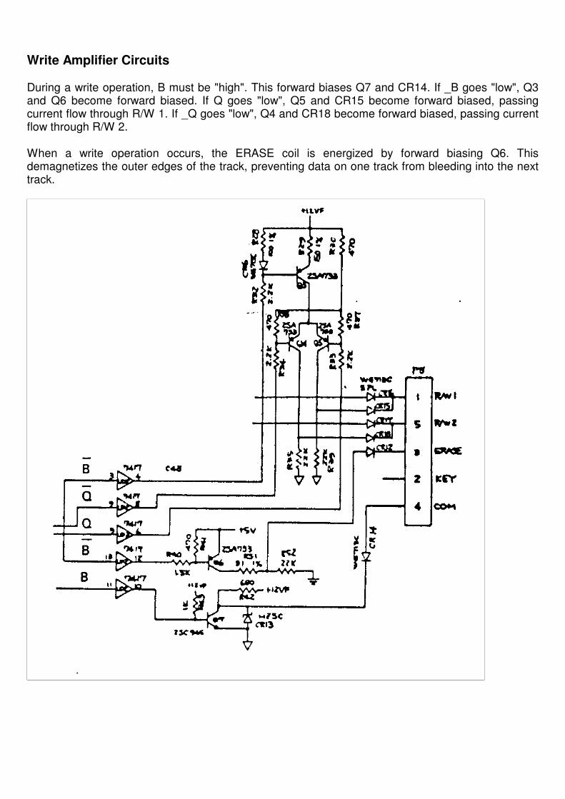
Write Amplifier Circuits
During a write operation, B must be "high". This forward biases Q7 and CR14. If _B goes "low", Q3 and Q6 become forward biased. If Q goes "low", Q5 and CR15 become forward biased, passing current flow through R/W 1. If _Q goes "low", Q4 and CR18 become forward biased, passing current flow through R/W 2.
When a write operation occurs, the ERASE coil is energized by forward biasing Q6. This demagnetizes the outer edges of the track, preventing data on one track from bleeding into the next track.
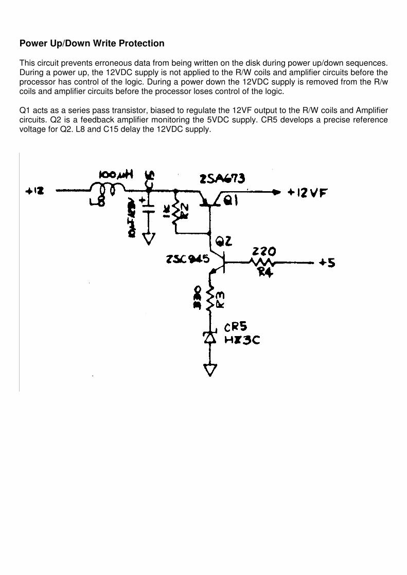
Power Up/Down Write Protection
This circuit prevents erroneous data from being written on the disk during power up/down sequences. During a power up, the 12VDC supply is not applied to the R/W coils and amplifier circuits before the processor has control of the logic. During a power down the 12VDC supply is removed from the R/w coils and amplifier circuits before the processor loses control of the logic.
Q1 acts as a series pass transistor, biased to regulate the 12VF output to the R/W coils and Amplifier circuits. Q2 is a feedback amplifier monitoring the 5VDC supply. CR5 develops a precise reference voltage for Q2. L8 and C15 delay the 12VDC supply.
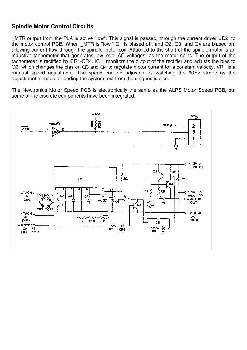
Spindle Motor Control Circuits
_MTR output from the PLA is active "low". This signal is passed, through the current driver UD2, to the motor control PCB. When _MTR is "low," Q1 is biased off, and Q2, Q3, and Q4 are biased on, allowing current flow through the spindle motor coil. Attached to the shaft of the spindle motor is an inductive tachometer that generates low level AC voltages, as the motor spins. The output of the tachometer is rectified by CR1-CR4. IC 1 monitors the output of the rectifier and adjusts the bias to Q2, which changes the bias on Q3 and Q4 to regulate motor current for a constant velocity. VR1 is a manual speed adjustment. The speed can be adjusted by watching the 60Hz strobe as the adjustment is made or loading the system test from the diagnostic disc.
The Newtronics Motor Speed PCB is electronically the same as the ALPS Motor Speed PCB, but some of the discrete components have been integrated.
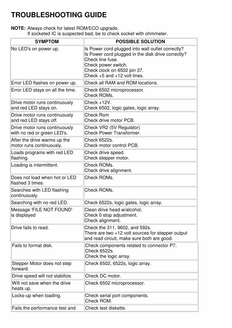
TROUBLESHOOTING GUIDE
NOTE: Always check for latest ROM/ECO upgrade. If socketed IC is suspected bad, be to check socket with ohmmeter.
SYMPTOM POSSIBLE SOLUTION
No LED's on power up. Is Power cord plugged into wall outlet correctly? Is Power cord plugged in the disk drive correctly? Check line fuse. Check power switch. Check clock on 6502 pin 37. Check +5 and +12 volt lines.
Error LED flashes on power up. Check all RAM and ROM locations.
Error LED stays on all the time. Check 6502 microprocessor. Check ROMs.
Drive motor runs continuously and red LED stays on.
Check +12V. Check 6502, logic gates, logic array.
Drive motor runs continuously and red LED stays off.
Check Rom Check drive motor PCB.
Drive motor runs continuously with no red or green LED's.
Check VR2 (5V Regulator) Check Power Transformer.
After the drive warms up the motor runs continuously.
Check 6522s. Check motor control PCB.
Loads programs with red LED flashing.
Check drive speed. Check stepper motor.
Loading is intermittent. Check ROMs. Check drive alignment.
Does not load when hot or LED flashed 3 times.
Check ROMs.
Searches with LED flashing continuously.
Check ROMs.
Searching with no red LED. Check 6522s, logic gates, logic array.
Message 'FILE NOT FOUND' is displayed
Clean drive head w/alcohol. Check 0 stop adjustment. Check alignment.
Drive fails to read. Check the 311, 9602, and 592s. There are two +12 volt sources for stepper output and read circuit, make sure both are good.
Fails to format disk. Check components related to connector P7. Check 6522s. Check the logic array.
Stepper Motor does not step forward.
Check 6502, 6522s, logic array.
Drive speed will not stabilize. Check DC motor.
Will not save when the drive heats up.
Check 6502 microprocessor.
Locks-up when loading. Check serial port components. Check ROM.
Fails the performance test and Check test diskette.
displays a 21 read error. Check Drive Motor.
Fails the performance test and displays a 27 read error.
Check stop adjust.
Passes performance test to track 18 then displays 21 read error.
Check read/write head.
Passes the performance test but will not load certain programs.
Check stepp
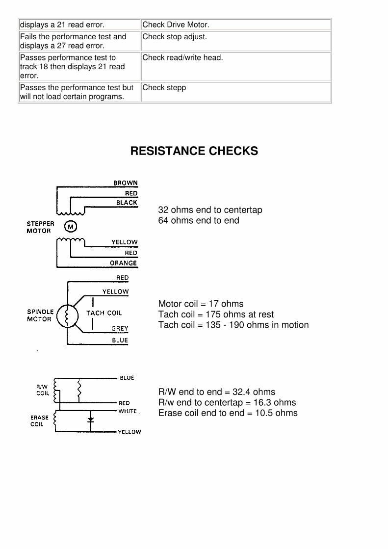
RESISTANCE CHECKS
32 ohms end to centertap 64 ohms end to end
Motor coil = 17 ohms Tach coil = 175 ohms at rest Tach coil = 135 - 190 ohms in motion
R/W end to end = 32.4 ohms R/w end to centertap = 16.3 ohms Erase coil end to end = 10.5 ohms
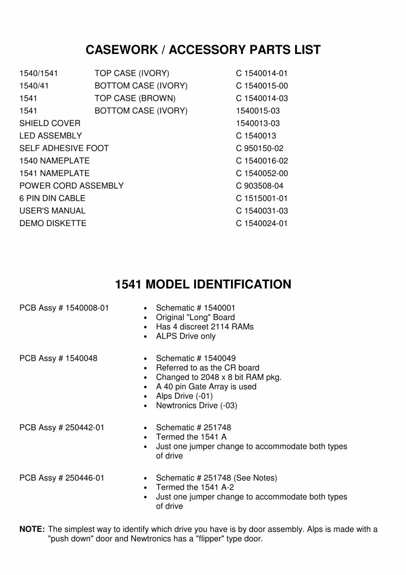
CASEWORK / ACCESSORY PARTS LIST
1540/1541 TOP CASE (IVORY) C 1540014-01
1540/41 BOTTOM CASE (IVORY) C 1540015-00
1541 TOP CASE (BROWN) C 1540014-03
1541 BOTTOM CASE (IVORY) 1540015-03
SHIELD COVER 1540013-03
LED ASSEMBLY C 1540013
SELF ADHESIVE FOOT C 950150-02
1540 NAMEPLATE C 1540016-02
1541 NAMEPLATE C 1540052-00
POWER CORD ASSEMBLY C 903508-04
6 PIN DIN CABLE C 1515001-01
USER'S MANUAL C 1540031-03
DEMO DISKETTE C 1540024-01
1541 MODEL IDENTIFICATION
PCB Assy # 1540008-01 • Schematic # 1540001 • Original "Long" Board • Has 4 discreet 2114 RAMs • ALPS Drive only
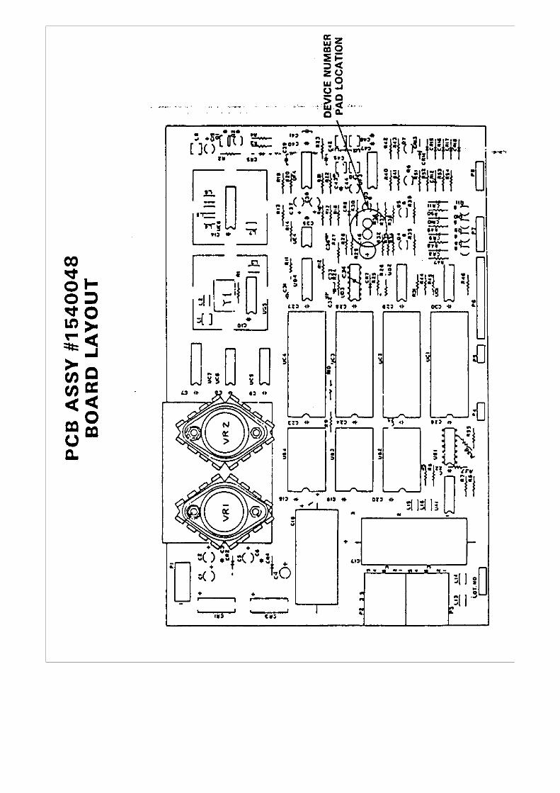
PCB Assy # 1540048 • Schematic # 1540049 • Referred to as the CR board • Changed to 2048 x 8 bit RAM pkg. • A 40 pin Gate Array is used • Alps Drive (-01) • Newtronics Drive (-03)
PCB Assy # 250442-01 • Schematic # 251748 • Termed the 1541 A • Just one jumper change to accommodate both types
of drive
PCB Assy # 250446-01 • Schematic # 251748 (See Notes) • Termed the 1541 A-2 • Just one jumper change to accommodate both types
of drive
NOTE: The simplest way to identify which drive you have is by door assembly. Alps is made with a "push down" door and Newtronics has a "flipper" type door.
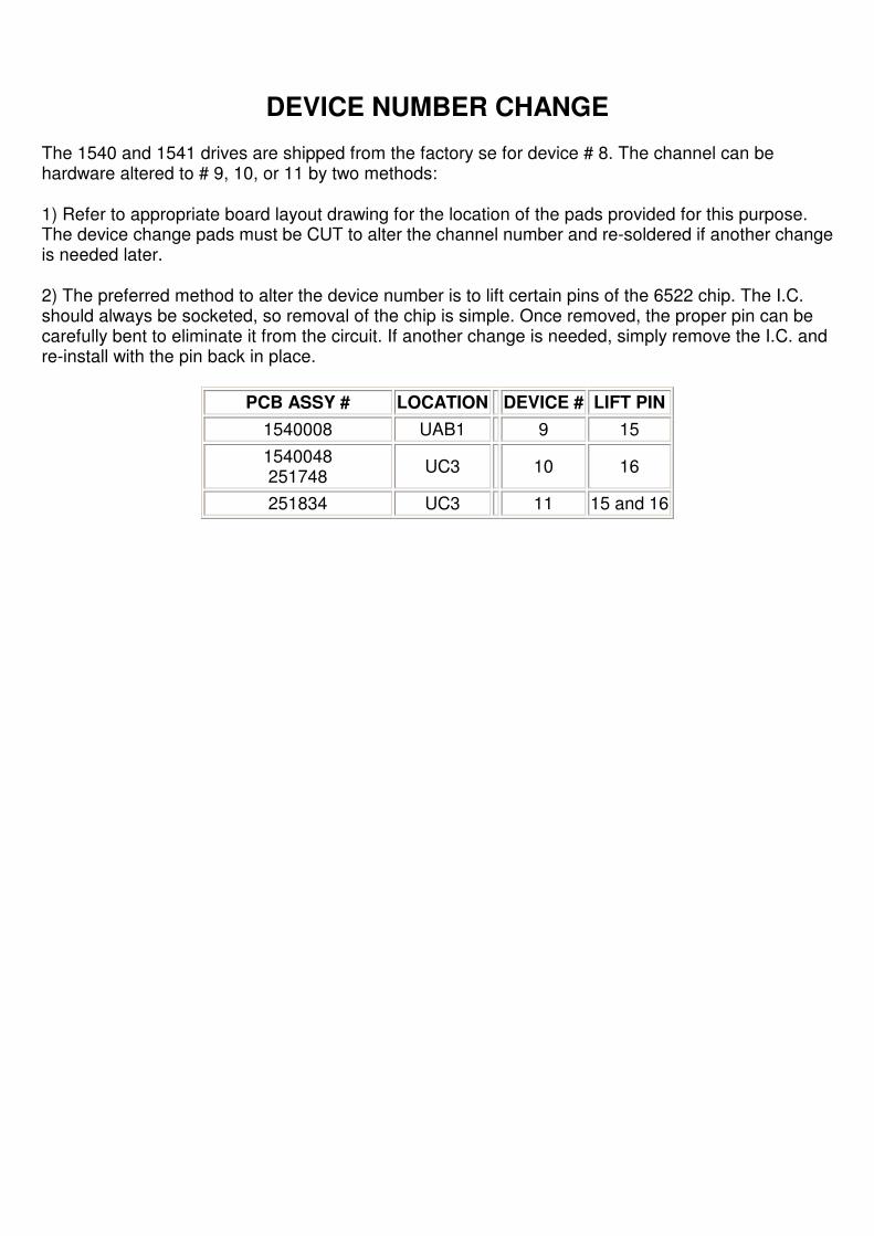
DEVICE NUMBER CHANGE
The 1540 and 1541 drives are shipped from the factory se for device # 8. The channel can be hardware altered to # 9, 10, or 11 by two methods:
1) Refer to appropriate board layout drawing for the location of the pads provided for this purpose. The device change pads must be CUT to alter the channel number and re-soldered if another change is needed later.
2) The preferred method to alter the device number is to lift certain pins of the 6522 chip. The I.C. should always be socketed, so removal of the chip is simple. Once removed, the proper pin can be carefully bent to eliminate it from the circuit. If another change is needed, simply remove the I.C. and re-install with the pin back in place.
PCB ASSY # LOCATION DEVICE # LIFT PIN
1540008 UAB1 9 15
1540048 251748
UC3 10 16
251834 UC3 11 15 and 16
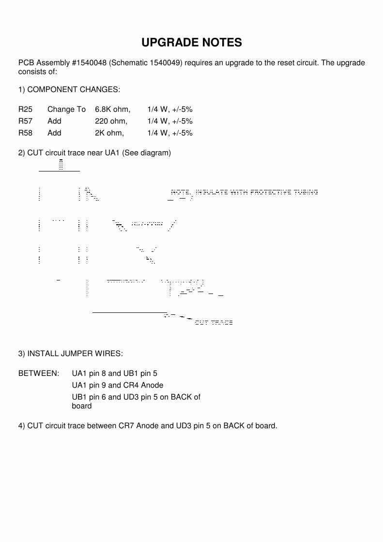
UPGRADE NOTES
PCB Assembly #1540048 (Schematic 1540049) requires an upgrade to the reset circuit. The upgrade consists of:
1) COMPONENT CHANGES:
R25 Change To 6.8K ohm, 1/4 W, +/-5%
R57 Add 220 ohm, 1/4 W, +/-5%
R58 Add 2K ohm, 1/4 W, +/-5%
2) CUT circuit trace near UA1 (See diagram)
3) INSTALL JUMPER WIRES:
BETWEEN: UA1 pin 8 and UB1 pin 5
UA1 pin 9 and CR4 Anode
UB1 pin 6 and UD3 pin 5 on BACK of board
4) CUT circuit trace between CR7 Anode and UD3 pin 5 on BACK of board.
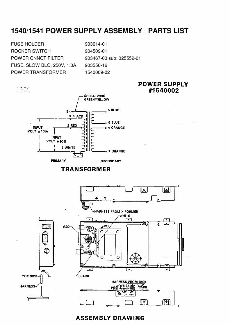
1540/1541 POWER SUPPLY ASSEMBLY PARTS LIST
FUSE HOLDER 903614-01
ROCKER SWITCH 904509-01
POWER CNNCT FILTER 903467-03 sub: 325552-01
FUSE, SLOW BLO, 250V, 1.0A 903556-16
POWER TRANSFORMER 1540009-02
PARTS LIST
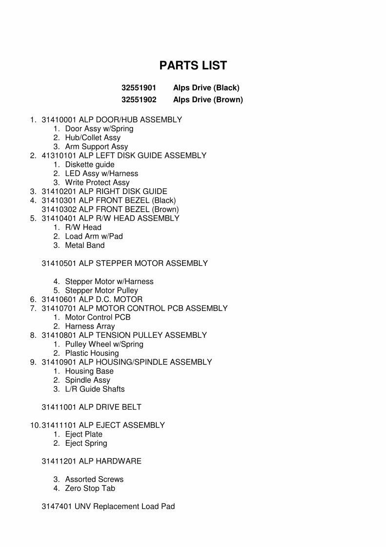
32551901 Alps Drive (Black)
32551902 Alps Drive (Brown)
1. 31410001 ALP DOOR/HUB ASSEMBLY 1. Door Assy w/Spring 2. Hub/Collet Assy 3. Arm Support Assy
2. 41310101 ALP LEFT DISK GUIDE ASSEMBLY 1. Diskette guide 2. LED Assy w/Harness 3. Write Protect Assy
3. 31410201 ALP RIGHT DISK GUIDE 4. 31410301 ALP FRONT BEZEL (Black)
31410302 ALP FRONT BEZEL (Brown) 5. 31410401 ALP R/W HEAD ASSEMBLY
1. R/W Head 2. Load Arm w/Pad 3. Metal Band
31410501 ALP STEPPER MOTOR ASSEMBLY
4. Stepper Motor w/Harness 5. Stepper Motor Pulley
6. 31410601 ALP D.C. MOTOR 7. 31410701 ALP MOTOR CONTROL PCB ASSEMBLY
1. Motor Control PCB 2. Harness Array
8. 31410801 ALP TENSION PULLEY ASSEMBLY 1. Pulley Wheel w/Spring 2. Plastic Housing
9. 31410901 ALP HOUSING/SPINDLE ASSEMBLY 1. Housing Base 2. Spindle Assy 3. L/R Guide Shafts
31411001 ALP DRIVE BELT
10. 31411101 ALP EJECT ASSEMBLY 1. Eject Plate 2. Eject Spring
31411201 ALP HARDWARE
3. Assorted Screws 4. Zero Stop Tab
3147401 UNV Replacement Load Pad
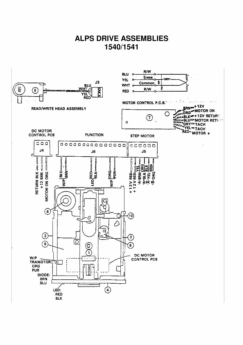
ALPS DRIVE ASSEMBLIES 1540/1541
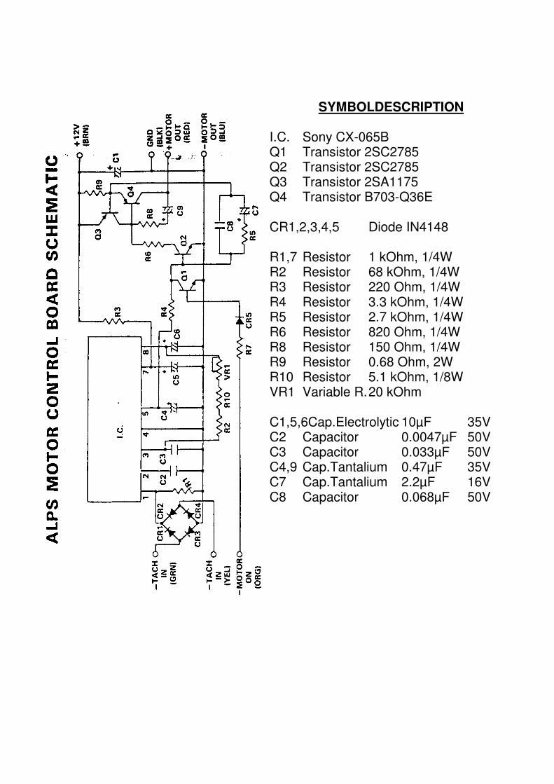
SYMBOLDESCRIPTION I.C. Sony CX-065B Q1 Transistor 2SC2785 Q2 Transistor 2SC2785 Q3 Transistor 2SA1175 Q4 Transistor B703-Q36E CR1,2,3,4,5 Diode IN4148 R1,7 Resistor 1 kOhm, 1/4W R2 Resistor 68 kOhm, 1/4W R3 Resistor 220 Ohm, 1/4W R4 Resistor 3.3 kOhm, 1/4W R5 Resistor 2.7 kOhm, 1/4W R6 Resistor 820 Ohm, 1/4W R8 Resistor 150 Ohm, 1/4W R9 Resistor 0.68 Ohm, 2W R10 Resistor 5.1 kOhm, 1/8W VR1 Variable R. 20 kOhm C1,5,6Cap.Electrolytic 10µF 35V C2 Capacitor 0.0047µF 50V C3 Capacitor 0.033µF 50V C4,9 Cap.Tantalium 0.47µF 35V C7 Cap.Tantalium 2.2µF 16V C8 Capacitor 0.068µF 50V


![Welcome [stllug.sluug.org]tutorial presentation floppy disk diskette Created Date: 1/18/2007 5:58:39 PM](https://img.pdfslide.us/doc/110x75/6071c77c8f6e552afb5c2d8f/welcome-tutorial-presentation-floppy-disk-diskette-created-date-1182007-55839.jpg)