Embed Size (px)
Citation preview

1
REV:00REV:00REV:00REV:00
2002. MAY
MW MW MW MW----ⅡⅡⅡⅡ Series Series Series Series
Service ManualService ManualService ManualService Manual
2
CONTENTS CONTENTS CONTENTS CONTENTS
1.1.1.1. PrefacePrefacePrefacePreface
A. Introductions 3
B. Precautions 3
C. Specifications 4
D. Sealing Method 5
2.2.2.2. Calibration & program code downloadCalibration & program code downloadCalibration & program code downloadCalibration & program code download
A. General calibration 6
B. Calibration block diagram 9
C. How to confirm the setting value 10
D. Program code download 11
3.3.3.3. The schematics and the diagramThe schematics and the diagramThe schematics and the diagramThe schematics and the diagram
A. System Block Diagram 13
B. Circuit Diagram 14
C. Wiring Diagram 18
D. Parts locations 21
E. Exploded View 25
4.4.4.4. The error messagesThe error messagesThe error messagesThe error messages
A. Error message 26
B. Troubleshooting 27
5.5.5.5. Serial Serial Serial Serial InterfaceInterfaceInterfaceInterface
A. RS232C connection 28
6.6.6.6. Parts ListParts ListParts ListParts List
A. Electronic Parts List 30
B. Mechanical Parts List 33
3
1111.... PREFACEPREFACEPREFACEPREFACE
AAAA. . . . IntroductionsIntroductionsIntroductionsIntroductions
Thank you for purchasing our CAS MW-II Series.
These series has been designed with CAS reliability, under rigid quality control
and with outstanding performance. Your specialty departments can enjoy
these high quality reliable CAS products.
We believe that your needs will be satisfied and you will have proper reliability.
This manual will help you with proper operation and care of the MW-II series.
Please keep it handy for future reference.
B. B. B. B. PrecautionsPrecautionsPrecautionsPrecautions
1. Make sure that you plug your scale into the proper power outlet.
2. Place the scale on a flat and stable surface.
3. Plug into a power outlet one hour before operations.
4. Keep the scale away from strong EMI noises may cause incorrect weight readings.
5. This scale must be installed in a dry and liquid free environment.
6. Do not subject the scale to sudden temperature changes.
7. Do not subject the platter to sudden shocks.
8. If the scale is not properly level, please adjust the 4 legs at the bottom of the scale (turn legs
clockwise or counterclockwise) so as to center the bubble of the leveling gauge inside the indicated
circle.
4
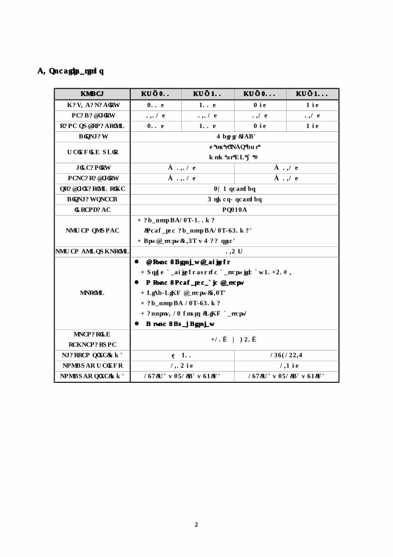
CCCC. . . . SpecificationsSpecificationsSpecificationsSpecifications
MODELMODELMODELMODEL MWMWMWMWⅡⅡⅡⅡ200200200200 MWMWMWMWⅡⅡⅡⅡ300300300300 MWMWMWMWⅡⅡⅡⅡ2000200020002000 MWMWMWMWⅡⅡⅡⅡ3000300030003000
MAX. CAPACITY 200 g 300 g 2 kg 3 kg
READABILITY 0.01 g 0.01 g 0.1 g 0.1 g
TARE SUBTRACTION 200 g 300 g 2 kg 3 kg
DISPLAY 6 digit (LCD)
WEIGHING UNIT g,oz,tI,PCS,dwt,
mom,ct,GN,lb,%
LINEARITY ± 0.01 g ± 0.1 g
REPEATABILITY ± 0.01 g ± 0.1 g
STABILIZATION TIME 2~3 seconds
DISPLAY SPEED 5 times/ seconds
INTERFACE RS232C
POWER SOURCE
- Adaptor DC12V/300mA
(Recharge Adaptor DC12V/850mA)
- Dry Battery (1.5V x 6 AA size)
POWER CONSUMPTION 0.4 W
OPTION
B Type : Display B Type : Display B Type : Display B Type : Display BacklightBacklightBacklightBacklight
- Using backlight cut the battery life by 30-40%.
R Type : R Type : R Type : R Type : Rechargeable BatteryRechargeable BatteryRechargeable BatteryRechargeable Battery
- NiCd/NiMH Battery (7.2V)
- Adaptor DC 12V/850mA
- Approx. 12 hours (NiMH battery)
D type : Dual DisplayD type : Dual DisplayD type : Dual DisplayD type : Dual Display
OPERATING
TEMPERATURE -10 ~ +40
PLATTER SIZE(mm) Φ 300 158*144.6
PRODUCT WEIGHT 1.04 kg 1.3 kg
PRODUCT SIZE(mm) 189(W) x 271(D) x 83(H) 189(W) x 271(D) x 83(H)
5
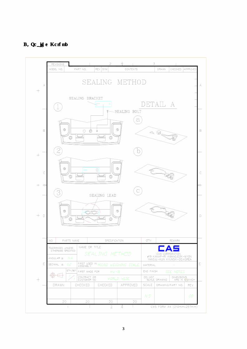
D. Sealing MethodD. Sealing MethodD. Sealing MethodD. Sealing Method
6
2. 2. 2. 2. Calibration Calibration Calibration Calibration & Program code download& Program code download& Program code download& Program code download
A. General calibrationA. General calibrationA. General calibrationA. General calibration
1.1.1.1. Span Span Span Span Calibration Calibration Calibration Calibration ---- “C.SPAN” “C.SPAN” “C.SPAN” “C.SPAN”
1) CALCALCALCAL Switch is located in the battery cover at the bottom of the scale.
While pressing the switch, turn on the power then you will go to calibration mode.
2) The display will shows “CALMod”“CALMod”“CALMod”“CALMod” three times and “C.SPAN”“C.SPAN”“C.SPAN”“C.SPAN”.
3) Press the SETSETSETSET key to go to ““““C. SPANC. SPANC. SPANC. SPAN”””” menu.
4) The display will shows “UNLOAd”“UNLOAd”“UNLOAd”“UNLOAd” then press the SETSETSETSET key. Note that there is nothing on the
platter. If you want to cancel this span calibration, press the ZERO ZERO ZERO ZERO key.
5) Press the SETSETSETSET key, then the display shows “StAbLE”“StAbLE”“StAbLE”“StAbLE”. Note that the scale should be stable.
6) When the display shows “LOAd”“LOAd”“LOAd”“LOAd”, place the weight of maximum capacity on the platter then
press the SETSETSETSET key.
7) The display shows “StAbLE”“StAbLE”“StAbLE”“StAbLE” and “End”“End”“End”“End” then span calibration is finished.
2 2 2 2.... CCCCapacity apacity apacity apacity ---- “C.CAPA” “C.CAPA” “C.CAPA” “C.CAPA”
1) Press the MODEMODEMODEMODE key until the display shows “C.CAPA”“C.CAPA”“C.CAPA”“C.CAPA” menu in the calibration mode.
2) Press the SETSETSETSET key to go to “C.CAPA”“C.CAPA”“C.CAPA”“C.CAPA” menu.
3) Press the MODEMODEMODEMODE key until the display shows maximum capacity of your scale.
4) Press the SETSETSETSET key to save. If you want to cancel, press the ZEROZEROZEROZERO key.
5) Note that the capacity is set to 300 g300 g300 g300 g by default.
3 3 3 3.... Trimming Trimming Trimming Trimming (Multi-Point Calibration) - “C.triM”“C.triM”“C.triM”“C.triM”
1) Press the MODEMODEMODEMODE key until the display shows “C.triM”“C.triM”“C.triM”“C.triM”menu in the calibration mode.
2) Press the SETSETSETSET key, you will see the internal value.
3) If the internal value is not zero, press the TARETARETARETARE key to set it to zero.
4) Place a weight, M1 on the platter and adjust the value to AD1 by pressing the PRINTPRINTPRINTPRINT or
MODEMODEMODEMODE key. Refer to Table 1. PRINTPRINTPRINTPRINT key is used to increase the value and MODEMODEMODEMODE key is used to
decrease the value.
<Table 1>
WeigWeigWeigWeighthththt Internal Value RangeInternal Value RangeInternal Value RangeInternal Value Range
Capa.Capa.Capa.Capa. MW IIMW IIMW IIMW II----300300300300 MW IIMW IIMW IIMW II----3000300030003000
M1M1M1M1 100g 1000g AD1AD1AD1AD1 99944-100055
M2M2M2M2 200g 2000g AD2AD2AD2AD2 199944-200055
M3M3M3M3 300g 3000g AD3AD3AD3AD3 299944-300055
Capa.Capa.Capa.Capa. MW IIMW IIMW IIMW II----200200200200 MW IIMW IIMW IIMW II----2000200020002000
M1M1M1M1 50g 500g AD1AD1AD1AD1 74944-75055
M2M2M2M2 100g 1000g AD2AD2AD2AD2 149944-150055
M3M3M3M3 200g 2000g AD3AD3AD3AD3 299944-300055
7
5) If the value is within AD1, the display shows “ZERO”“ZERO”“ZERO”“ZERO” but if the value is out of this range, it is
impossible to adjust this value.
6) Place a weight, M2 on the platter and adjust the value to AD2 by pressing the PRINTPRINTPRINTPRINT or
MODEMODEMODEMODE key. Refer to Table 1.
7) If the value is within AD2, the display shows “NET”“NET”“NET”“NET”.
8) Place a weight, M3 on the platter and adjust the value to AD3 by pressing the PRINTPRINTPRINTPRINT or
MODEMODEMODEMODE key. Refer to Table 1.
9) If the value is within AD3, the display shows “Battery”“Battery”“Battery”“Battery”.
10) Press the SETSETSETSET key to save it. If you want to cancel, press the ZEROZEROZEROZERO key.
4 4 4 4.... Option (Backlight) Option (Backlight) Option (Backlight) Option (Backlight) ---- “C.OPtbL”
1) Press the MODEMODEMODEMODE key until the display shows “C.O“C.O“C.O“C.OPPPPtbL”tbL”tbL”tbL”in calibration mode.
2) Press the SET SET SET SET key, the display shows “OFF” “OFF” “OFF” “OFF” or or or or “On”“On”“On”“On”.
3) You can change this setting by pressing MODEMODEMODEMODE key. Press the SETSETSETSET key to save. If you want to
cancel, press the ZEZEZEZERORORORO key.
- ON : It is available to use backlight
- OFF : It is not available to use backlight
Note that backlight is set to OFFOFFOFFOFF by default.
5555.... Zero RangeZero RangeZero RangeZero Range - “C.ZPASS”
This is an allowable range from calibrated zero that the scale goes to zero from at start up.
1) Press the MODEMODEMODEMODE key until the display shows “C.ZPASS”“C.ZPASS”“C.ZPASS”“C.ZPASS” in calibration mode.
2) Press the SET SET SET SET key, the display shows “10 PEr”“10 PEr”“10 PEr”“10 PEr”or (“2 PEr”)(“2 PEr”)(“2 PEr”)(“2 PEr”).
3) You can change this setting by pressing MODEMODEMODEMODE key.
- 10 PEr : Zero range is 10% of maximum capacity.
- 2 PEr : Zero range is 2% of maximum capacity.
Note that zero range is set to 10 PEr10 PEr10 PEr10 PEr by default.
4) Press the SETSETSETSET key to save it.
6.6.6.6. UnitUnitUnitUnit - “C.Unit”
1) Press the MODEMODEMODEMODE key until the display shows “C.“C.“C.“C.UnitUnitUnitUnit”””” in calibration mode.
2) Press the SET SET SET SET key, the display shows “C.“C.“C.“C.U.grAmU.grAmU.grAmU.grAm””””.
3) Press the SET SET SET SET key, the display shows ““““OFFOFFOFFOFF”(“”(“”(“”(“ONONONON”)”)”)”).
4) You can change this setting by pressing MODEMODEMODEMODE key. Press the SETSETSETSET key to save.
- ON: You can use this unit. - OFF : You cannot use this unit.
5) When the display shows “C.U.grAm”, press the MODEMODEMODEMODE key to set other units.
Press the SETSETSETSET key to save.
Note that g, ct, pcs and % are set to ONONONON by default.
8
7.7.7.7. Gravity ConstantGravity ConstantGravity ConstantGravity Constant - “C.“C.“C.“C.GrvtyGrvtyGrvtyGrvty””””
1) Press the MODEMODEMODEMODE key until the display shows “C.“C.“C.“C.GrvtyGrvtyGrvtyGrvty””””in calibration mode.
2) Press the SET SET SET SET keykeykeykey, the display shows ““““C.G.NEwGC.G.NEwGC.G.NEwGC.G.NEwG””””. At this time, press the MODEMODEMODEMODE key. You
will see the ““““C.G.OLdGC.G.OLdGC.G.OLdGC.G.OLdG””””.
C.G.OldGC.G.OldGC.G.OldGC.G.OldG menu : you can enter gravity constant of calibration place.
C.G.NewGC.G.NewGC.G.NewGC.G.NewG menu : you can enter gravity constant of using place.
3) Press the SET SET SET SET key, the display shows “9.XXXXX”.
4) To increase the number, press the MODEMODEMODEMODE key and to go to the right side of digit, press the
SET SET SET SET key. To go to the left side of digit, press the TARETARETARETARE key. At last digit, press the SETSETSETSET key to
save. If the value of fifth decimal place is zero, you have to enter 0.
5) If you want to cancel, press the ZEROZEROZEROZERO key.
6) The value of C.G.OldG is converted to the value of C.G.NewG automatically when you perform
the span calibration.
7) Note that the gravity constant is set to 9.799409.799409.799409.79940 by default.
8. Zero Tracking Level 8. Zero Tracking Level 8. Zero Tracking Level 8. Zero Tracking Level “C.ZtrAC”
1) Press the MODEMODEMODEMODE key until the display shows “C.ZtrAC in calibration mode.
2) Press the SET SET SET SET key, the display shows previous setting value. Press the MODEMODEMODEMODE key to change
this value. (Note that zero tracking level is set to 1.0d1.0d1.0d1.0d by default.)
3) Press the SETSETSETSET key to save.
9. Self 9. Self 9. Self 9. Self----Calibration Calibration Calibration Calibration “C.SELFC”
1) Press the MODEMODEMODEMODE key until the display shows “C.SELFC” in calibration mode.
2) Press the SET SET SET SET key, the display shows previous setting value. Press the MODEMODEMODEMODE key to change
this value. (Note that self calibration is set to ONONONON by default.) If you set it to ON, the scale
performs self calibration every 5 minutes.
3) Press the SETSETSETSET key to save.
10. Version 10. Version 10. Version 10. Version “C.vEr”
1) Press the MODEMODEMODEMODE key until the display shows “C.vEr” in calibration mode.
2) Press the SET SET SET SET key, the display shows the version of the scale (For example, “ V2.00 ”)
3) Press the MODEMODEMODEMODE key, the display shows country code. (For example, “ Std ”- Standard)
4) To exit this mode, press the ZEROZEROZEROZERO key.
11.11.11.11. Reset Reset Reset Reset (Default Setting : Calibration Data) - “C.rESEt”“C.rESEt”“C.rESEt”“C.rESEt”
1) Press the MODEMODEMODEMODE key until the display shows, “C.rESEt”“C.rESEt”“C.rESEt”“C.rESEt”in calibration mode.
2) Press the SET SET SET SET key, the display shows “No”“No”“No”“No”.
3) Press the MODEMODEMODEMODE key, you will see “yES”“yES”“yES”“yES” and press the SETSETSETSET key to reset. All settings are
changed to default but zero and span values are remained. If you want to set these values to
0, press the CAL switch and SETSETSETSET key when the display shows “yES”“yES”“yES”“yES” on step 3).

9
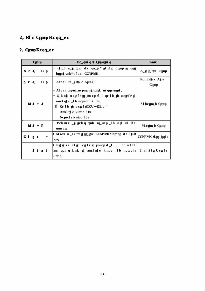
B. CalibratB. CalibratB. CalibratB. Calibration Block Diagramion Block Diagramion Block Diagramion Block Diagram
C .SPA N
C .C A PA
C .triM
U N L O A d L O A d
333300000000gggg
3000g
200g
Internal Value
S
Z
M
S
Z
S
Z
M
S
MMMM WWWW ----IIIIIIII<<<< CCCC aaaalllliiiibbbbrrrraaaattttiiiioooonnnn MMMM ooooddddeeee >>>>
S
Z
2000g
S
C .O ptbL O N /OOOO FFFF FFFF
S
SZ
P
M
: Increase internal Value
: Decrease internal Value
M
S
T : Zero adjustment
M
C .Z PA SS 11110000 PPPP EEEE rrrr / 2 PE r
S
SZ
C .G rvtY C .G .O L dG / C .G .N E w G
S
SZ
C .U nitU nit
(g,ct,oz,lb,tl,dw t,m om ,gn,pcs,% )
S
SZ
C .Z trA C O FF/0.5d/1.0d/2.0d/3.0d/4.0d
S
SZ
vE r “V x.yz, A B C ”
S
SZ
C .rE SE t Y es/NNNN oooo
S
SZ
C .SE L FC O N /O FF
S
SZ
SSSS : SET key ZZZZ : ZERO key TTTT : TARE key MMMM : MODE key PPPP : PRINT key
10
C. How to Confirm the Setting ValueC. How to Confirm the Setting ValueC. How to Confirm the Setting ValueC. How to Confirm the Setting Value
1. Turn on the power and connect the scale to PC with RS232C cable.
2. Open the terminal on PC and adjust COM1, COM 2 and transmission speed to the scale.
3. Press the P P P P on the keyboard of PC then you will hear the beep on the scale. Check the weight
on the terminal.
4. If there is no response on step 3, check the cable, port, transmission speed.
5. Enter 83419 83419 83419 83419 on the PC terminal, you will go to debugging mode.
6. Press Ctrl+RCtrl+RCtrl+RCtrl+R key, you will see the data as below on the PC terminal. If not, enter 83419 slowly.
Keys for debugging mode
CAS MW-2 300 -> Model STD V2.00b -> Code Version Comp. Date : -> Date of Code Compile <= Code Version 2001Mar14-174117 (YYYYMMMDD-HHMMSS) 2001/04/27 16:33:15 -> The Present Time Weight : 779 -> Weight AD(aver) : 25002 -> Internal AD value AD(aver2): 7753 -> (aver - Zp_Cal) * CalFact Zp_Cal : 16518 -> Zero AD valueZero AD valueZero AD valueZero AD value Fp_Cal : 344804 -> Span AD valueSpan AD valueSpan AD valueSpan AD value CalFact : 91383 -> (300000 / (Span - Zero)) * 100000 LSpanDif0: 0 -> Multi-Calibration Data LSpanDif1: 0 -> Multi-Calibration Data FactGap0 : 0 -> Multi-Calibration Data FactGap1 : 0 -> Multi-Calibration Data FactGap2 : 0 -> Multi-Calibration Data Capa. : 0 -> Capacity(0-3) Ini_ZeroV: -37 -> Initial Zero Buffer Z_Buf : 0 -> Rezero Buffer T_Buf : 0 -> Tare Buffer T0_Cnt70m: 65 -> Timer0 T1_Cnt70m: 0 -> Timer1 GravityO : 9.7994 -> OLD Gravity Constant(Reference) GravityN : 9.7994 -> NEW Gravity Constant Hand_Buf0: 25003 -> AD Buffer Hand_Buf1: 25006 : Hand_Buf8: 25003 Hand_Buf9: 25003
KeysKeysKeysKeys DescriptionsDescriptionsDescriptionsDescriptions
Ctrl + R Report
Ctrl + E EEPROM Erase
X EEPROM Read
A ADC(CS5522) Initializing
D Display Buffer Read
11
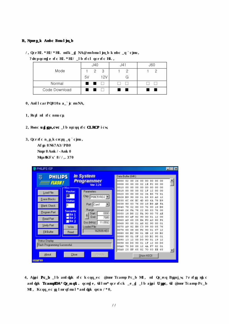
D. Program Code DownloadD. Program Code DownloadD. Program Code DownloadD. Program Code Download
1. Set J40, J41, J60 of main PCB to download mode as below.
After setting the J40, J41 and then set the J60.
J40 J41 J60
Mode 1 2 3
5V 12V
1 2
G
1 2
Normal
Code Download
2. Connect RS232c cable to PC.
3. Turn on the power.
4. Type winiwiniwiniwinissssp.exep.exep.exep.exe and press the ENTERENTERENTERENTER key.
5. Set the parameters as below.
Chip : P89C51RD2
Port : Com1/Com2
Osc(MHz) : 11.0592
6. Click ReadReadReadRead and confirm the message "Boot Vector Read OK." on Status Display. At this time
confirm Vector:FCVector:FCVector:FCVector:FC, Status:00Status:00Status:00Status:00 setting. If not, set them again and click WriteWriteWriteWrite. If "Boot Vector Read
OK." Message is not shown, confirm step 1, 2.

12
7. Click Load FileLoad FileLoad FileLoad File.
8. Click Erase BlocksErase BlocksErase BlocksErase Blocks.
9. Click Select AllSelect AllSelect AllSelect All and then ERASE!ERASE!ERASE!ERASE!.
9. Click Blank CheckBlank CheckBlank CheckBlank Check, Program PartProgram PartProgram PartProgram Part and Verify PartVerify PartVerify PartVerify Part.
10. Turn off the power and set J40, J41, J60 to Normal Mode.
11. Turn on the power and check the operation.
13
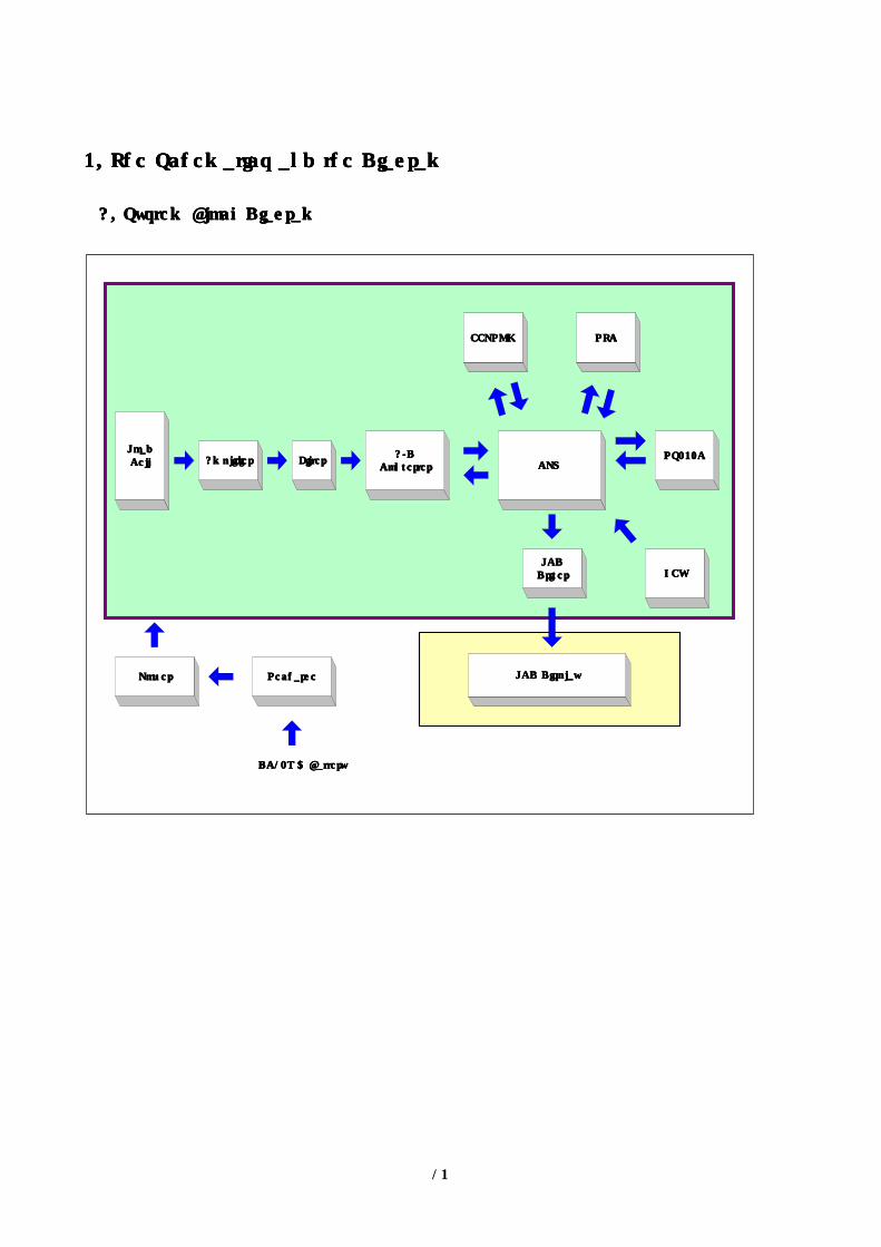
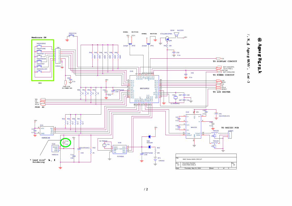
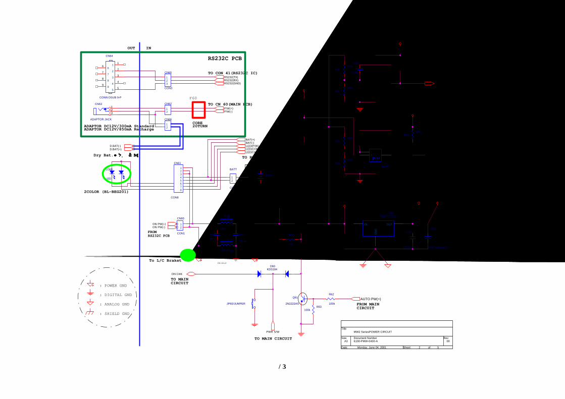
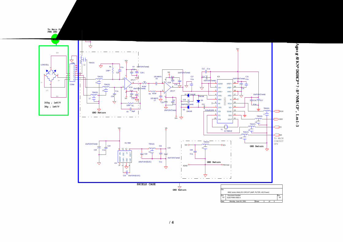
3.3.3.3. The The The The SSSSchematics and the chematics and the chematics and the chematics and the DDDDiagiagiagiagram ram ram ram
A. A. A. A. SSSSystem ystem ystem ystem BlBlBlBlockockockock D D D Diagramiagramiagramiagram
CPUCPUCPUCPUA/DA/DA/DA/D
ConverterConverterConverterConverter
LoadLoadLoadLoadCellCellCellCell AmplifierAmplifierAmplifierAmplifier FilterFilterFilterFilter
EEPROMEEPROMEEPROMEEPROM RTCRTCRTCRTC
RS232CRS232CRS232CRS232C
KEYKEYKEYKEYLCDLCDLCDLCDDriverDriverDriverDriver
LCD DisplayLCD DisplayLCD DisplayLCD DisplayPowerPowerPowerPower RechargeRechargeRechargeRecharge
DC12V & BatteryDC12V & BatteryDC12V & BatteryDC12V & Battery
14
C47
0.1u
TO LCD DRIVER
IC40
89C51RD2
1840 1941 204243
441
2345
6 29303132333435
363738
39
7 8 9
21
10
22
11
23
12
24
13
25
14
26
15
27
16
28
17
WRP0.3 RDP0.2 XTAL2P0.1P0.0
VccN.C
P1.0P1.1P1.2P1.3
P1.4
P2.5
P2.6
P2.7
PSENAL
EN
.CEA
P0.7
P0.6
P0.5
P0.4
P1.5
P1.6
P1.7
XTAL1
RES
ET
vss
RXD
N.C
N.C
P2.0
TXD
P2.1
INT0
/P3.
2
P2.2
INT1
/P3.
3
P2.3
T0/P
3.4
P2.4
T1/P
3.5
RESET
R54
4.7K
VD+
C37
0.1u
BAT CHK(LOW)
R46
100K
C53
0.1u
J40
CON10
12345678
R53
1K
SW40/MODE
TO POWER CIRCUIT
C4120P
C43
0.1u
VD+
C48
0.1u
* Lead wire에에에에 가깝게가깝게가깝게가깝게 Soldering
C52
0.1u
TO POWER D60
CON41
123
SCLK
D40KDS184
SW40/SET
BAT CHK(OFF)
JP41Jumper
R50
1K
C45
0.1u
R52
1K
6100-PMW-0400-A 00
MW2 Series MAIN CIRCUIT
A3
1 5Thursday, May 31, 2001
Title
Size Document Number Rev
Date: Sheet of
R40 10K
R48
100K
Membrane SW
C4020P
CS
SW40
Q40
KTA1298Y(PNP)NORMAL
JP40Jumper
PWR S/W
WRITTING
L41
TDK220
SW41/CAL
MAX232
IC42
1
3
4
5
1112
16
2
6
1413
15
C+
C-
C2+
C2-
T1INR1OUT
VCC V+
V-
T1OUTR1IN
GN
D
C/D
C42
0.1u
R47
100K
L40
TDK220
C5410u/10V(Tantal)
Y41
32.768KHZ
H605215
IC44
1
32
GND
RESETVDD
R57
4.7K
V12+
R45
100K
BUSY
IC41
KM93C46
321
4
5
8
DISKCS
DO
GND
VCC
VD+
C46
0.1u
BZ40 BUZZER
CS
FROM AD
TO DISPLAY CIRCUIT
C4910u/10V(Tantal)
R51
1K
SCLK
VD+
SDI
VD+
R56
4.7K
R44
100K
IC43
PCF8563
321
4 5
8
67
INTOSCOOSCI
vss SDA
VCC
SCLCLKOUT
CS
TO RS232C PCB
C5110u/10V(ELEC)
R55
4.7K
C44
220u/10V(elec)
C36
0.1u
SDO
VD+
R49
100K
AUTO PW(+)
VD+
SI
NORMAL
SW40/ON-OFF
SW40/TARE
BT1
CR2032
ON CHK
C68
0.1u
SW40/ZERO
R42
2K
SW40/PRT
WRITTING
Y40
11.0592MHZ
R43
10K
B.
B.
B.
B. CCC C
ircuit
ircuit
ircuit
ircuit D
iagram
Diagram
Diagram
Diagram
1. M
ain Circuit (C
PU). N
o1/5
15
ACTIVE HIGH
ON CHK
8
BATT
CON2
12
: ANALOG GND
CN64
CONN DSUB 9-P
16
27
38
49
5
16
27
38
49
5
D.BAT(+)
: POWER GND
F60
R69-147k
FROM MAINCIRCUIT
Ni-Cd 7.2V/600mAhNi-MH 7.2V/1300mAh
R62
100k
R612k
Vin
R69100k
ADAPTOR DC12V/850mA Recharge
TO CN 60(MAIN PCB)
TO CON 41(RS232C IC)
2COLOR (BL-BEG201)
C63100uF/16V(ELEC)
Dry Bat.사용시연결사용시연결사용시연결사용시연결
Q61
2N2222AS
CN61
CON8
12345678
Q60
KTA1298Y
6100-PMW-0400-A 00
MW2 SeriesPOWER CIRCUIT
A3
2 5Monday, June 04, 2001
Title
Size Document Number Rev
Date: Sheet of
+-
U61A
213
2.5V
To EL Power
C62
330uF/25V(Elec)
CN62
12
BAT CHK(BAT OFF)
JP60/JUMPER
R69-249.9k
LED(P/W)
ON PW(-)
FROMRS232C PCB
: SHIELD GND
RS232C PCB
D60KDS184
8
C67
C0.1u
접지접지접지접지WIRE
TL062
R6847k
ACTIVE HIGH
: DIGITAL GND
RS232(GND)
TO MAIN CIRCUIT(BAT OFF)
PWR S/W
IN
U607805(TO252)
1 3
2
IN OUT
GN
D
P/W(+)
ON PW(+)
BAT CHK(LOW BAT)
R60
10k
VD+
CN66
12
V12+
BT70
TO MAIN CIRCUIT(LOW BAT)
L61 472u
P/W(-)
LO60
LED
R66100k
+-
U61B
675
R6430k
C61
C0.1u
RS232(TX)
4
VD+
R6730k
LED(CHG)
TO MAINCIRCUIT
20TURN
R63100k
R6520k
VD+
CN60
CON1
12
TO RECHARGE PCB
VD+
ADAPTOR DC12V/300mA Standard
BAT(+)
TO MAIN CIRCUIT
CORE
To L/C Braket
C60C0.1u
C66
C0.1u
L60
472u
CN65
CON3
123
CN63
ADAPTOR JACK
123
RS232(RX)
C64
C0.1u
TL062
VA+
OUT
LED(COM)D.BAT(-)
SHIELD
OPTION
C65
10uF/16V(elec)
BAT(-)
4
AUTO PW(+)
2. P
ower C
ircuit. N
o 2/5
16
VA-
To Main PCBPWR GND
SDI
C17
10uF/10V(Tantal)
LOADCELL
1
2
3
4C18-1
10uF/10V(Tantal)R1
120k**
R4 49.9k*
S+
C9
0.1u
C24
0.1u
GND Return
TO MAINCIRCUITCPU
C22
100uF/16V(ELEC)
P/W Gnd
C14
10uF/10V(Tantal)
+
- IC2A
OP1773
2
6
74
R2120k**
C80.1u
SDO
3Kg ; 1mV/V
VA+
C10
10uF/10V(Tantal)
C3
0.1u
300g ; 1mV/V
C21
0.1u
C28
0.1u
CS
AGND
C19-1
10uF/10V(Tantal)
R3
49.9k*
L7
TDK221
GND Return
VA+
S-
C18
10uF/10V(Tantal)
L9
TDK221
C26
0.1u
SHIELD CASE
GND Return
C11
0.01uF(103)
C110uF/10V(Tantal)
L4
TDK221
D21N4148
C23 10uF/16V(ELEC)
C7105 MMY5
C6105 MMY5
L3
TDK221
C20.1u
VA+
CN1
CON8
12345678
IC3
VA-
EX+
D1 1N4148
C40.1u
GND Return
VA+
SCLK
C12 0.1u
L1TDK221
10uF/10V(Tantal)
C13
CS5522
C19
10uF/10V(Tantal)
L10
TDK221
C16
0.1u
+
6100-PMW-0400-A 00
MW2 series ANALOG CIRCUIT (AMP, FILTER, A/D,Power)
A3
3 5Monday, June 04, 2001
Title
Size Document Number Rev
Date: Sheet of
VA-
접지접지접지접지WIRE
VA+
C20
10uF/10V(Tantal)
+
- IC1A
OP1773
2
6
74
C25
10uF/10V(Tantal)
C150.1u
LC1
C5 30pF
EX-
L6
TDK221 VD+
IC4
ICL7660
8 72 4
5
31
6
VIN
OSC
CAP+
CAP-
VOUT
GND
BOOS
T
LV
L2
TDK221
C270.1u
C29
0.1u
1
2
3
4
5
6
7
8
9
10 11
12
13
14
15
16
17
18
19
20AGND
VA+
AIN1+
AIN1-
NBV
A0
CPD
SDI
CS
XIN XOUT
SDO
DGND
VD+
SCLK
A1
AIN2-
AIN2+
VREF-
VREF+
D3
1N4148
Y132.768KHZ
L5
TDK221
L8
TDK221
VO+
+
3. A
nalog Circuit (A
MP, F
ILTER, A
/D, P
OWER). N
o 3/5
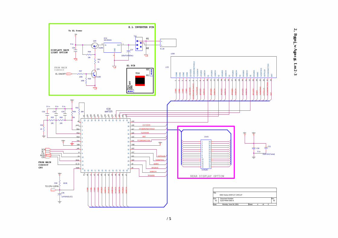
17
5F/G
/E/DGND
Vdo+
R35
10K
DISPLATY BACKLIGHT OPTION
1F/G
/E/D
C37
100uF/16V(Elec)
OZ/T/L/LB
COM
2
Q31
C3198
BAT
O1
PCS/MOM/CT/GNVdo+
IC31S81350HG
13
2
OUTIN
GND
E.L INVERTER PCB
3A/B
/C/H
C30
0.1u
6100-PMW-0400-A 00
MW2 Series DISPLAY CIRCUIT
A3
4 5Monday, June 04, 2001
Title
Size Document Number Rev
Date: Sheet of
VD+
C34
0.1u
Vin
R37
100k
To EL Power
5A/B
/C/H
3F/G
/E/D
3F/G
/E/D
Vdo+
OZ/
T/L/
LB
R38100k
5F/G/E/D
T30
%/D
WT/
KG
FROM MAINCIRCUITCPU
%/DWT/KG
ST/ZERO/NET/HOLD
Q30
A1266
T30
1A/B
/C/H
5A/B/C/H
C31
10uF/10V(Tantal)
3A/B
/C/H
R36
10k
2A/B
/C/H
R611k
2A/B
/C/H
E.L30
o
o
*/LO/OK/HI
C/D
C33
0.1 u
ST/Z
ERO
/NET
/HO
LD
(1)/-/(2)/(3)
TO CPU 12PINR30 49.9K
6F/G/E/D
4A/B
/C/H
COM
2
SI
2F/G
/E/D
4A/B
/C/H
6A/B/C
Vin
6F/G
/E/D
COM
3
C35
1uF/50V(ELEC)
4F/G
/E/D
R31
30K
FROM MAINCIRCUIT
O2
BAT
C32
0.1u
COM
3
BUSY
COM
1
6A/B
/C
PCS/
MO
M/C
T/G
N
O1
R32
1K
EL PCB
1A/B
/C/H
1F/G
/E/D
COM
0
EL ON/OFF
SCK
*/LO
/OK/
HI
(1)/-
/(2)/(
3)
Vdo+
CN70
CON28C
1234567891011121314
2827262524232221201918171615
COM
0
REAR DISPLAY OPTION
O2
LD30
LCD
1 2 3 4 5 6 7 8 9 10 11 12 13 14 15 16 17 18 19 20 21 22 23 24 25 26 27 28
COM
0
COM
1
COM
2
COM
3
(1)/-
/(2)/(
3)
ST/Z
ERO
/NET
/HO
LD
*/LO
/OK/
HI
1F/G
/E/D
1A/B
/C/H
S1 2F/G
/E/D
2A/B
/C/H
S2 3F/G
/E/D
3A/B
/C/H
S3 4F/G
/E/D
4A/B
/C/H
S4 5F/G
/E/D
5A/B
/C/H
S5 6F/G
/E/D
6A/B
/C
%/D
WT/
K/G
OZ/
T/L/
LB
PCS/
MO
M/C
T/G
N
BAT
CS
2F/G
/E/D
COM
1
C36
0.1u
R33
10K
R34
10K
ON/OFF
Vdo+
4F/G
/E/D
IC30upd7225
cl2
_sync
Vlc1
Vlc2
Vlc3
Vss
Vdd
_sck
si
_cs
_busy
C/_D
reset
nc c0 c1 c2 c3 s0 s1 s2 s3 s4 s5 s6 s7
s8
s9
s10
s11
s12
s13
Vdd
s14
s15
s16
s17
s18
s19
s20
s21
s22
s23
s24
s25
s26
s27
s28
s29
s30
s31
cl1
1
2
3
4
5
6
7
8
9
10
11
12
13
14 15 16 17 18 19 20 21 22 23 24 25 26
27
28
29
30
31
32
33
34
35
36
37
38
39
40414243444546474849505152
4. D
isplay C
ircuit. N
o 4/5
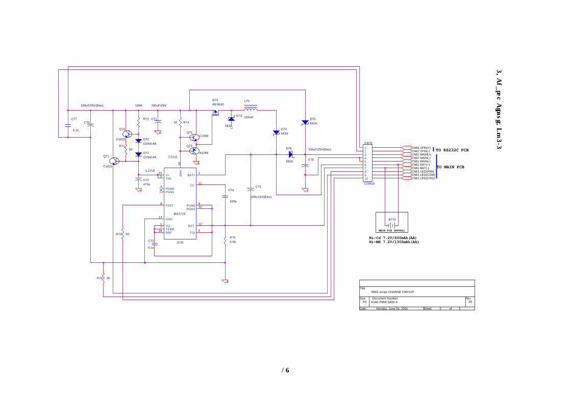
18
D755819
D73
5819
C73
0.1u
R741K
12mACN61 BAT(-)
CN61 MAIN(+)
C76
330uF/25V(Elec)D71D1N4148
C71
330uF/25V
IC70
MAX713
155
34
13
8
1
167
2
11
910
12
6
14V+TH1
PGM0PGM1
GND
FAST
VLI
REFTEMP
BAT+
CC
PGM2PGM3
BAT-
TL0
DR
V
R70 2K
L70
220uH
6140-PMW-0400-0 00
MW2 series CHARGE CIRCUIT
A3
5 5Monday, June 04, 2001
Title
Size Document Number Rev
Date: Sheet of
C75
100u/16V(Elec)
Q71
C1815
D70D1N4148
CN61 LED(COM)
30mA
C77
0.1u
R7150 TO RS232C PCB
CN61 LED(P/W)
CN61 MAIN(-)
D745819
C74
220p
CN62 2PIN(-)
C72470u
CN62 1PIN(+)
MAIN PCB INSTALL
R72
100K
Q73
A1266
Ni-Cd 7.2V/600mAh(AA)Ni-MH 7.2V/1300mAh(AA)
TO MAIN PCBCN61 BAT(+)
R750.66
CN61 MAIN(-)
Q74IRF9530
CN70
CON10
12345678910
R73 50
Q72C1959
C70
330uF/25V(Elec)
D76
5819
BT70
Q70
C1815
CN61 LED(CHG)
5. C
harge Circuit. N
o 5/5
19
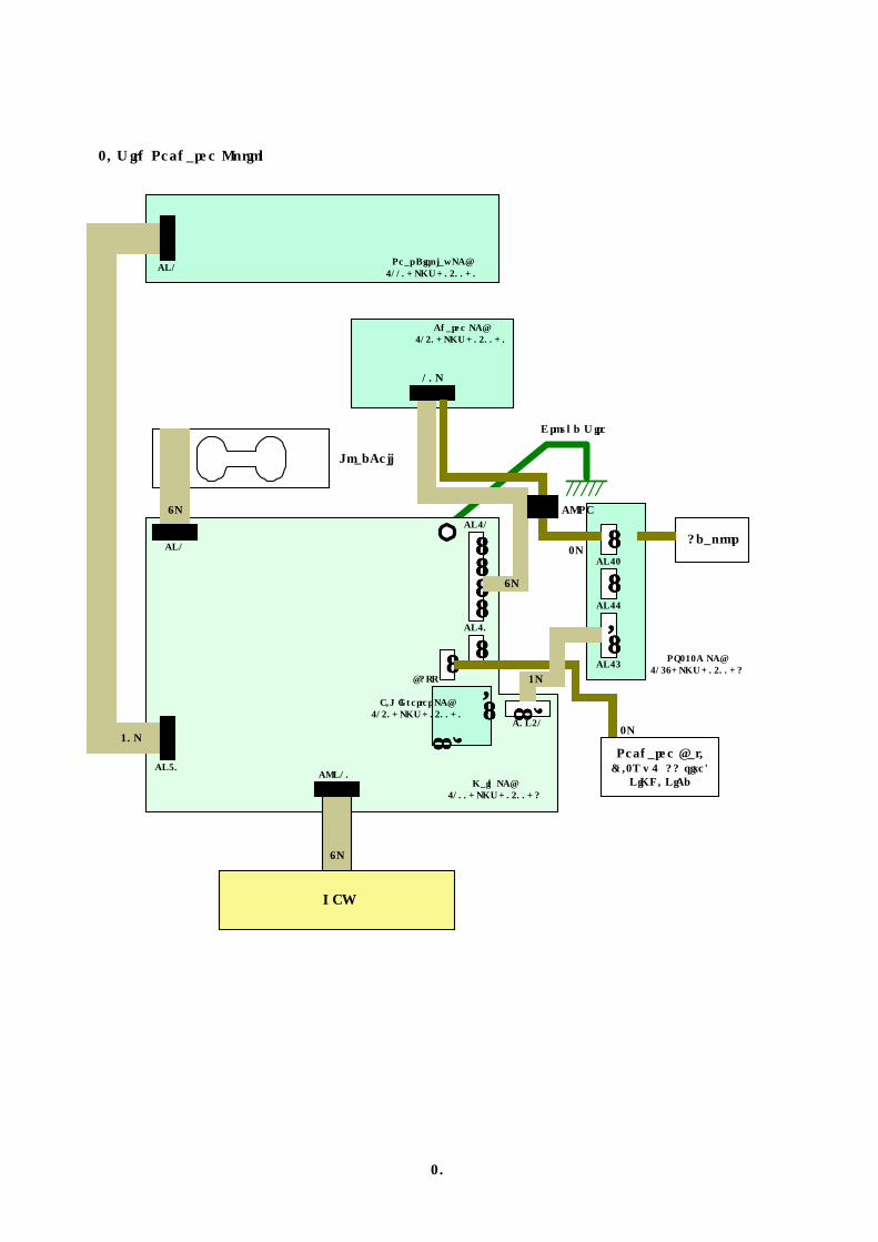
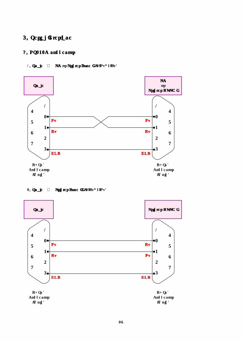
C. C. C. C. WiWiWiWiring ring ring ring DDDDiagramiagramiagramiagram
1. Without Recharge Option.
::::
::::
....::::
KEY
::::
::::::::::::::::
::::
... .::: :
Dry Bat.(1.5V x 6 AA size)
Main PCB6100-PMW-0400-A
RS232C PCB6158-PMW-0400-A
E.L Inverter PCB6140-PMW-0400-0
LoadCell
Rear Display PCB6110-PMW-0400-0
....::::
... .::: :
Adaptor
CN60
CN61
CN65
CN66
CN62
C0N41
BATT
CN1
CN70CON10
CN1
30P
8P
8P
Ground Wire
CORE
3P
2P
2P
20
2. With Recharge Option
::::
::::::::::::::::
::::
::::
::::
....::::
KEY
... .::: :
Recharge Bat.(1.2V x 6 AA size)
NiMH. NiCdMain PCB6100-PMW-0400-A
RS232C PCB6158-PMW-0400-A
E.L Inverter PCB6140-PMW-0400-0
LoadCell
Rear Display PCB6110-PMW-0400-0
....::::
... .::: :
Adaptor
CN60
CN61
CN65
CN66
CN62
C0N41
BATT
CN1
CN70CON10
CN1
30P
8P
8P
Ground Wire
Charge PCB6140-PMW-0400-0
8P
10P
3P
2P
2P
CORE
21
D. Parts LocationD. Parts LocationD. Parts LocationD. Parts Location
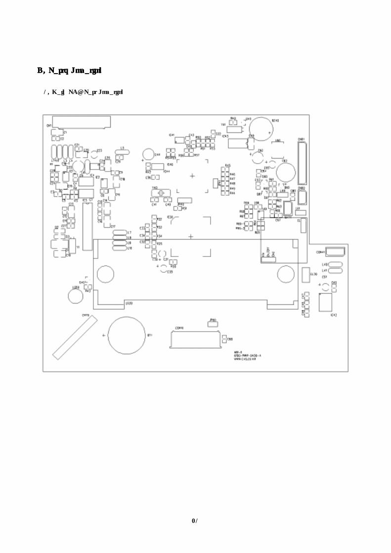
1. Main PCB Part Location
22
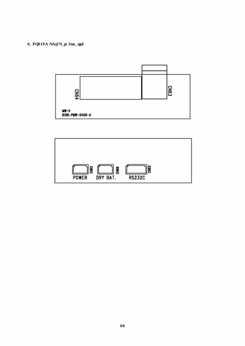
2. RS232C PCB Part Location
23
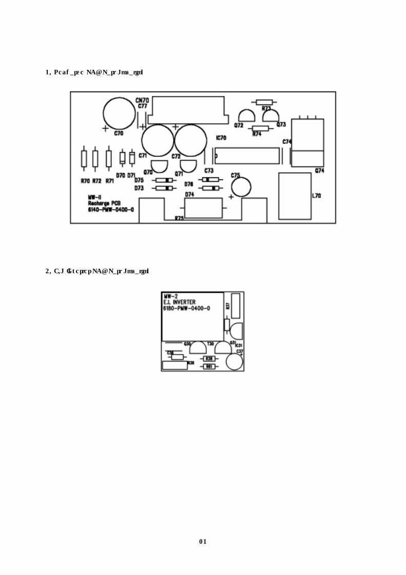
3. Recharge PCB Part Location
4. E.L Inverter PCB Part Location
24
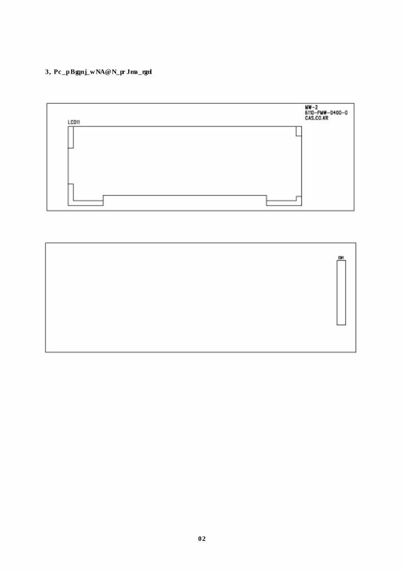
5. Rear Display PCB Part Location
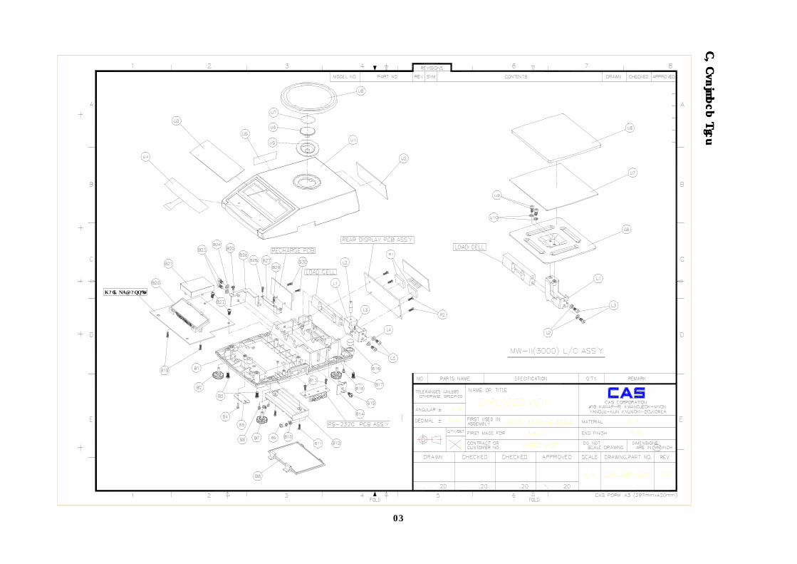
25
MAIN PCB ASS'Y
E. E
xploded View
E. E
xploded View
E. E
xploded View
E. E
xploded View
26
4. The Error Message4. The Error Message4. The Error Message4. The Error Message
A. Error MessageA. Error MessageA. Error MessageA. Error Message
ErrorErrorErrorError Reasons & SolutioReasons & SolutioReasons & SolutioReasons & Solutionsnsnsns NoteNoteNoteNote
CCCC AAAA L.L.L.L. EEEE rrrr - Span calibrate the scale, if this error is still
displayed, check EEPROM. Calibration Error
rrrr tttt c.c.c.c. EEEE rrrr - Check Real Time Clock. Real Time Clock
Error
OOOO LLLL ---- LLLL
- Check for platter or platform obstruction.
- Sample weight is lower than standard weight in
counting and percent mode.
※ Standard weight( MW-II 300 )
Counting mode : 2g
Percent mode : 5g
Underload Error
OOOO LLLL ---- HHHH - Remove all items from platter and turn on the
power. Overload Error
IIII nnnn iiii tttt ???? - If you want to initialize EEPROM, press the SET
key. EEPROM Initializing
LLLL AAAA cccc kkkk
- Minimum unit weight is lower than 0.005g when
you set sample in counting mode and percent
mode.
Lack Unit Weight
27
B. TroubleshootingB. TroubleshootingB. TroubleshootingB. Troubleshooting
1. 1. 1. 1. ““““CAL. ErCAL. ErCAL. ErCAL. Er””””
1) Go to calibration mode. CALCALCALCAL Switch is located in the battery cover at the bottom of the
scale. While pressing the switch, turn on the power then you will go to calibration mode.
2) Span calibrate the scale on ““““C.SPANC.SPANC.SPANC.SPAN””””menu. Refer to Span Calibration on page 6.
3) Press the MODEMODEMODEMODE key twice, the display shows ““““C.C.C.C.trim”trim”trim”trim”.
4) When the display shows ““““CCCC....trim”trim”trim”trim”, press the CALCALCALCAL switch and SET SET SET SET key.
5) The display shows AD value, this value is flickering because it is not filtered. If it is not
flickering, it means a failure of AD part.
6) Make sure that there is nothing on the platter and press the TARETARETARETARE key.
7) Place the weight of maximum capacity on the platter.
8) If the value is lower than 200.000, check the output of load cell. This value should be
greater than 200.000.
9) Turn the power off and on. You will go to normal mode. If the display shows ““““CAL. ErCAL. ErCAL. ErCAL. Er””””,
check EEPROM.
2. 2. 2. 2. ““““Init ?Init ?Init ?Init ?””””
1) If the display shows ““““ Init ? Init ? Init ? Init ?””””, press the SETSETSETSET key. If you press another key, EEPROM is
not initialized and go to next step.
2) ““““CAL.ErCAL.ErCAL.ErCAL.Er””””is displayed in 10 seconds.
3) Span calibrate the scale again. Turn the power off and on.
4) If the display shows still ““““Init ?Init ?Init ?Init ?””””, check EEPROM.
28
5. Serial Interface5. Serial Interface5. Serial Interface5. Serial Interface
A. RS232C connectorA. RS232C connectorA. RS232C connectorA. RS232C connector
1. ScaleScaleScaleScale ⇔ PCPCPCPC or Printer Type Printer Type Printer Type Printer Type IIII (2:Rx, 3:Tx)
16 27 38 49 5
1 62 73 84 95
RxRxRxRx
TxTxTxTx
GNDGNDGNDGND
RxRxRxRx
TxTxTxTx
GNDGNDGNDGND
D-SubConnector(9 pin)
D-SubConnector(9 pin)
ScaleScaleScaleScalePCPCPCPCor
Printer TYPE IPrinter TYPE IPrinter TYPE IPrinter TYPE I
2. ScaleScaleScaleScale ⇔ Printer Type Printer Type Printer Type Printer Type IIIIIIII (2:Tx, 3:Rx)
16 27 38 49 5
1 62 73 84 95
RxRxRxRx
TxTxTxTx
GNDGNDGNDGND
TxTxTxTx
RxRxRxRx
GNDGNDGNDGND
D-SubConnector(9 pin)
D-SubConnector(9 pin)
ScaleScaleScaleScale Printer TYPE IPrinter TYPE IPrinter TYPE IPrinter TYPE I
29
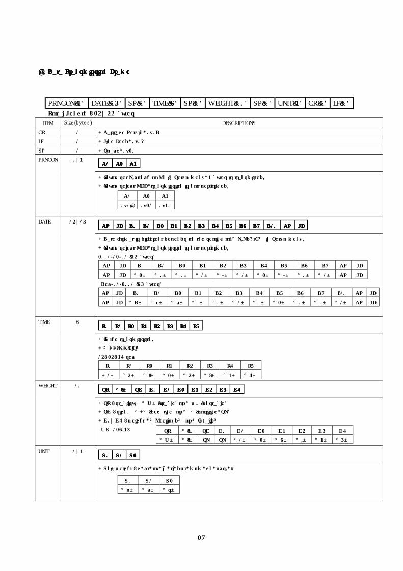
B. Data Transmission FramB. Data Transmission FramB. Data Transmission FramB. Data Transmission Frameeee
Total Length : 24~44 bytes
ITEM Size(bytes) DESCRIPTIONS
CR 1 - Carriage Return, 0x0D
LF 1 - Line Feed, 0x0A
SP 1 - Space, 0x20
C1C1C1C1 C2C2C2C2 C3C3C3C3 PRNCON 0~3
- If you set P.conch to On in Setup menu, 3 bytes is transmitted.
- If you select OFF, transmission is not performed.
C1 C2 C3
0x1B 0x21 0x30
CRCRCRCR LFLFLFLF D0D0D0D0 D1D1D1D1 D2D2D2D2 D3D3D3D3 D4D4D4D4 D5D5D5D5 D6D6D6D6 D7D7D7D7 D8D8D8D8 D9D9D9D9 D10D10D10D10 CRCRCRCR LFLFLFLF DATE 14~15
- Date format is different depends on the setting of “P.PdAtE” in Setup menu.
- If you select OFF, transmission is not performed.
2001/12/01 (14 bytes)
CR LF D0 D1 D2 D3 D4 D5 D6 D7 D8 D9 CR LF
CR LF ‘2’ ‘0’ ‘0’ ‘1’ ‘/’ ‘1’ ‘2’ ‘/’ ‘0’ ‘1’ CR LF
Dec/01/2001 (15 bytes)
CR LF D0 D1 D2 D3 D4 D5 D6 D7 D8 D9 D10 CR LF
CR LF ‘D’ ‘e’ ‘c’ ‘/’ ‘0’ ‘1’ ‘/’ ‘2’ ‘0’ ‘0’ ‘1’ CR LF
T0T0T0T0 T1T1T1T1 T2T2T2T2 T3T3T3T3 T4T4T4T4 T5T5T5T5 T6T6T6T6 T7T7T7T7 TIME 8
- In the transmission.
- “HH:MM:SS”
14: 24: 36 sec
T0 T1 T2 T3 T4 T5 T6 T7
’1’ ‘4’ ‘:’ ‘2’ ‘4’ ‘:’ ‘3’ ‘6’
STSTSTST ‘‘‘‘::::’’’’ SGSGSGSG G0G0G0G0 G1G1G1G1 G2G2G2G2 G3G3G3G3 G4G4G4G4 G5G5G5G5 G6G6G6G6 WEIGHT 10
- ST : stability. ‘W’(stable) or ‘w’(unstable)
- SG : sign. ‘-‘(negative) or ‘ ‘(positive, SP)
- G0~G6 : weight , “Overload” or “Invalid”
W: 128.35 ST ‘:’ SG G0 G1 G2 G3 G4 G5 G6
‘W’ ‘:’ SP SP ‘1’ ‘2’ ‘8’ ‘.’ ‘3’ ‘5’
U0U0U0U0 U1U1U1U1 U2U2U2U2 UNIT 1~3
- Unit weight : g, ct, oz, lb, tl, dwt, mom, gn, pcs., %
U0 U1 U2
‘p’ ‘c’ ‘s’
PRNCON(3) DATE(15) SP(1) TIME(8) SP(1) WEIGHT(10) SP(1) UNIT(3) CR(1) LF(1)

30
6. Parts list6. Parts list6. Parts list6. Parts list A. A. A. A. ELECTRONIC PARTELECTRONIC PARTELECTRONIC PARTELECTRONIC PARTSSSS
NO MAT'L NEW CODE PART NAME SPECIFICATION UNIT Q'TY LOCATION
MAIN PCB ASS'Y [ 240-M21-EMAP-UN01-01 ]
1 6100-PMW-0400-B MAIN PCB 6100-PMW-0400-B(MW-II) EA 1
2 6200-IS0-8951-A IC (CPU) P89C51RD2HBA EA 1 IC40
3 6205-IS0-9346-A IC(EEP-ROM) CAT93C46S(SMD) EA 1 IC41
4 6214-I00-5522-0 A/D CONVERTER CS5522-AP(MW-300) EA 1 IC3
5 6220-IS0-7805-0 IC(REGULATOR) KA7805(D-PACK) EA 1 U60
6 6224-I00-7225-0 IC(DRIVER) UPD 7225G00 EA 1 IC30
7 6228-I00-8563-0 IC(TIMMER) PCF8563P/F4 EA 1 IC43
8 6240-IS0-0062-0 IC(OP-AMP) NJM062-JRC EA 1 U61
9 6240-IS0-0177-0 IC(OP-AMP) OP-177GS EA 2 IC1,2
10 6240-IS0-0232-0 IC(LINE DRIVEER) ICL232CBE(SMD) EA 1 IC42
11 6242-IS0-7660-0 IC TC-7660ICL(S) EA 1 IC4
12 6271-I00-7180-0 SIDAC(VARISTOR) INR7D180 EA 5 RV1,2,3,4,5
13 6281-I00-1298-0 CHIP-TRANSISTOR KTA1298Y EA 2 Q60,40
14 6281-I00-2222-0 CHIP TRANSISTOR 2N2222AS EA 1 Q61
15 6294-ICP-0184-0 CHIP DIODE KDS184 EA 2 D40,60
16 6294-ISW-4148-A SWITCHING-DIODE PMLL4148L(LP-CONT') EA 3 D1,2,3
17 6527-ID3-0300-0 CHIP RE' 1/10W RR1220P-303D(30 ) EA 3 R64,67,31
18 6527-ID3-0499-0 CHIP RE' 1/10W RR1220P-4992D(49.9K) EA 4 R3,4,30,69-2
19 6527-IJ0-2200-0 CHIP RE' 1/10W FTR 0805 221 JR(220) EA 1 R70
20 6527-IJ3-0010-0 CHIP RE' 1/10W FTR 0805 102 JR(1K) EA 5 R32,50,51,52,53
21 6527-IJ3-0020-0 CHIP RE' 1/10W FTR 0805 202 JR(2K) EA 1 R61
22 6527-IJ3-0047-0 CHIP RE' 1/10W FTR 0805 472 JR(4.7K) EA 4 R54,55,56,57
23 6527-IJ3-0100-0 CHIP RE' 1/10W FTR 0805 103 JR(10K) EA 6 R43,40,60,33,34,35
24 6527-IJ3-0200-0 CHIP RE' 1/10W FTR 0805 203 JR(20K) EA 2 R65,71
25 6527-IJ3-0470-0 CHIP RE' 1/10W FTR 0805 473 JR(47K) EA 2 R68,69-1
26 6527-IJ3-1000-0 CHIP RE' 1/10W FTR 0805 104 JR(100K) EA 10 R44,45,46,47,48,49,62,63,66,
69
27 6540-LB3-1200-0 PRECISOIN RESISTOR FLBY 120K EA 2 R1,2
28 6670-T00-0470-0 INDUCTANCE 470μH EA 2 L60,61
29 6702-CAP-0106-0 CHIP TANTAL 10MCS 106 MB TER EA 12 C49,1,20,25,18-1,18,19,19-1,
13,14,10,17
30 6704-C25-0330-0 ELECTRIC-CONDENSER 330UF/25V EA 1 C62
31 6706-C16-0010-0 CHIP ELECTRIC CONDENSER 10uF/16V EA 5 C51,65,31,23,69
32 6706-C16-0100-0 CHIP ELECTRIC CONDENSER 100uF/16V Φ6.3 EA 2 C22,63
33 6706-C50-0001-0 CHIP ELECTRIC CONDENSER 1uF/50V Φ4.0 EA 1 C35
34 6712-CHP-0103-0 CHIP CONDENSER CL21F 103 KBNC EA 1 C11
35 6712-CHP-0104-0 CHIP CONDENSER CL21F 104 KBNC EA 32 C2,8,9,12,15,16,21,24,26,27,
28,29,30,32,33,34,36,42,
43,45,46,47,48,52,53,60,61,
64,66,67,68,
36 6712-CHP-0200-0 CHIP CONDENSER CL21C 200 JBNC(20PF) EA 2 C40,41

31
NO MAT'L NEW CODE PART NAME SPECIFICATION UNIT Q'TY LOCATION
37 6712-CHP-0300-0 CHIP CONDENSER CL21F 300 JBNC EA 1 C5
38 6720-CAP-0105-A POLYESTER-CONDENSER 1UF/63V-J(BOX) EA 2 C6,7
39 6800-F00-0220-0 EMI FILTER 220PF(TDK) EA 12 L1,2,3,4,5,6,7,8,9,10,40,41
40 7002-Z00-0070-0 PIEZO BUZZER EFM-250A EA 1 BZ40
41 7010-ZK0-3276-0 CRYSTAL 32.768KHZ EA 2 Y1,41
42 7010-ZM0-1105-A CRYSTAL 11.0592 MHZ(ATS-49/U) EA 1 Y40
43 7212-D00-9758-A LCD(MW-2) 9758A(TRANSFLECTIVE) EA 1 LD30
44 7520-P00-2032-A BATTERY CR2032-3V(PIN TYPE) EA 1 BT1
45 7600-STA-1902-0 TACT S/W 11902(DJTA-1102) EA 1 SW41
46 7805-CCN-6702-0 CONNECTOR(WAFER) 5267-02 EA 1 CN67
47 7805-CCN-6703-0 CONNECTOR(WAFER) 5267-03 EA 1 CN41
48 7805-CCN-6708-0 CONNECTOR(WAFER) 5267-08 EA 1 CN61
49 7807-CFP-0008-0 FPC-CONNECTOR FCZ254-8S EA 1 CN1
50 7807-CFP-0008-A FPC-CONNECTOR FCZ254-8R EA 1 CON10
51 7821-CJM-0002-0 JUMPER 2PIN SET 1 JP41
52 7821-CJM-0003-0 JUMPER 3PIN SET 1 JP40
53 7806-YDA-0030-0 CONNECTOR(WAFER) YDAW200-30(MW-2) EA 1 Option(Option(Option(Option(DDDD))))
54 7222-D00-0001-0 EL BACK LIGHT SPEL-01-001H(MW-2) EA 1 Option(B)Option(B)Option(B)Option(B)
55 7232-DRG-0004-0 LED LAMP Φ5-(R,G) BL-BVT 204(ANODE) EA 1 Option(R)Option(R)Option(R)Option(R)
56 2090-H00-0007-0 LED HOLDER 10mm*6mm*5mm(MW-2) EA 1 Option(R)Option(R)Option(R)Option(R)
RS232C PCB ASS'Y [ 240-M21-ERSP-UN01-01 ]
1 6158-PMW-0400-B RS232C PCB 6158-PMW-0400-B(MW-II) EA 1
2 7610-STA-0302-0 ADAPTOR JACK HS-302 EA 1 CN63
3 7805-CCN-6703-0 CONNECTOR(WAFER) 5267-03 EA 1 CN65
4 7805-CCN-6704-0 CONNECTOR(WAFER) 5267-04 EA 1 CN66
5 7812-C00-0009-B D-SUB CONNECTOR RD9S EA 1 CN64
6 7840-W00-0905-0 CONNECTOR WIRE 3P*3P*50mm(MW-2) EA 1
POWER ASS'Y [ 240-M21-EPWP-UN01-01 ]
1 7840-W00-1216-0 CONNECTOR WIRE 8P*4P*160mm-CORE(MW-2) EA 1
7840-W00-2221-0 CONNECTOR WIRE 10P*8P*4P*210mm-CORE EA 1 Option(R)Option(R)Option(R)Option(R)
2 7860-GND-0210-0 GROUND WIRE 1P*210mm(MW-2) EA 1
3 7860-GND-0040-0 GROUND WIRE 1P*40mm(MW-2) EA 1
E.L INVERTER PCB ASS'Y [ 240-M25-EELP-UN01-01 ] Option(B)Option(B)Option(B)Option(B)
1 6180-PMW-0400-0 E.L INVERTER PCB 6180-PMW-0400-0 EA 1
2 6220-I00-1350-0 IC(REGULATOR) S-81350 HG EA 1 IC31
3 6280-I00-1266-0 TRANSISTOR 2SA1266 EA 1 Q30
4 6280-I00-1815-0 TRANSISTOR 2SC1815A (3198) EA 1 Q31
5 6506-MF3-0010-0 RESISTOR 1/8W MFR 1K (±1%)-F EA 1 R61
6 6506-MF3-0100-0 RESISTOR 1/8W MFR 10K (±1%)-F EA 1 R36
7 6506-MF3-1000-0 RESISTOR 1/8W MFR 100K (±1%)-F EA 2 R37,38
8 6704-C25-0100-0 ELECTRIC-CONDENSER 100UF/25V EA 1 C37

32
NO MAT'L NEW CODE PART NAME SPECIFICATION UNIT Q'TY LOCATION
9 6710-CAP-0104-0 CERAMIC-CONDENSER 0.1UF/25V(50V) EA 1 C36
10 7244-D00-0005-0 E.L INVERTER SPEL-I-5C(NC,BI,CI-2001B) EA 1 T30
11 7810-C00-9295-0 CONNECTOR FW0254-30 EA 0.2
RECHARGE PCB ASS'Y [ 240-M25-ERCP-UN01-01 ] Option(R)Option(R)Option(R)Option(R)
1 6140-PMW-0400-0 RECHARGE PCB 6140-PMW-0400-0 EA 1
2 6232-I00-0713-0 IC MAX713CPE EA 1 IC70
3 6273-I00-9530-0 MOSFET IRF9530 EA 1 Q74
4 6280-I00-1266-0 TRANSISTOR 2SA1266 EA 1 Q73
5 6280-I00-1815-0 TRANSISTOR 2SC1815A (3198) EA 2 Q70,71
6 6280-I00-1959-0 TRANSISTOR 2SC1959 EA 1 Q72
7 6291-IPO-5819-0 POWER DIODE 1N5819 EA 4 D73,74,75,76
8 6294-ISW-4148-0 SWITCHING-DIODE 1N4148P EA 2 D70,71
9 6505-MB0-0500-0 RESISTOR 1/4W MFR 50Ω(±0.1%)-B EA 2 R71,73
10 6512-CJ0-0006-6 RESISTOR 2W CFR 0.66Ω (±5%) EA 1 R75
11 6515-CJ3-0010-0 RESISTOR 1/4W CFR 1K (±5%) EA 1 R74
12 6515-CJ3-0020-0 RESISTOR 1/4W CFR 2K (±5%) EA 1 R70
13 6515-CJ3-1000-0 RESISTOR 1/4W CFR 100K (±5%) EA 1 R72
14 6670-T00-0220-0 INDUCTANCE 220uH EA 1 L70
15 6704-C16-0100-0 ELECTRIC-CONDENSER 100uF/16V EA 1 C75
16 6704-C25-0330-0 ELECTRIC-CONDENSER 330UF/25V EA 3 C70,71,76
17 6704-C25-0470-0 ELECTRIC-CONDENSER 470uF/25V EA 1 C72
18 6710-CAP-0104-0 CERAMIC-CONDENSER 0.1UF/25V(50V) EA 1 C77
19 6710-CAP-P221-0 CERAMIC-CONDENSER 220PF/50V EA 1 C74
20 6720-CAP-0104-A POLYESTER-CONDENSER 0.1UF/63V-J(BOX) EA 1 C73
21 7809-CAL-0010-0 CONNECTOR(WAFER) LAL 0640-10 EA 1 CN70
REAR DISPLAY PCB ASS'Y [ 240-M24-ERDP-UN01-01 ] Option(D)Option(D)Option(D)Option(D)
1 2631-A00-0002-0 VFD CUSHION 30*20*6T EA 2
2 6110-PMW-0400-A DISPLAY PCB 6110-PMW-0400-A EA 1
3 7212-D00-9758-0 LCD 9758A-R/F(MW-II) EA 1 LCD11
4 7806-YDW-0030-0 CONNECTOR(WAFER) YDW200-30(MW-2) EA 1 CN1
5 7830-W00-3023-0 REAR DISPLAY WIRE 30P*30P*230(MW-2) EA 1

33
B. B. B. B. MECHANICAL PARTMECHANICAL PARTMECHANICAL PARTMECHANICAL PART
MODEL : MW-II(300) REV:01
NO MAT'L NEW CODE PART NAME SPECIFICATION UNIT Q'TY LOCATION
ASS'Y UPPER COVER (240-M21-MUPC-UN01-01)
1 2000-A00-0100-0 UPPER COVER ABS 750 190*291*55 EA 1
2000-A00-0117-0 UPPER COVER ABS 750 190*291*55(CE용) EA 1 CECECECE
2 2050-MW2-0000-0 DISPLAY COVER MW-II (후면) EA 1
2050-MW2-0333-5 DISPLAY COVER MW-II (300g) 영공 REAR EA 1 Option(D)Option(D)Option(D)Option(D)
3 2050-MW2-0333-4 DISPLAY COVER MW-II (300g) 영공 EA 1
2050-MW2-0333-5 DISPLAY COVER MW-II (300g) 영공 충전 EA 1 Option(Option(Option(Option(RRRR))))
4 2100-MW2-0000-0 MEMBRANE S/W LEXAN MW-II EA 1
5 1810-MW0-0033-2 SPEC PLATE MW-120,1200,II 공용 영공 EA 1
6 1210-A00-0020-0 PLATFORM Φ35*Φ10*15 EA 1
7 2631-A00-0021-A DOUBLE TAPE Φ34 EA 1
8 1000-A00-0115-0 TRAY Φ130*0.5t EA 1
9 2000-A00-0108-0 L/C HOLE COVER Φ59*Φ39.6*11.5 EA 1
10 1590-A00-0036-0 CONDUCTIVE SPRING Φ12*Φ8*4*0.3t EA 1
ASS'Y L/C BRACKET (240-M21-MLCB-UN01-01)
1 1050-A00-0038-0 L/C BRACKET AL 1.2t,61*22*36 EA 1
2 1210-A00-0089-0 LOAD SHAFT AL Φ7.3*19 EA 1
3 1501-A00-0306-0 MACHINE SCREW(FH) M3*6 EA 1
4 1551-MSU-0500-0 WASHER(SPR) Φ5-SUS EA 2
5 1530-MSU-0510-0 WRENCH BOLT M5*10-SUS EA 2
ASS'Y BODY (240-M21-MBOD-UN01-01)
1 2000-A00-0099-A BODY ABS750 190*291*45 EA 1
2000-A00-0118-0 BODY ABS750 190*291*45(CE용) EA 1 CECECECE
2 2008-A00-0002-0 FOOT PVC 25*6 EA 4
3 1502-A00-0408-0 MACHINE SCREW(PH) M4*8 EA 2
4 1265-A00-0001-0 SEALING BOLT M3*0.5*5(BsBn) EA 1
5 1000-A00-0202-0 SEALING PLATE SUS 42*17*1t EA 1
6 1590-A00-0032-0 BATTERY SPRING-A φ9*φ0.6*3 (MW-II) EA 1
7 1590-A00-0033-0 BATTERY SPRING-B φ9*φ0.6*6*3 (MW-II) EA 1
8 2000-A00-0101-0 BATTERY COVER ABS750 119.6*75.6*2t EA 1
9 1590-A00-0034-0 BATTERY SPRING-C φ9*φ0.6*3*6 (MW-II) EA 1
10 1590-A00-0035-0 BATTERY SPRING-D φ9*φ0.6*6 (MW-II) EA 1
11 1512-A00-0306-0 TAPPING SCREW(PH)-2 3*6 EA 2
12 2013-A00-0005-A BATTERY HOLDER HDPE EA 1
13 1512-A00-0310-0 TAPPING SCREW(PH)-2 3*10 EA 2
14 1030-A00-0148-0 LIMIT BRACKET SPC 1.5t, 30*14*15 EA 1
15 1503-A00-0512-0 MACHINE SCREW(WPH) M5*12 EA 1
16 1503-MPN-0310-0 MACHINE SCREW(WPH) M3*10 EA 1
17 1512-A00-0420-0 TAPPING SCREW(PH)-2 4*20 EA 2
18 2022-A00-0005-0 W/L GAUGE Φ15*8(RED) EA 1

34
NO MAT'L NEW CODE PART NAME SPECIFICATION UNIT Q'TY LOCATION
19 1512-A00-0310-0 TAPPING SCREW(PH)-2 3*10 EA 2
20 2000-A00-0107-A LCD BRACKET ABS750 EA 1
21 1040-A00-0006-0 SHIELD CASE SPTE 0.5t,63*45*13.5 EA 1
22 1512-A00-0412-0 TAPPING SCREW(PH)-2 4*12 EA 2
23 1530-MSU-0515-0 WRENCH BOLT(WPH) M5*15 EA 2
24 1503-MPN-0304-0 MACHINE SCREW(WPH) M3*4 EA 1
25 1030-A00-0150-0 L/C PLATE SPC 2t EA 1
26 1030-A00-0152-0 PCB BRACKET SPC 1t EA 1
27 1502-A00-0305-0 MACHINE SCREW M3*5 EA 1
28 1512-A00-0310-0 TAPPING SCREW(PH)-2 3*10 EA 1
29 1503-A00-0310-0 MACHINE SCREW M3*10 EA 2
30 7840-W00-0224-0 CONNECTOR WIRE 2P*70*170(MW-II) EA 1
31 2631-A00-0023-0 BATTERY COVER CUSHION 80*26*2t(EVA) EA 1
ASS'Y C/T BOX (240-M21-MCTB-UN01-01)
1 7510-P12-1122-0 AC ADATOR 110/220-12V/300mA EA 1
7510-P12-1122-G AC ADATOR 110/220-12V/850mA EA 1 Option(R) Option(R) Option(R) Option(R)
7510-P12-0220-H AC ADATOR 220V 12V/850mA EA 1 CECECECE
2 9100-MW2-0100-0 C/T BOX-1 MW-2 EA 1
3 9202-APE-0003-0 POLY ETHYLENE PAD 268*200*110 EA 1
4 9203-APE-0001-0 POLY ETHYLENE BOX 345*208 EA 2
5 9310-A00-0003-0 MANUAL POLY BAG 170*250*0.05t EA 1
6 9302-A00-0003-0 TRAY POLY BAG 200*250*0.05t EA 1
7 9302-A00-0005-A SET POLY BAG 270*350*0.04t EA 1
8 9400-A00-0046-0 SILICAGEL 10g EA 2
9 7520-P00-0170-0 NI-MH BATTERY GP130AAHC(1.2V) EA 6 Option(R) Option(R) Option(R) Option(R)
LOAD CELL ASS'Y (LLA-BMW-301G-0000-0N) MW-2 L/C(200/300g) EA 1

35
MODEL : MW-II(3000) REV:01
NO MAT'L NEW CODE PART NAME SPECIFICATION UNIT Q'TY LOCATION
ASS'Y UPPER COVER (240-M23-MUPC-UN01-01)
1 2000-A00-0100-0 UPPER COVER ABS 750 190*291*55 EA 1
2000-A00-0117-0 UPPER COVER ABS 750 190*291*55(CE용) EA 1 CECECECE
2 2050-MW2-0000-0 DISPLAY COVER MW-II (후면) EA 1
2050-MW2-3033-5 DISPLAY COVER MW-II (3kg) 영공 REAR EA 1 Option(D)Option(D)Option(D)Option(D)
3 2050-MW2-3033-4 DISPLAY COVER MW-II (3kg) 영공 EA 1
2050-MW2-3033-6 DISPLAY COVER MW-II (3kg) 영공 충전 EA 1 Option(Option(Option(Option(RRRR))))
4 2100-MW2-0000-0 MEMBRANE S/W LEXAN MW-II EA 1
5 1810-MW0-0033-2 SPEC PLATE MW-120,1200,II 공용 영공 EA 1
6 1000-A00-0203-0 TRAY SUS 0.5t,158*145*0.5t EA 1
7 1050-A00-0039-0 PLATFORM AL 2t,156*143 EA 1
ASS'Y L/C BRACKET (240-M23-MLCB-UN01-01)
1 1030-A00-0147-0 L/C BRACKET SPC 2t,65*24*53 EA 1
2 1551-MSU-0500-0 WASHER(SPR) Φ5-SUS EA 2
3 1530-MSU-0510-0 WRENCH BOLT M5*10-SUS EA 2
ASS'Y BODY (240-M21-MBOD-UN01-01)
1 2000-A00-0099-A BODY ABS750 190*291*45 EA 1
2000-A00-0118-0 BODY ABS750 190*291*45(CE용) EA 1 CECECECE
2 2008-A00-0002-0 FOOT PVC 25*6 EA 4
3 1502-A00-0408-0 MACHINE SCREW(PH) M4*8 EA 2
4 1265-A00-0001-0 SEALING BOLT M3*0.5*5(BsBn) EA 1
5 1000-A00-0202-0 SEALING PLATE SUS 42*17*1t EA 1
6 1590-A00-0032-0 BATTERY SPRING-A φ9*φ0.6*3 (MW-II) EA 1
7 1590-A00-0033-0 BATTERY SPRING-B φ9*φ0.6*6*3 (MW-II) EA 1
8 2000-A00-0101-0 BATTERY COVER ABS750 119.6*75.6*2t EA 1
9 1590-A00-0034-0 BATTERY SPRING-C φ9*φ0.6*3*6 (MW-II) EA 1
10 1590-A00-0035-0 BATTERY SPRING-D φ9*φ0.6*6 (MW-II) EA 1
11 1512-A00-0306-0 TAPPING SCREW(PH)-2 3*6 EA 2
12 2013-A00-0005-A BATTERY HOLDER HDPE EA 1
13 1512-A00-0310-0 TAPPING SCREW(PH)-2 3*10 EA 2
14 1030-A00-0148-0 LIMIT BRACKET SPC 1.5t, 30*14*15 EA 1
15 1503-A00-0512-0 MACHINE SCREW(WPH) M5*12 EA 1
16 1503-MPN-0310-0 MACHINE SCREW(WPH) M3*10 EA 1
17 1512-A00-0420-0 TAPPING SCREW(PH)-2 4*20 EA 2
18 2022-A00-0005-0 W/L GAUGE Φ15*8(RED) EA 1
19 1512-A00-0310-0 TAPPING SCREW(PH)-2 3*10 EA 2
20 2000-A00-0107-A LCD BRACKET ABS750 EA 1
21 1040-A00-0006-0 SHIELD CASE SPTE 0.5t,63*45*13.5 EA 1
22 1512-A00-0412-0 TAPPING SCREW(PH)-2 4*12 EA 2
23 1530-MSU-0515-0 WRENCH BOLT(WPH) M5*15 EA 2
24 1503-MPN-0304-0 MACHINE SCREW(WPH) M3*4 EA 1
25 1030-A00-0150-0 L/C PLATE SPC 2t EA 1
26 1030-A00-0152-0 PCB BRACKET SPC 1t EA 1

36
NO MAT'L NEW CODE PART NAME SPECIFICATION UNIT Q'TY LOCATION
27 1502-A00-0305-0 MACHINE SCREW M3*5 EA 1
28 1512-A00-0310-0 TAPPING SCREW(PH)-2 3*10 EA 1
29 1503-A00-0310-0 MACHINE SCREW M3*10 EA 2
30 7840-W00-0224-0 CONNECTOR WIRE 2P*70*170(MW-II) EA 1
31 2631-A00-0023-0 BATTERY COVER CUSHION 80*26*2t(EVA) EA 1
ASS'Y C/T BOX (240-M21-MCTB-UN01-01)
1 7510-P12-1122-0 AC ADATOR 110/220-12V/300mA EA 1
7510-P12-1122-G AC ADATOR 110/220-12V/850mA EA 1 Option(R) Option(R) Option(R) Option(R)
7510-P12-0220-H AC ADATOR 220V 12V/850mA EA 1 CECECECE
2 9100-MW2-0100-0 C/T BOX-1 MW-2 EA 1
3 9202-APE-0003-0 POLY ETHYLENE PAD 268*200*110 EA 1
4 9203-APE-0001-0 POLY ETHYLENE BOX 345*208 EA 2
5 9310-A00-0003-0 MANUAL POLY BAG 170*250*0.05t EA 1
6 9302-A00-0003-0 TRAY POLY BAG 200*250*0.05t EA 1
7 9302-A00-0005-A SET POLY BAG 270*350*0.04t EA 1
8 9400-A00-0046-0 SILICAGEL 10g EA 2
9 7520-P00-0170-0 NI-MH BATTERY GP130AAHC(1.2V) EA 6 Option(R) Option(R) Option(R) Option(R)
LOAD CELL ASS'Y (LLA-BMW-302G-0000-0N) MWN L/C(2kg/3kg) EA 1