Embed Size (px)
Citation preview
1
SERVICE MANUAL BE-3E CHASSISMODEL COMMANDER DEST CHASSIS NO. MODEL COMMANDER DEST CHASSIS NO.
KV-32FX20A RM-887 Italian SCC-Q22B-A
KV-32FX20B RM-887 French SCC-Q23B-A
KV-32FX20D RM-887 AEP SCC-Q21B-A
KV-32FX20E RM-887 Spanish SCC-Q24B-A
KV-32FX20U RM-887 UK SCC-Q25B-A
®M I C R O F I L M
TRINITRON ® COLOR TV
2
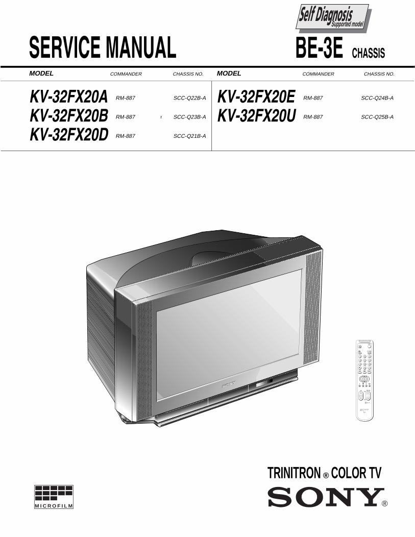
ITEM MODEL Television System Stereo System Channel Coverage Color System
Italian B/G/H GERMAN StereoITALIA VHF : A-H2 (C) UHF : 21-69 PALB/G/H VHF : E2-E12 UHF : E21-E69CABLE TV (1) : S1-S41CABLE TV (2) : S01-S05,M1-M10,U1-U10
PAL, SECAMNTSC4.43, NTSC3.58(VIDEO IN)
FrenchB/G/H, D/K,L,I GERMAN/NICAM
Stereo
L VHF : F02-F10 UHF : F21-F60CABLE : B-Q B/G/H VHF : E2-E12UHF : E21-E69CABLE TV (1) : S1-S41CABLE TV (2) : S01-S05, M1-M10, U1-U10ITALIA VHF : A-H2 (C) UHF : 21-69I UHF : B21-B69
PAL, SECAMNTSC4.43, NTSC3.58(VIDEO IN)
AEP B/G/H GERMAN StereoPAL B/G/H/ VHF : E2-E12 : E21-E69CABLE TV (1) : S1-S41CABLE TV (2) : S01-S05, M1-M10, U1-U10ITALIA VHF : A-H2 (C) UHF : 21-69
PAL, SECAMNTSC4.43, NTSC3.58(VIDEO IN)
Spanish B/G/H, D/K GERMAN/NICAM Stereo
PAL B/G/H/ VHF : E2-E12 : E21-E69CABLE TV (1) : S1-S41CABLE TV (2) : S01-S05, M1-M10, U1-U10ITALIA VHF : A-H2 (C) UHF : 21-69
PAL, SECAMNTSC4.43, NTSC3.58(VIDEO IN)
UK I NICAM Stereo UHF : B21-B69PALNTSC4.43, NTSC3.58(VIDEO IN)
MODEL 32FX20A 32FX20B 32FX20D 32FX20E 32FX20U
Power Consumption 106W 120W 120W 120W 176W
[PICTURE TUBE] FD Trinitron WideApprox. 82 cm (32 inches)(Approx. 76 cm picture measureddiagonally)102 degree deflection
Input/Output Terminals
[REAR]
1 21-pin Euro connector (CENELEC standard).
- Inputs for Audio and Video signals.- Inputs for RGB.- Outputs of TV Video and Audio signals.
2/ 2 21-pin Euro connector
- Inputs for Audio and Video signals.- Inputs for S video.- Outputs for Video and Audio signals (selectable).
Phono jacks
- Outputs for Audio Signals
[FRONT]
3 Video output - phono jack
3 Audio inputs - phono jacks
S Video input - 4 pin din
Headphone jack : stereo minijack
Sound output 2x20W (Music Power)Subwoofer 20W (Music Power)Power requirements 220 - 240V
Dimensions Approx 874x563x571mm (w/h/d)
Weight Approx 62kg
Supplied accessories RM-887 Remote Commander (1)IEC designated R6 batteries (2)
Other features NICAM*, FASTEXT, TOPTEXT * (KV-32FX20B, 32FX20E, 32FX20U)
[RM-887]Remote control system Infrared controlPower requirements 3V dc
2 batteries IEC designationR6 (size AA)
Dimensions Approx 44x209x23mm (w/h/d)Weight Approx 89g (Not including battery)
Design and specifications are subject to change without notice.
3
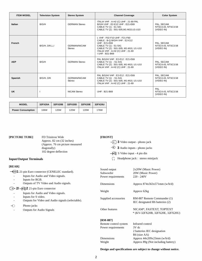
WARNING (KV-32FX20U only)
The flexible mains lead is supplied connected to a B.S. 1363 fused plughaving a fuse of 5 AMP capacity. Should the fuse need to be replaced,use a 5 AMP FUSE approved by ASTA to BS 1362, ie one that carries the mark.IF THE PLUG SUPPLIED WITH THIS APPLIANCE IS NOT SUITABLEFOR THE OUTLET SOCKETS IN YOUR HOME, IT SHOULD BE CUTOFF AND AN APPROPRIATE PLUG FITTED. THE PLUG SEVERED FROM THE MAINS LEAD MUST BE DESTROYED AS A PLUG WITH BARED WIRES IS DANGEROUS IF ENGAGED IN A LIVE OUTLET SOCKET.When an alternative type of plug is used it should be fitted with a 5 AMPFUSE, otherwise the circuit should be protected by a 5 AMP FUSE at the distribution board.
ASAT
Model Name
Item
KV-32FX20A KV-32FX20B KV-32FX20D KV-32FX20E KV-32FX20U
Pal Comb OFF OFF OFF OFF OFF
PIP OFF OFF OFF OFF OFF
RGB Priority OFF OFF OFF OFF OFF
Woofer Box ON ON ON ON ON
Scart 1 ON ON ON ON ON
Scart 2 ON ON ON ON ON
Front in (3) ON ON ON ON ON
Scart 4 OFF OFF OFF OFF OFF
Projector OFF OFF OFF OFF OFF
AKB in 16:9 mode ON ON ON ON ON
Norm B/G ON ON ON ON OFF
Norm I OFF ON OFF OFF ON
Norm D/K OFF ON OFF ON OFF
Norm AUS OFF OFF OFF OFF OFF
Norm L OFF ON OFF OFF OFF
Norm SAT OFF OFF OFF OFF OFF
Norm M OFF OFF OFF OFF OFF
Teletext ON ON ON ON ON
Nicam Stereo OFF ON OFF ON ON
Language Preset Italian French German Spanish English
How to replace the fuse.Open the fuse compartment witha screwdriver blade and replacethe fuse.
FUSE
4
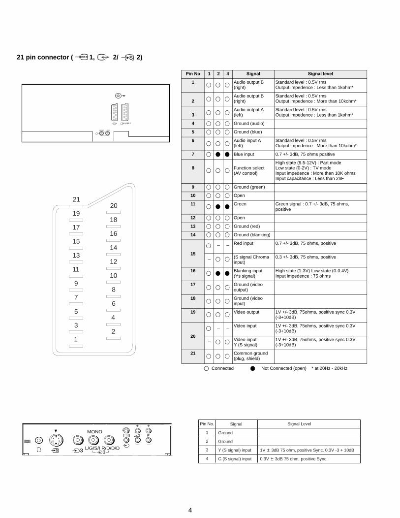
21 pin connector ( 1, 2/ 2)
Connected Not Connected (open) * at 20Hz - 20kHz
19
17
15
13
11
9
7
5
3
1
20
18
16
14
12
10
8
6
4
2
21
Pin No 1 2 4 Signal Signal level
1 Audio output B(right)
Standard level : 0.5V rmsOutput impedence : Less than 1kohm*
2Audio output B(right)
Standard level : 0.5V rmsOutput impedence : More than 10kohm*
3Audio output A(left)
Standard level : 0.5V rmsOutput impedence : Less than 1kohm*
4 Ground (audio)
5 Ground (blue)
6 Audio input A(left)
Standard level : 0.5V rmsOutput impedence : More than 10kohm*
7 Blue input 0.7 +/- 3dB, 75 ohms positive
8 Function select(AV control)
High state (9.5-12V) : Part mode Low state (0-2V) : TV modeInput impedence : More than 10K ohmsInput capacitance : Less than 2nF
9 Ground (green)
10 Open
11 Green Green signal : 0.7 +/- 3dB, 75 ohms, positive
12 Open
13 Ground (red)
14 Ground (blanking)
15
_ _ Red input 0.7 +/- 3dB, 75 ohms, positive
_ (S signal Chroma input)
0.3 +/- 3dB, 75 ohms, positive
16 Blanking input(Ys signal)
High state (1-3V) Low state (0-0.4V)Input impedence : 75 ohms
17 Ground (video output)
18 Ground (video input)
19 Video output 1V +/- 3dB, 75ohms, positive sync 0.3V(-3+10dB)
20
_ _ Video input 1V +/- 3dB, 75ohms, positive sync 0.3V(-3+10dB)
_ Video inputY (S signal)
1V +/- 3dB, 75ohms, positive sync 0.3V(-3+10dB)
21 Common ground(plug, shield)
Signal
Ground
Ground
Y (S signal) input
C (S signal) input
Pin No.
1
2
3
4
Signal Level
1V 3dB 75 ohm, positive Sync. 0.3V -3 + 10dB
0.3V 3dB 75 ohm, positive Sync.
L/G/S/I R/D/D/D
MONO+ +
P
_ _
s 3 3
R/D/D/D L/G/S/I
1 S 22
TABLE OF CONTENTS
Section Title Page Section Title Page
Warning and Caution .....................3Self-Diagnostic Function .....................6
1. GENERAL
Overview of the Remote .....................10Control ButtonsAdjusting the Picture .....................12Adjusting the Sound .....................12Teletext .....................13Troubleshooting .....................14
2. DISASSEMBLY
2-1. Rear Cover Removal .....................152-2. Chassis Assy Removal .....................152-3-1. Service Position (1) .....................152-3-2. Service Position (2) .....................152-4. Wire Dressing .....................162-5. A Board Removal .....................162-6. A Extension Board .....................162-7. Picture Tube Removal .....................17 Removal and Replacement of the .....................18
Main - Bracket Bottom Plates
3. SET-UP ADJUSTMENTS
3-1. Beam Landing .....................193-2. Convergence ..................... 20 3-3. Screen G2 .....................223-4. Focus .....................223-5. White Balance .....................23
5
CAUTION
SHORT CIRCUIT THE ANODE OF THE PICTURE TUBE AND THEANODE CAP TO THE METAL CHASSIS, CRT SHIELD, OR THECARBON PAINTED ON THE CRT, AFTER REMOVAL OF THEANODE CAP
WARNING !!
AN ISOLATING TRANSFORMER SHOULD BE USED DURING ANYSERVICE WORK TO AVOID POSSIBLE SHOCK HAZARD DUE TOLIVE CHASSIS. THE CHASSIS OF THIS RECEIVER IS DIRECTLYCONNECTED TO THE POWER LINE.
SAFETY-RELATED COMPONENT WARNING !!
COMPONENTS IDENTIFIED BY SHADING AND MARKED ONTHE SCHEMATIC DIAGRAMS, EXPLODED VIEWS AND IN THEPARTS LIST ARE CRITICAL FOR SAFE OPERATION. REPLACETHESE COMPONENTS WITH SONY PARTS WHOSE PART NUMBERSAPPEAR AS SHOWN IN THIS MANUAL OR IN SUPPLEMENTS PUBLISHED BY SONY.
ATTENTION
4. CIRCUIT ADJUSTMENTS
4-1. Electrical Adjustments .....................244-2. ‘TT’ Test Mode .....................274-3. ‘T’ Test Mode .....................28
5. DIAGRAMS
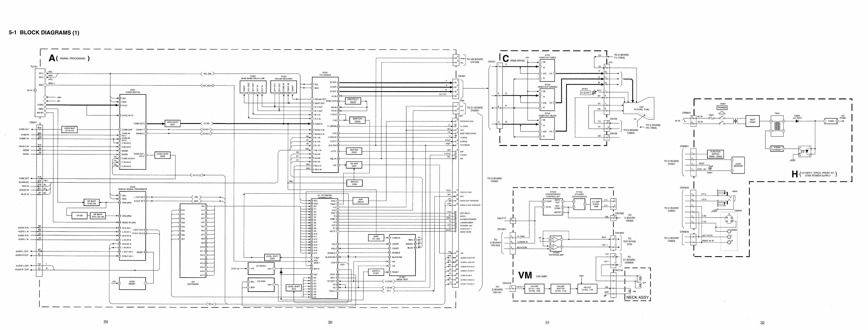
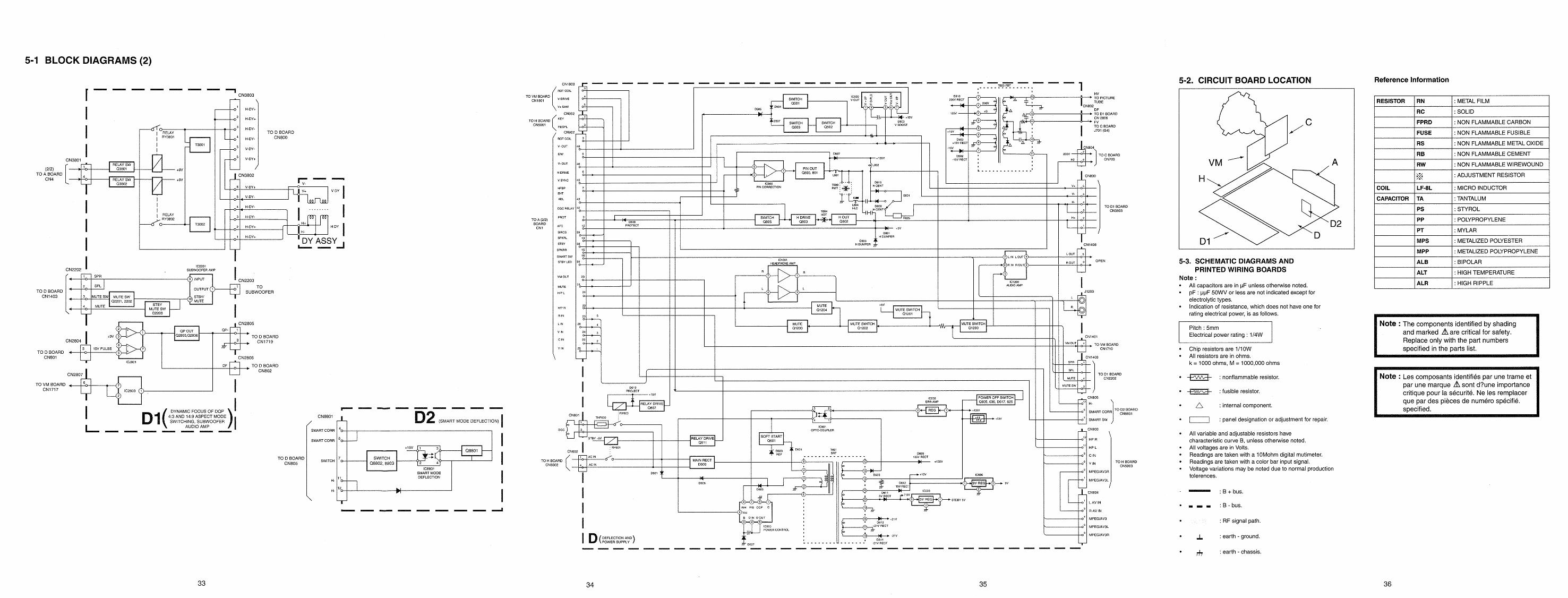
5-1. Block Diagrams (1) .....................29Block Diagrams (2) .....................33
5-2. Circuit Board Location .....................365-3. Schematic Diagrams and
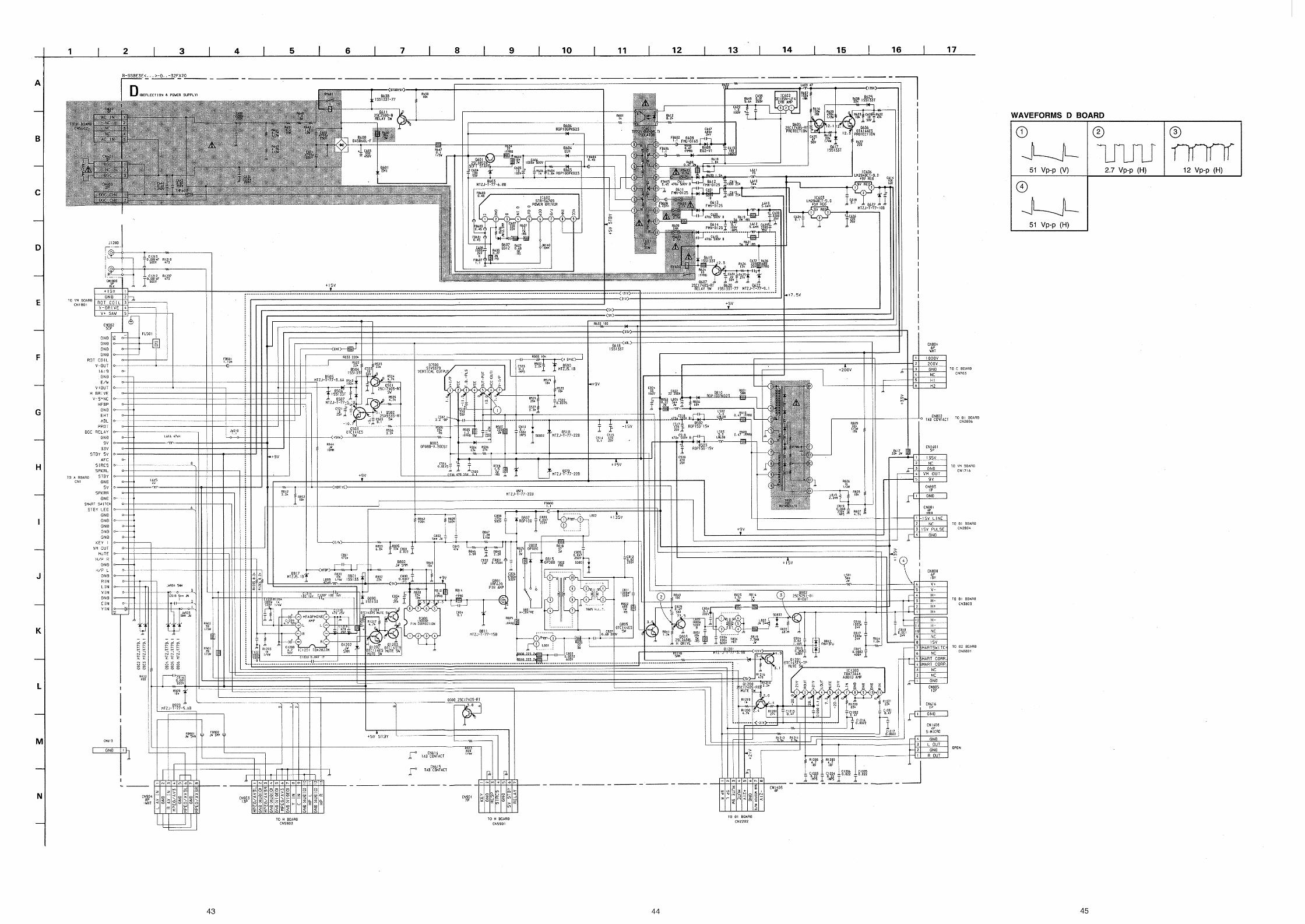
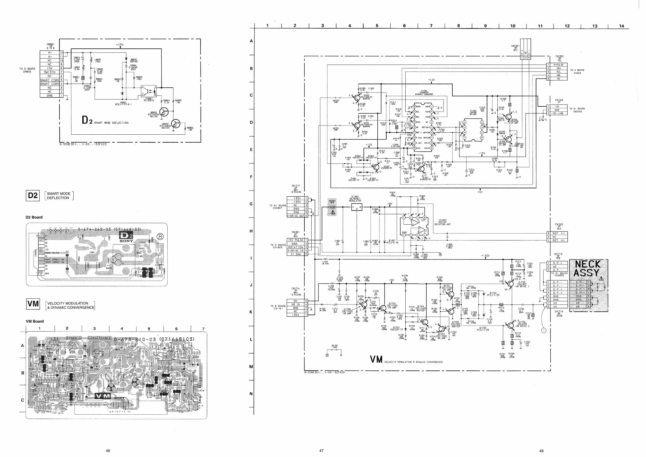
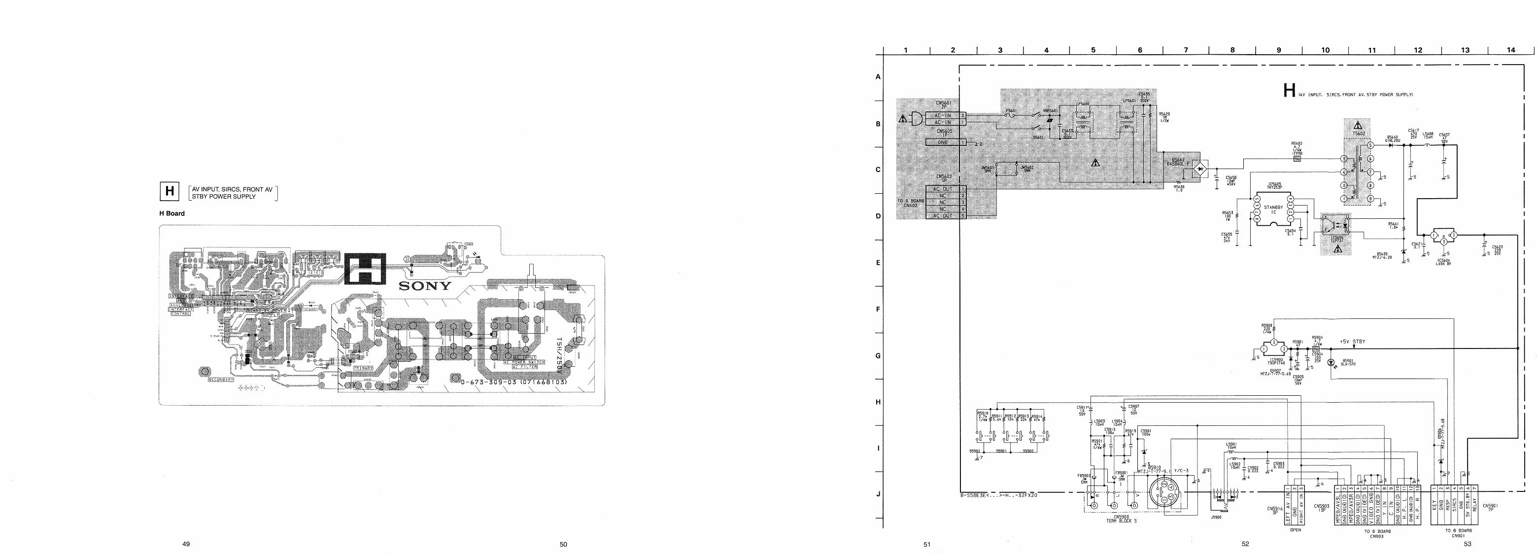
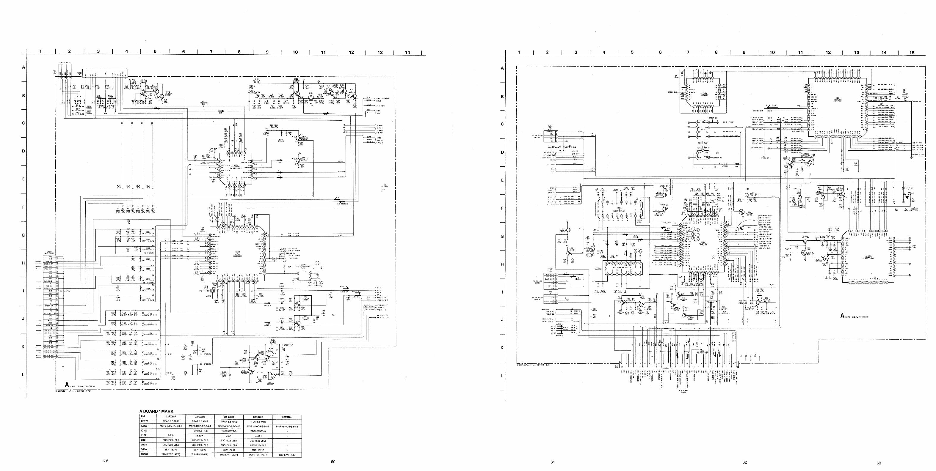
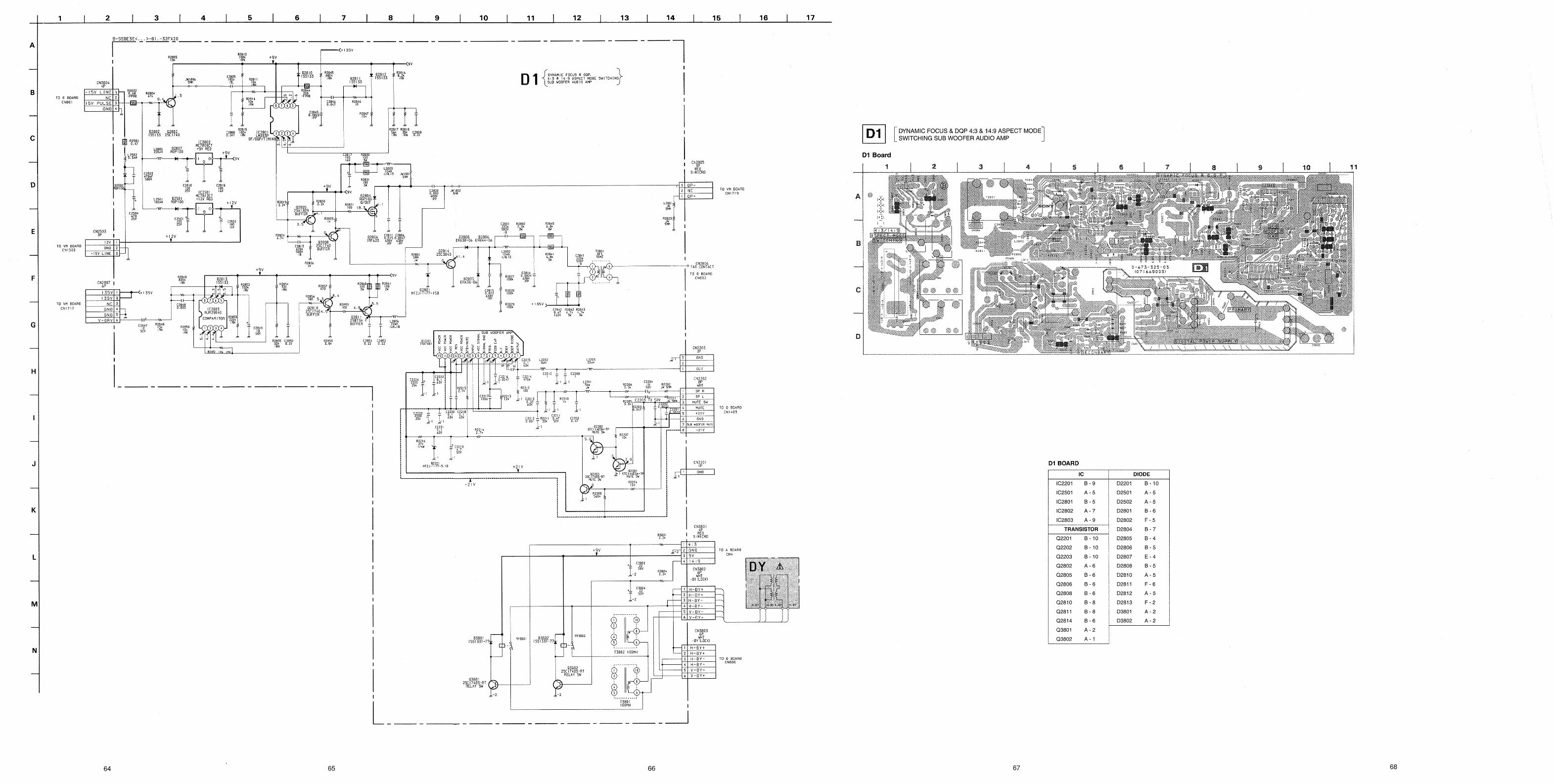
Printed Wiring Boards .....................36* C Board .....................37* D Board .....................43* D2 Board .....................46* VM Board .....................47* H Board .....................51* A Board .....................59* D1 Board .....................64
5-4. Semiconductors .....................695-5. IC Blocks .....................71
6. EXPLODED VIEWS
6-1. Chassis .....................736-2. Picture Tube .....................74
7. ELECTRICAL PARTS LIST .....................75
APRES AVOIR DECONNECTE LE CAP DE’LANODE,COURT-CIRCUITER L’ANODE DU TUBE CATHODIQUE ETCELUI DE L’ANODE DU CAP AU CHASSIS METALLIQUEDE L’APPAREIL, OU AU COUCHE DE CARBONE PEINTESUR LE TUBE CATHODIQUE OU AU BLINDAGE DU TUBECATHODIQUE.
ATTENTION !!
AFIN D’EVITER TOUT RISQUE D’ELECTROCUTION PROVENANTD’UN CHÁSSIS SOUS TENTION, UN TRANSFORMATEURD’ISOLEMENT DOIT ETRE UTILISÈ LORS DE TOUT DÈPANNAGE.LE CHÁSSIS DE CE RÈCEPTEUR EST DIRECTMENT RACCORDÈÁ L’ALIMENTATION SECTEUR.
ATTENTION AUX COMPOSANTS RELATIFS Á LASÈCURITÈ !!
LES COMPOSANTS IDENTIFIÈS PAR UNE TRAME ET PAR UNE
MARQUE SUR LES SCHÈMAS DE PRINCIPE, LES VUES EXPLOSÈES ET LES LISTES DE PIECES SONT D’UNE IMPORTANCECRITIQUE POUR LA SÈCURITÈ DU FONCTIONNEMENT, NE LESREMPLACER QUE PAR DES COMPSANTS SONY DONT LE NUMÈRODE PIÈCE EST INDIQUÈ DANS LE PRÈSENT MANUEL OU DANSDES SUPPLÈMENTS PUBLIÈS PAR SONY.
6
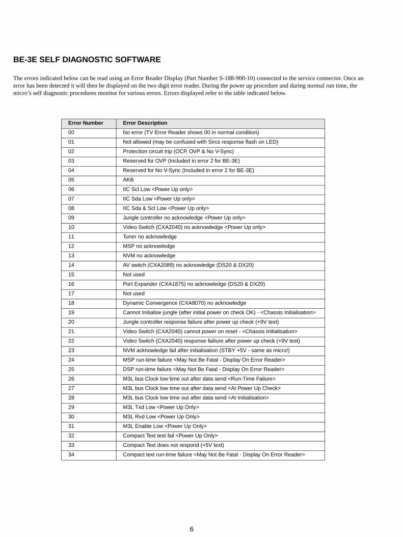
BE-3E SELF DIAGNOSTIC SOFTWARE
The errors indicated below can be read using an Error Reader Display (Part Number S-188-900-10) connected to the service connector. Once an error has been detected it will then be displayed on the two digit error reader. During the power up procedure and during normal run time, the micro’s self diagnostic procedures monitor for various errors. Errors displayed refer to the table indicated below.
Error Number Error Description
00 No error (TV Error Reader shows 00 in normal condition)
01 Not allowed (may be confused with Sircs response flash on LED)
02 Protection circuit trip (OCP, OVP & No V-Sync)
03 Reserved for OVP (Included in error 2 for BE-3E)
04 Reserved for No V-Sync (Included in error 2 for BE-3E)
05 AKB
06 IIC Scl Low <Power Up only>
07 IIC Sda Low <Power Up only>
08 IIC Sda & Scl Low <Power Up only>
09 Jungle controller no acknowledge <Power Up only>
10 Video Switch (CXA2040) no acknowledge <Power Up only>
11 Tuner no acknowledge
12 MSP no acknowledge
13 NVM no acknowledge
14 AV switch (CXA2089) no acknowledge (DS20 & DX20)
15 Not used
16 Port Expander (CXA1875) no acknowledge (DS20 & DX20)
17 Not used
18 Dynamic Convergence (CXA8070) no acknowledge
19 Cannot Initialise jungle (after initial power on check OK) - <Chassis Initialisation>
20 Jungle controller response failure after power up check (+9V test)
21 Video Switch (CXA2040) cannot power on reset - <Chassis Initialisation>
22 Video Switch (CXA2040) response failiure after power up check (+9V test)
23 NVM acknowledge fail after initialisation (STBY +5V - same as micro!)
24 MSP run-time failure <May Not Be Fatal - Display On Error Reader>
25 DSP run-time failure <May Not Be Fatal - Display On Error Reader>
26 M3L bus Clock low time out after data send <Run-Time Failure>
27 M3L bus Clock low time out after data send <At Power Up Check>
28 M3L bus Clock low time out after data send <At Initialisation>
29 M3L Txd Low <Power Up Only>
30 M3L Rxd Low <Power Up Only>
31 M3L Enable Low <Power Up Only>
32 Compact Text test fail <Power Up Only>
33 Compact Text does not respond (+5V test)
34 Compact text run-time failure <May Not Be Fatal - Display On Error Reader>

7
Protection Error (Error 2):
AKB Error (Error 5):
Startup Diagnostic Errors (Errors 6-18, 27, 29-32):
10090807050 60403020100
Time / seconds
IKRReturn
A B C D E F
A. IKR Return first goes high after 12 seconds.B. Micro begins checking IKR Return status 20 seconds after power on.C. Micro detects IKR return = 0.D. Micro detects that IKR has been 0 for 10 seconds; NVM counter is incremented and the LED
starts flashing (flashes 5 times, off for 2 seconds, flashes 5 times, etc.E. Micro detects that IKR=1; LED continues to flash.F. Micro detects that IKR has been high for 10 seconds; LED stops flashing.
NVM Error Description
6 SCL pin low
7 SDA pin low
8 Both SCL and the SDA pins are low
9 No acknowledge from the jungle (CXA2076)
10 No acknowledge from the video switch (CXA2040)
11 No acknowledge from the tuner
12 No acknowledge from the MSP
13 No acknowledge from the NVM
14 No acknowledge from the CXA2089 video switch (DS20 & DX20)
16 No acknowledge from the CXA1875 video Port Expander (DS20 & DX20)
18 No acknowledge from the Dynamic Convergence (CXA8070)
27 M3L_TXD pin low after Compact Text RAM test.
29 M3L_TXD pin low
30 M3L_RXD pin low
31 M3LEN pin low
32 Compact Text RAM test fail
Once every main loop (approximately 200ms OSD mode, 50ms text or menu mode), the micro checks the protection pin (pin 66). If the protection pin is high 6 successive times, a protection error is diagnosed. The protection pin is not checked during the first 3 - 4 seconds after AC on.If this error is diagnosed, the respective NVM register will be updated and the set goes straight into diagnostic standby with 2 flashes - no reset is attempted.
Once every main loop the micro checks the AKB stability by reading the IKR return from the Jungle IC. IKR=1 means that the AKB is stable, IKR=0 means that the AKB is unstable. If the AKB status is unstable for 10 seconds, an AKB error is diagnosed. AKB stability is not checked during the first 20 seconds after AC switch on.If this error is diagnosed, the respective NVM register will be updated and the response LED will flash 5 times continually, but the set will not go into standby mode. If the AKB status becomes stable, and remains stable for 10 seconds, the LED will stop flashing.
If any of these errors are detected, the respective NVM register will be incremented. The software will then carry on with the power up sequence.
8
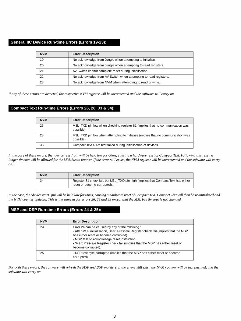
General IIC Device Run-time Errors (Errors 19-23):
Compact Text Run-time Errors (Errors 26, 28, 33 & 34):
MSP and DSP Run-time Errors (Errors 24 & 25):
If any of these errors are detected, the respective NVM register will be incremented and the software will carry on.
NVM Error Description
19 No acknowledge from Jungle when attempting to initialise.
20 No acknowledge from Jungle when attempting to read registers.
21 AV Switch cannot complete reset during initialisation.
22 No acknowledge from AV Switch when attempting to read registers.
23 No acknowledge from NVM when attempting to read or write.
In the case of these errors, the ‘device reset’ pin will be held low for 60ms, causing a hardware reset of Compact Text. Following this reset, a longer timeout will be allowed for the M3L bus to recover. If the error still exists, the NVM register will be incremented and the software will carry on.
NVM Error Description
26 M3L_TXD pin low when checking register 81 (implies that no communication was possible).
28 M3L_TXD pin low when attempting to initialise (implies that no communication was possible).
33 Compact Text RAM test failed during initialisation of devices.
In the case, the ‘device reset’ pin will be held low for 60ms, causing a hardware reset of Compact Text. Compact Text will then be re-initialised and the NVM counter updated. This is the same as for errors 26, 28 and 33 except that the M3L bus timeout is not changed.
NVM Error Description
34 Register 81 check fail, but M3L_TXD pin high (implies that Compact Text has either reset or become corrupted).
For both these errors, the software will refresh the MSP and DSP registers. If the errors still exist, the NVM counter will be incremented, and the software will carry on.
NVM Error Description
24 Error 24 can be caused by any of the following :- After MSP initialisation, Scart Prescale Register check fail (implies that the MSP has either reset or become corrupted).- MSP fails to acknowledge reset instruction.- Scart Prescale Register check fail (implies that the MSP has either reset or become corrupted).
25 - DSP test byte corrupted (implies that the MSP has either reset or become corrupted).
9
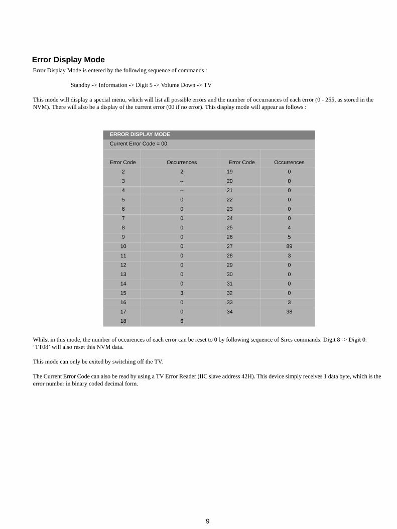
Error Display ModeError Display Mode is entered by the following sequence of commands :
Standby -> Information -> Digit 5 -> Volume Down -> TV
This mode will display a special menu, which will list all possible errors and the number of occurrances of each error (0 - 255, as stored in the NVM). There will also be a display of the current error (00 if no error). This display mode will appear as follows :
ERROR DISPLAY MODE
Current Error Code = 00
Error Code Occurrences Error Code Occurrences
2 2 19 0
3 -- 20 0
4 -- 21 0
5 0 22 0
6 0 23 0
7 0 24 0
8 0 25 4
9 0 26 5
10 0 27 89
11 0 28 3
12 0 29 0
13 0 30 0
14 0 31 0
15 3 32 0
16 0 33 3
17 0 34 38
18 6
Whilst in this mode, the number of occurences of each error can be reset to 0 by following sequence of Sircs commands: Digit 8 -> Digit 0.‘TT08’ will also reset this NVM data.
This mode can only be exited by switching off the TV.
The Current Error Code can also be read by using a TV Error Reader (IIC slave address 42H). This device simply receives 1 data byte, which is the error number in binary coded decimal form.
10
8
Overview
Overview of the remote control buttons
To mute sound
Press to mute TV sound. Pressagain to restore the sound.
To display sound menu
Press to change the sound settings.Press again to remove the display.
To adjust TV volume
Press to adjust the volume of the TV.
To temporarily switch off TV
Press to temporarily switch off TV. Press againto switch on TV from standby mode.To save energy we recommend switching offcompletely when TV is not in use.NOTE: After 15 -30 minutes without a TVsignal and without any button being pressed, theTV switches automatically into standby mode.
To reveal on screen information
Press to reveal all on-screen indications.Press again to cancel.
To select channels
Press to select channels.
To change screen format
Press to change the size of the screen.To display picture menu
Press to change the picture settings.Press again to remove the display.
To select teletext
Press to switch on Teletext.
To return to TV mode
Press to return to the normal operationfrom teletext mode or standby mode.
To select menu items
Use the OK button and arrow keys toselect the options available in the menusystem of this TV.
To select input signal or freeze teletext
Press to select inputs from the TV sockets (seeUsing Optional Equipment section). In teletextmode, press to freeze the displayed page. Pressonce again to cancel.
To display the menuPress if you wish to use the TV menusystem. Press again to remove the menufrom the TV screen.
To select channelsPress the numbered buttons to select channels.
For double digit programme numbers, e.g.23,press -/-- first, then the buttons 2 and 3.If you enter an incorrect first digit, this shouldbe corrected by entering another digit (0 - 9)and then selecting -/-- button again to enter theprogramme number of your choice.
This button has no function
To return to previous channelPress to return to the previous channelyou were watching. Note: This can bedone only after watching the presentchannel for 5 seconds
6
6. Automatically tuning the TV
1 When switching on the TV for the first time, the‘LANGUAGE’ menu appears automatically on the TVscreen enabling you to select in which language youwish to read the TV menu screens. Press the UP andDOWN arrow keys on the remote control to select yourlanguage then press the OK button to confirm yourselection.
2 The ‘AUTO TUNE’ menu appears on the TV screen inyour selected language. Press the UP and DOWN arrowkeys to select ‘YES’ then press the OK button toconfirm.
3 A new menu appears asking you to check that theantenna is connected. Ensure that the antenna isconnected then press the OK button to confirm. The TVnow starts to automatically search and store all availablechannels for you. Please be patient and do not press anybuttons.
4 When the TV has finished tuning in all availablechannels, the ‘PROGRAMME SORTING’ menu appearson the TV screen which enables you to change thechannel order on your TV. If you wish to change theorder of any of the TV channels, press the PROGR+/-button on your remote control until the channel you wishto rearrange appears on the screen. Press the UP orDOWN arrow keys to select the new programme numberposition for your selected channel. Press the OK buttonto confirm. Repeat this procedure if you wish to changethe order of other channels on your TV.
5 Press the MENU button to remove the menu from theTV screen.
6 Press the PROGR+/- or the numbered buttons on theremote control to view the TV channels.
Quick Start Guide
When you first switch on the TV, the following sequence of menu screens appear on the TV enabling you to 1) choose alanguage for the TV menu screens, 2) add channels to the TV, 3) arrange the channels.
6 B/GSYSPROG
C26CHAN
- - - - - LABEL
AUTO PROGRAMME
AUTO PROGRAMME
Please confirm thatantenna is connected
Confirm: OK
EnglishDeutschFrançaisItalianoNederlandsPolskiÈČeskyMagyarEλλnν kά
LANGUAGE
YesNo
Do you want to start automatic tuning?
Confirm: OK
0123456789
B/GB/GB/GB/GB/GB/GB/GB/GB/GB/G
SYSPROGC28C29C35C38C40C42C55C56C57C58
CHANBBC-WVHS-2CNN- - - - - - - MV-CHVHS-1 - - - - - 8MM - - - - - - - - - -
LABEL
PROGRAMME SORTING
Select: OK Exit: MENU
0123456789
B/GB/GB/GB/GB/GB/GB/GB/GB/GB/G
SYSPROGC28C29C35C38C40C42C55C56C57C58
CHANBBC-WVHS-2CNN- - - - - - - MV-CHVHS-1 - - - - - 8MM - - - - - - - - - -
LABEL
PROGRAMME SORTING
Select Position: 4$ Confirm: OK
SECTION 1 GENERALThe operating instructions mentioned here are partial abstractsfrom the Operating Manual. The page numbers of the Operating Instruction Manual remain as in the manual.
11
9
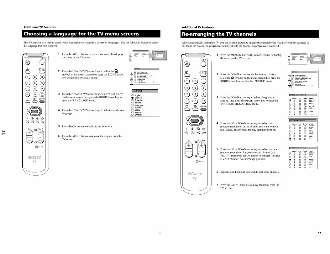
Choosing a language for the TV menu screens
1 Press the MENU button on the remote control to displaythe menu on the TV screen.
2 Press the UP or DOWN arrow keys to select the symbol on the menu screen then press the RIGHT arrowkey to enter the ‘PRESET’ menu
3 Press the UP or DOWN arrow keys to select ‘Language’on the menu screen then press the RIGHT arrow key toenter the ‘LANGUAGE’ menu.
4 Press the UP or DOWN arrow keys to select your chosenlanguage.
5 Press the OK button to confirm your selection.
6 Press the MENU button to remove the display from theTV screen.
Additional TV Features
The TV consists of a menu system which can appear on screen in a variety of languages. Use the following feature to selectthe language that best suits you.
EnglishDeutschFrançaisItalianoNederlandsPolskiÈČeskyMagyarEλλnν kά
LANGUAGE
PICTURE CONTROL
ContrastResetFormatFormat
Picture Mode Personal . . . . . . . . .
Wide
PICTURE CONTROL
ContrastResetFormatFormat
Picture Mode Personal . . . . . . . . .
Wide
Auto ProgrammeManual ProgrammeFurther Programme PresetAV Label PresetProgramme SortingParental LockLanguagePicture Rotation 0
PRESET
11
Re-arranging the TV channels
Additional TV Features
After automatically tuning the TV, you can use this feature to change the channel order. You may wish for example toexchange the channel on programme number 8 with the channel on programme number 4.
1 Press the MENU button on the remote control to displaythe menu on the TV screen.
2 Press the DOWN arrow key on the remote control toselect the symbol on the menu screen then press theRIGHT arrow key to enter the ‘PRESET’ menu.
3 Press the DOWN arrow key to select ‘ProgrammeSorting’ then press the RIGHT arrow key to enter the‘PROGRAMME SORTING’ menu.
4 Press the UP or DOWN arrow keys to select theprogramme position of the channel you want to move(e.g. PROG 8) then press the OK button to confirm.
5 Press the UP or DOWN arrow keys to select the newprogramme position for your selected channel (e.g.PROG 4) then press the OK button to confirm. The twoselected channels now exchange position.
6 Repeat steps 4 and 5 if you wish to sort other channels.
7 Press the MENU button to remove the menu from theTV screen.
PICTURE CONTROL
ContrastResetFormatFormat
Picture Mode Personal . . . . . . . . .
Wide
PICTURE CONTROL
ContrastResetFormatFormat
Picture Mode Personal . . . . . . . . .
Wide
Auto ProgrammeManual ProgrammeFurther Programme PresetAV Label PresetProgramme SortingParental LockLanguagePicture Rotation 0
PRESET
0123456789
BGBGBGBGBGBGBGBGBGBG
SYSPROGC28C29C35C38C40C42C55C56C57C58
CHANBBC-WVHS-2CNN- - - - - - - MV-CHVHS-1 - - - - - 8MM - - - - - - - - - -
LABEL
PROGRAMME SORTING
0123456789
BGBGBGBGBGBGBGBGBGBG
SYSPROGC28C29C35C38C40C42C55C56C57C58
CHANBBC-WVHS-2CNN- - - - - - - MV-CHVHS-1 - - - - - 8MM - - - - - - - - - -
LABEL
PROGRAMME SORTING
0123456789
BGBGBGBGBGBGBGBGBGBG
SYSPROGC28C29C35C38C40C42C55C56C57C58
CHANBBC-WVHS-2CNN- - - - - - - MV-CHVHS-1 - - - - - 8MM - - - - - - - - - -
LABEL
PROGRAMME SORTING
12
12
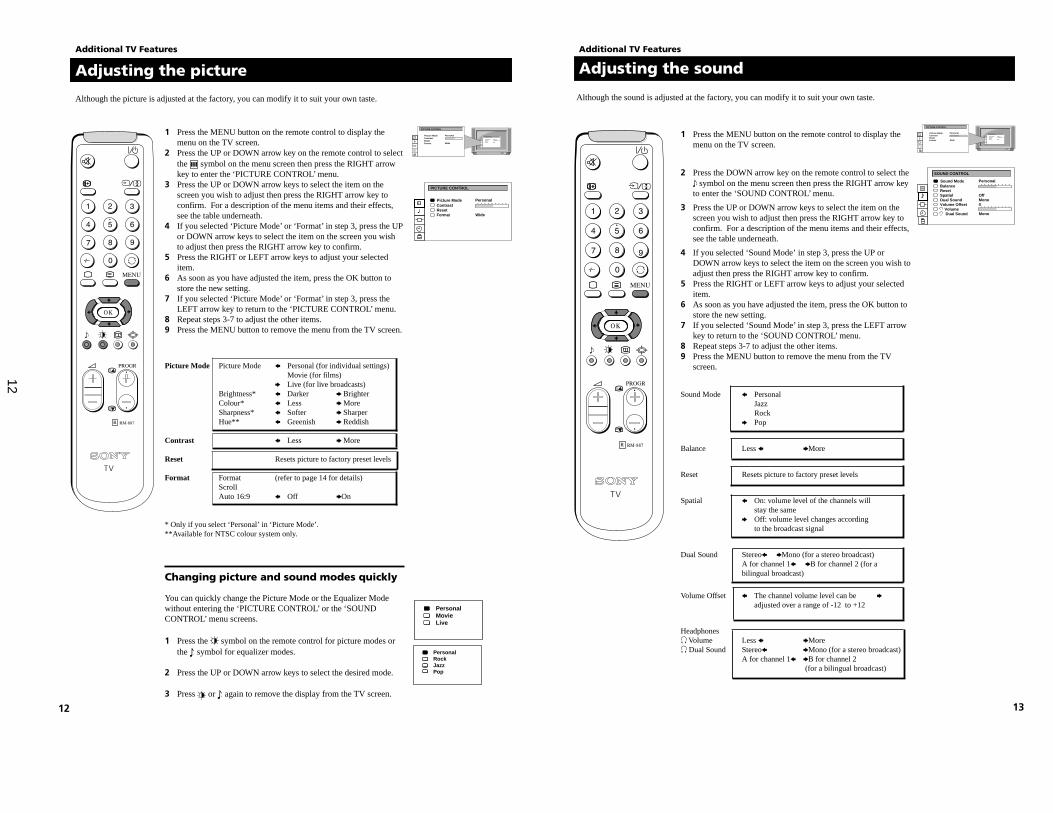
Adjusting the picture
Additional TV Features
Although the picture is adjusted at the factory, you can modify it to suit your own taste.
1 Press the MENU button on the remote control to display themenu on the TV screen.
2 Press the UP or DOWN arrow key on the remote control to selectthe symbol on the menu screen then press the RIGHT arrowkey to enter the ‘PICTURE CONTROL’ menu.
3 Press the UP or DOWN arrow keys to select the item on thescreen you wish to adjust then press the RIGHT arrow key toconfirm. For a description of the menu items and their effects,see the table underneath.
4 If you selected ‘Picture Mode’ or ‘Format’ in step 3, press the UPor DOWN arrow keys to select the item on the screen you wishto adjust then press the RIGHT arrow key to confirm.
5 Press the RIGHT or LEFT arrow keys to adjust your selecteditem.
6 As soon as you have adjusted the item, press the OK button tostore the new setting.
7 If you selected ‘Picture Mode’ or ‘Format’ in step 3, press theLEFT arrow key to return to the ‘PICTURE CONTROL’ menu.
8 Repeat steps 3-7 to adjust the other items.9 Press the MENU button to remove the menu from the TV screen.
Picture Mode Picture Mode B Personal (for individual settings)Movie (for films)
b Live (for live broadcasts)Brightness* B Darker b BrighterColour* B Less b MoreSharpness* B Softer b SharperHue** B Greenish b Reddish
Contrast B Less b More
Reset Resets picture to factory preset levels
Format Format (refer to page 14 for details)ScrollAuto 16:9 B Off bOn
* Only if you select ‘Personal’ in ‘Picture Mode’.**Available for NTSC colour system only.
Changing picture and sound modes quickly
You can quickly change the Picture Mode or the Equalizer Modewithout entering the ‘PICTURE CONTROL’ or the ‘SOUNDCONTROL’ menu screens.
1 Press the symbol on the remote control for picture modes orthe symbol for equalizer modes.
2 Press the UP or DOWN arrow keys to select the desired mode.
3 Press or again to remove the display from the TV screen.
PICTURE CONTROL
ContrastResetFormatFormat
Picture Mode Personal . . . . . . . . .
Wide
PICTURE CONTROL
ContrastResetFormatFormat
Picture Mode Personal . . . . . . . . .
Wide
PICTURE CONTROL
ContrastResetFormatFormat
Picture Mode Personal . . . . . . . . .
Wide
Personal MovieLive
PersonalRockJazzPop
13
Additional TV Features
Adjusting the sound
1 Press the MENU button on the remote control to display themenu on the TV screen.
2 Press the DOWN arrow key on the remote control to select the symbol on the menu screen then press the RIGHT arrow key
to enter the ‘SOUND CONTROL’ menu.
3 Press the UP or DOWN arrow keys to select the item on thescreen you wish to adjust then press the RIGHT arrow key toconfirm. For a description of the menu items and their effects,see the table underneath.
4 If you selected ‘Sound Mode’ in step 3, press the UP orDOWN arrow keys to select the item on the screen you wish toadjust then press the RIGHT arrow key to confirm.
5 Press the RIGHT or LEFT arrow keys to adjust your selecteditem.
6 As soon as you have adjusted the item, press the OK button tostore the new setting.
7 If you selected ‘Sound Mode’ in step 3, press the LEFT arrowkey to return to the ‘SOUND CONTROL’ menu.
8 Repeat steps 3-7 to adjust the other items.9 Press the MENU button to remove the menu from the TV
screen.
Sound Mode B PersonalJazzRock
b Pop
Balance Less B bMore
Reset Resets picture to factory preset levels
Spatial B On: volume level of the channels willstay the same
b Off: volume level changes accordingto the broadcast signal
Dual Sound StereoB bMono (for a stereo broadcast)A for channel 1B bB for channel 2 (for abilingual broadcast)
Volume Offset B The channel volume level can be badjusted over a range of -12 to +12
Headphones2 Volume Less B bMore2 Dual Sound StereoB bMono (for a stereo broadcast)
A for channel 1B bB for channel 2 (for a bilingual broadcast)
Although the sound is adjusted at the factory, you can modify it to suit your own taste.
SOUND CONTROL
BalanceResetSpatialDual SoundVolume Offset Volume Dual Sound
Sound Mode Personal . . . . . . . . .
OffMono0
Mono
. . . . . . . . .
PICTURE CONTROL
ContrastResetFormatFormat
Picture Mode Personal . . . . . . . . .
Wide
PICTURE CONTROL
ContrastResetFormatFormat
Picture Mode Personal . . . . . . . . .
Wide
13
15
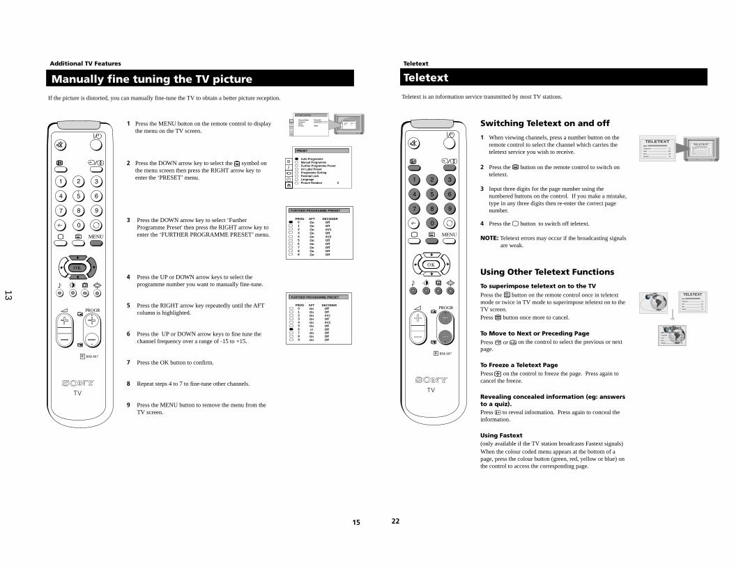
Manually fine tuning the TV picture
If the picture is distorted, you can manually fine-tune the TV to obtain a better picture reception.
1 Press the MENU button on the remote control to displaythe menu on the TV screen.
2 Press the DOWN arrow key to select the symbol onthe menu screen then press the RIGHT arrow key toenter the ‘PRESET’ menu.
3 Press the DOWN arrow key to select ‘FurtherProgramme Preset' then press the RIGHT arrow key toenter the ‘FURTHER PROGRAMME PRESET’ menu.
4 Press the UP or DOWN arrow keys to select theprogramme number you want to manually fine-tune.
5 Press the RIGHT arrow key repeatedly until the AFTcolumn is highlighted.
6 Press the UP or DOWN arrow keys to fine tune thechannel frequency over a range of -15 to +15.
7 Press the OK button to confirm.
8 Repeat steps 4 to 7 to fine-tune other channels.
9 Press the MENU button to remove the menu from theTV screen.
PICTURE CONTROL
ContrastResetFormatFormat
Picture Mode Personal . . . . . . . . .
Wide
PICTURE CONTROL
ContrastResetFormatFormat
Picture Mode Personal . . . . . . . . .
Wide
Auto ProgrammeManual ProgrammeFurther Programme PresetAV Label PresetProgramme SortingParental LockLanguagePicture Rotation 0
PRESET
0123456789
PROGOffOffAV1OffAV2OffOffOffOffOff
DECODEROnOnOnOnOnOnOnOnOnOn
AFT
FURTHER PROGRAMME PRESET
0123456789
PROGOffOffAV1OffAV2OffOffOffOffOff
DECODEROnOnOnOnOnOn10OnOnOn
AFT
FURTHER PROGRAMME PRESET
Additional TV Features
22
TeletextTeletext
Switching Teletext on and off
1 When viewing channels, press a number button on theremote control to select the channel which carries theteletext service you wish to receive.
2 Press the button on the remote control to switch onteletext.
3 Input three digits for the page number using thenumbered buttons on the control. If you make a mistake,type in any three digits then re-enter the correct pagenumber.
4 Press the button to switch off teletext.
NOTE: Teletext errors may occur if the broadcasting signals are weak.
Using Other Teletext Functions
To superimpose teletext on to the TVPress the button on the remote control once in teletextmode or twice in TV mode to superimpose teletext on to theTV screen.Press button once more to cancel.
To Move to Next or Preceding PagePress or on the control to select the previous or nextpage.
To Freeze a Teletext PagePress on the control to freeze the page. Press again tocancel the freeze.
Revealing concealed information (eg: answersto a quiz).Press to reveal information. Press again to conceal theinformation.
Using Fastext(only available if the TV station broadcasts Fastext signals)When the colour coded menu appears at the bottom of apage, press the colour button (green, red, yellow or blue) onthe control to access the corresponding page.
Index
TELETEXTTELETEXT
Programme
News
Sport
Weather
25
153
101
98
Index
TELETEXTTELETEXT
Programme
News
Sport
Weather
25
153
101
98
Index
TELETEXTTELETEXT
Programme
News
Sport
Weather
25
153
101
98
Index
TELETEXTTELETEXT
Programme
News
Sport
Weather
25
153
101
98
Teletext is an information service transmitted by most TV stations.
14
26
Additional Information
SpecificationsTV systemB/G/H
Colour systemPAL, SECAMNTSC 3.58, 4.43 (only Video In)
Channel coverageSee ‘Receivable Channels’ table on next page
Picture tubeKV-28FX20D:FD Trinitron WIDEApprox. 71 cm (28 inches) (Approx. 66 cm picture measured diagonally),102° deflectionKV-32FX20D:FD Trinitron WIDEApprox. 82 cm (32 inches) (Approx. 76 cm picture measured diagonally),102° deflection
Rear Terminals 1 21-pin Euro connector (CENELEC standard) including audio/video
input, RGB input
2/ s 2 21-pin Euro connector (CENELEC standard) including audio/videoinput, S-video input, Monitor audio/video output
Audio outputs - phono jacks
Front Terminals 3 video input - phono jack
3 audio inputs - phono jackss 2 S video input - 4 pin DIN
Headphones jack - minijack stereo
Sound output:Left, Right 2x20W (music power)Subwoofer 20W (music power)
Power consumptionKV-28FX20D: 123 WKV-32FX20D: 120 W
Dimensions (wxhxd)KV-28FX20D: Approx. 761 x 496 x 525 mmKV-32FX20D: Approx. 874 x 563 x 571 mm
Weight
KV-28FX20D: Approx. 44.0 kgKV-32FX20D: Approx. 62.0 kg
Accessories suppliedRM-887 Remote Control (1)IEC designated size AA battery (2)
Other featuresTELETEXT
Design and specifications are subject to change without notice.
28
Troubleshooting
Additional Information
Problem SolutionNo picture (screen is dark), • Plug the TV in.no sound • Press the button on the front of TV.
• If the indicator is on press / button or a
programme number button on the remote control.• Check the aerial connection.• Check that the selected video source is on.• Turn the TV off for 3 or 4 seconds and then turn it on
again using the button on the front of the TV.
Poor or no picture (screen is dark), • Using the MENU system, select the Picturebut good sound. Control and Picture Mode displays. Adjust the
contrast, brightness, and colour levels.• From the Picture Control display select RESET to
return to factory settings.
Poor picture quality when watching • Press the button repeatedly on the remote controla RGB video source. until the RGB symbol is displayed on the screen.
Good picture, no sound • Press the +/– button on the remote control.
• If is displayed on the screen, press the buttonon the remote control.
No colour on colour programmes • Using the MENU system, select the Picture Modedisplay. Adjust the the colour level setting.
• From the Picture Control display select RESET toreturn to factory settings.
Distorted picture when changing • Turn off any equipment connected to the 21 pinprogrammes or selecting teletext Euro connectors on the rear of the TV.
Remote control does not function • Replace the batteries.
The standby indicator on the TV • Contact your nearest Sony service centre.flashes
• If you continue to have these problems, have your TV serviced by qualified personnel.• NEVER open the casing yourself.
Here are some simple solutions to problems which may affect the picture and sound.
15
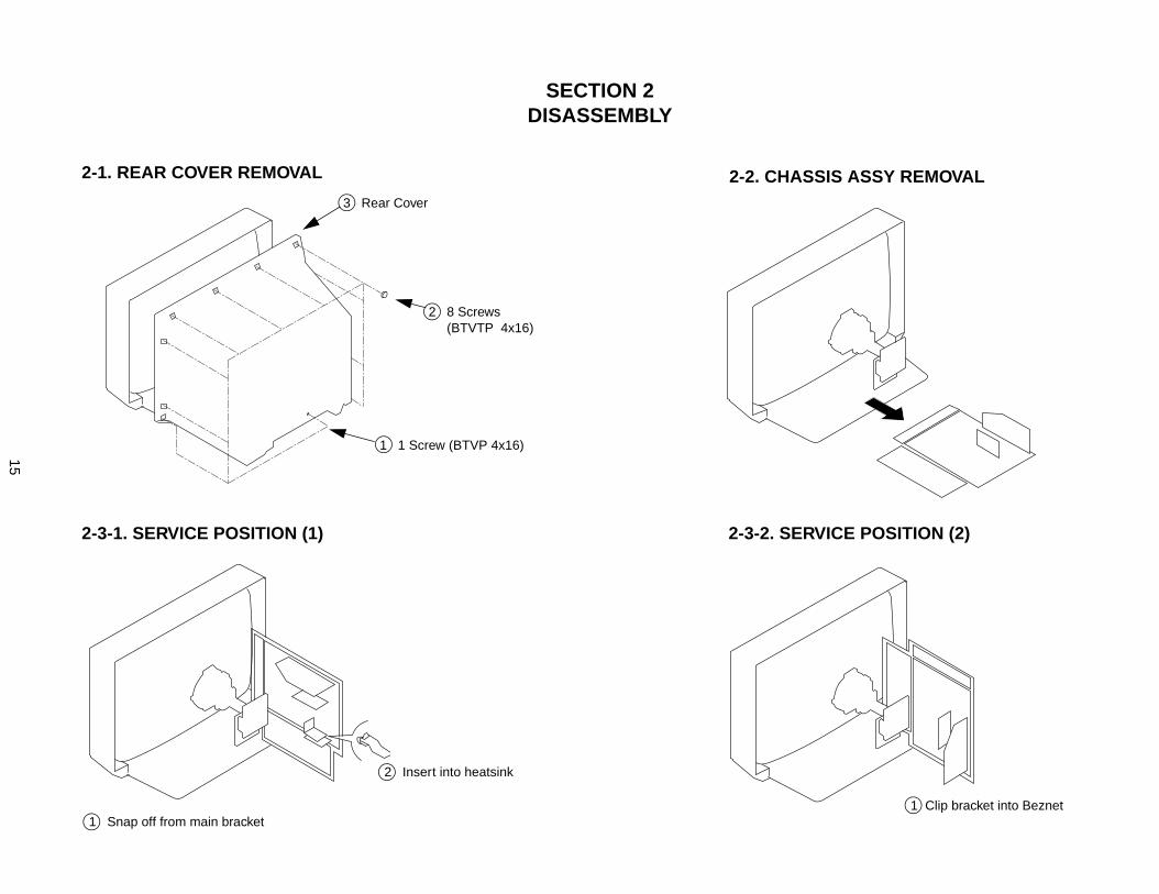
SECTION 2DISASSEMBLY
3 Rear Cover
1 1 Screw (BTVP 4x16)
2-1. REAR COVER REMOVAL 2-2. CHASSIS ASSY REMOVAL
2-3-2. SERVICE POSITION (2) 2-3-1. SERVICE POSITION (1)
2 8 Screws (BTVTP 4x16)
1 Snap off from main bracket
2 Insert into heatsink
1 Clip bracket into Beznet
16
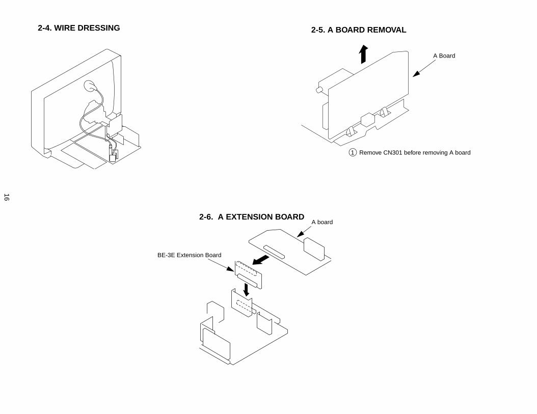
2-4. WIRE DRESSING 2-5. A BOARD REMOVAL
2-6. A EXTENSION BOARD
1 Remove CN301 before removing A board
A Board
A board
BE-3E Extension Board
17
5 Neck assy
Cushion
8 Degaussing coils
9 Spring Extension
2 Chassis assy
10 Four PT screws
11 Picture tube
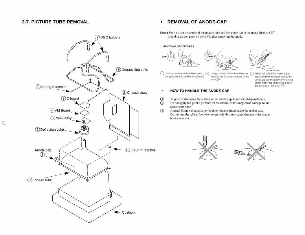
2-7. PICTURE TUBE REMOVAL
Anode button
a
* REMOVING PROCEDURES.
Turn up one side of the rubber cap inthe direction indicated by the arrow a
1 2 Using a thumb pull up the rubber cap firmly in the direction indicated by the arrow b
3 When one side of the rubber cap is separated from the anode button, the anode-cap can be removed by turning up the rubber cap and pulling it up in the direction of the arrow c
b
b
c
Note : Short circuit the anode of the picture tube and the anode cap to the metal chassis, CRT shield or carbon paint on the CRT, after removing the anode.
• REMOVAL OF ANODE-CAP
• HOW TO HANDLE THE ANODE-CAP
1 To prevent damaging the surface of the anode-cap do not use sharp materials.2 Do not apply too great a pressure on the rubber, as this may cause damage to the
anode connector.3 A metal fitting called a shatter hook terminal is fitted inside the rubber cap.
Do not turn the rubber foot over excessively this may cause damage if the shatter hook sticks out.
3 C board
Anode cap 1
7 DGC holders
6 Deflection yoke
4 VM Board
18
Fig 2NUMERICAL MARKINGS
AT
TE
NT
ION
AT
TE
NT
ION
TH
IS P
LAT
E M
US
T B
E R
EM
OV
ED
(TU
RN
180
' NO
T F
LIP
OV
ER
)A
FT
ER
CU
TT
ING
AW
AYF
OR
SA
FE
TY
RE
AS
ON
S
TH
IS P
LAT
E M
US
T B
E R
EM
OV
ED
AF
TE
R C
UT
TIN
G A
WAY
FO
R T
HE
SA
FE
TY
RE
AS
ON
.
22
22
11
44
3
44
REFITTING REFITTING
AT
TE
NT
ION
AT
TE
NT
ION
TH
IS P
LAT
E M
US
T B
E R
EM
OV
ED
(TU
RN
180
' NO
T F
LIP
OV
ER
)A
FT
ER
CU
TT
ING
AW
AYF
OR
SA
FE
TY
RE
AS
ON
S
22
22
11
Cut points
Fig 1
MAIN BRACKET
INSERT FROMTHE BOTTOMSIDE
FIG 3 Fig 4
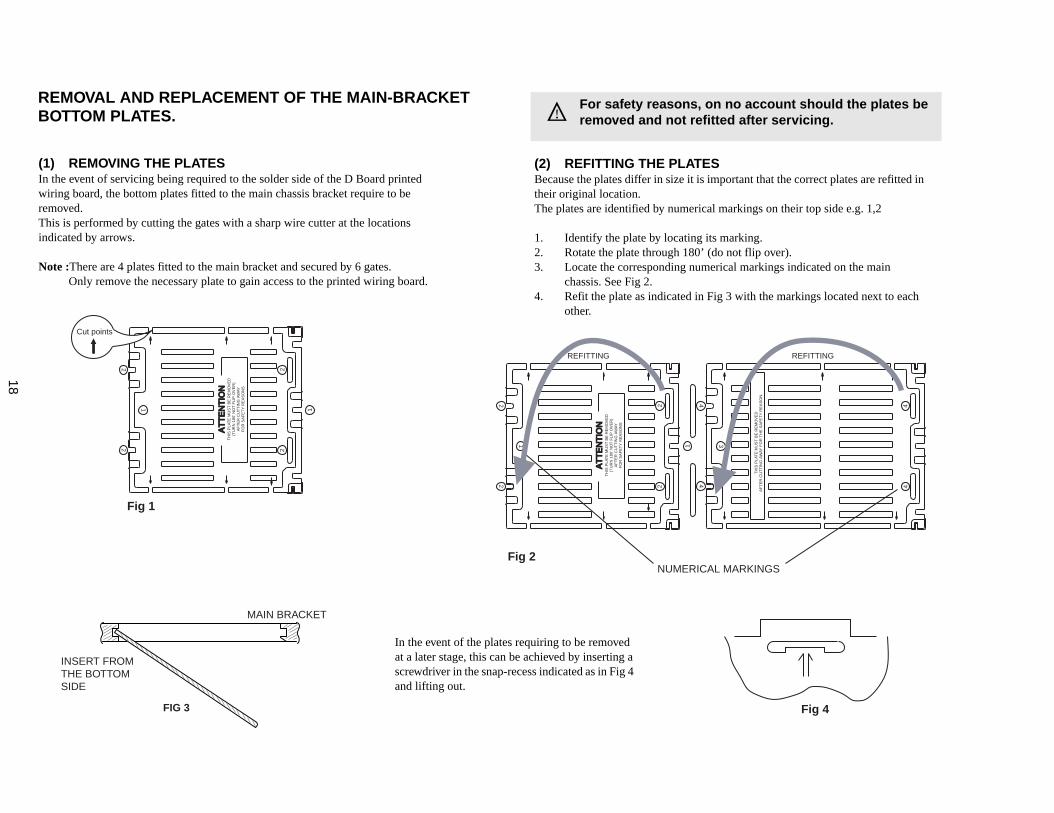
REMOVAL AND REPLACEMENT OF THE MAIN-BRACKETBOTTOM PLATES.
(1) REMOVING THE PLATESIn the event of servicing being required to the solder side of the D Board printedwiring board, the bottom plates fitted to the main chassis bracket require to beremoved.This is performed by cutting the gates with a sharp wire cutter at the locationsindicated by arrows.
Note :There are 4 plates fitted to the main bracket and secured by 6 gates.Only remove the necessary plate to gain access to the printed wiring board.
(2) REFITTING THE PLATESBecause the plates differ in size it is important that the correct plates are refitted intheir original location.The plates are identified by numerical markings on their top side e.g. 1,2
1. Identify the plate by locating its marking.2. Rotate the plate through 180’ (do not flip over).3. Locate the corresponding numerical markings indicated on the main
chassis. See Fig 2.4. Refit the plate as indicated in Fig 3 with the markings located next to each
other.
£ For safety reasons, on no account should the plates beremoved and not refitted after servicing.
In the event of the plates requiring to be removed at a later stage, this can be achieved by inserting a screwdriver in the snap-recess indicated as in Fig 4 and lifting out.
19
• When complete readjustment is necessary or a new picture tube is installed, carry out the following adjustments.
• Unless there are specific instructions to the contrary,carry out these adjustments with the rated power supply.
• Unless there are specific instructions to the contrary, set the controls and switches to the following settings:
Contrast ............... normal
Brightness ............... normal
Carry out the following adjustments in this order:3-1. Beam Landing3-2. Convergence3-3. Focus3-4. White balance
Note: Test equipment required1. Color bar/pattern generator.2. Degausser.3. Digital multimeter.4. Oscilloscope.
SECTION 3SET-UP ADJUSTMENTS
Fig.3-1
Fig.3-2
Purity
Align Pipson eachmagnet Neck assy
Align the bottom edge of the neck assy withthe G3 hole centre.
Deflection yoke
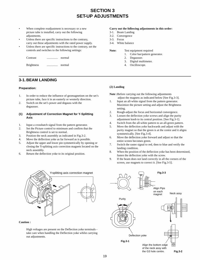
3-1. BEAM LANDING
Preparation:
1. In order to reduce the influence of geomagnetism on the set’s picture tube, face it in an easterly or westerly direction.
2. Switch on the set’s power and degauss with thedegausser.
(1) Adjustment of Correction Magnet for Y-SplittingAxis
1. Input a crosshatch signal from the pattern generator.2. Set the Picture control to minimum and confirm that the
Brightness control is set to normal.3. Position the neck assembly as indicated in Fig.3-2.4. Move the deflection yoke as far forward as is possible.5. Adjust the upper and lower pin symmetrically by opening or
closing the Y-splitting axis correction magnets located on the neck assembly.
6. Return the deflection yoke to its original position.
Caution :
High voltages are present on the Deflection yoke terminals - take care when handling the Deflection yoke whilst carrying out adjustments.
(2) Landing
Note :Before carrying out the following adjustments adjust the magnets as indicated below [See Fig.3-3].
1. Input an all-white signal from the pattern generator.Maximize the picture setting and adjust the Brightness setting.
2. Rough-adjust the focus and horizontal convergence.3. Loosen the deflection yoke screws and align the purity
adjustment knob to its central position. [See Fig.3-1].4. Switch from the all-white pattern to an all-green pattern.5. Move the deflection yoke backwards and adjust with the
purity magnet so that the green is at the centre and it aligns symmetrically. [See Fig.3-4].
6. Move the deflection yoke forward and adjust so that the entire screen becomes green.
7. Switch the raster signal to red, then to blue and verify the landing condition.
8. When the position of the deflection yoke has been determined, fasten the deflection yoke with the screw.
9. If the beam does not land correctly in all the corners of the screen, use magnets to correct it. [See Fig.3-5].
Y-splitting axis correction magnet Fig.3-3
20
Fig.3-4
Fig. 3-5
3-2. CONVERGENCE
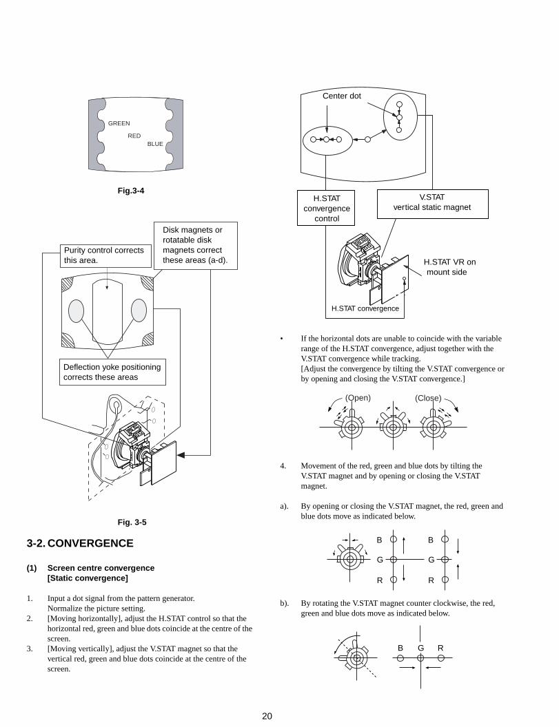
(1) Screen centre convergence [Static convergence]
1. Input a dot signal from the pattern generator. Normalize the picture setting.
2. [Moving horizontally], adjust the H.STAT control so that the horizontal red, green and blue dots coincide at the centre of the screen.
3. [Moving vertically], adjust the V.STAT magnet so that thevertical red, green and blue dots coincide at the centre of the screen.
• If the horizontal dots are unable to coincide with the variable range of the H.STAT convergence, adjust together with the V.STAT convergence while tracking.[Adjust the convergence by tilting the V.STAT convergence or by opening and closing the V.STAT convergence.]
4. Movement of the red, green and blue dots by tilting theV.STAT magnet and by opening or closing the V.STATmagnet.
a). By opening or closing the V.STAT magnet, the red, green and blue dots move as indicated below.
b). By rotating the V.STAT magnet counter clockwise, the red, green and blue dots move as indicated below.
Purity control correctsthis area.
Disk magnets orrotatable diskmagnets correctthese areas (a-d).
Deflection yoke positioningcorrects these areas
H.STATconvergence
control
V.STATvertical static magnet
Center dot
H.STAT VR onmount side
H.STAT convergence
(Open) (Close)
B
G
R
B
G
R
B G R
GREEN
BLUERED
21
B G R
B
G
R B
G
R
HMC correct ion(A) HMC correct ion(B)
A < B
A = B
R G B
R G B
A > B
A = B
R G B
R G B
C < D C = D C > D C = DRG
B
C
DC
D
R
G
B
R
GB
R
G
B
VMC correct ion(A) VMC correct ion(B)
c). By rotating the V.STAT magnet clockwise, the red, green and blue dots move in the direction indicated below.
d). By opening or closing the V.STAT magnet, the red, green and blue dots move in the direction indicated below.
Note : If the blue dot does not coincide with the red andgreen points correct the points by using the BMC[Hexapole] magnet.
5. Correction for HMC [horizontal mis-convergence] andVMC [vertical mis-convergence] by using the BMC[Hexapole] magnet.
a). HMC correction by BMC [Hexapole] magnet and movement of the electron beam.
b). VMC correction by BMC [Hexapole] magnet and movement of the electron beam.
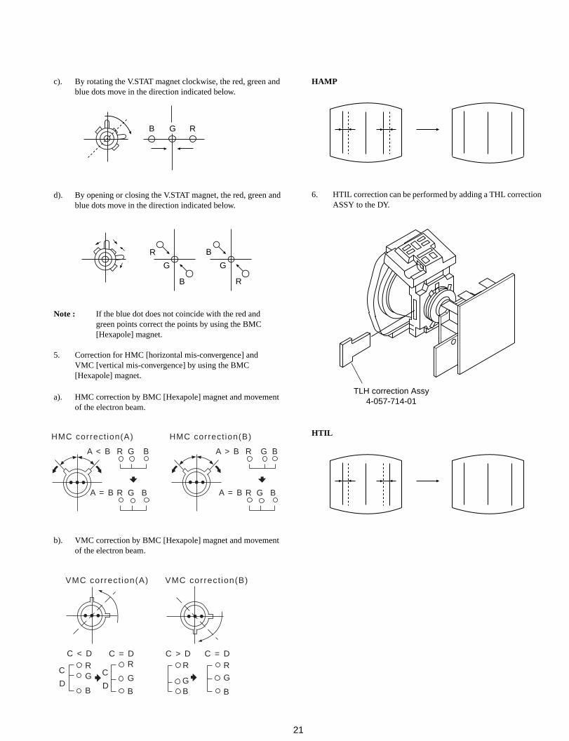
HAMP
6. HTIL correction can be performed by adding a THL correction ASSY to the DY.
HTIL
TLH correction Assy4-057-714-01
22
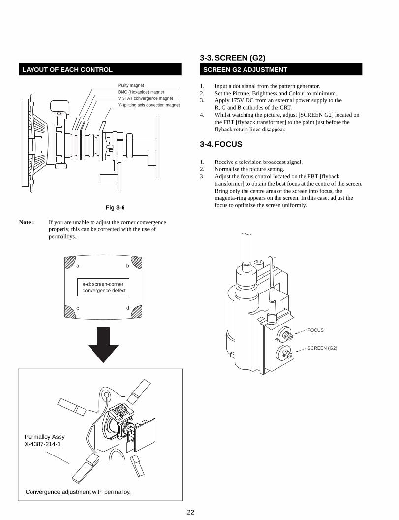
Fig 3-6
Note : If you are unable to adjust the corner convergenceproperly, this can be corrected with the use of permalloys.
3-3. SCREEN (G2)
1. Input a dot signal from the pattern generator.2. Set the Picture, Brightness and Colour to minimum.3. Apply 175V DC from an external power supply to the
R, G and B cathodes of the CRT.4. Whilst watching the picture, adjust [SCREEN G2] located on
the FBT [flyback transformer] to the point just before the flyback return lines disappear.
3-4. FOCUS
1. Receive a television broadcast signal.2. Normalise the picture setting.3 Adjust the focus control located on the FBT [flyback
transformer] to obtain the best focus at the centre of the screen.Bring only the centre area of the screen into focus, the magenta-ring appears on the screen. In this case, adjust the focus to optimize the screen uniformly.
LAYOUT OF EACH CONTROL SCREEN G2 ADJUSTMENT
Y-splitting axis correction magnet
V STAT convergence magnet
BMC (Hexaploe) magnet
Purity magnet
a-d: screen-cornerconvergence defect
a b
c d
Permalloy AssyX-4387-214-1
Convergence adjustment with permalloy.
FOCUS
SCREEN (G2)
23
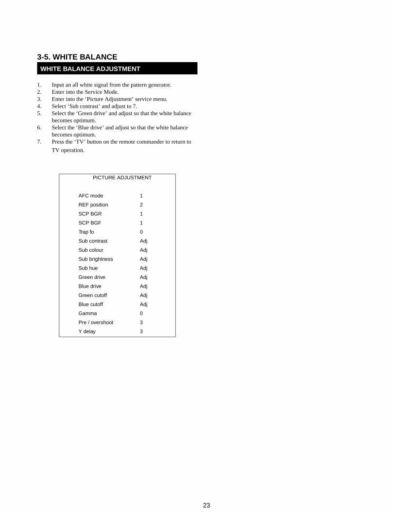
3-5. WHITE BALANCE
1. Input an all white signal from the pattern generator.2. Enter into the Service Mode.3. Enter into the ‘Picture Adjustment’ service menu.4. Select ‘Sub contrast’ and adjust to 7.5. Select the ‘Green drive’ and adjust so that the white balance
becomes optimum.6. Select the ‘Blue drive’ and adjust so that the white balance
becomes optimum.7. Press the ‘TV’ button on the remote commander to return to
TV operation.
WHITE BALANCE ADJUSTMENT
PICTURE ADJUSTMENT
AFC mode 1
REF position 2
SCP BGR 1
SCP BGF 1
Trap fo 0
Sub contrast Adj
Sub colour Adj
Sub brightness Adj
Sub hue Adj
Green drive Adj
Blue drive Adj
Green cutoff Adj
Blue cutoff Adj
Gamma 0
Pre / overshoot 3
Y delay 3
24
SECTION 4CIRCUIT ADJUSTMENTS
5+
+(ON SCREEN DISPLAY)
(DIGIT 5) (VOLUME +) (TV)
4-1. ELECTRICAL ADJUSTMENTS
Service adjustments to this model can be performedusing the supplied Remote Commander RM-887.
1. Turn on the main power switch and enter into the stand-by mode.
2. Press the following sequence of buttons on the Remote Commander.
• ‘TT--’ will appear in the upper right corner of thescreen.Other status information will also be displayed.
3. Press ‘MENU’ on the remote commander to obtain the following menu on the screen.
4. Move to the corresponding adjustment using the button on the remote commander.
5. Press the + button to enter the selected adjustment.6. Turn off the power to quit the service mode when adjustments
have been completed.
HOW TO ENTER INTO SERVICE MODE
TEST MENU
> Picture Adjustment
Geometry
Wide
IC status
MSP
Dynamic Convergence
Current TV status
PICTURE ADJUSTMENT
AFC mode 1
REF position 3
SCP BGR 1
SCP BGF 1
Trap fo 9
Sub contrast Adj
Sub colour Adj
Sub brightness Adj
Green drive Adj
Blue drive Adj
Green cutoff Adj
Blue cutoff Adj
Gamma 0
Pre / overshoot 0
Y delay 3
D Pic ON/OFF
D Colour ON/OFF
DC Transfer ON/OFF
GEOMETRY ADJUSTMENT - 4:3
V size Adj
V position Adj
S Correction Adj
V Linearity Adj
H size Adj
H position Adj
Pin Amp Adj
Pin Phase Adj
AFC Bow Adj
AFC Angle Adj
EHT V 1
EHT H 0
Lo Corn Pin Adj
Up Corn Pin Adj
WIDE ADJUSTMENT - 4:3
V Aspect 0
V Scroll 25
Upper V Lin 0
Lower V Lin 0
Left Blanking 1
Right Blanking 11
25
Same Level
B-Out Waveform
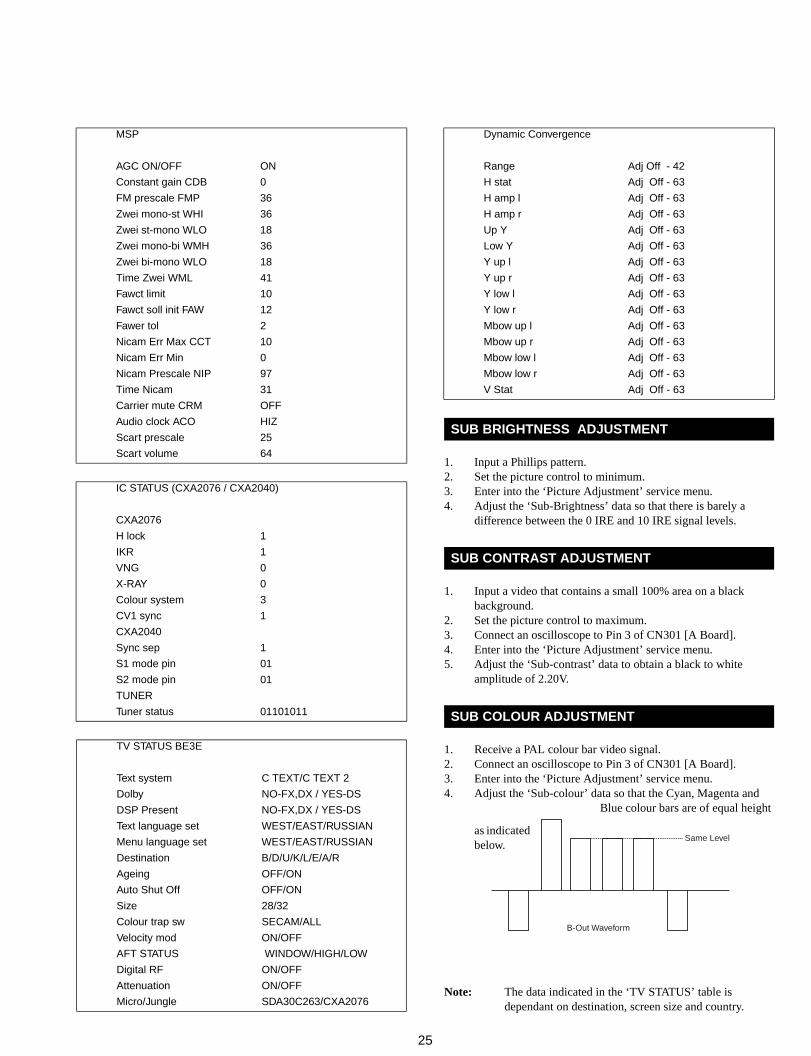
1. Input a Phillips pattern.2. Set the picture control to minimum.3. Enter into the ‘Picture Adjustment’ service menu.4. Adjust the ‘Sub-Brightness’ data so that there is barely a
difference between the 0 IRE and 10 IRE signal levels.
1. Input a video that contains a small 100% area on a black background.
2. Set the picture control to maximum.3. Connect an oscilloscope to Pin 3 of CN301 [A Board].4. Enter into the ‘Picture Adjustment’ service menu.5. Adjust the ‘Sub-contrast’ data to obtain a black to white
amplitude of 2.20V.
1. Receive a PAL colour bar video signal.2. Connect an oscilloscope to Pin 3 of CN301 [A Board].3. Enter into the ‘Picture Adjustment’ service menu.4. Adjust the ‘Sub-colour’ data so that the Cyan, Magenta and
Blue colour bars are of equal height
as indicated below.
Note: The data indicated in the ‘TV STATUS’ table isdependant on destination, screen size and country.
MSP
AGC ON/OFF ON
Constant gain CDB 0
FM prescale FMP 36
Zwei mono-st WHI 36
Zwei st-mono WLO 18
Zwei mono-bi WMH 36
Zwei bi-mono WLO 18
Time Zwei WML 41
Fawct limit 10
Fawct soll init FAW 12
Fawer tol 2
Nicam Err Max CCT 10
Nicam Err Min 0
Nicam Prescale NIP 97
Time Nicam 31
Carrier mute CRM OFF
Audio clock ACO HIZ
Scart prescale 25
Scart volume 64
IC STATUS (CXA2076 / CXA2040)
CXA2076
H lock 1
IKR 1
VNG 0
X-RAY 0
Colour system 3
CV1 sync 1
CXA2040
Sync sep 1
S1 mode pin 01
S2 mode pin 01
TUNER
Tuner status 01101011
TV STATUS BE3E
Text system C TEXT/C TEXT 2
Dolby NO-FX,DX / YES-DS
DSP Present NO-FX,DX / YES-DS
Text language set WEST/EAST/RUSSIAN
Menu language set WEST/EAST/RUSSIAN
Destination B/D/U/K/L/E/A/R
Ageing OFF/ON
Auto Shut Off OFF/ON
Size 28/32
Colour trap sw SECAM/ALL
Velocity mod ON/OFF
AFT STATUS WINDOW/HIGH/LOW
Digital RF ON/OFF
Attenuation ON/OFF
Micro/Jungle SDA30C263/CXA2076
Dynamic Convergence
Range Adj Off - 42
H stat Adj Off - 63
H amp l Adj Off - 63
H amp r Adj Off - 63
Up Y Adj Off - 63
Low Y Adj Off - 63
Y up l Adj Off - 63
Y up r Adj Off - 63
Y low l Adj Off - 63
Y low r Adj Off - 63
Mbow up l Adj Off - 63
Mbow up r Adj Off - 63
Mbow low l Adj Off - 63
Mbow low r Adj Off - 63
V Stat Adj Off - 63
SUB BRIGHTNESS ADJUSTMENT
SUB CONTRAST ADJUSTMENT
SUB COLOUR ADJUSTMENT
26
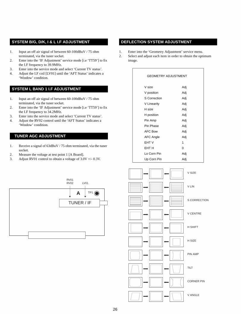
A
TUNER / IF
RV01RV02 LV01
TP1
V SIZE
V LIN
S CORRECTION
V CENTRE
H SHIFT
H SIZE
PIN AMP
TILT
CORNER PIN
V ANGLE
1. Input an off air signal of between 60-100dBuV / 75 ohm terminated, via the tuner socket.
2. Enter into the ‘IF Adjustment’ service mode [i.e ‘TT59’] to fix the I.F frequency to 39.9MHz.
3. Enter into the service mode and select ‘Current TV status’.4. Adjust the I.F coil [LV01] until the ‘AFT Status’ indicates a
‘Window’ condition.
1. Input an off air signal of between 60-100dBuV / 75 ohm terminated, via the tuner socket.
2. Enter into the ‘IF Adjustment’ service mode [i.e ‘TT59’] to fix the I.F frequency to 34.2MHz.
3. Enter into the service mode and select ‘Current TV status’.4. Adjust the RV02 control until the ‘AFT Status’ indicates a
‘Window’ condition.
1. Receive a signal of 63dBuV / 75 ohm terminated, via the tuner socket.
2. Measure the voltage at test point 1 [A Board].3. Adjust RV01 control to obtain a voltage of 3.0V +/- 0.3V.
1. Enter into the ‘Geometry Adjustment’ service menu.2. Select and adjust each item in order to obtain the optimum
image.
SYSTEM B/G, D/K, I & L I.F ADJUSTMENT
SYSTEM L BAND 1 I.F ADJUSTMENT
STUNER AGC ADJUSTMENT
DEFLECTION SYSTEM ADJUSTMENT
GEOMETRY ADJUSTMENT
V size Adj
V position Adj
S Correction Adj
V Linearity Adj
H size Adj
H position Adj
Pin Amp Adj
Pin Phase Adj
AFC Bow Adj
AFC Angle Adj
EHT V 1
EHT H 0
Lo Corn Pin Adj
Up Corn Pin Adj
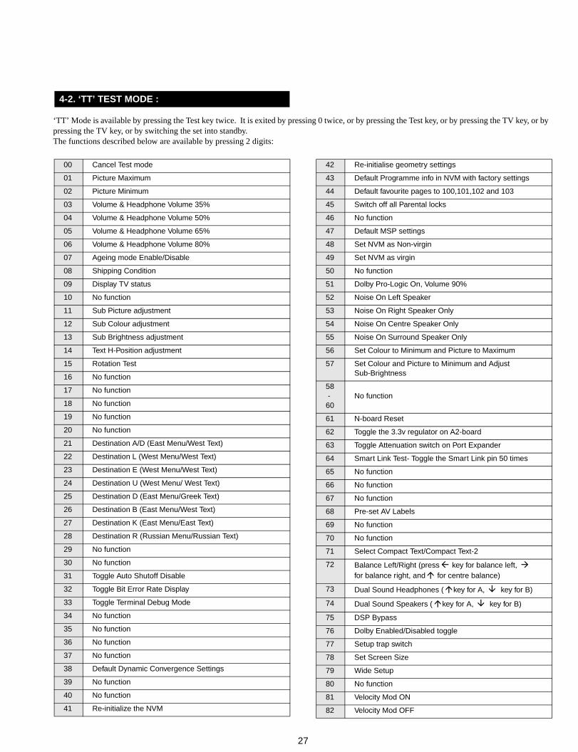
4-2. ‘TT’ TEST MODE :
00 Cancel Test mode
01 Picture Maximum
02 Picture Minimum
03 Volume & Headphone Volume 35%
04 Volume & Headphone Volume 50%
05 Volume & Headphone Volume 65%
06 Volume & Headphone Volume 80%
07 Ageing mode Enable/Disable
08 Shipping Condition
09 Display TV status
10 No function
11 Sub Picture adjustment
12 Sub Colour adjustment
13 Sub Brightness adjustment
14 Text H-Position adjustment
15 Rotation Test
16 No function
17 No function
18 No function
19 No function
20 No function
21 Destination A/D (East Menu/West Text)
22 Destination L (West Menu/West Text)
23 Destination E (West Menu/West Text)
24 Destination U (West Menu/ West Text)
25 Destination D (East Menu/Greek Text)
26 Destination B (East Menu/West Text)
27 Destination K (East Menu/East Text)
28 Destination R (Russian Menu/Russian Text)
29 No function
30 No function
31 Toggle Auto Shutoff Disable
32 Toggle Bit Error Rate Display
33 Toggle Terminal Debug Mode
34 No function
35 No function
36 No function
37 No function
38 Default Dynamic Convergence Settings
39 No function
40 No function
41 Re-initialize the NVM
42 Re-initialise geometry settings
43 Default Programme info in NVM with factory settings
44 Default favourite pages to 100,101,102 and 103
45 Switch off all Parental locks
46 No function
47 Default MSP settings
48 Set NVM as Non-virgin
49 Set NVM as virgin
50 No function
51 Dolby Pro-Logic On, Volume 90%
52 Noise On Left Speaker
53 Noise On Right Speaker Only
54 Noise On Centre Speaker Only
55 Noise On Surround Speaker Only
56 Set Colour to Minimum and Picture to Maximum
57 Set Colour and Picture to Minimum and Adjust Sub-Brightness
58 -60
No function
61 N-board Reset
62 Toggle the 3.3v regulator on A2-board
63 Toggle Attenuation switch on Port Expander
64 Smart Link Test- Toggle the Smart Link pin 50 times
65 No function
66 No function
67 No function
68 Pre-set AV Labels
69 No function
70 No function
71 Select Compact Text/Compact Text-2
72 Balance Left/Right (press � key for balance left, �for balance right, and � for centre balance)
73 Dual Sound Headphones ( �key for A, � key for B)
74 Dual Sound Speakers ( �key for A, � key for B)
75 DSP Bypass
76 Dolby Enabled/Disabled toggle
77 Setup trap switch
78 Set Screen Size
79 Wide Setup
80 No function
81 Velocity Mod ON
82 Velocity Mod OFF
‘TT’ Mode is available by pressing the Test key twice. It is exited by pressing 0 twice, or by pressing the Test key, or by pressing the TV key, or by pressing the TV key, or by switching the set into standby.The functions described below are available by pressing 2 digits:
27
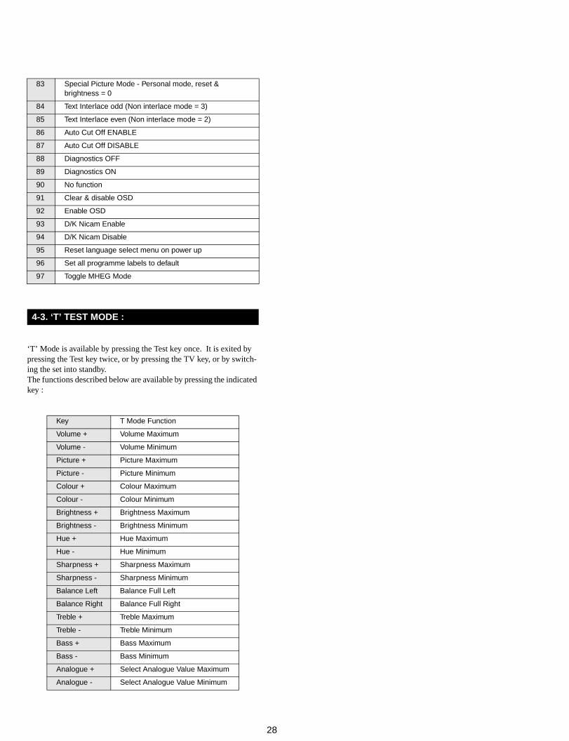
83 Special Picture Mode - Personal mode, reset & brightness = 0
84 Text Interlace odd (Non interlace mode = 3)
85 Text Interlace even (Non interlace mode = 2)
86 Auto Cut Off ENABLE
87 Auto Cut Off DISABLE
88 Diagnostics OFF
89 Diagnostics ON
90 No function
91 Clear & disable OSD
92 Enable OSD
93 D/K Nicam Enable
94 D/K Nicam Disable
95 Reset language select menu on power up
96 Set all programme labels to default
97 Toggle MHEG Mode
4-3. ‘T’ TEST MODE :
Key T Mode Function
Volume + Volume Maximum
Volume - Volume Minimum
Picture + Picture Maximum
Picture - Picture Minimum
Colour + Colour Maximum
Colour - Colour Minimum
Brightness + Brightness Maximum
Brightness - Brightness Minimum
Hue + Hue Maximum
Hue - Hue Minimum
Sharpness + Sharpness Maximum
Sharpness - Sharpness Minimum
Balance Left Balance Full Left
Balance Right Balance Full Right
Treble + Treble Maximum
Treble - Treble Minimum
Bass + Bass Maximum
Bass - Bass Minimum
Analogue + Select Analogue Value Maximum
Analogue - Select Analogue Value Minimum
‘T’ Mode is available by pressing the Test key once. It is exited by pressing the Test key twice, or by pressing the TV key, or by switch-ing the set into standby.The functions described below are available by pressing the indicated key :
28
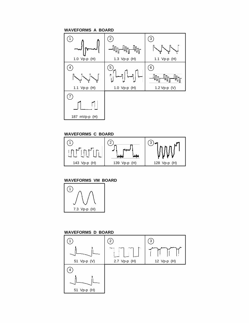
143 Vp-p (H)
1
139 Vp-p (H)
WAVEFORMS C BOARD
128 Vp-p (H)
32
7.3 Vp-p (H)
WAVEFORMS VM BOARD
1
1.1 Vp-p (H) 1.0 Vp-p (H)
5
1.0 Vp-p (H)
1
1.3 Vp-p (H)
2
WAVEFORMS A BOARD
187 mVp-p (H)
7
1.1 Vp-p (H)
1.2 Vp-p (V)
6
3
4
51 Vp-p (H)
51 Vp-p (V)
1
2.7 Vp-p (H)
2
WAVEFORMS D BOARD
12 Vp-p (H)
3
4
69
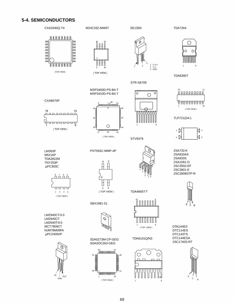
5-4. SEMICONDUCTORS
(TOP VIEW)
8 7 6 5
1 3 4
( TOP VIEW )
2
IN
GNDOUT
( TOP VIEW )
68 61
60
1
52
44
433527
26
18
10
9
4
1 2
3
( TOP VIEW )
( TOP VIEW )
1 20
21
40
4160
61
80
1 23
1 V OUT
2 V IN3 GND
1 9
23
567
1
4
( TOP VIEW )1 8
16 9
1 10
1120
( TOP VIEW )
E C B
CXA2040Q-T4
LM393PM5216PTDA2822MTNY253PµPC393C
LM2940CT-5.0LM2940CTLM2940T-9.0MCT7809CTNJM78M09FAµPC2405HF
PST593C-MMP-4P
MSP3400D-PS-B4-TMSP3410D-PS-B4-T
SBX1981-51
SDA5273M-CP-GEGSDA3OC263-GEG
SE135N
STR-S6709
STV9379
TDA7264
TDA8395T
2SA733-K2SA933AS2SA933S2SA1091-O2SC3502-EF2SC3601-E2SC2808STP-R
TDA4665T-T
1 8
1
2 3
4
TLP721(D4-)
30
1 9
TDA6101Q/N3
M24C332-MW6T
CXA8070P
EC B
DTA144ESDTC114ESDTC143TSDTC144ESA2SC1740S-RT
70
ECB
EC B
BE
C
B
C E
E CB
CATHODE
ANODE
CATHODE
ANODE
1
23
1 2 3
CATHODE
ANODE
CATHODE
ANODE
2SC2785-HFE
2SA1837
2SC2688-LK2SC3840(3)
2SC4793
2SC4927-01
EG-1Z-V1EGP20GEL1ZEM1-V1EU-1-V1EU2AEU2-V1FML-G12SGP08D
BAS216DTZ6.8CDTZ9.1DTZ33BRD5.65-B
D4SB60L
FMS-3FU
ERA38-06TP1HZS9.INB2MTZJ-3.6AMTZJ-5.1BMTZJ-5.6BMTZJ-6.8CMTZJ-9.1MTZJ-T-77-9.1AMTZJ-77-22B
HSS83TDRGP10GPKG23RGP15GPKG23
MA83301SS355TE-17UDZ-TE-17-5.6BHDZ-TE-17-6.8BUDZ-TE-17-9.1B
RD3.9ESB2RD5.1ESB2RD5.6ESB2RD6.8ESB2RD10ESB2RD15ES-B2RD39ES-B21SS133T-77
SLA-570KT3F
C
B
E
DTC144EKA2SA1037K2SA1162-G2SC2412K
3
21
2 3 1
NC
B
C E
IRF620
MA3030-H (TX)
71
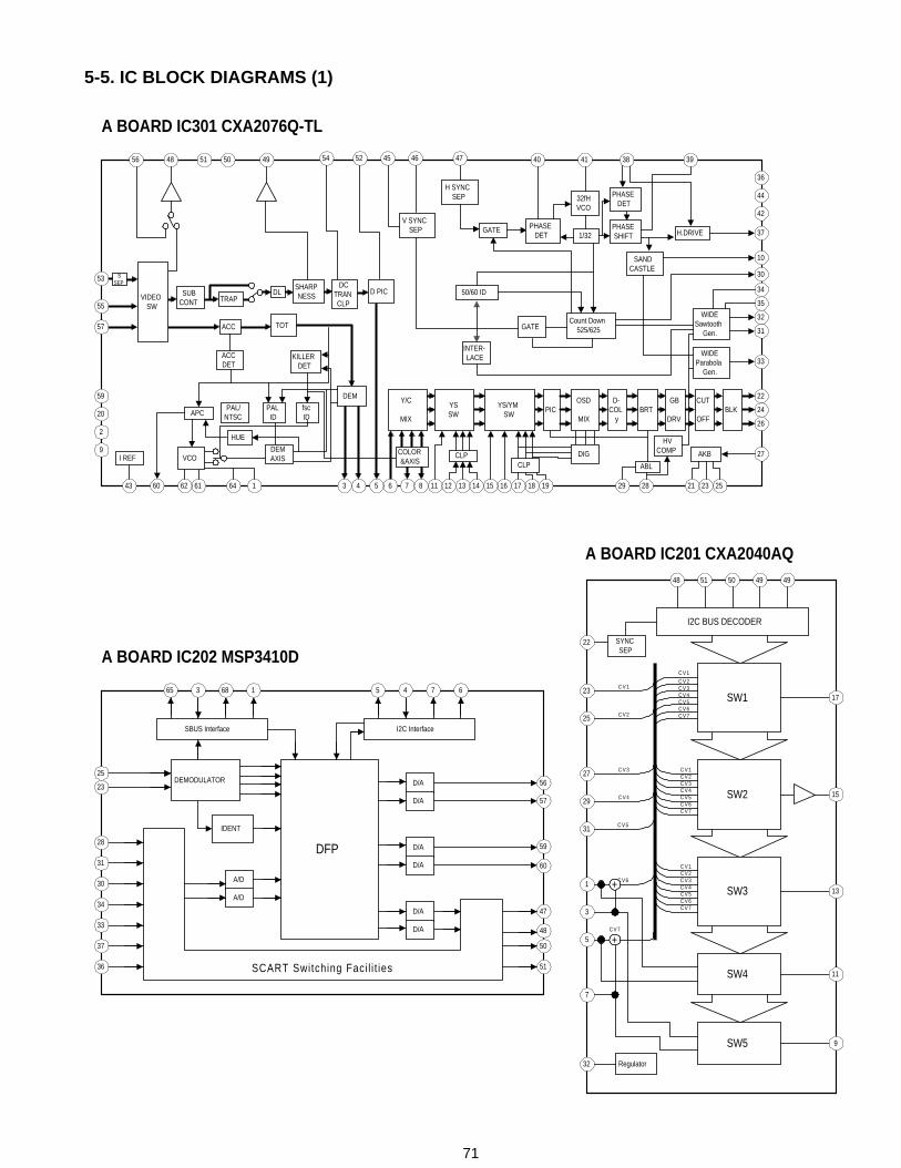
5-5. IC BLOCK DIAGRAMS (1)
56 48
ACCDET
KILLERDET
V SYNCSEP GATE
1/32
50/60 ID
GATE
SANDCASTLE
H.DRIVE
WIDESawtooth
Gen.
INTER-LACE
APCPAL/
NTSCfscID
I REF
HUE
CLPCLP ABL
HVCOMP AKB
51 50 49 54 52 45 46 47 40 41 39
36
44
42
10
35
30
34
32
31
33
27
2523282919181716151211164616260
9
2
20
59
37
WIDEParabola
Gen.
38
Count Down525/625
21141387654343
DLSUBCONT TRAP
ACC
55
57
SHARPNESS
PALID
DEM
TOT
DEMAXISVCO
VIDEOSW
53
PIC
22
24
26
PHASEDET
PHASESHIFT
PHASEDET
H SYNCSEP 32fH
VCO
YSSW
YS/YMSW
SSEP DC
TRANCLP
OSD
MIX
D-COL
yBRT
GB
DRV
CUT
OFFBLK
DIG
Y/C
MIX
COLOR&AXIS
A BOARD IC301 CXA2076Q-TL
D PIC
DFP60
59
56
57
SBUS Interface
IDENT
A/D
SCART Switching Faci l i t ies
A/D
D/A
D/A
D/A
D/A
D/A
D/A
I2C Interface
25
23
65 68 13 45 7 6
48
50
51
47
30
34
31
28
33
37
36
A BOARD IC202 MSP3410D
DEMODULATOR
22
48 51 50 49
I2C BUS DECODER
49
SW4
SW5
23
25
29
3
SYNCSEP
C V 2C V 3C V 4C V 5C V 6C V 7
C V 7C V 6C V 5C V 4C V 3C V 2C V 1
C V 7C V 6C V 5C V 4C V 3C V 2C V 1
SW2
SW3
SW1C V 1
C V 5
27
31
C V 2
C V 3
C V 4
C V 6
Regulator
1 +
+
C V 1
15
13
7
32
11
9
17
C V 7
5
A BOARD IC201 CXA2040AQ
D BOARD IC
6
4
7
8
72
5-5. IC BLOCK DIAGRAMS (2)
A BOARD IC4 PST593C
OSC
3
1
4
2
DELAYT
R
Q
Vcc
V out
G N D
Reset
+
-
D BOARD IC500 STV9379
+
-
THERMALPROTECTION
1POWER
AMP7
5
4
682
FLYBACKGENERATOR
D BOARD IC600 STR-S6709
PRE REG
START UP OVP
REF
1
2
87
PROPORTIONALDRIVE 5
4
3
6
OSC
THERMAL
LATCH
9
73
SECTION 6EXPLODED VIEWS
REF. NO. PART.NO DESCRIPTION REMARK REF. NO. PART.NO DESCRIPTION REMARK
• Items with no part number and no description are not stocked because they are seldom required for routine service.
• The construction parts of an assembled part are indi-cated with a collation number in the remarks column.
• Items marked “ * “ are not stockedsince they are seldom required forroutine service. Some delay shouldbe anticipated when ordering these items.
6-1. CHASSIS
NOTE :
1 *A-1646-183-A H BOARD, COMPLETE2 £ 1-571-433-21 SWITCH, PUSH (AC POWER)3 *4-204-752-01 BRACKET, MAIN4 *A-1640-350-A D1 BOARD, COMPLETE5 *4-202-531-01 AC CORD LOCK (SC)6 £ 1-783-083-11 CORD POWER (WITH NOISE FILTER)
(KV-32FX20A/32FX20B/32FX20D/32FX20E) £ 1-776-204-12 CORD POWER (FILTER) (KV-32FX20U)7 £ X-4560-158-1 TRANSFORMER ASSY, FLYBACK (NX-4404//U2B4)8 *A-1642-252-A D BOARD, COMPLETE9 *A-1642-251-A D2 BOARD, COMPLETE10 1-693-338-11 TUNER/VIF (AEP)(KV-32FX20A/32FX20D/
KV-32FX20E) 1-693-340-11 TUNER/VIF (FR) (KV-32FX20B) 1-693-339-11 TUNER/VIF (UK) (KV-32FX20U)
11 *A-1632-848-A A BOARD, COMPLETE (KV-32FX20A)*A-1632-847-A A BOARD, COMPLETE (KV-32FX20B)*A-1632-846-A A BOARD, COMPLETE (KV-32FX20D)*A-1632-849-A A BOARD, COMPLETE (KV-32FX20E)*A-1632-850-A A BOARD, COMPLETE (KV-32FX20U)
12 *A-1674-139-A SP BLOCK ASSY 13-1613 *4-204-776-11 BOX, WOOFER14 4-039-358-01 SCREW (4x16), (+) BV TAPPING15 1-529-417-11 SPEAKER (8CM)16 4-204-775-11 BAFFLE WOOFER17 4-384-096-01 SCREW (4x16), TAPPING + P18 1-529-408-11 SPEAKER 4.2x24CM19 4-204-735-01 COVER, REAR
18
16
15
14
1
2
6
17 13
12
7
14
19
KV-32FX20U only
10
9 8
5 4
3 17
18
11
74
REF. NO. PART.NO DESCRIPTION REMARK REF. NO. PART.NO DESCRIPTION REMARK
6-2. PICTURE TUBE
51 X-4200-488-1 BEZNET ASSY 55-5952 4-045-250-01 DAMPER53 4-204-731-11 DOOR54 4-202-555-01 SHAFT DOOR55 4-042-192-11 CATCHER, PUSH56 4-204-730-11 WINDOW ORNAMENTAL57 4-204-728-01 BUTTON, POWER58 4-202-964-11 SPRING59 4-204-729-01 GUIDE LIGHT60 4-203-128-41 SHEET, BLOTTING61 £ 8-735-054-05 PICTURE TUBE (W76LLZ060X) (SD-302)62 £ 1-451-480-11 DEFLECTION YOKE (Y32RVC2)63 1-452-896-11 COIL, NA ROTATION (RT200)64 £ 8-453-011-11 NECK ASSY, NA299-M65 *A-1644-098-A VM BOARD, COMPLETE
66 *A-1638-126-A C BOARD, COMPLETE67 4-200-433-01 SPRING, EXTENSION68 £ 1-416-769-11 COIL, DEMAGNETIC69 *4-392-534-31 CUSHION DGC70 *4-059-569-01 HOLDER, DGC71 4-202-554-01 HOLDER, HV CABLE72 £ 1-251-807-11 CAP ASSY, HIGH VOLTAGE73 3-704-495-01 SPACER, DY74 4-204-225-01 PT-SCREW75 4-308-870-00 CLIP, LEAD WIRE76 1-452-094-00 MAGNET, ROTATABLE DISK; 15MM Ø77 1-425-032-00 MAGNET,DISK; 10MM Ø78 X-4387-214-1 PERMALLOY ASSY, CORRECTION79 3-701-007-00 BAND, BINDING
72
62
52
75
76
77 78
79
74
54 56 57 58
60
63 64
65
66
55
67
71
68
70
59
53
61
69
69
73
51
75
PARTS LISTING TABLE OF CONTENTS
Page
A BOARD COMMON Parts List : Parts common to all models listed in this manual ............................... 76
A BOARD VARIANT Parts List : Parts that belong only to the model specified
Model
KV-32FX20A/32FX20B/KV-32FX20D/32FX20E ................................................................................................... 82
KV-32FX20U ................................................................................................... 82
C BOARD COMPLETE Parts List : ................................................................................................... 82
D1 BOARD COMPLETE Parts List : ................................................................................................... 83
D2 BOARD COMPLETE Parts List : ................................................................................................... 85
D BOARD COMPLETE Parts List : ................................................................................................... 86
VM BOARD COMPLETE Parts List : ................................................................................................... 90
H BOARD COMPLETE Parts List : ................................................................................................... 92
MISCELLANEOUS : ................................................................................................... 93
ACCESSORIES AND PACKAGING MATERIALS : ................................................................................................... 93
Note : Refer to the designated variant parts list when seeking a part indicated by an asterisk (*)
Parts indicated (#) on the Schematic Diagram are not used in this model andtherefore do not appear in the Parts List.
SECTION 7ELECTRICAL PARTS LIST
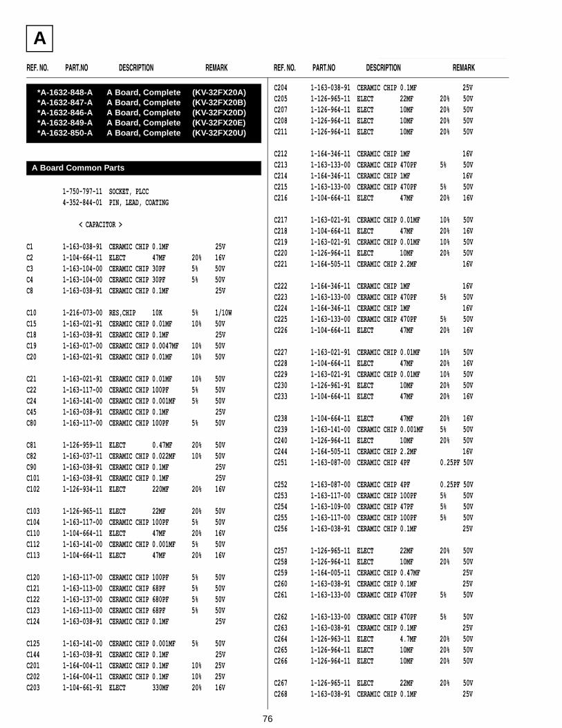
REF. NO. PART.NO DESCRIPTION REMARK REF. NO. PART.NO DESCRIPTION REMARK
The components identified byshading and marked are criticalfor safetyReplace only with the part numberspecified.
A
1-750-797-11 SOCKET, PLCC 4-352-844-01 PIN, LEAD, COATING
< CAPACITOR >
C1 1-163-038-91 CERAMIC CHIP 0.1MF 25VC2 1-104-664-11 ELECT 47MF 20% 16VC3 1-163-104-00 CERAMIC CHIP 30PF 5% 50VC4 1-163-104-00 CERAMIC CHIP 30PF 5% 50VC8 1-163-038-91 CERAMIC CHIP 0.1MF 25V
C10 1-216-073-00 RES,CHIP 10K 5% 1/10WC15 1-163-021-91 CERAMIC CHIP 0.01MF 10% 50VC18 1-163-038-91 CERAMIC CHIP 0.1MF 25VC19 1-163-017-00 CERAMIC CHIP 0.0047MF 10% 50VC20 1-163-021-91 CERAMIC CHIP 0.01MF 10% 50V
C21 1-163-021-91 CERAMIC CHIP 0.01MF 10% 50VC22 1-163-117-00 CERAMIC CHIP 100PF 5% 50VC24 1-163-141-00 CERAMIC CHIP 0.001MF 5% 50VC45 1-163-038-91 CERAMIC CHIP 0.1MF 25VC80 1-163-117-00 CERAMIC CHIP 100PF 5% 50V
C81 1-126-959-11 ELECT 0.47MF 20% 50VC82 1-163-037-11 CERAMIC CHIP 0.022MF 10% 50VC90 1-163-038-91 CERAMIC CHIP 0.1MF 25VC101 1-163-038-91 CERAMIC CHIP 0.1MF 25VC102 1-126-934-11 ELECT 220MF 20% 16V
C103 1-126-965-11 ELECT 22MF 20% 50VC104 1-163-117-00 CERAMIC CHIP 100PF 5% 50VC110 1-104-664-11 ELECT 47MF 20% 16VC112 1-163-141-00 CERAMIC CHIP 0.001MF 5% 50VC113 1-104-664-11 ELECT 47MF 20% 16V
C120 1-163-117-00 CERAMIC CHIP 100PF 5% 50VC121 1-163-113-00 CERAMIC CHIP 68PF 5% 50VC122 1-163-137-00 CERAMIC CHIP 680PF 5% 50VC123 1-163-113-00 CERAMIC CHIP 68PF 5% 50VC124 1-163-038-91 CERAMIC CHIP 0.1MF 25V
C125 1-163-141-00 CERAMIC CHIP 0.001MF 5% 50VC144 1-163-038-91 CERAMIC CHIP 0.1MF 25VC201 1-164-004-11 CERAMIC CHIP 0.1MF 10% 25VC202 1-164-004-11 CERAMIC CHIP 0.1MF 10% 25VC203 1-104-661-91 ELECT 330MF 20% 16V
C204 1-163-038-91 CERAMIC CHIP 0.1MF 25VC205 1-126-965-11 ELECT 22MF 20% 50VC207 1-126-964-11 ELECT 10MF 20% 50VC208 1-126-964-11 ELECT 10MF 20% 50VC211 1-126-964-11 ELECT 10MF 20% 50V
C212 1-164-346-11 CERAMIC CHIP 1MF 16VC213 1-163-133-00 CERAMIC CHIP 470PF 5% 50VC214 1-164-346-11 CERAMIC CHIP 1MF 16VC215 1-163-133-00 CERAMIC CHIP 470PF 5% 50VC216 1-104-664-11 ELECT 47MF 20% 16V
C217 1-163-021-91 CERAMIC CHIP 0.01MF 10% 50VC218 1-104-664-11 ELECT 47MF 20% 16VC219 1-163-021-91 CERAMIC CHIP 0.01MF 10% 50VC220 1-126-964-11 ELECT 10MF 20% 50VC221 1-164-505-11 CERAMIC CHIP 2.2MF 16V
C222 1-164-346-11 CERAMIC CHIP 1MF 16VC223 1-163-133-00 CERAMIC CHIP 470PF 5% 50VC224 1-164-346-11 CERAMIC CHIP 1MF 16VC225 1-163-133-00 CERAMIC CHIP 470PF 5% 50VC226 1-104-664-11 ELECT 47MF 20% 16V
C227 1-163-021-91 CERAMIC CHIP 0.01MF 10% 50VC228 1-104-664-11 ELECT 47MF 20% 16VC229 1-163-021-91 CERAMIC CHIP 0.01MF 10% 50VC230 1-126-961-91 ELECT 10MF 20% 50VC233 1-104-664-11 ELECT 47MF 20% 16V
C238 1-104-664-11 ELECT 47MF 20% 16VC239 1-163-141-00 CERAMIC CHIP 0.001MF 5% 50VC240 1-126-964-11 ELECT 10MF 20% 50VC244 1-164-505-11 CERAMIC CHIP 2.2MF 16VC251 1-163-087-00 CERAMIC CHIP 4PF 0.25PF 50V
C252 1-163-087-00 CERAMIC CHIP 4PF 0.25PF 50VC253 1-163-117-00 CERAMIC CHIP 100PF 5% 50VC254 1-163-109-00 CERAMIC CHIP 47PF 5% 50VC255 1-163-117-00 CERAMIC CHIP 100PF 5% 50VC256 1-163-038-91 CERAMIC CHIP 0.1MF 25V
C257 1-126-965-11 ELECT 22MF 20% 50VC258 1-126-964-11 ELECT 10MF 20% 50VC259 1-164-005-11 CERAMIC CHIP 0.47MF 25VC260 1-163-038-91 CERAMIC CHIP 0.1MF 25VC261 1-163-133-00 CERAMIC CHIP 470PF 5% 50V
C262 1-163-133-00 CERAMIC CHIP 470PF 5% 50VC263 1-163-038-91 CERAMIC CHIP 0.1MF 25VC264 1-126-963-11 ELECT 4.7MF 20% 50VC265 1-126-964-11 ELECT 10MF 20% 50VC266 1-126-964-11 ELECT 10MF 20% 50V
C267 1-126-965-11 ELECT 22MF 20% 50VC268 1-163-038-91 CERAMIC CHIP 0.1MF 25V
A Board Common Parts
*A-1632-848-A A Board, Complete (KV-32FX20A)*A-1632-847-A A Board, Complete (KV-32FX20B)*A-1632-846-A A Board, Complete (KV-32FX20D)*A-1632-849-A A Board, Complete (KV-32FX20E)*A-1632-850-A A Board, Complete (KV-32FX20U)
76
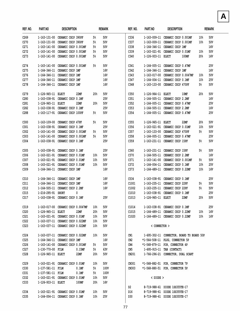
REF. NO. PART.NO DESCRIPTION REMARK REF. NO. PART.NO DESCRIPTION REMARK
The components identified byshading and marked are criticalfor safetyReplace only with the part numberspecified.
A
C269 1-163-131-00 CERAMIC CHIP 390PF 5% 50VC270 1-163-131-00 CERAMIC CHIP 390PF 5% 50VC271 1-163-141-00 CERAMIC CHIP 0.001MF 5% 50VC272 1-163-141-00 CERAMIC CHIP 0.001MF 5% 50VC273 1-163-141-00 CERAMIC CHIP 0.001MF 5% 50V
C274 1-163-141-00 CERAMIC CHIP 0.001MF 5% 50VC275 1-164-346-11 CERAMIC CHIP 1MF 16VC276 1-164-346-11 CERAMIC CHIP 1MF 16VC277 1-164-346-11 CERAMIC CHIP 1MF 16VC278 1-164-346-11 CERAMIC CHIP 1MF 16V
C279 1-126-965-11 ELECT 22MF 20% 50VC280 1-163-038-91 CERAMIC CHIP 0.1MF 25VC281 1-126-965-11 ELECT 22MF 20% 50VC282 1-163-038-91 CERAMIC CHIP 0.1MF 25VC288 1-163-117-91 CERAMIC CHIP 100PF 5% 50V
C300 1-163-109-00 CERAMIC CHIP 47PF 5% 50VC301 1-163-038-91 CERAMIC CHIP 0.1MF 25VC302 1-163-141-00 CERAMIC CHIP 0.001MF 5% 50VC303 1-163-141-00 CERAMIC CHIP 0.001MF 5% 50VC304 1-163-038-91 CERAMIC CHIP 0.1MF 25V
C305 1-163-038-91 CERAMIC CHIP 0.1MF 25VC306 1-163-021-91 CERAMIC CHIP 0.01MF 10% 50VC307 1-163-021-91 CERAMIC CHIP 0.01MF 10% 50VC308 1-163-021-91 CERAMIC CHIP 0.01MF 10% 50VC309 1-164-346-11 CERAMIC CHIP 1MF 16V
C310 1-164-346-11 CERAMIC CHIP 1MF 16VC311 1-164-346-11 CERAMIC CHIP 1MF 16VC312 1-164-505-11 CERAMIC CHIP 2.2MF 16VC315 1-216-295-91 SHORT 0C317 1-163-038-91 CERAMIC CHIP 0.1MF 25V
C319 1-163-017-00 CERAMIC CHIP 0.0047MF 10% 50VC320 1-126-965-11 ELECT 22MF 20% 50VC321 1-163-021-91 CERAMIC CHIP 0.01MF 10% 50VC322 1-163-037-11 CERAMIC CHIP 0.022MF 10% 50VC323 1-163-037-11 CERAMIC CHIP 0.022MF 10% 50V
C324 1-163-037-11 CERAMIC CHIP 0.022MF 10% 50VC325 1-164-346-11 CERAMIC CHIP 1MF 16VC326 1-163-141-00 CERAMIC CHIP 0.001MF 5% 50VC327 1-130-770-00 FILM 0.15MF 5% 63VC328 1-126-965-11 ELECT 22MF 20% 50V
C329 1-163-021-91 CERAMIC CHIP 0.01MF 10% 50VC330 1-137-581-11 FILM 0.1MF 5% 100VC331 1-137-581-11 FILM 0.1MF 5% 100VC332 1-163-021-91 CERAMIC CHIP 0.01MF 10% 50VC333 1-126-933-11 ELECT 100MF 20% 16V
C334 1-163-021-91 CERAMIC CHIP 0.01MF 10% 50VC335 1-164-004-11 CERAMIC CHIP 0.1MF 10% 25V
C336 1-163-009-11 CERAMIC CHIP 0.001MF 10% 50VC337 1-163-009-11 CERAMIC CHIP 0.001MF 10% 50VC338 1-164-346-11 CERAMIC CHIP 1MF 16VC339 1-163-021-91 CERAMIC CHIP 0.01MF 10% 50VC340 1-126-933-11 ELECT 100MF 20% 16V
C341 1-164-005-11 CERAMIC CHIP 0.47MF 25VC342 1-164-346-11 CERAMIC CHIP 1MF 16VC343 1-163-017-00 CERAMIC CHIP 0.0047MF 10% 50VC347 1-164-004-11 CERAMIC CHIP 0.1MF 10% 25VC348 1-163-133-00 CERAMIC CHIP 470PF 5% 50V
C350 1-126-964-11 ELECT 10MF 20% 50VC351 1-164-505-11 CERAMIC CHIP 2.2MF 16VC352 1-164-005-11 CERAMIC CHIP 0.47MF 25VC353 1-164-505-11 CERAMIC CHIP 2.2MF 16VC354 1-164-005-11 CERAMIC CHIP 0.47MF 25V
C355 1-126-965-11 ELECT 22MF 20% 50VC356 1-163-021-91 CERAMIC CHIP 0.01MF 10% 50VC357 1-163-133-00 CERAMIC CHIP 470PF 5% 50VC358 1-164-005-11 CERAMIC CHIP 0.47MF 25VC359 1-163-231-11 CERAMIC CHIP 15PF 5% 50V
C360 1-163-231-11 CERAMIC CHIP 15PF 5% 50VC370 1-164-505-11 CERAMIC CHIP 2.2MF 16VC371 1-163-141-00 CERAMIC CHIP 0.001MF 5% 50VC372 1-164-004-11 CERAMIC CHIP 0.1MF 10% 25VC373 1-164-489-11 CERAMIC CHIP 0.22MF 10% 16V
C534 1-163-038-91 CERAMIC CHIP 0.1MF 25VC1001 1-163-235-11 CERAMIC CHIP 22PF 5% 50VC1002 1-163-235-11 CERAMIC CHIP 22PF 5% 50VC1010 1-163-038-91 CERAMIC CHIP 0.1MF 25VC1013 1-126-965-11 ELECT 22MF 20% 50V
C1014 1-163-038-91 CERAMIC CHIP 0.1MF 25VC1015 1-164-489-11 CERAMIC CHIP 0.22MF 10% 16VC1020 1-164-489-11 CERAMIC CHIP 0.22MF 10% 16V
< CONNECTOR >
CN1 1-695-302-11 CONNECTOR, BOARD TO BOARD 50PCN2 *1-564-508-11 PLUG, CONNECTOR 5PCN4 *1-568-879-11 PIN, CONNECTOR 4PCN5 1-695-915-11 TAB (CONTACT)CN201 1-766-296-21 CONNECTOR, DUAL SCART
CN301 *1-568-882-51 PIN, CONNECTOR 7PCN303 *1-568-880-51 PIN, CONNECTOR 5P
< DIODE >
D2 8-719-988-61 DIODE 1SS355TE-17D16 8-719-988-61 DIODE 1SS355TE-17D30 8-719-988-61 DIODE 1SS355TE-17
77
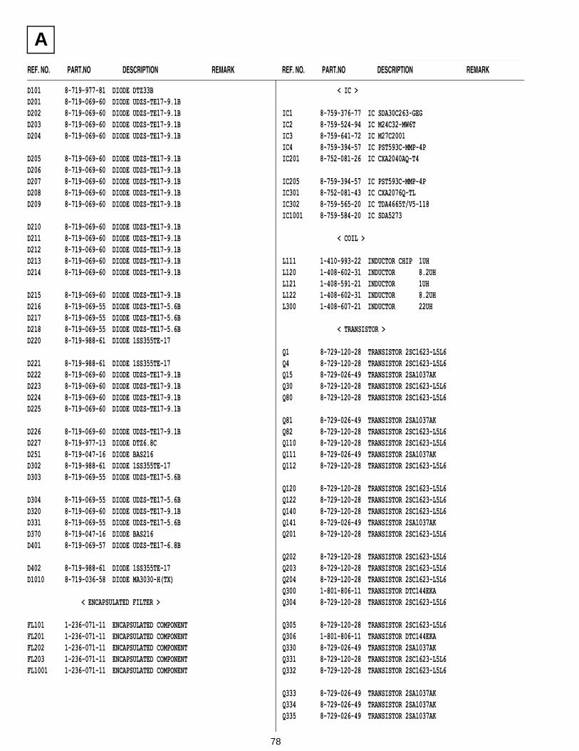
REF. NO. PART.NO DESCRIPTION REMARK REF. NO. PART.NO DESCRIPTION REMARK
The components identified byshading and marked are criticalfor safetyReplace only with the part numberspecified.
A
D101 8-719-977-81 DIODE DTZ33BD201 8-719-069-60 DIODE UDZS-TE17-9.1BD202 8-719-069-60 DIODE UDZS-TE17-9.1BD203 8-719-069-60 DIODE UDZS-TE17-9.1BD204 8-719-069-60 DIODE UDZS-TE17-9.1B
D205 8-719-069-60 DIODE UDZS-TE17-9.1BD206 8-719-069-60 DIODE UDZS-TE17-9.1BD207 8-719-069-60 DIODE UDZS-TE17-9.1BD208 8-719-069-60 DIODE UDZS-TE17-9.1BD209 8-719-069-60 DIODE UDZS-TE17-9.1B
D210 8-719-069-60 DIODE UDZS-TE17-9.1BD211 8-719-069-60 DIODE UDZS-TE17-9.1BD212 8-719-069-60 DIODE UDZS-TE17-9.1BD213 8-719-069-60 DIODE UDZS-TE17-9.1B D214 8-719-069-60 DIODE UDZS-TE17-9.1B
D215 8-719-069-60 DIODE UDZS-TE17-9.1BD216 8-719-069-55 DIODE UDZS-TE17-5.6BD217 8-719-069-55 DIODE UDZS-TE17-5.6BD218 8-719-069-55 DIODE UDZS-TE17-5.6BD220 8-719-988-61 DIODE 1SS355TE-17
D221 8-719-988-61 DIODE 1SS355TE-17D222 8-719-069-60 DIODE UDZS-TE17-9.1BD223 8-719-069-60 DIODE UDZS-TE17-9.1BD224 8-719-069-60 DIODE UDZS-TE17-9.1BD225 8-719-069-60 DIODE UDZS-TE17-9.1B
D226 8-719-069-60 DIODE UDZS-TE17-9.1BD227 8-719-977-13 DIODE DTZ6.8CD251 8-719-047-16 DIODE BAS216D302 8-719-988-61 DIODE 1SS355TE-17D303 8-719-069-55 DIODE UDZS-TE17-5.6B
D304 8-719-069-55 DIODE UDZS-TE17-5.6BD320 8-719-069-60 DIODE UDZS-TE17-9.1BD331 8-719-069-55 DIODE UDZS-TE17-5.6BD370 8-719-047-16 DIODE BAS216D401 8-719-069-57 DIODE UDZS-TE17-6.8B
D402 8-719-988-61 DIODE 1SS355TE-17D1010 8-719-036-58 DIODE MA3030-H(TX)
< ENCAPSULATED FILTER >
FL101 1-236-071-11 ENCAPSULATED COMPONENTFL201 1-236-071-11 ENCAPSULATED COMPONENTFL202 1-236-071-11 ENCAPSULATED COMPONENTFL203 1-236-071-11 ENCAPSULATED COMPONENTFL1001 1-236-071-11 ENCAPSULATED COMPONENT
< IC >
IC1 8-759-376-77 IC SDA30C263-GEGIC2 8-759-524-94 IC M24C32-MW6TIC3 8-759-641-72 IC M27C2001IC4 8-759-394-57 IC PST593C-MMP-4PIC201 8-752-081-26 IC CXA2040AQ-T4
IC205 8-759-394-57 IC PST593C-MMP-4PIC301 8-752-081-43 IC CXA2076Q-TLIC302 8-759-565-20 IC TDA4665T/V5-118IC1001 8-759-584-20 IC SDA5273
< COIL >
L111 1-410-993-22 INDUCTOR CHIP 1UHL120 1-408-602-31 INDUCTOR 8.2UHL121 1-408-591-21 INDUCTOR 1UHL122 1-408-602-31 INDUCTOR 8.2UHL300 1-408-607-21 INDUCTOR 22UH
< TRANSISTOR >
Q1 8-729-120-28 TRANSISTOR 2SC1623-L5L6Q4 8-729-120-28 TRANSISTOR 2SC1623-L5L6Q15 8-729-026-49 TRANSISTOR 2SA1037AKQ30 8-729-120-28 TRANSISTOR 2SC1623-L5L6Q80 8-729-120-28 TRANSISTOR 2SC1623-L5L6
Q81 8-729-026-49 TRANSISTOR 2SA1037AKQ82 8-729-120-28 TRANSISTOR 2SC1623-L5L6Q110 8-729-120-28 TRANSISTOR 2SC1623-L5L6Q111 8-729-026-49 TRANSISTOR 2SA1037AKQ112 8-729-120-28 TRANSISTOR 2SC1623-L5L6
Q120 8-729-120-28 TRANSISTOR 2SC1623-L5L6Q122 8-729-120-28 TRANSISTOR 2SC1623-L5L6Q140 8-729-120-28 TRANSISTOR 2SC1623-L5L6Q141 8-729-026-49 TRANSISTOR 2SA1037AKQ201 8-729-120-28 TRANSISTOR 2SC1623-L5L6
Q202 8-729-120-28 TRANSISTOR 2SC1623-L5L6Q203 8-729-120-28 TRANSISTOR 2SC1623-L5L6Q204 8-729-120-28 TRANSISTOR 2SC1623-L5L6Q300 1-801-806-11 TRANSISTOR DTC144EKAQ304 8-729-120-28 TRANSISTOR 2SC1623-L5L6
Q305 8-729-120-28 TRANSISTOR 2SC1623-L5L6Q306 1-801-806-11 TRANSISTOR DTC144EKAQ330 8-729-026-49 TRANSISTOR 2SA1037AKQ331 8-729-120-28 TRANSISTOR 2SC1623-L5L6Q332 8-729-120-28 TRANSISTOR 2SC1623-L5L6
Q333 8-729-026-49 TRANSISTOR 2SA1037AKQ334 8-729-026-49 TRANSISTOR 2SA1037AKQ335 8-729-026-49 TRANSISTOR 2SA1037AK
78
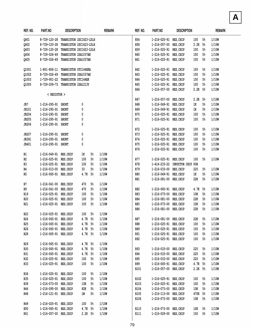
REF. NO. PART.NO DESCRIPTION REMARK REF. NO. PART.NO DESCRIPTION REMARK
The components identified byshading and marked are criticalfor safetyReplace only with the part numberspecified.
A
Q401 8-729-120-28 TRANSISTOR 2SC1623-L5L6Q402 8-729-120-28 TRANSISTOR 2SC1623-L5L6Q403 8-729-120-28 TRANSISTOR 2SC1623-L5L6Q404 8-729-026-49 TRANSISTOR 2SA1037AKQ405 8-729-026-49 TRANSISTOR 2SA1037AK
Q1001 1-801-806-11 TRANSISTOR DTC144EKAQ1002 8-729-026-49 TRANSISTOR 2SA1037AKQ1003 1-729-901-22 TRANSISTOR DTC144EKQ1005 8-729-209-73 TRANSISTOR 2SA1213Y
< RESISTOR >
JR7 1-216-295-91 SHORT 0JR101 1-216-295-91 SHORT 0JR204 1-216-295-91 SHORT 0JR205 1-216-295-91 SHORT 0JR206 1-216-295-91 SHORT 0
JR207 1-216-295-91 SHORT 0JR391 1-216-295-91 SHORT 0JR401 1-216-295-91 SHORT 0
R1 1-216-049-91 RES,CHIP 1K 5% 1/10WR2 1-216-025-91 RES,CHIP 100 5% 1/10WR3 1-216-025-91 RES,CHIP 100 5% 1/10WR4 1-216-013-00 RES,CHIP 33 5% 1/10WR5 1-216-065-91 RES,CHIP 4.7K 5% 1/10W
R7 1-216-041-00 RES,CHIP 470 5% 1/10WR9 1-216-041-00 RES,CHIP 470 5% 1/10WR19 1-216-025-91 RES,CHIP 100 5% 1/10WR20 1-216-025-91 RES,CHIP 100 5% 1/10WR21 1-216-025-91 RES,CHIP 100 5% 1/10W
R22 1-216-025-91 RES,CHIP 100 5% 1/10WR24 1-216-065-91 RES,CHIP 4.7K 5% 1/10WR25 1-216-065-91 RES,CHIP 4.7K 5% 1/10WR26 1-216-065-91 RES,CHIP 4.7K 5% 1/10WR28 1-216-065-91 RES,CHIP 4.7K 5% 1/10W
R29 1-216-065-91 RES,CHIP 4.7K 5% 1/10WR30 1-216-065-91 RES,CHIP 4.7K 5% 1/10WR31 1-216-065-91 RES,CHIP 4.7K 5% 1/10WR32 1-216-025-91 RES,CHIP 100 5% 1/10WR33 1-216-025-91 RES,CHIP 100 5% 1/10W
R34 1-216-025-91 RES,CHIP 100 5% 1/10WR35 1-216-025-91 RES,CHIP 100 5% 1/10WR39 1-216-073-00 RES,CHIP 10K 5% 1/10WR46 1-216-095-00 RES,CHIP 82K 5% 1/10WR48 1-216-121-91 RES,CHIP 1M 5% 1/10W
R49 1-216-025-91 RES,CHIP 100 5% 1/10WR50 1-216-065-91 RES,CHIP 4.7K 5% 1/10WR51 1-216-057-00 RES,CHIP 2.2K 5% 1/10W
R54 1-216-025-91 RES,CHIP 100 5% 1/10WR58 1-216-057-00 RES,CHIP 2.2K 5% 1/10WR59 1-216-025-91 RES,CHIP 100 5% 1/10WR60 1-216-025-91 RES,CHIP 100 5% 1/10WR61 1-216-025-91 RES,CHIP 100 5% 1/10W
R62 1-216-025-91 RES,CHIP 100 5% 1/10WR63 1-216-025-91 RES,CHIP 100 5% 1/10WR64 1-216-025-91 RES,CHIP 100 5% 1/10WR65 1-216-025-91 RES,CHIP 100 5% 1/10WR66 1-216-057-00 RES,CHIP 2.2K 5% 1/10W
R67 1-216-057-00 RES,CHIP 2.2K 5% 1/10WR68 1-216-049-91 RES,CHIP 1K 5% 1/10WR69 1-216-049-91 RES,CHIP 1K 5% 1/10WR70 1-216-025-91 RES,CHIP 100 5% 1/10WR71 1-216-025-91 RES,CHIP 100 5% 1/10W
R72 1-216-025-91 RES,CHIP 100 5% 1/10WR73 1-216-025-91 RES,CHIP 100 5% 1/10WR74 1-216-025-91 RES,CHIP 100 5% 1/10WR75 1-216-025-91 RES,CHIP 100 5% 1/10WR76 1-216-025-91 RES,CHIP 100 5% 1/10W
R77 1-216-025-91 RES,CHIP 100 5% 1/10WR78 1-414-233-22 INDUCTOR CHIP 0UHR79 1-216-033-00 RES,CHIP 220 5% 1/10WR80 1-216-049-91 RES,CHIP 1K 5% 1/10WR81 1-216-081-00 RES,CHIP 22K 5% 1/10W
R82 1-216-065-91 RES,CHIP 4.7K 5% 1/10WR83 1-216-073-00 RES,CHIP 10K 5% 1/10WR84 1-216-081-00 RES,CHIP 22K 5% 1/10WR85 1-216-073-00 RES,CHIP 10K 5% 1/10WR86 1-216-081-00 RES,CHIP 22K 5% 1/10W
R87 1-216-081-00 RES,CHIP 22K 5% 1/10WR88 1-216-025-91 RES,CHIP 100 5% 1/10WR89 1-216-025-91 RES,CHIP 100 5% 1/10WR91 1-216-025-91 RES,CHIP 100 5% 1/10WR92 1-216-025-91 RES,CHIP 100 5% 1/10W
R93 1-216-033-00 RES,CHIP 220 5% 1/10WR94 1-216-033-00 RES,CHIP 220 5% 1/10WR95 1-216-033-00 RES,CHIP 220 5% 1/10WR99 1-216-065-91 RES,CHIP 4.7K 5% 1/10WR101 1-216-057-00 RES,CHIP 2.2K 5% 1/10W
R102 1-216-025-91 RES,CHIP 100 5% 1/10WR103 1-216-025-91 RES,CHIP 100 5% 1/10WR104 1-216-073-00 RES,CHIP 10K 5% 1/10WR105 1-216-113-00 RES,CHIP 470K 5% 1/10WR106 1-216-073-00 RES,CHIP 10K 5% 1/10W
R110 1-216-073-00 RES,CHIP 10K 5% 1/10WR111 1-216-029-00 RES,CHIP 150 5% 1/10W
79

REF. NO. PART.NO DESCRIPTION REMARK REF. NO. PART.NO DESCRIPTION REMARK
The components identified byshading and marked are criticalfor safetyReplace only with the part numberspecified.
A
R112 1-216-029-00 RES,CHIP 150 5% 1/10WR113 1-216-001-00 RES,CHIP 10 5% 1/10WR114 1-216-029-00 RES,CHIP 150 5% 1/10WR115 1-216-033-00 RES,CHIP 220 5% 1/10WR116 1-216-025-91 RES,CHIP 100 5% 1/10W
R117 1-216-065-91 RES,CHIP 4.7K 5% 1/10WR118 1-216-097-91 RES,CHIP 100K 5% 1/10WR120 1-216-069-00 RES,CHIP 6.8K 5% 1/10WR121 1-216-073-00 RES,CHIP 10K 5% 1/10WR122 1-216-041-00 RES,CHIP 470 5% 1/10W
R123 1-216-031-00 RES,CHIP 180 5% 1/10WR124 1-216-049-91 RES,CHIP 1K 5% 1/10WR125 1-216-081-00 RES,CHIP 22K 5% 1/10WR126 1-216-025-91 RES,CHIP 100 5% 1/10WR127 1-216-081-00 RES,CHIP 22K 5% 1/10W
R128 1-216-035-00 RES,CHIP 270 5% 1/10WR129 1-216-033-00 RES,CHIP 220 5% 1/10WR130 1-216-061-00 RES,CHIP 3.3K 5% 1/10WR131 1-216-073-00 RES,CHIP 10K 5% 1/10WR132 1-216-025-91 RES,CHIP 100 5% 1/10W
R133 1-216-041-00 RES,CHIP 470 5% 1/10WR134 1-216-001-00 RES,CHIP 10 5% 1/10WR135 1-216-037-00 RES,CHIP 330 5% 1/10WR136 1-216-033-00 RES,CHIP 220 5% 1/10WR137 1-216-049-91 RES,CHIP 1K 5% 1/10W
R138 1-216-041-00 RES,CHIP 470 5% 1/10WR144 1-216-081-00 RES,CHIP 22K 5% 1/10WR145 1-216-049-91 RES,CHIP 1K 5% 1/10WR146 1-216-049-91 RES,CHIP 1K 5% 1/10WR147 1-216-033-00 RES,CHIP 220 5% 1/10W
R148 1-216-051-00 RES,CHIP 1.2K 5% 1/10WR149 1-216-049-91 RES,CHIP 1K 5% 1/10WR150 1-216-061-00 RES,CHIP 3.3K 5% 1/10WR151 1-216-025-91 RES,CHIP 100 5% 1/10WR153 1-216-295-91 SHORT 0
R200 1-216-049-91 RES,CHIP 1K 5% 1/10WR203 1-216-025-91 RES,CHIP 100 5% 1/10WR204 1-216-025-91 RES,CHIP 100 5% 1/10WR205 1-216-081-00 RES,CHIP 22K 5% 1/10WR206 1-216-033-00 RES,CHIP 220 5% 1/10W
R208 1-216-041-00 RES,CHIP 470 5% 1/10WR209 1-216-182-00 RES,CHIP 220 5% 1/8WR210 1-216-017-91 RES,CHIP 47 5% 1/10WR211 1-216-033-00 RES,CHIP 220 5% 1/10WR212 1-216-022-00 RES,CHIP 75 5% 1/10W
R213 1-216-022-00 RES,CHIP 75 5% 1/10WR214 1-216-025-91 RES,CHIP 100 5% 1/10W
R216 1-216-025-91 RES,CHIP 100 5% 1/10WR217 1-216-113-00 RES,CHIP 470K 5% 1/10WR218 1-216-025-91 RES,CHIP 100 5% 1/10WR219 1-216-113-00 RES,CHIP 470K 5% 1/10WR220 1-216-295-91 SHORT 0
R221 1-216-041-00 RES,CHIP 470 5% 1/10WR222 1-216-089-91 RES,CHIP 47K 5% 1/10WR223 1-216-295-91 SHORT 0R224 1-216-041-00 RES,CHIP 470 5% 1/10WR225 1-216-089-91 RES,CHIP 47K 5% 1/10W
R226 1-216-033-00 RES,CHIP 220 5% 1/10WR227 1-216-022-00 RES,CHIP 75 5% 1/10WR228 1-216-022-00 RES,CHIP 75 5% 1/10WR229 1-216-033-00 RES,CHIP 220 5% 1/10WR230 1-216-022-00 RES,CHIP 75 5% 1/10W
R232 1-216-025-91 RES,CHIP 100 5% 1/10WR233 1-216-025-91 RES,CHIP 100 5% 1/10WR234 1-216-113-00 RES,CHIP 470K 5% 1/10WR235 1-216-025-91 RES,CHIP 100 5% 1/10WR236 1-216-113-00 RES,CHIP 470K 5% 1/10W
R237 1-216-295-91 SHORT 0R238 1-216-089-91 RES,CHIP 47K 5% 1/10WR239 1-216-041-00 RES,CHIP 470 5% 1/10WR240 1-216-295-91 SHORT 0R241 1-216-089-91 RES,CHIP 47K 5% 1/10W
R242 1-216-041-00 RES,CHIP 470 5% 1/10WR243 1-216-033-00 RES,CHIP 220 5% 1/10WR244 1-216-033-00 RES,CHIP 220 5% 1/10WR249 1-216-001-00 RES,CHIP 10 5% 1/10WR255 1-216-025-91 RES,CHIP 100 5% 1/10W
R256 1-216-025-91 RES,CHIP 100 5% 1/10WR257 1-216-017-91 RES,CHIP 47 5% 1/10WR258 1-216-049-91 RES,CHIP 1K 5% 1/10WR259 1-216-033-00 RES,CHIP 220 5% 1/10WR260 1-216-033-00 RES,CHIP 220 5% 1/10W
R261 1-216-022-00 RES,CHIP 75 5% 1/10WR265 1-216-065-91 RES,CHIP 4.7K 5% 1/10WR266 1-216-295-91 SHORT 0R267 1-216-295-91 SHORT 0R270 1-216-022-00 RES,CHIP 75 5% 1/10W
R271 1-216-022-00 RES,CHIP 75 5% 1/10WR272 1-216-022-00 RES,CHIP 75 5% 1/10WR273 1-216-022-00 RES,CHIP 75 5% 1/10WR274 1-216-295-91 SHORT 0R275 1-216-295-91 SHORT 0
R276 1-216-295-91 SHORT 0R277 1-216-295-91 SHORT 0
80
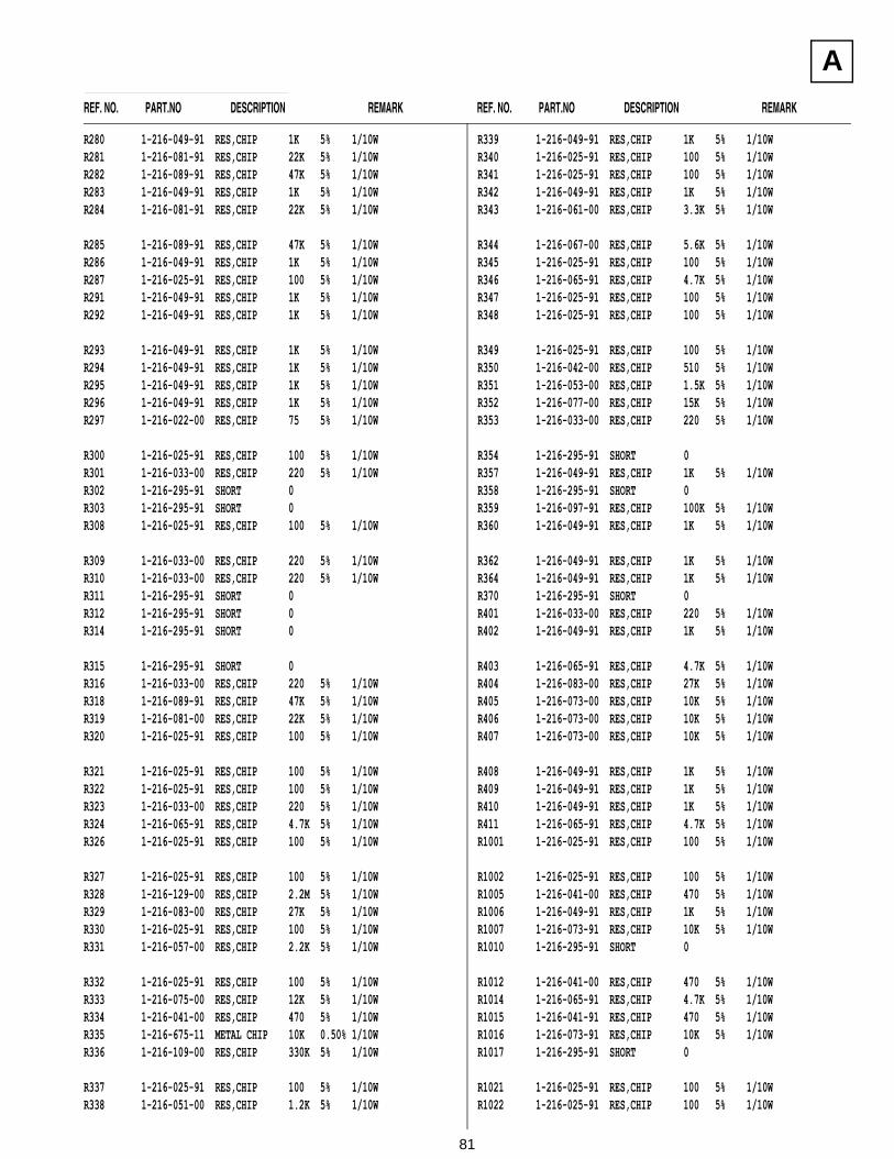
REF. NO. PART.NO DESCRIPTION REMARK REF. NO. PART.NO DESCRIPTION REMARK
The components identified byshading and marked are criticalfor safetyReplace only with the part numberspecified.
A
R280 1-216-049-91 RES,CHIP 1K 5% 1/10WR281 1-216-081-91 RES,CHIP 22K 5% 1/10WR282 1-216-089-91 RES,CHIP 47K 5% 1/10WR283 1-216-049-91 RES,CHIP 1K 5% 1/10WR284 1-216-081-91 RES,CHIP 22K 5% 1/10W
R285 1-216-089-91 RES,CHIP 47K 5% 1/10WR286 1-216-049-91 RES,CHIP 1K 5% 1/10WR287 1-216-025-91 RES,CHIP 100 5% 1/10WR291 1-216-049-91 RES,CHIP 1K 5% 1/10WR292 1-216-049-91 RES,CHIP 1K 5% 1/10W
R293 1-216-049-91 RES,CHIP 1K 5% 1/10WR294 1-216-049-91 RES,CHIP 1K 5% 1/10WR295 1-216-049-91 RES,CHIP 1K 5% 1/10WR296 1-216-049-91 RES,CHIP 1K 5% 1/10WR297 1-216-022-00 RES,CHIP 75 5% 1/10W
R300 1-216-025-91 RES,CHIP 100 5% 1/10WR301 1-216-033-00 RES,CHIP 220 5% 1/10WR302 1-216-295-91 SHORT 0R303 1-216-295-91 SHORT 0R308 1-216-025-91 RES,CHIP 100 5% 1/10W
R309 1-216-033-00 RES,CHIP 220 5% 1/10WR310 1-216-033-00 RES,CHIP 220 5% 1/10WR311 1-216-295-91 SHORT 0R312 1-216-295-91 SHORT 0R314 1-216-295-91 SHORT 0
R315 1-216-295-91 SHORT 0R316 1-216-033-00 RES,CHIP 220 5% 1/10WR318 1-216-089-91 RES,CHIP 47K 5% 1/10WR319 1-216-081-00 RES,CHIP 22K 5% 1/10WR320 1-216-025-91 RES,CHIP 100 5% 1/10W
R321 1-216-025-91 RES,CHIP 100 5% 1/10WR322 1-216-025-91 RES,CHIP 100 5% 1/10WR323 1-216-033-00 RES,CHIP 220 5% 1/10WR324 1-216-065-91 RES,CHIP 4.7K 5% 1/10WR326 1-216-025-91 RES,CHIP 100 5% 1/10W
R327 1-216-025-91 RES,CHIP 100 5% 1/10WR328 1-216-129-00 RES,CHIP 2.2M 5% 1/10WR329 1-216-083-00 RES,CHIP 27K 5% 1/10WR330 1-216-025-91 RES,CHIP 100 5% 1/10WR331 1-216-057-00 RES,CHIP 2.2K 5% 1/10W
R332 1-216-025-91 RES,CHIP 100 5% 1/10WR333 1-216-075-00 RES,CHIP 12K 5% 1/10WR334 1-216-041-00 RES,CHIP 470 5% 1/10WR335 1-216-675-11 METAL CHIP 10K 0.50% 1/10WR336 1-216-109-00 RES,CHIP 330K 5% 1/10W
R337 1-216-025-91 RES,CHIP 100 5% 1/10WR338 1-216-051-00 RES,CHIP 1.2K 5% 1/10W
R339 1-216-049-91 RES,CHIP 1K 5% 1/10WR340 1-216-025-91 RES,CHIP 100 5% 1/10WR341 1-216-025-91 RES,CHIP 100 5% 1/10WR342 1-216-049-91 RES,CHIP 1K 5% 1/10WR343 1-216-061-00 RES,CHIP 3.3K 5% 1/10W
R344 1-216-067-00 RES,CHIP 5.6K 5% 1/10WR345 1-216-025-91 RES,CHIP 100 5% 1/10WR346 1-216-065-91 RES,CHIP 4.7K 5% 1/10WR347 1-216-025-91 RES,CHIP 100 5% 1/10WR348 1-216-025-91 RES,CHIP 100 5% 1/10W
R349 1-216-025-91 RES,CHIP 100 5% 1/10WR350 1-216-042-00 RES,CHIP 510 5% 1/10WR351 1-216-053-00 RES,CHIP 1.5K 5% 1/10WR352 1-216-077-00 RES,CHIP 15K 5% 1/10WR353 1-216-033-00 RES,CHIP 220 5% 1/10W
R354 1-216-295-91 SHORT 0R357 1-216-049-91 RES,CHIP 1K 5% 1/10WR358 1-216-295-91 SHORT 0R359 1-216-097-91 RES,CHIP 100K 5% 1/10WR360 1-216-049-91 RES,CHIP 1K 5% 1/10W
R362 1-216-049-91 RES,CHIP 1K 5% 1/10WR364 1-216-049-91 RES,CHIP 1K 5% 1/10WR370 1-216-295-91 SHORT 0R401 1-216-033-00 RES,CHIP 220 5% 1/10WR402 1-216-049-91 RES,CHIP 1K 5% 1/10W
R403 1-216-065-91 RES,CHIP 4.7K 5% 1/10WR404 1-216-083-00 RES,CHIP 27K 5% 1/10WR405 1-216-073-00 RES,CHIP 10K 5% 1/10WR406 1-216-073-00 RES,CHIP 10K 5% 1/10WR407 1-216-073-00 RES,CHIP 10K 5% 1/10W
R408 1-216-049-91 RES,CHIP 1K 5% 1/10WR409 1-216-049-91 RES,CHIP 1K 5% 1/10WR410 1-216-049-91 RES,CHIP 1K 5% 1/10WR411 1-216-065-91 RES,CHIP 4.7K 5% 1/10WR1001 1-216-025-91 RES,CHIP 100 5% 1/10W
R1002 1-216-025-91 RES,CHIP 100 5% 1/10WR1005 1-216-041-00 RES,CHIP 470 5% 1/10WR1006 1-216-049-91 RES,CHIP 1K 5% 1/10WR1007 1-216-073-91 RES,CHIP 10K 5% 1/10WR1010 1-216-295-91 SHORT 0
R1012 1-216-041-00 RES,CHIP 470 5% 1/10WR1014 1-216-065-91 RES,CHIP 4.7K 5% 1/10WR1015 1-216-041-91 RES,CHIP 470 5% 1/10WR1016 1-216-073-91 RES,CHIP 10K 5% 1/10WR1017 1-216-295-91 SHORT 0
R1021 1-216-025-91 RES,CHIP 100 5% 1/10WR1022 1-216-025-91 RES,CHIP 100 5% 1/10W
81
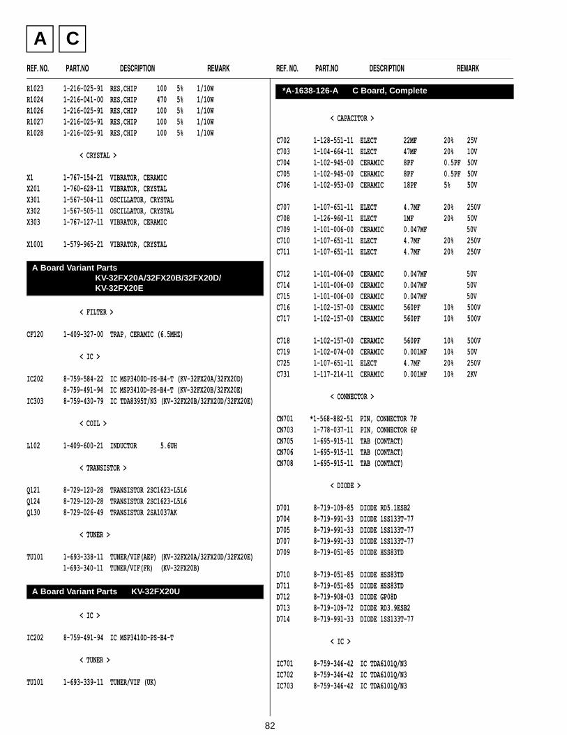
REF. NO. PART.NO DESCRIPTION REMARK REF. NO. PART.NO DESCRIPTION REMARK
The components identified byshading and marked are criticalfor safetyReplace only with the part numberspecified.
A C
R1023 1-216-025-91 RES,CHIP 100 5% 1/10WR1024 1-216-041-00 RES,CHIP 470 5% 1/10WR1026 1-216-025-91 RES,CHIP 100 5% 1/10WR1027 1-216-025-91 RES,CHIP 100 5% 1/10WR1028 1-216-025-91 RES,CHIP 100 5% 1/10W
< CRYSTAL >
X1 1-767-154-21 VIBRATOR, CERAMICX201 1-760-628-11 VIBRATOR, CRYSTALX301 1-567-504-11 OSCILLATOR, CRYSTALX302 1-567-505-11 OSCILLATOR, CRYSTALX303 1-767-127-11 VIBRATOR, CERAMIC
X1001 1-579-965-21 VIBRATOR, CRYSTAL
< FILTER >
CF120 1-409-327-00 TRAP, CERAMIC (6.5MHZ)
< IC >
IC202 8-759-584-22 IC MSP3400D-PS-B4-T (KV-32FX20A/32FX20D) 8-759-491-94 IC MSP3410D-PS-B4-T (KV-32FX20B/32FX20E)IC303 8-759-430-79 IC TDA8395T/N3 (KV-32FX20B/32FX20D/32FX20E)
< COIL >
L102 1-409-600-21 INDUCTOR 5.6UH
< TRANSISTOR >
Q121 8-729-120-28 TRANSISTOR 2SC1623-L5L6Q124 8-729-120-28 TRANSISTOR 2SC1623-L5L6Q130 8-729-026-49 TRANSISTOR 2SA1037AK
< TUNER >
TU101 1-693-338-11 TUNER/VIF(AEP) (KV-32FX20A/32FX20D/32FX20E) 1-693-340-11 TUNER/VIF(FR) (KV-32FX20B)
< IC >
IC202 8-759-491-94 IC MSP3410D-PS-B4-T
< TUNER >
TU101 1-693-339-11 TUNER/VIF (UK)
< CAPACITOR >
C702 1-128-551-11 ELECT 22MF 20% 25VC703 1-104-664-11 ELECT 47MF 20% 10VC704 1-102-945-00 CERAMIC 8PF 0.5PF 50VC705 1-102-945-00 CERAMIC 8PF 0.5PF 50VC706 1-102-953-00 CERAMIC 18PF 5% 50V
C707 1-107-651-11 ELECT 4.7MF 20% 250VC708 1-126-960-11 ELECT 1MF 20% 50VC709 1-101-006-00 CERAMIC 0.047MF 50VC710 1-107-651-11 ELECT 4.7MF 20% 250VC711 1-107-651-11 ELECT 4.7MF 20% 250V
C712 1-101-006-00 CERAMIC 0.047MF 50VC714 1-101-006-00 CERAMIC 0.047MF 50VC715 1-101-006-00 CERAMIC 0.047MF 50VC716 1-102-157-00 CERAMIC 560PF 10% 500VC717 1-102-157-00 CERAMIC 560PF 10% 500V
C718 1-102-157-00 CERAMIC 560PF 10% 500VC719 1-102-074-00 CERAMIC 0.001MF 10% 50VC725 1-107-651-11 ELECT 4.7MF 20% 250VC731 1-117-214-11 CERAMIC 0.001MF 10% 2KV
< CONNECTOR >
CN701 *1-568-882-51 PIN, CONNECTOR 7PCN703 1-778-037-11 PIN, CONNECTOR 6PCN705 1-695-915-11 TAB (CONTACT)CN706 1-695-915-11 TAB (CONTACT)CN708 1-695-915-11 TAB (CONTACT)
< DIODE >
D701 8-719-109-85 DIODE RD5.1ESB2D704 8-719-991-33 DIODE 1SS133T-77D705 8-719-991-33 DIODE 1SS133T-77D707 8-719-991-33 DIODE 1SS133T-77D709 8-719-051-85 DIODE HSS83TD
D710 8-719-051-85 DIODE HSS83TDD711 8-719-051-85 DIODE HSS83TDD712 8-719-908-03 DIODE GP08DD713 8-719-109-72 DIODE RD3.9ESB2D714 8-719-991-33 DIODE 1SS133T-77
< IC >
IC701 8-759-346-42 IC TDA6101Q/N3IC702 8-759-346-42 IC TDA6101Q/N3IC703 8-759-346-42 IC TDA6101Q/N3
A Board Variant PartsKV-32FX20A/32FX20B/32FX20D/KV-32FX20E
A Board Variant Parts KV-32FX20U
*A-1638-126-A C Board, Complete
82
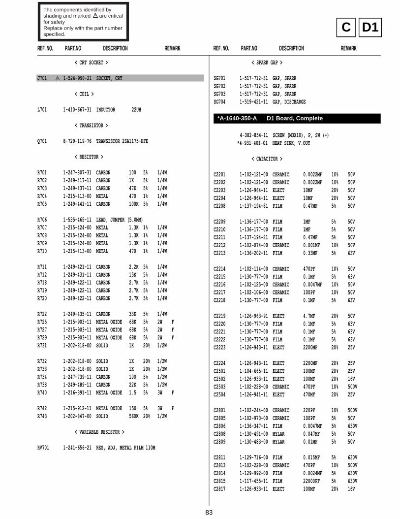
REF. NO. PART.NO DESCRIPTION REMARK REF. NO. PART.NO DESCRIPTION REMARK
The components identified byshading and marked are criticalfor safetyReplace only with the part numberspecified.
D1C
< CRT SOCKET >
J701 £ 1-526-990-21 SOCKET, CRT
< COIL >
L701 1-410-667-31 INDUCTOR 22UH
< TRANSISTOR >
Q701 8-729-119-76 TRANSISTOR 2SA1175-HFE
< RESISTOR >
R701 1-247-807-31 CARBON 100 5% 1/4WR702 1-249-417-11 CARBON 1K 5% 1/4WR703 1-249-437-11 CARBON 47K 5% 1/4WR704 1-215-413-00 METAL 470 1% 1/4WR705 1-249-441-11 CARBON 100K 5% 1/4W
R706 1-535-465-11 LEAD, JUMPER (5.0MM)R707 1-215-424-00 METAL 1.3K 1% 1/4WR708 1-215-424-00 METAL 1.3K 1% 1/4WR709 1-215-424-00 METAL 1.3K 1% 1/4WR710 1-215-413-00 METAL 470 1% 1/4W
R711 1-249-421-11 CARBON 2.2K 5% 1/4WR712 1-249-431-11 CARBON 15K 5% 1/4WR718 1-249-422-11 CARBON 2.7K 5% 1/4WR719 1-249-422-11 CARBON 2.7K 5% 1/4WR720 1-249-422-11 CARBON 2.7K 5% 1/4W
R722 1-249-435-11 CARBON 33K 5% 1/4WR725 1-215-903-11 METAL OXIDE 68K 5% 2W FR727 1-215-903-11 METAL OXIDE 68K 5% 2W FR729 1-215-903-11 METAL OXIDE 68K 5% 2W FR731 1-202-818-00 SOLID 1K 20% 1/2W
R732 1-202-818-00 SOLID 1K 20% 1/2WR733 1-202-818-00 SOLID 1K 20% 1/2WR734 1-247-739-11 CARBON 100 5% 1/2WR738 1-249-489-11 CARBON 22K 5% 1/2WR740 1-216-391-11 METAL OXIDE 1.5 5% 3W F
R742 1-215-912-11 METAL OXIDE 150 5% 3W FR743 1-202-847-00 SOLID 560K 20% 1/2W
< VARIABLE RESISTOR >
RV701 1-241-656-21 RES, ADJ, METAL FILM 110M
< SPARK GAP >
SG701 1-517-712-31 GAP, SPARKSG702 1-517-712-31 GAP, SPARKSG703 1-517-712-31 GAP, SPARKSG704 1-519-421-11 GAP, DISCHARGE
4-382-854-11 SCREW (M3X10), P, SW (+) *4-931-401-01 HEAT SINK, V.OUT
< CAPACITOR >
C2201 1-102-121-00 CERAMIC 0.0022MF 10% 50VC2202 1-102-121-00 CERAMIC 0.0022MF 10% 50VC2203 1-126-964-11 ELECT 10MF 20% 50VC2204 1-126-964-11 ELECT 10MF 20% 50VC2208 1-137-194-81 FILM 0.47MF 5% 50V
C2209 1-136-177-00 FILM 1MF 5% 50VC2210 1-136-177-00 FILM 1MF 5% 50VC2211 1-137-194-81 FILM 0.47MF 5% 50VC2212 1-102-074-00 CERAMIC 0.001MF 10% 50VC2213 1-136-202-11 FILM 0.33MF 5% 63V
C2214 1-102-114-00 CERAMIC 470PF 10% 50VC2215 1-130-777-00 FILM 0.1MF 5% 63VC2216 1-102-125-00 CERAMIC 0.0047MF 10% 50VC2217 1-102-106-00 CERAMIC 100PF 10% 50VC2218 1-130-777-00 FILM 0.1MF 5% 63V
C2219 1-126-963-91 ELECT 4.7MF 20% 50VC2220 1-130-777-00 FILM 0.1MF 5% 63VC2221 1-130-777-00 FILM 0.1MF 5% 63VC2222 1-130-777-00 FILM 0.1MF 5% 63VC2223 1-126-943-11 ELECT 2200MF 20% 25V
C2224 1-126-943-11 ELECT 2200MF 20% 25VC2501 1-104-665-11 ELECT 100MF 20% 25VC2502 1-126-933-11 ELECT 100MF 20% 16VC2503 1-102-228-00 CERAMIC 470PF 10% 500VC2504 1-126-941-11 ELECT 470MF 20% 25V
C2801 1-102-244-00 CERAMIC 220PF 10% 500VC2805 1-102-973-00 CERAMIC 100PF 5% 50VC2806 1-136-347-11 FILM 0.0047MF 5% 630VC2808 1-130-491-00 MYLAR 0.047MF 5% 50VC2809 1-130-483-00 MYLAR 0.01MF 5% 50V
C2811 1-129-716-00 FILM 0.015MF 5% 630VC2813 1-102-228-00 CERAMIC 470PF 10% 500VC2814 1-129-992-00 FILM 0.0024MF 5% 630VC2815 1-117-455-11 FILM 22000PF 5% 630VC2817 1-126-933-11 ELECT 100MF 20% 16V
*A-1640-350-A D1 Board, Complete
83
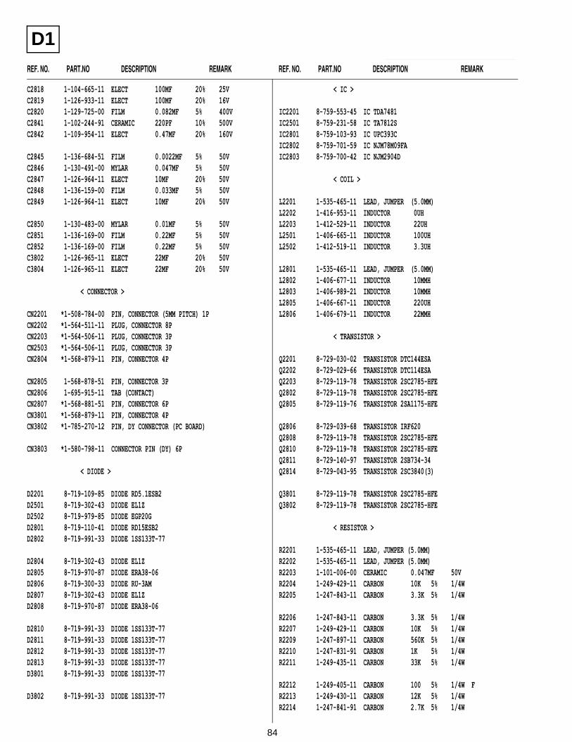
REF. NO. PART.NO DESCRIPTION REMARK REF. NO. PART.NO DESCRIPTION REMARK
The components identified byshading and marked are criticalfor safetyReplace only with the part numberspecified.
D1
C2818 1-104-665-11 ELECT 100MF 20% 25VC2819 1-126-933-11 ELECT 100MF 20% 16VC2820 1-129-725-00 FILM 0.082MF 5% 400VC2841 1-102-244-91 CERAMIC 220PF 10% 500VC2842 1-109-954-11 ELECT 0.47MF 20% 160V
C2845 1-136-684-51 FILM 0.0022MF 5% 50VC2846 1-130-491-00 MYLAR 0.047MF 5% 50VC2847 1-126-964-11 ELECT 10MF 20% 50VC2848 1-136-159-00 FILM 0.033MF 5% 50VC2849 1-126-964-11 ELECT 10MF 20% 50V
C2850 1-130-483-00 MYLAR 0.01MF 5% 50VC2851 1-136-169-00 FILM 0.22MF 5% 50VC2852 1-136-169-00 FILM 0.22MF 5% 50VC3802 1-126-965-11 ELECT 22MF 20% 50VC3804 1-126-965-11 ELECT 22MF 20% 50V
< CONNECTOR >
CN2201 *1-508-784-00 PIN, CONNECTOR (5MM PITCH) 1PCN2202 *1-564-511-11 PLUG, CONNECTOR 8PCN2203 *1-564-506-11 PLUG, CONNECTOR 3PCN2503 *1-564-506-11 PLUG, CONNECTOR 3PCN2804 *1-568-879-11 PIN, CONNECTOR 4P
CN2805 1-568-878-51 PIN, CONNECTOR 3PCN2806 1-695-915-11 TAB (CONTACT)CN2807 *1-568-881-51 PIN, CONNECTOR 6PCN3801 *1-568-879-11 PIN, CONNECTOR 4PCN3802 *1-785-270-12 PIN, DY CONNECTOR (PC BOARD)
CN3803 *1-580-798-11 CONNECTOR PIN (DY) 6P
< DIODE >
D2201 8-719-109-85 DIODE RD5.1ESB2D2501 8-719-302-43 DIODE EL1ZD2502 8-719-979-85 DIODE EGP20GD2801 8-719-110-41 DIODE RD15ESB2D2802 8-719-991-33 DIODE 1SS133T-77
D2804 8-719-302-43 DIODE EL1ZD2805 8-719-970-87 DIODE ERA38-06D2806 8-719-300-33 DIODE RU-3AMD2807 8-719-302-43 DIODE EL1ZD2808 8-719-970-87 DIODE ERA38-06
D2810 8-719-991-33 DIODE 1SS133T-77D2811 8-719-991-33 DIODE 1SS133T-77D2812 8-719-991-33 DIODE 1SS133T-77D2813 8-719-991-33 DIODE 1SS133T-77D3801 8-719-991-33 DIODE 1SS133T-77
D3802 8-719-991-33 DIODE 1SS133T-77
< IC >
IC2201 8-759-553-45 IC TDA7481IC2501 8-759-231-58 IC TA7812SIC2801 8-759-103-93 IC UPC393CIC2802 8-759-701-59 IC NJM78M09FAIC2803 8-759-700-42 IC NJM2904D
< COIL >
L2201 1-535-465-11 LEAD, JUMPER (5.0MM)L2202 1-416-953-11 INDUCTOR 0UHL2203 1-412-529-11 INDUCTOR 22UHL2501 1-406-665-11 INDUCTOR 100UHL2502 1-412-519-11 INDUCTOR 3.3UH
L2801 1-535-465-11 LEAD, JUMPER (5.0MM)L2802 1-406-677-11 INDUCTOR 10MMHL2803 1-406-989-21 INDUCTOR 10MMHL2805 1-406-667-11 INDUCTOR 220UHL2806 1-406-679-11 INDUCTOR 22MMH
< TRANSISTOR >
Q2201 8-729-030-02 TRANSISTOR DTC144ESAQ2202 8-729-029-66 TRANSISTOR DTC114ESAQ2203 8-729-119-78 TRANSISTOR 2SC2785-HFEQ2802 8-729-119-78 TRANSISTOR 2SC2785-HFEQ2805 8-729-119-76 TRANSISTOR 2SA1175-HFE
Q2806 8-729-039-68 TRANSISTOR IRF620Q2808 8-729-119-78 TRANSISTOR 2SC2785-HFEQ2810 8-729-119-78 TRANSISTOR 2SC2785-HFEQ2811 8-729-140-97 TRANSISTOR 2SB734-34Q2814 8-729-043-95 TRANSISTOR 2SC3840(3)
Q3801 8-729-119-78 TRANSISTOR 2SC2785-HFEQ3802 8-729-119-78 TRANSISTOR 2SC2785-HFE
< RESISTOR >
R2201 1-535-465-11 LEAD, JUMPER (5.0MM)R2202 1-535-465-11 LEAD, JUMPER (5.0MM)R2203 1-101-006-00 CERAMIC 0.047MF 50VR2204 1-249-429-11 CARBON 10K 5% 1/4WR2205 1-247-843-11 CARBON 3.3K 5% 1/4W
R2206 1-247-843-11 CARBON 3.3K 5% 1/4WR2207 1-249-429-11 CARBON 10K 5% 1/4WR2209 1-247-897-11 CARBON 560K 5% 1/4WR2210 1-247-831-91 CARBON 1K 5% 1/4WR2211 1-249-435-11 CARBON 33K 5% 1/4W
R2212 1-249-405-11 CARBON 100 5% 1/4W FR2213 1-249-430-11 CARBON 12K 5% 1/4WR2214 1-247-841-91 CARBON 2.7K 5% 1/4W
84
REF. NO. PART.NO DESCRIPTION REMARK REF. NO. PART.NO DESCRIPTION REMARK
The components identified byshading and marked are criticalfor safetyReplace only with the part numberspecified.
D2D1
R2215 1-247-841-91 CARBON 2.7K 5% 1/4WR2216 1-247-865-91 CARBON 27K 5% 1/4WR2501 1-249-443-11 CARBON 0.47 5% 1/4W FR2801 1-535-465-11 LEAD, JUMPER (5.0MM)R2802 1-215-919-11 METAL OXIDE 2.2K 5% 3W F
R2804 1-249-437-11 CARBON 47K 5% 1/4WR2805 1-249-429-11 CARBON 10K 5% 1/4WR2811 1-215-445-00 METAL 10K 1% 1/4WR2813 1-215-469-00 METAL 100K 1% 1/4WR2814 1-215-445-00 METAL 10K 1% 1/4W
R2815 1-215-469-00 METAL 100K 1% 1/4WR2816 1-215-443-00 METAL 8.2K 1% 1/4WR2817 1-215-463-00 METAL 56K 1% 1/4WR2818 1-215-459-00 METAL 39K 1% 1/4WR2819 1-249-421-11 CARBON 2.2K 5% 1/4W
R2820 1-249-421-11 CARBON 2.2K 5% 1/4WR2821 1-247-807-31 CARBON 100 5% 1/4WR2823 1-535-465-11 LEAD, JUMPER (5.0MM)R2824 1-249-425-11 CARBON 4.7K 5% 1/4WR2825 1-249-417-11 CARBON 1K 5% 1/4W
R2826 1-249-417-11 CARBON 1K 5% 1/4WR2827 1-249-441-11 CARBON 100K 5% 1/4WR2828 1-249-441-11 CARBON 100K 5% 1/4WR2829 1-249-441-11 CARBON 100K 5% 1/4WR2830 1-215-912-11 METAL OXIDE 150 5% 3W F
R2831 1-215-912-11 METAL OXIDE 150 5% 3W FR2832 1-249-379-11 CARBON 0.68 5% 1/4W FR2840 1-215-922-11 METAL OXIDE 6.8K 5% 3W FR2841 1-215-922-11 METAL OXIDE 6.8K 5% 3W FR2842 1-215-921-21 METAL OXIDE 4.7K 5% 3W F
R2843 1-215-921-21 METAL OXIDE 4.7K 5% 3W FR2844 1-249-409-11 CARBON 220 5% 1/4W FR2845 1-215-489-00 METAL 680K 1% 1/4WR2846 1-247-903-00 CARBON 1M 5% 1/4WR2847 1-249-429-11 CARBON 10K 5% 1/4W
R2848 1-215-449-00 METAL 15K 1% 1/4WR2849 1-215-491-00 METAL 820K 1% 1/4WR2850 1-215-445-00 METAL 10K 1% 1/4WR2851 1-215-445-00 METAL 10K 1% 1/4WR2852 1-215-481-00 METAL 330K 1% 1/4W
R2853 1-215-477-00 METAL 220K 1% 1/4WR2854 1-215-457-00 METAL 33K 1% 1/4WR2855 1-215-457-00 METAL 33K 1% 1/4WR2856 1-247-807-31 CARBON 100 5% 1/4WR2857 1-249-413-11 CARBON 470 5% 1/4W
R2858 1-249-424-11 CARBON 3.9K 5% 1/4WR2859 1-247-807-31 CARBON 100 5% 1/4W
R2860 1-215-886-11 METAL OXIDE 100 5% 2W FR2861 1-215-886-11 METAL OXIDE 100 5% 2W FR3801 1-249-421-11 CARBON 2.2K 5% 1/4WR3804 1-249-421-11 CARBON 2.2K 5% 1/4W
< RELAY >
RY3801 1-755-172-11 RELAYRY3802 1-755-172-11 RELAY
< TRANSFORMER >
T2801 1-433-849-11 TRANSFORMER, FERRITE (DFT)T3801 1-419-090-11 COIL, CHOKE (100UH)T3802 1-419-090-11 COIL, CHOKE (100UH)
4-382-854-11 SCREW (M3X10), P, SW (+)
< CAPACITOR >
C8801 1-107-683-11 ELECT 2.2MF 0 250VC8804 1-136-207-11 FILM 0.047MF 10% 250VC8805 1-136-105-11 FILM 0.33MF 5% 200V
< CONNECTOR >
CN8801 *1-770-748-11 CONNECTOR, BOARD TO BOARD 12P
< DIODE >
D8801 8-719-923-60 DIODE MTZJ-T-77-9.1AD8802 8-719-302-43 DIODE EL1Z
< IC >
IC8801 8-749-010-64 PHOTO COUPLER PC123F2
< COIL >
L8801 1-406-674-11 INDUCTOR 3.3MMHL8802 1-406-978-11 INDUCTOR 150UH
< TRANSISTOR >
Q8802 8-729-030-02 TRANSISTOR DTC144ESAQ8803 8-729-030-02 TRANSISTOR DTC144ESA
< RESISTOR >
R8801 1-215-909-11 METAL OXIDE 47 5% 3W FR8802 1-249-441-11 CARBON 100K 5% 1/4WR8803 1-249-441-11 CARBON 100K 5% 1/4WR8804 1-249-421-11 CARBON 2.2K 5% 1/4WR8805 1-249-429-11 CARBON 10K 5% 1/4W
*A-1642-251-A D2 Board, Complete
85
REF. NO. PART.NO DESCRIPTION REMARK REF. NO. PART.NO DESCRIPTION REMARK
The components identified byshading and marked are criticalfor safetyReplace only with the part numberspecified.
DD2
R8806 1-247-807-31 CARBON 100 5% 1/4WR8807 1-202-885-91 RES, SOLID 1M 20% 1/2W
4-201-023-01 SPACER, INSULATING 4-202-373-01 SPRING, IC 4-202-710-01 SPACER, INSULATING 4-382-854-11 SCREW (M3X10), P, SW (+)
< CAPACITOR >
C502 1-102-119-00 CERAMIC 0.0015MF 10% 50VC503 1-136-165-00 FILM 0.1MF 5% 50VC504 1-102-119-00 CERAMIC 0.0015MF 10% 50VC506 1-126-941-11 ELECT 470MF 20% 25VC507 1-109-953-11 ELECT 2.2MF 20% 50V
C509 1-136-165-00 FILM 0.1MF 5% 50VC510 1-126-969-11 ELECT 220MF 20% 50VC511 1-136-202-11 FILM 0.33MF 5% 63VC513 1-106-220-00 MYLAR 0.1MF 10% 100VC514 1-136-165-00 FILM 0.1MF 5% 50V
C515 1-126-941-11 ELECT 470MF 20% 25VC517 1-126-941-11 ELECT 470MF 20% 25VC518 1-102-228-00 CERAMIC 470PF 10% 500VC519 1-102-228-00 CERAMIC 470PF 10% 500VC520 1-126-941-11 ELECT 470MF 20% 25V
C521 1-107-698-11 ELECT 10MF 20% 25VC522 1-126-964-11 ELECT 10MF 20% 50VC523 1-136-165-00 FILM 0.1MF 5% 50VC600 £ 1-119-888-51 CERAMIC 0.0022MF 20% 250VC601 £ 1-161-964-91 CERAMIC 0.0047MF 250V
C602 £ 1-161-964-91 CERAMIC 0.0047MF 250VC603 1-117-752-11 ELECT(BLOCK) 330MF 20% 450VC604 1-126-968-11 ELECT 100MF 20% 50VC605 1-107-929-11 ELECT 10MF 20% 100VC606 1-162-318-11 CERAMIC 0.001MF 10% 500V
C607 1-104-666-11 ELECT 220MF 20% 25VC608 1-109-880-11 FILM 0.0015MF 3% 2KVC611 1-102-228-00 CERAMIC 470PF 10% 500VC613 1-124-347-00 ELECT 100MF 20% 160VC614 1-126-933-11 ELECT 100MF 20% 16V
C615 1-115-789-11 ELECT 0.001F 20% 25VC616 1-115-789-11 ELECT 0.001F 20% 25VC618 1-136-165-00 FILM 0.1MF 5% 50VC619 1-102-228-00 CERAMIC 470PF 10% 500VC620 1-102-228-00 CERAMIC 470PF 10% 500V
C622 1-107-925-11 ELECT 1MF 20% 100VC624 1-136-165-00 FILM 0.1MF 5% 50V
C625 1-126-967-11 ELECT 47MF 20% 50VC626 1-104-666-11 ELECT 220MF 20% 25VC628 1-126-964-11 ELECT 10MF 20% 50VC629 1-115-819-11 ELECT 0.0022F 20% 35VC630 1-115-819-11 ELECT 0.0022F 20% 35V
C631 1-126-965-11 ELECT 22MF 20% 50VC632 1-104-666-11 ELECT 220MF 20% 25VC636 £ 1-119-888-51 CERAMIC 0.0022MF 20% 250VC638 1-136-203-11 FILM 0.01MF 10% 250VC640 1-106-220-00 MYLAR 0.1MF 10% 100V
C641 £ 1-113-916-11 CERAMIC 0.01MF 20% 250VC642 £ 1-113-916-11 CERAMIC 0.01MF 20% 250VC647 1-162-116-00 CERAMIC 680PF 10% 2KVC651 1-102-228-00 CERAMIC 470PF 10% 500VC800 1-137-368-11 FILM 0.0047MF 5% 50V
C801 1-137-372-11 FILM 0.022MF 5% 50VC802 1-102-117-91 CERAMIC 820PF 10% 50VC803 1-129-898-00 FILM 0.0022MF 5% 630VC804 1-136-165-00 FILM 0.1MF 5% 50VC805 1-136-207-11 FILM 0.047MF 10% 250V
C806 1-107-370-11 FILM 0.1MF 10% 200VC807 1-136-540-11 FILM 0.82MF 5% 200VC811 1-162-318-11 CERAMIC 0.001MF 10% 500VC812 1-136-540-11 FILM 0.82MF 5% 200VC813 1-129-724-00 FILM 0.068MF 5% 630V
C814 1-136-952-11 FILM 0.02MF 3% 1.4KVC815 1-137-046-11 FILM 0.0082MF 10% 400VC816 1-117-214-11 CERAMIC 0.001MF 10% 2KVC817 1-117-214-11 CERAMIC 0.001MF 10% 2KVC818 1-117-214-11 CERAMIC 0.001MF 10% 2KV
C819 1-136-208-11 FILM 0.068MF 10% 250VC822 1-107-662-11 ELECT 22MF 20% 250VC824 1-123-024-21 ELECT 33MF 160VC826 1-161-830-00 CERAMIC 0.0047MF 500VC829 1-126-959-11 ELECT 0.47MF 20% 50V
C832 1-126-960-91 ELECT 1MF 20% 25VC834 1-128-551-11 ELECT 22MF 20% 25VC835 1-162-318-11 CERAMIC 0.001MF 10% 500VC836 1-162-117-00 CERAMIC 100PF 10% 500VC838 1-102-228-00 CERAMIC 470PF 10% 500V
C839 1-136-207-11 FILM 0.047MF 10% 250VC841 1-102-114-00 CERAMIC 470PF 10% 50VC845 1-101-880-00 CERAMIC 47PF 5% 50VC910 1-535-465-11 LEAD,JUMPER (5.0MM)C916 1-162-318-11 CERAMIC 0.001MF 10% 500V
C1200 1-136-165-00 FILM 0.1MF 5% 50VC1201 1-137-194-81 FILM 0.47MF 5% 50V
*A-1642-252-A D Board, Complete
86
REF. NO. PART.NO DESCRIPTION REMARK REF. NO. PART.NO DESCRIPTION REMARK
The components identified byshading and marked are criticalfor safetyReplace only with the part numberspecified.
D
C1202 1-137-194-81 FILM 0.47MF 5% 50VC1203 1-136-169-00 FILM 0.22MF 5% 50VC1204 1-136-169-00 FILM 0.22MF 5% 50VC1205 1-101-005-00 CERAMIC 0.022MF 50VC1206 1-101-005-00 CERAMIC 0.022MF 50V
C1207 1-126-933-11 ELECT 100MF 20% 16VC1208 1-126-963-11 ELECT 4.7MF 20% 50VC1209 1-126-963-11 ELECT 4.7MF 20% 50VC1210 1-126-941-11 ELECT 470MF 20% 25VC1212 1-162-318-11 CERAMIC 0.001MF 10% 500V
C1213 1-162-318-11 CERAMIC 0.001MF 10% 500VC1214 1-126-933-11 ELECT 100MF 20% 16VC1215 1-137-194-81 FILM 0.47MF 5% 50VC1216 1-137-366-11 FILM 0.0022MF 5% 50VC1217 1-137-366-11 FILM 0.0022MF 5% 50V
C1218 1-126-941-11 ELECT 470MF 20% 25VC1220 1-162-318-11 CERAMIC 0.001MF 10% 500VC1221 1-162-318-11 CERAMIC 0.001MF 10% 500VC1223 1-101-006-00 CERAMIC 0.047MF 50V
< CONNECTOR >
CN600 £ *1-508-786-00 PIN, CONNECTOR (5MM PITCH) 2PCN601 £ 1-508-765-00 PIN, CONNECTOR (5MM PITCH) 3PCN602 £ *1-691-291-11 PIN, CONNECTOR (PC BOARD) 5PCN613 4-352-844-01 PIN, LEAD, COATINGCN614 1-695-915-11 TAB (CONTACT)
CN615 1-695-915-11 TAB (CONTACT)CN616 4-352-844-01 PIN, LEAD, COATINGCN800 *1-580-798-11 CONNECTOR PIN (DY) 6PCN801 *1-568-879-11 PIN, CONNECTOR 4PCN802 1-695-915-11 TAB (CONTACT)
CN803 1-695-915-11 TAB (CONTACT)CN804 1-778-037-11 PIN, CONNECTOR 6PCN805 *1-770-747-11 CONNECTOR, BOARD TO BOARD 12PCN901 *1-568-882-51 PIN, CONNECTOR 7PCN902 1-695-299-11 CONNECTOR, BOARD TO BOARD 50P
CN903 *1-564-516-11 PLUG, CONNECTOR 13PCN904 *1-564-511-11 PLUG, CONNECTOR 8PCN1401 *1-568-880-51 PIN, CONNECTOR 5PCN1403 *1-564-511-11 PLUG, CONNECTOR 8PCN1408 *1-568-879-11 PIN, CONNECTOR 4P
CN1803 *1-564-508-11 PLUG, CONNECTOR 5P
< DIODE >
D500 8-719-109-85 DIODE RD5.1ESB2D502 8-719-979-85 DIODE EGP20GD503 8-719-979-85 DIODE EGP20G
D504 8-719-991-33 DIODE 1SS133T-77D505 8-719-982-03 DIODE MTZJ-3.6AD506 8-719-991-33 DIODE 1SS133T-77D507 8-719-109-85 DIODE RD5.1ESB2D510 8-719-924-13 DIODE MTZJ-T-77-22B
D570 8-719-924-13 DIODE MTZJ-T-77-22BD571 8-719-924-13 DIODE MTZJ-T-77-22BD600 8-719-510-53 DIODE D4SB60LD601 8-719-046-77 DIODE EM1-V1D603 8-719-109-97 DIODE RD6.8ESB2
D604 8-719-046-75 DIODE EU-1-V1D605 8-719-302-43 DIODE EL1ZD606 8-719-302-43 DIODE EL1ZD607 8-719-046-78 DIODE EG-1Z-V1D608 8-719-302-06 DIODE EU2A
D609 8-719-053-32 DIODE FMU-G16SD611 8-719-058-38 DIODE FMN-G12SD612 8-719-058-38 DIODE FMN-G12SD613 8-719-058-38 DIODE FMN-G12SD614 8-719-058-38 DIODE FMN-G12S
D617 8-719-991-33 DIODE 1SS133T-77D618 8-719-991-33 DIODE 1SS133T-77D619 8-719-991-33 DIODE 1SS133T-77D620 8-719-991-33 DIODE 1SS133T-77D622 8-719-923-60 DIODE MTZJ-T-77-9.1A
D625 8-719-991-33 DIODE 1SS133T-77D637 8-719-110-17 DIODE RD10ESB2D638 8-719-991-33 DIODE 1SS133T-77D800 8-719-991-33 DIODE 1SS133T-77D801 8-719-991-33 DIODE 1SS133T-77
D802 1-535-465-11 LEAD, JUMPER (5.0MM)D803 8-719-908-03 DIODE GP08DD807 8-719-302-43 DIODE EL1ZD808 8-719-908-03 DIODE GP08DD810 8-719-302-43 DIODE EL1Z
D811 8-719-110-41 DIODE RD15ESB2D812 8-719-038-49 DIODE FMS-3FU-LF027-103D815 8-719-908-03 DIODE GP08DD817 8-719-109-85 DIODE RD5.1ESB2D902 8-719-923-60 DIODE MTZJ-T-77-9.1A
D903 8-719-923-60 DIODE MTZJ-T-77-9.1AD904 8-719-923-60 DIODE MTZJ-T-77-9.1AD905 8-719-923-60 DIODE MTZJ-T-77-9.1AD906 8-719-923-60 DIODE MTZJ-T-77-9.1AD920 8-719-109-89 DIODE RD5.6ESB2
D1201 8-719-109-72 DIODE RD3.9ESB2
87
REF. NO. PART.NO DESCRIPTION REMARK REF. NO. PART.NO DESCRIPTION REMARK
The components identified byshading and marked are criticalfor safetyReplace only with the part numberspecified.
D
< FERRITE BEAD >
FB501 1-410-397-21 FERRITE 1.1UHFB600 1-410-396-41 FERRITE 0.45UHFB601 1-410-396-41 FERRITE 0.45UHFB602 1-410-397-21 FERRITE 1.1UHFB603 1-410-396-41 FERRITE 0.45UH
FB604 1-410-396-41 FERRITE 0.45UHFB605 1-410-396-41 FERRITE 0.45UHFB606 1-410-397-21 FERRITE 1.1UHFB607 1-410-397-21 FERRITE 1.1UHFB608 1-410-396-41 FERRITE 0.45UH
FB800 1-410-397-21 FERRITE 1.1UHFB801 1-410-396-41 FERRITE 0.45UHFB901 1-535-465-41 LEAD, JUMPER (5.0MM)FB902 1-535-465-41 LEAD, JUMPER (5.0MM)
< ENCAPSULATED FILTER >
FL501 1-236-163-41 ENCAPSULATED COMPONENT
< IC >
IC500 8-759-192-71 IC STV9379IC600 8-749-010-92 IC STR-S6709IC601 £ 8-749-013-21 IC TLP721(D4-G)IC602 8-749-016-19 IC SE135N-LF4IC603 8-759-144-82 IC UPC2405HF
IC606 8-759-267-25 IC LM2940T-9.0IC800 8-759-103-93 IC UPC393CIC1200 8-759-585-29 IC TDA7264AIC1201 8-759-502-21 IC TDA2822M
< SOCKET >
J1200 1-770-218-11 JACK, PIN
< COIL >
L501 1-535-465-11 LEAD, JUMPER (5.0MM)L502 1-412-519-11 INDUCTOR 3.3UHL503 1-412-519-11 INDUCTOR 3.3UHL609 1-412-533-21 INDUCTOR 47UHL610 1-535-465-11 LEAD, JUMPER (5.0MM)
L611 1-412-527-11 INDUCTOR 15UHL612 1-412-522-41 INDUCTOR 5.6UHL613 1-412-522-41 INDUCTOR 5.6UHL615 1-412-529-11 INDUCTOR 22UHL616 1-412-533-21 INDUCTOR 47UH
L801 1-459-111-00 INDUCTOR 10MMHL802 1-459-104-00 COIL, WITH CORE
L803 1-535-465-11 LEAD, JUMPER (5.0MM)L806 1-535-465-11 LEAD, JUMPER (5.0MM)L809 1-408-611-31 INDUCTOR 47UHL813 1-412-552-11 INDUCTOR 2.2MMH
< IC LINK >
PS600 £ 1-532-686-21 LINK, IC 2.7A (ICP-F75)PS601 £ 1-532-686-21 LINK, IC 2.7A (ICP-F75)PS602 £ 1-532-686-21 LINK, IC 2.7A (ICP-F75)PS603 £ 1-532-686-21 LINK, IC 2.7A (ICP-F75)
< TRANSISTOR >
Q501 8-729-119-78 TRANSISTOR 2SC2785-HFEQ502 8-729-119-76 TRANSISTOR 2SA1175-HFEQ503 8-729-030-02 TRANSISTOR DTC144ESAQ601 8-729-025-04 TRANSISTOR 2SC3852AQ605 8-729-119-78 TRANSISTOR 2SC2785-HFE
Q606 8-729-029-56 TRANSISTOR DTA144ESAQ607 8-729-119-78 TRANSISTOR 2SC2785-HFEQ611 8-729-200-21 TRANSISTOR 2SC2500-BQ801 8-729-039-68 TRANSISTOR IRF620Q802 8-729-042-86 TRANSISTOR 2SC5251-01
Q803 8-729-119-80 TRANSISTOR 2SC2688-LKQ805 8-729-030-02 TRANSISTOR DTC144ESAQ900 8-729-119-78 TRANSISTOR 2SC2785-HFEQ1200 8-729-119-78 TRANSISTOR 2SC2785-HFEQ1201 8-729-029-94 TRANSISTOR DTC143TSA
Q1202 8-729-029-66 TRANSISTOR DTC114ESAQ1203 8-729-029-94 TRANSISTOR DTC143TSAQ1204 8-729-029-94 TRANSISTOR DTC143TSA
< RESISTOR >
JW010 1-410-397-21 FERRITE 1.1UHJW125 1-247-841-91 CARBON 2.7K 5% 1/4W
R500 1-215-457-00 METAL 33K 1% 1/4WR502 1-249-421-11 CARBON 2.2K 5% 1/4WR503 1-249-429-11 CARBON 10K 5% 1/4WR504 1-215-447-00 METAL 12K 1% 1/4WR505 1-249-382-11 CARBON 1.2 5% 1/4W F
R506 1-215-455-00 METAL 27K 1% 1/4WR507 1-215-888-00 METAL OXIDE 220 5% 2W FR508 1-216-371-00 METAL OXIDE 1.5 5% 2W FR509 1-249-443-11 CARBON 0.47 5% 1/4W FR510 1-249-443-11 CARBON 0.47 5% 1/4W F
R519 1-215-451-00 METAL 18K 1% 1/4WR520 1-215-451-00 METAL 18K 1% 1/4WR521 1-215-459-00 METAL 39K 1% 1/4W
88
REF. NO. PART.NO DESCRIPTION REMARK REF. NO. PART.NO DESCRIPTION REMARK
The components identified byshading and marked are criticalfor safetyReplace only with the part numberspecified.
D
R522 1-247-863-91 CARBON 22K 5% 1/4WR523 1-247-863-91 CARBON 22K 5% 1/4WR524 1-249-425-11 CARBON 4.7K 5% 1/4WR525 1-249-425-11 CARBON 4.7K 5% 1/4WR526 1-249-421-11 CARBON 2.2K 5% 1/4W
R527 1-215-433-00 METAL 3.3K 1% 1/4WR540 1-249-441-11 CARBON 100K 5% 1/4WR600 £ 1-216-490-11 METAL OXIDE 39K 5% 3W FR601 1-249-417-11 CARBON 1K 5% 1/4WR602 1-215-473-00 METAL 150K 1% 1/4W
R603 1-215-898-11 METAL OXIDE 10K 5% 2W FR604 1-249-420-11 CARBON 1.8K 5% 1/4WR605 1-216-362-11 METAL OXIDE 0.27 5% 2W FR606 1-535-143-21 LEAD, JUMPER (12.5MM)R607 1-216-421-11 METAL OXIDE 12 5% 1W F
R608 1-216-365-00 METAL OXIDE 0.47 5% 2W FR609 1-535-465-11 LEAD, JUMPER (5.0MM)R610 1-215-427-00 METAL 1.8K 1% 1/4WR612 1-249-428-11 CARBON 8.2K 5% 1/4WR616 1-215-471-00 METAL 120K 1% 1/4W
R617 1-215-901-00 METAL OXIDE 33K 5% 2W FR618 1-247-863-91 CARBON 22K 5% 1/4WR619 1-216-425-11 METAL OXIDE 56 5% 1W FR620 1-260-131-11 CARBON 470K 5% 1/2WR621 1-216-425-11 METAL OXIDE 56 5% 1W F
R622 1-249-437-11 CARBON 47K 5% 1/4WR623 1-249-429-11 CARBON 10K 5% 1/4WR624 1-249-393-11 CARBON 10 5% 1/4W FR625 1-249-434-11 CARBON 27K 5% 1/4WR626 1-249-430-11 CARBON 12K 5% 1/4W
R627 1-216-347-11 METAL OXIDE 0.68 5% 1W FR628 1-249-415-11 CARBON 680 5% 1/4W FR631 £ 1-202-968-11 CEMENTED 1.2 5% 10WR632 1-247-807-31 CARBON 100 5% 1/4WR633 1-247-807-31 CARBON 100 5% 1/4W
R634 1-249-397-11 CARBON 22 5% 1/4W FR636 1-249-417-11 CARBON 1K 5% 1/4WR637 1-247-815-91 CARBON 220 5% 1/4WR638 1-247-863-91 CARBON 22K 5% 1/4WR639 1-215-425-00 METAL 1.5K 1% 1/4W
R641 £ 1-240-030-91 METAL 4.7M 5% 1/2WR642 £ 1-202-968-11 CEMENTED 1.2 5% 10WR643 £ 1-240-030-91 METAL 4.7M 5% 1/2WR646 1-249-377-11 CARBON 0.47 5% 1/4W FR647 1-202-933-61 FUSIBLE 0.1 10% 1/2W F
R648 £ 1-202-968-11 CEMENTED 1.2 5% 10WR649 1-249-426-11 CARBON 5.6K 5% 1/4W
R650 1-249-429-11 CARBON 10K 5% 1/4WR800 1-249-429-11 CARBON 10K 5% 1/4WR802 1-215-453-00 METAL 22K 1% 1/4WR803 1-249-427-11 CARBON 6.8K 5% 1/4WR805 1-249-435-11 CARBON 33K 5% 1/4W
R808 1-215-888-00 METAL OXIDE 220 5% 2W FR809 1-247-897-11 CARBON 560K 5% 1/4WR810 1-215-888-00 METAL OXIDE 220 5% 2W FR812 1-249-421-11 CARBON 2.2K 5% 1/4WR813 1-249-417-11 CARBON 1K 5% 1/4W F
R814 1-249-381-11 CARBON 1 5% 1/4W FR815 1-249-381-11 CARBON 1 5% 1/4W FR816 1-215-917-11 METAL OXIDE 1K 5% 3W FR818 1-215-884-11 METAL OXIDE 47 5% 2W FR819 1-535-143-71 LEAD, JUMPER (7.5MM)
R820 1-249-403-11 CARBON 68 5% 1/4WR822 1-215-868-00 METAL OXIDE 680 5% 1W FR823 1-215-918-00 METAL OXIDE 1.5K 5% 3W FR824 1-249-420-11 CARBON 1.8K 5% 1/4WR825 1-215-884-11 METAL OXIDE 47 5% 2W F
R826 1-260-099-11 CARBON 1K 5% 1/2WR827 1-249-425-11 CARBON 4.7K 5% 1/4WR828 1-249-432-11 CARBON 18K 5% 1/4WR829 1-260-120-11 CARBON 56K 5% 1/2WR831 1-535-465-11 LEAD, JUMPER (5.0MM)
R833 1-247-887-00 CARBON 220K 5% 1/4WR835 1-215-907-11 METAL OXIDE 22 5% 3W FR836 1-249-439-11 CARBON 68K 5% 1/4WR838 1-215-455-00 METAL 27K 1% 1/4WR840 1-247-807-31 CARBON 100 5% 1/4W
R841 1-249-418-11 CARBON 1.2K 5% 1/4WR842 1-249-441-11 CARBON 100K 5% 1/4WR844 1-535-143-11 LEAD, JUMPER (10.0MM)R846 1-259-883-11 CARBON 3.9M 5% 1/4WR847 1-259-880-11 CARBON 2.2M 5% 1/4W
R848 1-259-880-11 CARBON 2.2M 5% 1/4WR849 1-249-429-11 CARBON 10K 5% 1/4WR851 1-215-898-11 METAL OXIDE 10K 5% 2W FR852 1-249-432-11 CARBON 18K 5% 1/4WR853 1-216-361-00 METAL OXIDE 0.22 5% 2W F
R901 1-260-082-11 CARBON 39 5% 1/2WR902 1-260-082-11 CARBON 39 5% 1/2WR909 1-249-429-11 CARBON 10K 5% 1/4WR922 1-247-807-31 CARBON 100 5% 1/4WR923 1-249-416-11 CARBON 820 5% 1/4W
R1200 1-249-425-11 CARBON 4.7K 5% 1/4WR1201 1-249-434-11 CARBON 27K 5% 1/4W
89
REF. NO. PART.NO DESCRIPTION REMARK REF. NO. PART.NO DESCRIPTION REMARK
The components identified byshading and marked are criticalfor safetyReplace only with the part numberspecified.
VMD
R1202 1-249-389-11 CARBON 4.7 5% 1/4W FR1203 1-249-417-11 CARBON 1K 5% 1/4WR1204 1-249-417-11 CARBON 1K 5% 1/4WR1205 1-249-428-11 CARBON 8.2K 5% 1/4WR1206 1-249-428-11 CARBON 8.2K 5% 1/4W
R1207 1-249-413-11 CARBON 470 5% 1/4WR1208 1-212-849-00 FUSIBLE 4.7 5% 1/4W FR1209 1-212-849-00 FUSIBLE 4.7 5% 1/4W FR1210 1-249-413-11 CARBON 470 5% 1/4WR1211 1-249-424-11 CARBON 3.9K 5% 1/4W
R1212 1-249-424-11 CARBON 3.9K 5% 1/4WR1213 1-249-421-11 CARBON 2.2K 5% 1/4WR1216 1-249-413-11 CARBON 470 5% 1/4WR1217 1-249-425-11 CARBON 4.7K 5% 1/4WR1218 1-535-465-11 LEAD, JUMPER (5.0MM)
R1219 1-249-417-11 CARBON 1K 5% 1/4WR1220 1-247-863-91 CARBON 22K 5% 1/4WR1221 1-247-863-91 CARBON 22K 5% 1/4W
< RELAY >
RY600 £ 1-755-018-11 RELAYRY601 £ 1-755-266-11 RELAY, AC POWER
< SWITCH >
S801 1-572-707-11 SWITCH, LEVER
< SPARK GAP >
SG801 1-519-422-11 GAP, SPARKSG802 1-519-422-11 GAP, SPARKSG803 1-519-422-11 GAP, SPARK
< TRANSFORMER >
T601 £ 1-429-604-11 TRANSFORMER, CONVERTERT800 1-426-981-11 TRANSFORMER, FERRITE (PMT)T803 £ X-4560-158-1 TRANSFORMER ASSY, FLYBACK (NX-4404//U2B4)T804 1-437-195-14 TRANSFORMER, HORIZONTAL DRIVET805 1-435-107-11 TRANSFORMER, HORIZONTAL LINEAR
< THERMISTOR >
THP600 £ 1-809-827-11 THERMISTOR, POSITIVE
4-382-854-11 SCREW (M3X10), P, SW (+)
< CAPACITOR >
C1501 1-104-664-11 ELECT 47MF 20% 16V
C1502 1-130-777-00 FILM 0.1MF 5% 63VC1503 1-102-510-11 CERAMIC 12PF 5% 50VC1504 1-136-177-00 FILM 1MF 5% 50VC1505 1-136-177-00 FILM 1MF 5% 50VC1506 1-102-973-00 CERAMIC 100PF 5% 50V
C1507 1-130-777-00 FILM 0.1MF 5% 63VC1508 1-104-664-11 ELECT 47MF 20% 16VC1509 1-136-202-11 FILM 0.33MF 5% 63VC1510 1-102-980-00 CERAMIC 270PF 5% 50VC1511 1-130-777-00 FILM 0.1MF 5% 63V
C1512 1-130-777-00 FILM 0.1MF 5% 63VC1513 1-126-964-11 ELECT 10MF 20% 50VC1514 1-126-967-11 ELECT 47MF 20% 50VC1515 1-126-967-11 ELECT 47MF 20% 50VC1516 1-102-852-91 CERAMIC 47PF 5% 50V
C1701 1-126-933-11 ELECT 100MF 20% 16VC1702 1-126-933-11 ELECT 100MF 20% 16VC1703 1-130-491-00 MYLAR 0.047MF 5% 50VC1704 1-107-648-91 ELECT 100MF 20% 160VC1705 1-107-638-11 ELECT 33MF 20% 160V
C1706 1-104-999-11 FILM 0.1MF 5% 200VC1707 1-137-397-11 FILM 0.047MF 5% 100VC1708 1-130-471-00 FILM 0.001MF 5% 50VC1709 1-130-471-00 FILM 0.001MF 5% 50VC1710 1-102-959-91 CERAMIC 22PF 5% 50V
C1711 1-126-962-11 ELECT 3.3MF 20% 50VC1720 1-107-667-11 ELECT 2.2MF 20% 160VC1721 1-137-397-11 FILM 0.047MF 5% 100VC1722 1-126-935-11 ELECT 470MF 20% 16VC1723 1-161-830-00 CERAMIC 0.0047MF 500V
C1725 1-128-551-11 ELECT 22MF 20% 25VC1726 1-136-153-00 FILM 0.01MF 5% 50VC1801 1-104-664-11 ELECT 47MF 20% 25VC1803 1-137-368-11 FILM 0.0047MF 5% 50VC1804 1-126-964-11 ELECT 10MF 20% 50V
C1805 1-137-366-11 FILM 0.0022MF 5% 50V
< CONNECTOR >
CN1501 *1-564-506-11 PLUG, CONNECTOR 3PCN1502 *1-564-508-11 PLUG, CONNECTOR 5PCN1503 *1-564-506-11 PLUG, CONNECTOR 3PCN1716 *1-568-880-51 PIN, CONNECTOR 5PCN1717 *1-568-881-51 PIN, CONNECTOR 6P
CN1718 *1-770-723-11 CONNECTOR, BOARD TO BOARD 8PCN1719 1-568-878-51 PIN, CONNECTOR 3PCN1801 *1-564-508-11 PLUG, CONNECTOR 5PCN1802 *1-568-878-51 PIN, CONNECTOR 3P
*A-1644-098-A VM Board, Complete
90
REF. NO. PART.NO DESCRIPTION REMARK REF. NO. PART.NO DESCRIPTION REMARK
The components identified byshading and marked are criticalfor safetyReplace only with the part numberspecified.
VM
< DIODE >
D1501 8-719-991-33 DIODE 1SS133T-77D1502 8-719-991-33 DIODE 1SS133T-77D1503 8-719-991-33 DIODE 1SS133T-77D1504 8-719-991-33 DIODE 1SS133T-77D1505 1-535-465-11 LEAD, JUMPER (5.0MM)
D1506 8-719-911-19 DIODE 1SS119-25D1701 8-719-991-33 DIODE 1SS133T-77D1702 8-719-110-88 DIODE RD39ESB2D1703 8-719-110-88 DIODE RD39ESB2D1801 8-719-929-15 DIODE HZS9.1NB2
< IC >
IC1501 8-759-478-66 IC CXA8070PIC1502 8-759-903-16 IC LM318PIC1801 8-759-701-59 IC NJM78M09FAIC1802 8-759-603-37 IC M5216P
< COIL >
L1701 1-535-465-11 LEAD, JUMPER (5.0MM)L1703 1-408-603-31 INDUCTOR 10UHL1704 1-408-603-31 INDUCTOR 10UH
< IC LINK >
PS1801 £ 1-532-605-00 LINK, IC 0.4A (ICPN10)
< TRANSISTOR >
Q1501 8-729-119-78 TRANSISTOR 2SC2785-HFEQ1502 8-729-119-78 TRANSISTOR 2SC2785-HFEQ1503 8-729-119-76 TRANSISTOR 2SA1175-HFEQ1504 8-729-119-76 TRANSISTOR 2SA1175-HFEQ1505 8-729-017-05 TRANSISTOR 2SA1837
Q1506 8-729-017-06 TRANSISTOR 2SC4793Q1701 8-729-119-78 TRANSISTOR 2SC2785-HFEQ1702 8-729-119-78 TRANSISTOR 2SC2785-HFEQ1703 8-729-017-05 TRANSISTOR 2SA1837Q1704 8-729-119-78 TRANSISTOR 2SC2785-HFE
Q1705 8-729-119-76 TRANSISTOR 2SA1175-HFEQ1706 8-729-017-06 TRANSISTOR 2SC4793Q1708 8-729-119-78 TRANSISTOR 2SC2785-HFEQ1709 8-729-119-78 TRANSISTOR 2SC2785-HFE
< RESISTOR >
R1505 1-249-437-11 CARBON 47K 5% 1/4WR1506 1-249-421-11 CARBON 2.2K 5% 1/4WR1507 1-247-843-11 CARBON 3.3K 5% 1/4WR1508 1-249-421-11 CARBON 2.2K 5% 1/4W
R1509 1-247-843-11 CARBON 3.3K 5% 1/4WR1510 1-249-421-11 CARBON 2.2K 5% 1/4WR1511 1-249-441-11 CARBON 100K 5% 1/4WR1512 1-249-417-11 CARBON 1K 5% 1/4WR1513 1-249-441-11 CARBON 100K 5% 1/4W
R1514 1-260-321-71 CARBON 270 5% 1/2WR1515 1-249-417-11 CARBON 1K 5% 1/4WR1516 1-247-895-91 CARBON 470K 5% 1/4WR1517 1-247-807-31 CARBON 100 5% 1/4WR1518 1-247-807-31 CARBON 100 5% 1/4W
R1520 1-247-883-00 CARBON 150K 5% 1/4WR1521 1-249-429-11 CARBON 10K 5% 1/4WR1522 1-249-421-11 CARBON 2.2K 5% 1/4WR1523 1-249-429-11 CARBON 10K 5% 1/4WR1525 1-215-453-00 METAL 22K 1% 1/4W
R1526 1-215-437-00 METAL 4.7K 1% 1/4WR1527 1-215-437-00 METAL 4.7K 1% 1/4WR1528 1-249-429-11 CARBON 10K 5% 1/4WR1530 1-247-863-91 CARBON 22K 5% 1/4WR1532 1-215-445-00 METAL 10K 1% 1/4W
R1534 1-247-807-31 CARBON 100 5% 1/4WR1535 1-215-443-91 METAL 8.2K 1% 1/4WR1536 1-249-421-11 CARBON 2.2K 5% 1/4WR1537 1-249-421-11 CARBON 2.2K 5% 1/4WR1538 1-212-849-00 FUSIBLE 4.7 5% 1/4W F
R1539 1-212-849-00 FUSIBLE 4.7 5% 1/4W FR1540 1-216-393-00 METAL OXIDE 2.2 5% 3W FR1541 1-215-886-11 METAL OXIDE 100 5% 2W FR1542 1-215-473-91 METAL OXIDE 150K 1% 1/4WR1701 1-249-397-11 CARBON 22 5% 1/4W F
R1702 1-247-807-31 CARBON 100 5% 1/4WR1703 1-249-416-11 CARBON 820 5% 1/4WR1704 1-247-807-31 CARBON 100 5% 1/4WR1706 1-247-815-91 CARBON 220 5% 1/4WR1707 1-249-411-11 CARBON 330 5% 1/4W
R1708 1-249-417-11 CARBON 1K 5% 1/4WR1710 1-249-403-11 CARBON 68 5% 1/4WR1711 1-249-403-11 CARBON 68 5% 1/4WR1712 1-212-974-00 FUSIBLE 47 5% 1/2W FR1713 1-249-386-11 CARBON 2.7 5% 1/4W F
R1714 1-249-414-11 CARBON 560 5% 1/4W FR1715 1-249-432-11 CARBON 18K 5% 1/4WR1716 1-249-417-11 CARBON 1K 5% 1/4W FR1717 1-216-476-11 METAL OXIDE 180 5% 3W FR1718 1-249-432-11 CARBON 18K 5% 1/4W
R1719 1-249-385-11 CARBON 2.2 5% 1/4W FR1720 1-247-696-11 CARBON 47 5% 1/4W F
91
REF. NO. PART.NO DESCRIPTION REMARK REF. NO. PART.NO DESCRIPTION REMARK
The components identified byshading and marked are criticalfor safetyReplace only with the part numberspecified.
VM H
R1721 1-249-414-11 CARBON 560 5% 1/4W FR1722 1-249-401-11 CARBON 47 5% 1/4WR1723 1-535-465-11 LEAD, JUMPER (5.0MM)R1724 1-249-417-11 CARBON 1K 5% 1/4WR1725 1-249-417-11 CARBON 1K 5% 1/4W
R1726 1-249-429-11 CARBON 10K 5% 1/4WR1727 1-249-431-11 CARBON 15K 5% 1/4WR1728 1-249-408-11 CARBON 180 5% 1/4WR1729 1-249-408-11 CARBON 180 5% 1/4WR1730 1-249-417-11 CARBON 1K 5% 1/4W
R1731 1-249-414-11 CARBON 560 5% 1/4WR1806 1-247-883-00 CARBON 150K 5% 1/4WR1807 1-249-429-11 CARBON 10K 5% 1/4WR1808 1-249-429-11 CARBON 10K 5% 1/4WR1809 1-249-429-11 CARBON 10K 5% 1/4W
R1810 1-249-429-11 CARBON 10K 5% 1/4W
1-410-397-21 FERRITE 1.1UH
< CAPACITOR >
C5617 1-126-941-11 ELECT 470MF 20% 25VC5621 1-136-165-00 FILM 0.1MF 5% 50VC5623 1-104-666-11 ELECT 220MF 20% 25VC5633 £ 1-107-563-11 FILM 0.1MF 20% 300VC5635 £ 1-107-563-11 FILM 0.1MF 20% 300V
C5654 1-136-165-00 FILM 0.1MF 5% 50VC5655 1-107-974-11 CERAMIC 47PF 5% 2KVC5657 1-126-967-11 ELECT 47MF 20% 50VC5658 1-107-679-91 ELECT 10MF 20% 400VC5901 1-102-106-00 CERAMIC 100PF 10% 50V
C5902 1-137-372-11 FILM 0.022MF 5% 50VC5903 1-137-372-11 FILM 0.022MF 5% 50VC5904 1-104-665-11 ELECT 100MF 20% 25VC5905 1-126-964-11 ELECT 10MF 20% 50VC5907 1-126-964-11 ELECT 10MF 20% 50V
C5911 1-126-964-11 ELECT 10MF 20% 50VC5913 1-102-106-00 CERAMIC 100PF 10% 50V
< CONNECTOR >
CN5601 £ *1-580-844-11 PIN, CONNECTOR (POWER)CN5602 £ *1-691-291-11 PIN, CONNECTOR (PC BOARD) 5PCN5605 1-695-915-11 TAB (CONTACT)CN5900 1-694-564-11 TERMINAL BLOCK, S VHSCN5901 *1-568-882-51 PIN, CONNECTOR 7P VHS
CN5903 *1-564-516-11 PLUG, CONNECTOR 13P
CN5916 1-568-878-51 PIN, CONNECTOR 3P
< DIODE >
D5639 8-719-923-42 DIODE MTZJ-T-77-6.2BD5640 8-719-063-72 DIODE D1NL20U-TA2D5642 8-719-510-53 DIODE D4SB60LD5901 8-719-030-11 DIODE SLA-570KT3F *4-203-258-11 HOLDER, LED (D5901)
D5906 8-719-109-89 DIODE RD5.6ESB2D5907 8-719-109-89 DIODE RD5.6ESB2D5910 8-719-923-60 DIODE MTZJ-T-77-9.1A
< FUSE >
F5601 £ 1-576-232-21 FUSE (H.B.C.) 5A/250V £ *1-533-725-11 HOLDER, FUSE (F601)
< IC >
IC5604 8-759-510-52 IC TEA7605IC5605 8-759-584-19 IC TNY253PIC5606 £ 8-749-013-21 IC TLP721(D4-G.)IC5900 8-742-014-11 HYB IC SBX1981-51
< SOCKET >
J5900 1-785-448-11 JACK
< COIL >
L5608 1-412-527-11 INDUCTOR 15UHL5901 1-408-603-31 INDUCTOR 10UHL5902 1-408-603-31 INDUCTOR 10UHL5903 1-408-603-31 INDUCTOR 10UHL5904 1-408-603-31 INDUCTOR 10UH
< RESISTOR >
R5602 1-249-389-11 CARBON 4.7 5% 1/4W FR5629 1-260-135-11 CARBON 1M 5% 1/2WR5630 £ 1-205-998-11 RES, CEMENT 1 5% 10/WR5641 1-249-417-11 CARBON 1K 5% 1/4WR5653 1-215-863-11 METAL OXIDE 100 5% 1W F
R5900 1-247-815-91 CARBON 220 5% 1/4WR5901 1-249-401-11 CARBON 47 5% 1/4WR5904 1-249-389-11 CARBON 4.7 5% 1/4W FR5910 1-249-422-11 CARBON 2.7K 5% 1/4WR5911 1-249-426-11 CARBON 5.6K 5% 1/4W
R5912 1-249-429-11 CARBON 10K 5% 1/4WR5913 1-247-863-91 CARBON 22K 5% 1/4WR5914 1-249-437-11 CARBON 47K 5% 1/4WR5919 1-249-437-11 CARBON 47K 5% 1/4W
*A-1646-183-A H Board, Complete
92
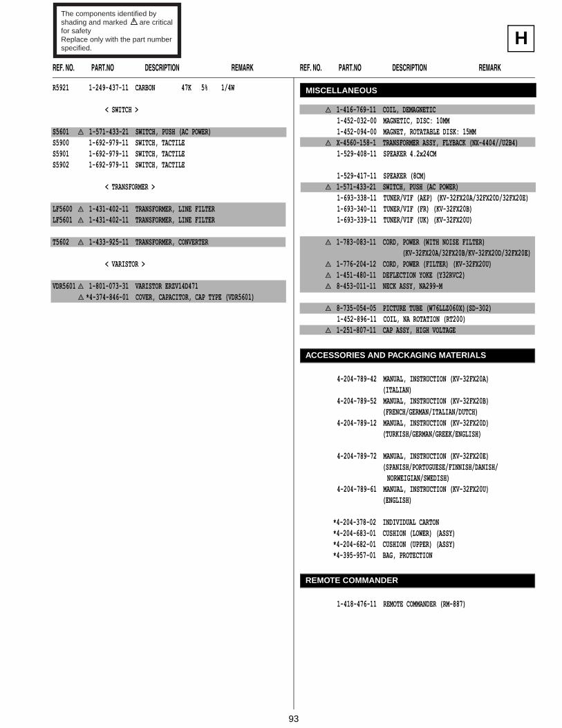
REF. NO. PART.NO DESCRIPTION REMARK REF. NO. PART.NO DESCRIPTION REMARK
The components identified byshading and marked are criticalfor safetyReplace only with the part numberspecified.
H
R5921 1-249-437-11 CARBON 47K 5% 1/4W
< SWITCH >
S5601 £ 1-571-433-21 SWITCH, PUSH (AC POWER)S5900 1-692-979-11 SWITCH, TACTILES5901 1-692-979-11 SWITCH, TACTILES5902 1-692-979-11 SWITCH, TACTILE
< TRANSFORMER >
LF5600 £ 1-431-402-11 TRANSFORMER, LINE FILTERLF5601 £ 1-431-402-11 TRANSFORMER, LINE FILTER
T5602 £ 1-433-925-11 TRANSFORMER, CONVERTER
< VARISTOR >
VDR5601 £ 1-801-073-31 VARISTOR ERZV14D471 £ *4-374-846-01 COVER, CAPACITOR, CAP TYPE (VDR5601)
£ 1-416-769-11 COIL, DEMAGNETIC 1-452-032-00 MAGNETIC, DISC: 10MM 1-452-094-00 MAGNET, ROTATABLE DISK: 15MM £ X-4560-158-1 TRANSFORMER ASSY, FLYBACK (NX-4404//U2B4) 1-529-408-11 SPEAKER 4.2x24CM
1-529-417-11 SPEAKER (8CM) £ 1-571-433-21 SWITCH, PUSH (AC POWER) 1-693-338-11 TUNER/VIF (AEP) (KV-32FX20A/32FX20D/32FX20E) 1-693-340-11 TUNER/VIF (FR) (KV-32FX20B) 1-693-339-11 TUNER/VIF (UK) (KV-32FX20U) £ 1-783-083-11 CORD, POWER (WITH NOISE FILTER) (KV-32FX20A/32FX20B/KV-32FX20D/32FX20E) £ 1-776-204-12 CORD, POWER (FILTER) (KV-32FX20U) £ 1-451-480-11 DEFLECTION YOKE (Y32RVC2) £ 8-453-011-11 NECK ASSY, NA299-M
£ 8-735-054-05 PICTURE TUBE (W76LLZ060X)(SD-302) 1-452-896-11 COIL, NA ROTATION (RT200) £ 1-251-807-11 CAP ASSY, HIGH VOLTAGE
4-204-789-42 MANUAL, INSTRUCTION (KV-32FX20A) (ITALIAN) 4-204-789-52 MANUAL, INSTRUCTION (KV-32FX20B) (FRENCH/GERMAN/ITALIAN/DUTCH) 4-204-789-12 MANUAL, INSTRUCTION (KV-32FX20D) (TURKISH/GERMAN/GREEK/ENGLISH)
4-204-789-72 MANUAL, INSTRUCTION (KV-32FX20E) (SPANISH/PORTUGUESE/FINNISH/DANISH/ NORWEIGIAN/SWEDISH) 4-204-789-61 MANUAL, INSTRUCTION (KV-32FX20U) (ENGLISH)
*4-204-378-02 INDIVIDUAL CARTON *4-204-683-01 CUSHION (LOWER) (ASSY) *4-204-682-01 CUSHION (UPPER) (ASSY) *4-395-957-01 BAG, PROTECTION
1-418-476-11 REMOTE COMMANDER (RM-887)
ACCESSORIES AND PACKAGING MATERIALS
REMOTE COMMANDER
MISCELLANEOUS
93