Embed Size (px)
Citation preview

FEATURES SERIAL INPUT
–92dB MAX THD: FS Input, K Grade
–74dB MAX THD: –20dB Input, K Grade
96dB DYNAMIC RANGE
NO EXTERNAL COMPONENTS REQUIRED
16-BIT RESOLUTION
15-BIT MONOTONICITY, TYP
0.001% OF FSR TYP DIFFERENTIALLINEARITY ERROR
1.5µs SETTLING TIME, TYP: Voltage Out
±3V OR ±1mA AUDIO OUTPUT
EIAJ STC-007-COMPATIBLE
OPERATES ON ±5V TO ±12V SUPPLIES
PINOUT ALLOWS I OUT OPTION
PLASTIC DIP OR SOIC PACKAGE
This converter is completely self-contained with astable, low noise, internal zener voltage reference;high speed current switches; a resistor ladder net-work; and a fast settling, low noise output operationalamplifier all on a single monolithic chip. Theconverters are operated using two power supplies thatcan range from ±5V to ±12V. Power dissipation with±5V supplies is typically less than 200mW. Alsoincluded is a provision for external adjustment of theMSB error (differential linearity error at bipolar zero)to further improve total harmonic distortion (THD)specifications if desired. Few external componentsare necessary for operation, and all criticalspecifications are 100% tested. This helps assure theuser of high system reliability and outstanding overallsystem performance.
The PCM56 is packaged in a high-quality 16-pinmolded plastic DIP package or SOIC and has passedoperating life tests under simultaneous high-pressure,high-temperature, and high-humidity conditions.
DESIGNED FOR AUDIO
PCM56PPCM56U
®
International Airport Industrial Park • Mailing Address: PO Box 11400 • Tucson, AZ 85734 • Street Address: 6730 S. Tucson Blvd. • Tucson, AZ 85706Tel: (520) 746-1111 • Twx: 910-952-1111 • Cable: BBRCORP • Telex: 066-6491 • FAX: (520) 889-1510 • Immediate Product Info: (800) 548-6132
DESCRIPTIONThe PCM56 is a state-of-the-art, fully monotonic,digital-to-analog converter that is designed andspecified for digital audio applications. This deviceemploys ultra-stable nichrome (NiCr) thin-filmresistors to provide monotonicity, low distortion, andlow differential linearity error (especially aroundbipolar zero) over long periods of time and over thefull operating temperature.
RF
Audio Output
Reference 16-Bit IOUT DAC
16-Bit Input Latch
16-Bit Serial-to-Parallel Conversion
Clock LE Data
Serial Input 16-Bit MonolithicDIGITAL-TO-ANALOG CONVERTER
©1987 Burr-Brown Corporation PDS-700D Printed in U.S.A. August, 1993
SBAS149
2®
PCM56
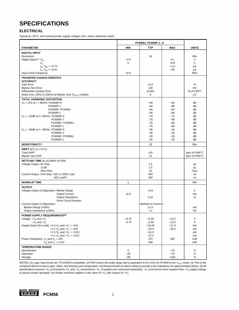
DIGITAL INPUTResolution 16 BitsDigital Inputs(1): VIH +2.4 +VL V
VIL 0 +0.8 VIIH, VIN = +2.7V +1.0 µAIIL, VIN = +0.4V –50 µA
Input Clock Frequency 10.0 MHz
TRANSFER CHARACTERISTICSACCURACYGain Error ±2.0 %Bipolar Zero Error ±30 mVDifferential Linearity Error ±0.001 % of FSR(2)
Noise (rms, 20Hz to 20kHz) at Bipolar Zero (VOUT models) 6 µV
TOTAL HARMONIC DISTORTIONVO = ±FS at f = 991Hz: PCM56P-K –94 –92 dB
PCM56P-J –94 –88 dBPCM56P, PCM56U –94 –82 dBPCM56P-L –94 –80 dB
VO = –20dB at f = 991Hz: PCM56P-K –75 –74 dBPCM56P-J –75 –68 dBPCM56P, PCM56U –75 –68 dBPCM56P-L –75 –60 dB
VO = –60dB at f = 991Hz: PCM56P-K –35 –34 dBPCM56P-J –35 –28 dBPCM56P, PCM56U –35 –28 dBPCM56P-L –35 –20 dB
MONOTONICITY 15 Bits
DRIFT (0°C to +70°C)Total Drift(3) ±25 ppm of FSR/°CBipolar Zero Drift ±4 ppm of FSR/°C
SETTLING TIME (to ±0.006% of FSR)Voltage Output: 6V Step 1.5 µs
1LSB 1.0 µsSlew Rate 10 V/µs
Current Output, 1mA Step: 10Ω to 100Ω Load 350 ns1kΩ Load(4) 350 ns
WARM-UP TIME 1 Min
OUTPUTVoltage Output Configuration: Bipolar Range ±3.0 V
Output Current ±2.0 mAOutput Impedance 0.10 ΩShort Circuit Duration
Current Output Configuration:Bipolar Range (±30%) ±1.0 mAOutput Impedance (±30%) 1.2 kΩ
POWER SUPPLY REQUIREMENTS(5)
Voltage: +VS and +VL +4.75 +5.00 +13.2 V–VS and –VL –4.75 –5.00 –13.2 V
Supply Drain (No Load): +V (+VS and +VL = +5V) +10.00 +17.0 mA–V (–VS and –VL = –5V) –25.0 –35.0 mA+V (+VS and +VL = +12V) +12.0 mA–V (–VS and –VL = –12V) –27.0 mA
Power Dissipation: VS and VL = ±5V 175 260 mWVS and VL = ±12V 468 mW
TEMPERATURE RANGESpecification 0 +70 °COperation –25 +70 °CStorage –60 +100 °C
NOTES: (1) Logic input levels are TTL/CMOS-compatible. (2) FSR means full-scale range and is equivalent to 6V (±3V) for PCM56 in the VOUT mode. (3) This is thecombined drift error due to gain, offset, and linearity over temperature. (4) Measured with an active clamp to provide a low impedance for approximately 200ns. (5) Allspecifications assume +VS connected to +VL and –VS connected to –VL. If supplies are connected separately, –VL must not be more negative than –VS supply voltageto assure proper operation. No similar restriction applies to the value of +VL with respect to +VS.
PCM56U, PCM56P-J, -K
PARAMETER MIN TYP MAX UNITS
SPECIFICATIONSELECTRICALTypical at +25°C, and nominal power supply voltages ±5V, unless otherwise noted.
Indefinite to Common
3®
PCM56
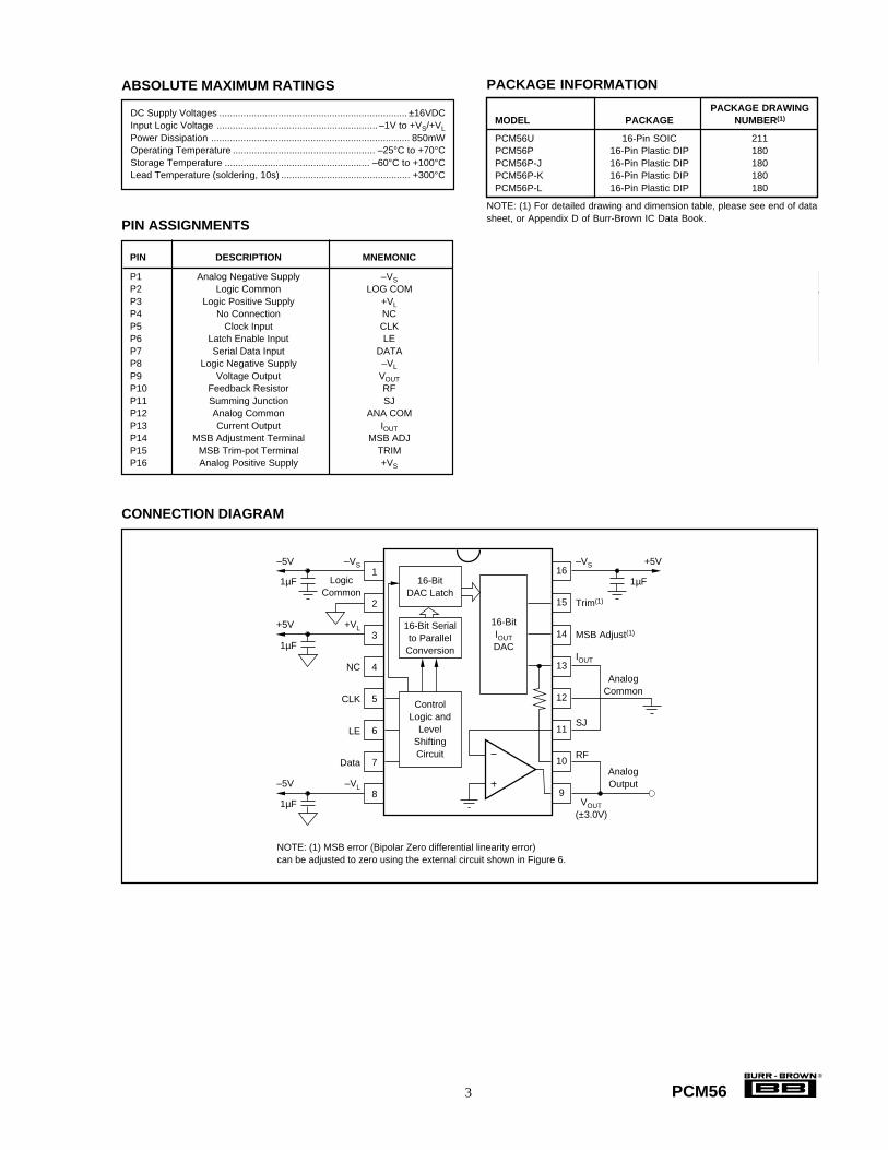
DC Supply Voltages ...................................................................... ±16VDCInput Logic Voltage ............................................................ –1V to +VS/+VL
Power Dissipation .......................................................................... 850mWOperating Temperature ..................................................... –25°C to +70°CStorage Temperature ...................................................... –60°C to +100°CLead Temperature (soldering, 10s) ................................................ +300°C
ABSOLUTE MAXIMUM RATINGS PACKAGE INFORMATION
PACKAGE DRAWINGMODEL PACKAGE NUMBER (1)
PCM56U 16-Pin SOIC 211PCM56P 16-Pin Plastic DIP 180PCM56P-J 16-Pin Plastic DIP 180PCM56P-K 16-Pin Plastic DIP 180PCM56P-L 16-Pin Plastic DIP 180
NOTE: (1) For detailed drawing and dimension table, please see end of datasheet, or Appendix D of Burr-Brown IC Data Book.
PIN DESCRIPTION MNEMONIC
P1 Analog Negative Supply –VSP2 Logic Common LOG COMP3 Logic Positive Supply +VLP4 No Connection NCP5 Clock Input CLKP6 Latch Enable Input LEP7 Serial Data Input DATAP8 Logic Negative Supply –VL
P9 Voltage Output VOUTP10 Feedback Resistor RFP11 Summing Junction SJP12 Analog Common ANA COMP13 Current Output IOUTP14 MSB Adjustment Terminal MSB ADJP15 MSB Trim-pot Terminal TRIMP16 Analog Positive Supply +VS
PIN ASSIGNMENTS
CONNECTION DIAGRAM
16-Bit DAC Latch
16-Bit Serial to Parallel
Conversion
Control Logic and
Level Shifting Circuit
1
2
3
4
5
6
7
8
16
15
14
13
12
11
10
9
16-Bit IOUT DAC
–5V
+5V
–5V
1µF
1µF
1µF Logic Common
–VS
+VL
NC
CLK
LE
Data
–VL
–VS
Analog Common
SJ
RF
VOUT (±3.0V)
Trim(1)
MSB Adjust(1)
IOUT
Analog Output
1µF
+5V
NOTE: (1) MSB error (Bipolar Zero differential linearity error) can be adjusted to zero using the external circuit shown in Figure 6.
4®
PCM56
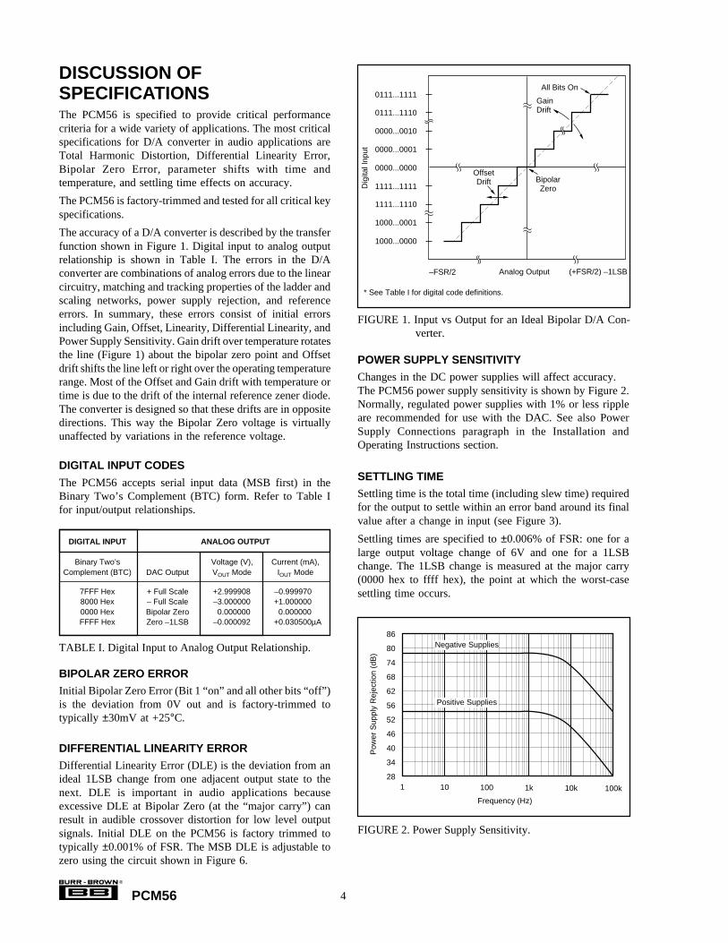
DISCUSSION OFSPECIFICATIONSThe PCM56 is specified to provide critical performancecriteria for a wide variety of applications. The most criticalspecifications for D/A converter in audio applications areTotal Harmonic Distortion, Differential Linearity Error,Bipolar Zero Error, parameter shifts with time andtemperature, and settling time effects on accuracy.
The PCM56 is factory-trimmed and tested for all critical keyspecifications.
The accuracy of a D/A converter is described by the transferfunction shown in Figure 1. Digital input to analog outputrelationship is shown in Table I. The errors in the D/Aconverter are combinations of analog errors due to the linearcircuitry, matching and tracking properties of the ladder andscaling networks, power supply rejection, and referenceerrors. In summary, these errors consist of initial errorsincluding Gain, Offset, Linearity, Differential Linearity, andPower Supply Sensitivity. Gain drift over temperature rotatesthe line (Figure 1) about the bipolar zero point and Offsetdrift shifts the line left or right over the operating temperaturerange. Most of the Offset and Gain drift with temperature ortime is due to the drift of the internal reference zener diode.The converter is designed so that these drifts are in oppositedirections. This way the Bipolar Zero voltage is virtuallyunaffected by variations in the reference voltage.
DIGITAL INPUT CODES
The PCM56 accepts serial input data (MSB first) in theBinary Two’s Complement (BTC) form. Refer to Table Ifor input/output relationships.
FIGURE 1. Input vs Output for an Ideal Bipolar D/A Con-verter.
BIPOLAR ZERO ERROR
Initial Bipolar Zero Error (Bit 1 “on” and all other bits “off”)is the deviation from 0V out and is factory-trimmed totypically ±30mV at +25°C.
DIFFERENTIAL LINEARITY ERROR
Differential Linearity Error (DLE) is the deviation from anideal 1LSB change from one adjacent output state to thenext. DLE is important in audio applications becauseexcessive DLE at Bipolar Zero (at the “major carry”) canresult in audible crossover distortion for low level outputsignals. Initial DLE on the PCM56 is factory trimmed totypically ±0.001% of FSR. The MSB DLE is adjustable tozero using the circuit shown in Figure 6.
POWER SUPPLY SENSITIVITY
Changes in the DC power supplies will affect accuracy.The PCM56 power supply sensitivity is shown by Figure 2.Normally, regulated power supplies with 1% or less rippleare recommended for use with the DAC. See also PowerSupply Connections paragraph in the Installation andOperating Instructions section.
SETTLING TIME
Settling time is the total time (including slew time) requiredfor the output to settle within an error band around its finalvalue after a change in input (see Figure 3).
Settling times are specified to ±0.006% of FSR: one for alarge output voltage change of 6V and one for a 1LSBchange. The 1LSB change is measured at the major carry(0000 hex to ffff hex), the point at which the worst-casesettling time occurs.
DIGITAL INPUT ANALOG OUTPUT
Binary Two’s Voltage (V), Current (mA),Complement (BTC) DAC Output VOUT Mode IOUT Mode
7FFF Hex + Full Scale +2.999908 –0.9999708000 Hex – Full Scale –3.000000 +1.0000000000 Hex Bipolar Zero 0.000000 0.000000FFFF Hex Zero –1LSB –0.000092 +0.030500µA
TABLE I. Digital Input to Analog Output Relationship.
Frequency (Hz)
1
86
80
74
68
62
56
52
46
40
34
28
Pow
er S
uppl
y R
ejec
tion
(dB
)
10 100 1k 10k 100k
Negative Supplies
Positive Supplies
FIGURE 2. Power Supply Sensitivity.
Gain Drift
Offset Drift Bipolar
Zero
0111...1111
0111...1110
0000...0010
0000...0001
0000...0000
1111...1111
1111...1110
1000...0001
1000...0000
Dig
ital I
nput
–FSR/2 Analog Output (+FSR/2) –1LSB
All Bits On
* See Table I for digital code definitions.

5®
PCM56
STABILITY WITH TIME AND TEMPERATURE
The parameters of a D/A converter designed for audioapplications should be stable over a relatively widetemperature range and over long periods of time to avoidundesirable periodic readjustment. The most importantparameters are Bipolar Zero Error, Differential LinearityError, and Total Harmonic Distortion. Most of the Offsetand Gain drift with temperature or time is due to the drift ofthe internal reference zener diode. The PCM56 is designedso that these drifts are in opposite directions so that theBipolar Zero voltage is virtually unaffected by variations inthe reference voltage. Both DLE and THD are dependentupon the matching and tracking of resistor ratios and uponVBE and hFE of the current-source transistors. The PCM56was designed so that any absolute shift in these componentshas virtually no effect on DLE or THD. The resistors aremade of identical links of ultra-stable nichrome thin-film.The current density in these resistors is very low to furtherenhance their stability.
DYNAMIC RANGE
The Dynamic Range is a measure of the ratio of the smallestsignals the converter can produce to the full-scale range andis usually expressed in decibels (dB). The theoretical dynamicrange of a converter is approximately 6 x n, or about 96dBof a 16-bit converter. The actual, or useful, dynamic range islimited by noise and linearity errors and is therefore somewhatless than the theoretical limit. However, this does point outthat a resolution of at least 16 bits is required to obtain a90dB minimum dynamic range, regardless of the accuracyof the converter. Another specification that is useful foraudio applications is Total Harmonic Distortion.
TOTAL HARMONIC DISTORTION
THD is useful in audio applications and is a measure of themagnitude and distribution of the Linearity Error, DifferentialLinearity Error, and Noise, as well as Quantization Error. Tobe useful, THD should be specified for both high level andlow level input signals. This error is unadjustable and is themost meaningful indicator of D/A converter accuracy foraudio applications.
FIGURE 3. Full Scale Range Settling Time vs Accuracy.
Settling Time (µs)
0.01
1.0
0.3
0.1
0.03
0.01
0.003
0.001
Acc
urac
y P
erce
nt F
ull-S
cale
Ran
ge (
%)
RL = 200Ω
0.1 1.0 10.0
Current Output Mode
Voltage Output Mode
The THD is defined as the ratio of the square root of the sumof the squares of the values of the harmonics to the value ofthe fundamental input frequency and is expressed in percentor dB. The rms value of the PCM56 error referred to theinput can be shown to be:
where n is the number of samples in one cycle of any givensine wave, EL(i) is the linearity error of the PCM56 at eachsampling point, and EQ(i) is the quantization error at eachsampling point. The THD can then be expressed as:
= 100%Erms
where Erms is the rms signal-voltage level.
This expression indicates that, in general, there is a correlationbetween the THD and the square root of the sum of thesquares of the linearity errors at each digital word of interest.However, this expression does not mean that the worst-caselinearity error of the D/A is directly correlated to the THD.
For the PCM56 the test period was chosen to be 22.7µs(44.1kHz), which is compatible with the EIAJ STC-007specification for PCM audio. The test frequency is 991Hzand the amplitude of the input signal is 0dB, –20dB, and–60dB down from full scale.
Figure 4 shows the typical THD as a function of outputvoltage.
Figure 5 shows typical THD as a function of frequency.
(1)∈ rms = 1/n EL
(i ) + EQ
(i) 2
i = 1
n
∑
1/n EL
(i ) + EQ
(i) 2
i = 1
n
∑ (2)
THD = ∈ rms / E rms
FIGURE 4. Total Harmonic Distortion (THD) vs VOUT.
X
VOUT (dB)
–60
10.0
Tot
al H
arm
onic
Dis
tort
ion
(%)
0dB = Full Scale Range (FSR)
–60 –50 –40 –30 –20 –10 0
1.0
0.1
0.01
0.001
14 Bits
16 Bits

6®
PCM56
FIGURE 5. Total Harmonic Distortion (THD) vs Frequency.
INSTALLATION ANDOPERATING INSTRUCTIONSPOWER SUPPLY CONNECTIONS
For optimum performance and noise rejection, power supplydecoupling capacitors should be added as shown in theConnection Diagram. These capacitors (1µF tantalum orelectrolytic recommended) should be located close to theconverter.
MSB ERROR ADJUSTMENT PROCEDURE
(OPTIONAL)
The MSB error of the PCM56 can be adjusted to make thedifferential linearity error (DLE) at BPZ essentially zero.This is important when the signal output levels are very low,because zero crossing noise (DLE at BPZ) becomes verysignificant when compared to the small code changesoccurring in the LSB portion of the converter.
Differential linearity error at bipolar zero and THD areguaranteed to meet data sheet specifications without anyexternal adjustment. However, a provision has been madefor an optional adjustment of the MSB linearity point whichmakes it possible to eliminate DLE error at BPZ. Twoprocedures are given to allow either static or dynamicadjustment. The dynamic procedure is preferred because ofthe difficulty associated with the static method (accuratelymeasuring 16-bit LSB steps).
To statically adjust DLE at BPZ, refer to the circuit shownin Figure 6, or the PCM56 connection diagram.
After allowing ample warm-up time (5-10 minutes) to assurestable operation of the PCM56, select input code FFFFhexadecimal (all bits on except the MSB). Measure theaudio output voltage using a 6-1/2 digit voltmeter and recordit. Change the digital input code to 0000 hexadecimal (allbits off except the MSB). Adjust the 100kΩ potentiometer tomake the audio output read 92µV more than the voltagereading of the previous code (a 1LSB step = 92µV).
A much simpler method is to dynamically adjust the DLE atBPZ. Again, refer to Figure 6 for circuitry and componentvalues. Assuming the device has been installed in a digitalaudio application circuit, send the appropriate digital inputto produce a –80dB level sinusoidal output. While measuringthe THD of the audio circuit output, adjust the 100kΩpotentiometer until a minimum level of distortion is observed.
INPUT TIMING CONSIDERATIONS
Figure 7 and 8 refer to the input timing required to interfacethe inputs of PCM56 to a serial input data stream. Serial datais accepted in Binary Two’s Complement (BTC) with theMSB being loaded first. Data is clocked in on positive goingclock (CLK) edges and is latched into the DAC inputregister on negative going latch enable (LE) edges.
The latch enable input must be high for at least one clockcycle before going low, and then must be held low for atleast one clock cycle. The last 16 data bits clocked into theserial input register are the ones that are transferred to theDAC input register when latch enable goes low. In otherwords, when more than 16 clock cycles occur between alatch enable, only the data present during the last 16 clockswill be transferred to the DAC input register.
One requirement for clocking in all 16 bits is the necessityfor a “17th” clock pulse. This automatically occurs when theclock is continuous (last bit shifts in on the first bit of thenext data word). If the clock is stopped between input of 16-bit data words, the latch enable (LE) must remain low untilafter the first clock of the next 16-bit data word stream. Thisensures that the latch is properly set up.
Figure 7 refers to the general input format required for thePCM56. Figure 8 shows the specific relationships betweenthe various signals and their timing constraints.
INSTALLATIONCONSIDERATIONSIf the optional external MSB error circuitry is used, apotentiometer with adequate resolution and a TCR of 100ppm/°C or less is required. Also, extra care must be taken toinsure that no leakage path (either AC or DC) exists to pin14. If the circuit is not used, pins 14 and 15 should be leftopen.
The PCM converter and the wiring to its connectors shouldbe located to provide the optimum isolation from sources ofRFI and EMI. The important consideration in the elimination
FIGURE 6. MSB Adjustment Circuit.
Frequency (Hz)
100
0.1T
otal
Har
mon
ic D
isto
rtio
n (%
)
0.01
0.0011k 10k 20k
(Full Scale)
(–20dB)
470kΩ 100kΩ 200kΩTrim 15
MSB Adjust 14
1 –VS

7®
PCM56
FIGURE 7. Input Timing Diagram.
FIGURE 8. Input Timing Relationships.
source and drain of the FET switch operate at a virtualground when “C” and “B” are connected in the samplemode, there is no increase in distortion caused by themodulation effect of RON by the audio signal.
Figure 10 shows the deglitcher controls for both left andright channels which are produced by timing control logic.A delay of 1.5µs (tω) is provided to allow the output of thePCM56 to settle within a small error band around its finalvalue before connecting it to the channel output. Due to thefast settling time of the PCM56 it is possible to minimize thedelay between the left- and right-channel outputs whenusing a single D/A converter for both channels. This isimportant because the right- and left-channel data are recordedin-phase and the use of the slower D/A converter wouldresult in significant phase error at higher frequencies.
The obvious solution to the phase shift problem in a two-channel system would be to use two D/A converters (one perchannel) and time the outputs to change simultaneously.Figure 11 shows a block diagram of the final test circuitryused for PCM56. It should be noted that no deglitchingcircuitry is required on the DAC output to meet specifiedTHD performance. This means that when one PCM56 isused per channel, the need for all the sample/hold andcontrols circuitry associated with a single DAC (two-channel)design is effectively eliminated. The PCM56 is tested tomeet its THD specifications without the need for outputdeglitching.
A low-pass filter is required after the PCM56 to remove allunwanted frequency components caused by the samplingfrequency as well as those resulting from the discrete natureof the D/A output. This filter must have a flat frequencyresponse over the entire audio band (0-20kHz) and a veryhigh attenuation above 20kHz.
Most previous digital audio circuits used a higher order (9-13 pole) analog filter. However, the phase response of ananalog filter with these amplitude characteristics is nonlinearand can disturb the pulse-shaped characteristic transientscontained in music.
of RF radiation or pickup is loop area; therefore, signal leadsand their return conductors should be kept close together.This reduces the external magnetic field along with anyradiation. Also, if a signal lead and its return conductor arewired close together, they represent a small flux-capturecross section for any external field. This reduces radiationpickup in the circuit.
APPLICATIONSFigures 9 and 10 show a circuit and timing diagram for asingle PCM56 used to obtain both left- and right-channeloutput in a typical digital audio system. The audio output ofthe PCM56 is alternately time-shared between the left andright channels. The design is greatly simplified because thePCM56 is a complete D/A converter requiring no externalreference or output op amp.
A sample/hold (S/H) amplifier, or “deglitcher” is required atthe output of the D/A for both the left and right channel, asshown in Figure 9. The S/H amplifier for the left channel iscomposed of A1, SW1, and associated circuitry. A1 is usedas an integrator to hold the analog voltage in C1. Since the
Data
Latch Enable
2(2)
Clock
(3)
MSB LSB
MSB
(4)
(1)
NOTES: (1) If clock is stopped between input of 16-bit data words, latch enable (LE) must remain low until after the first clock of the next 16-bit data word stream. (2) Data format is binary two's complement (BTC). Individual data bits are clocked in on the corresponding positive clock edge. (3) Latch enable (LE) must remain low at least one clock cycle after going negative. (4) Latch enable (LE) must be high for at least one clock cycle before going negative.
116151413121110987654321
MSBData Input
> 40ns
> One Clock Cycle
Latch Enable
> One Clock Cycle
Clock Input
> 40ns > 5ns
> 100ns
> 15ns
LSB
>15ns >15ns
> 40ns

8®
PCM56
SECOND GENERATION SYSTEMS
One method of avoiding the problems associated with ahigher order analog filter would be to use digital filteroversampling techniques. Oversampling by a factor of twowould move the sampling frequency (88.2kHz) out to apoint where only a simple low-order phase-linear analogfilter is required after the deglitcher output to removeunwanted intermodulation products. In a digital compactdisc application, various VLSI chips perform the functionsof error detection/correction, digital filtering, and formattingof the digital information to provide the clock, latch enable,and serial input to the PCM56. These VLSI chips are
available from several sources (Sony, Yamaha, Signetics,etc.) and are specifically optimized for digital audioapplications.
Oversampled circuitry requires a very fast D/A convertersince the sampling frequency is multiplied by a factor of twoor more (for each output channel). A single PCM56 canprovide two-channel oversampling at a 4X rate (176.4kHz/channel) and still remain well within the settling timerequirements for maintaining specified THD performance.This would reduce the complexities of the analog filter evenfurther from that used in 2X oversampling circuitry.
FIGURE 9. A Sample/Hold Amplifier (Deglitcher) is Required at the Digital-to-Analog Output for Both Left and Right Channels.
FIGURE 10. Timing Diagram for the Deglitcher Control Signals.
R2 2.2kΩ
A1(1)
C1 680pFC
BA
Left Channel Output to LPF
SW1
MP7512 (Micro Power)
R4 2.2kΩ
A2(1)
C2 680pFC
BA
Right Channel Output to LPF
SW2
MP7512 (Micro Power)
R1 2.2kΩ
R3 2.2kΩ
NOTE: (1) 1 OPA101AM or 1/4 OPA404KP or 1 OPA606KP or OPA2604.
PCM56
Serial Data
Clock
Latch Enable
Left Channel Deglitcher Control
Right Channel Deglitcher Control
A "low" signal on the deglitcher control closes switch "A", while a "high" signal closes switch "B".
Latch Enable
Right ChannelSerial Data
44.1kHz
Left Channel Left Channel Right Channel
Right Channel Deglitcher Control
Left Channel Deglitcher Control
t DELAY 4.5µs max
t = 1.5µs DAC Settling Timeω
The deglitcher control signals by timing control logic. The fast settling time of the PCM56 makes it possible to minimize the delay between left and right channels to about 4.5µs, which reduces phase error at the higher audio frequencies.

9®
PCM56
The information provided herein is believed to be reliable; however, BURR-BROWN assumes no responsibility for inaccuracies or omissions. BURR-BROWN assumesno responsibility for the use of this information, and all use of such information shall be entirely at the user's own risk. Prices and specifications are subject to changewithout notice. No patent rights or licenses to any of the circuits described herein are implied or granted to any third party. BURR-BROWN does not authorize or warrantany BURR-BROWN product for use in life support devices and/or systems.
FIGURE 11. Block Diagram of Distortion Test Circuit.
Distortion Analyzer
(Shiba Soku Model 725 or Equivalent)
Programmable Gain Amp
0dB to 60dB
Low-Pass Filter
(Toko APQ-25 or Equivalent)
DUT (PCM58P)
Parallel-to-Serial Conversion
Digital Code (EPROM)
Binary Counter
Timing Logic
Clock
Latch Enable
Sampling Rate = 44.1kHz x 4 (176.4kHz) Output Frequency = 991Hz
Use 400Hz High-Pass Filter and 30kHz Low-Pass Filter Meter Settings
LOW-PASS FILTER CHARACTERISTIC
0
–20
–40
–60
–80
–100
–120
Gai
n (d
B)
Frequency (Hz)1 10 10 10 10 101 2 3 4 5
PACKAGE OPTION ADDENDUM
www.ti.com 25-Jan-2016
Addendum-Page 1
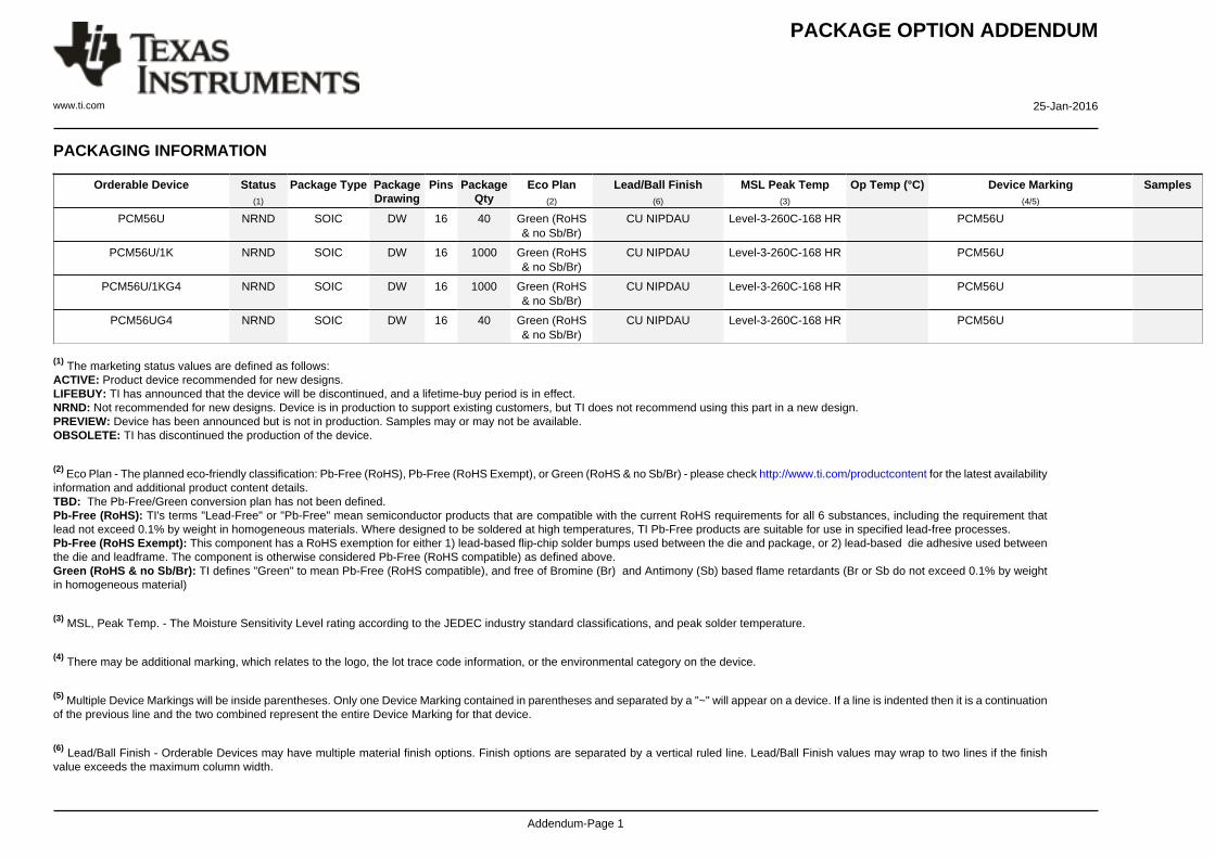
PACKAGING INFORMATION
Orderable Device Status(1)
Package Type PackageDrawing
Pins PackageQty
Eco Plan(2)
Lead/Ball Finish(6)
MSL Peak Temp(3)
Op Temp (°C) Device Marking(4/5)
Samples
PCM56U NRND SOIC DW 16 40 Green (RoHS& no Sb/Br)
CU NIPDAU Level-3-260C-168 HR PCM56U
PCM56U/1K NRND SOIC DW 16 1000 Green (RoHS& no Sb/Br)
CU NIPDAU Level-3-260C-168 HR PCM56U
PCM56U/1KG4 NRND SOIC DW 16 1000 Green (RoHS& no Sb/Br)
CU NIPDAU Level-3-260C-168 HR PCM56U
PCM56UG4 NRND SOIC DW 16 40 Green (RoHS& no Sb/Br)
CU NIPDAU Level-3-260C-168 HR PCM56U
(1) The marketing status values are defined as follows:ACTIVE: Product device recommended for new designs.LIFEBUY: TI has announced that the device will be discontinued, and a lifetime-buy period is in effect.NRND: Not recommended for new designs. Device is in production to support existing customers, but TI does not recommend using this part in a new design.PREVIEW: Device has been announced but is not in production. Samples may or may not be available.OBSOLETE: TI has discontinued the production of the device.
(2) Eco Plan - The planned eco-friendly classification: Pb-Free (RoHS), Pb-Free (RoHS Exempt), or Green (RoHS & no Sb/Br) - please check http://www.ti.com/productcontent for the latest availabilityinformation and additional product content details.TBD: The Pb-Free/Green conversion plan has not been defined.Pb-Free (RoHS): TI's terms "Lead-Free" or "Pb-Free" mean semiconductor products that are compatible with the current RoHS requirements for all 6 substances, including the requirement thatlead not exceed 0.1% by weight in homogeneous materials. Where designed to be soldered at high temperatures, TI Pb-Free products are suitable for use in specified lead-free processes.Pb-Free (RoHS Exempt): This component has a RoHS exemption for either 1) lead-based flip-chip solder bumps used between the die and package, or 2) lead-based die adhesive used betweenthe die and leadframe. The component is otherwise considered Pb-Free (RoHS compatible) as defined above.Green (RoHS & no Sb/Br): TI defines "Green" to mean Pb-Free (RoHS compatible), and free of Bromine (Br) and Antimony (Sb) based flame retardants (Br or Sb do not exceed 0.1% by weightin homogeneous material)
(3) MSL, Peak Temp. - The Moisture Sensitivity Level rating according to the JEDEC industry standard classifications, and peak solder temperature.
(4) There may be additional marking, which relates to the logo, the lot trace code information, or the environmental category on the device.
(5) Multiple Device Markings will be inside parentheses. Only one Device Marking contained in parentheses and separated by a "~" will appear on a device. If a line is indented then it is a continuationof the previous line and the two combined represent the entire Device Marking for that device.
(6) Lead/Ball Finish - Orderable Devices may have multiple material finish options. Finish options are separated by a vertical ruled line. Lead/Ball Finish values may wrap to two lines if the finishvalue exceeds the maximum column width.
PACKAGE OPTION ADDENDUM
www.ti.com 25-Jan-2016
Addendum-Page 2
Important Information and Disclaimer:The information provided on this page represents TI's knowledge and belief as of the date that it is provided. TI bases its knowledge and belief on informationprovided by third parties, and makes no representation or warranty as to the accuracy of such information. Efforts are underway to better integrate information from third parties. TI has taken andcontinues to take reasonable steps to provide representative and accurate information but may not have conducted destructive testing or chemical analysis on incoming materials and chemicals.TI and TI suppliers consider certain information to be proprietary, and thus CAS numbers and other limited information may not be available for release.
In no event shall TI's liability arising out of such information exceed the total purchase price of the TI part(s) at issue in this document sold by TI to Customer on an annual basis.

TAPE AND REEL INFORMATION
*All dimensions are nominal
Device PackageType
PackageDrawing
Pins SPQ ReelDiameter
(mm)
ReelWidth
W1 (mm)
A0(mm)
B0(mm)
K0(mm)
P1(mm)
W(mm)
Pin1Quadrant
PCM56U/1K SOIC DW 16 1000 330.0 16.4 10.75 10.7 2.7 12.0 16.0 Q1
PACKAGE MATERIALS INFORMATION
www.ti.com 26-Jan-2013
Pack Materials-Page 1

*All dimensions are nominal
Device Package Type Package Drawing Pins SPQ Length (mm) Width (mm) Height (mm)
PCM56U/1K SOIC DW 16 1000 367.0 367.0 38.0
PACKAGE MATERIALS INFORMATION
www.ti.com 26-Jan-2013
Pack Materials-Page 2
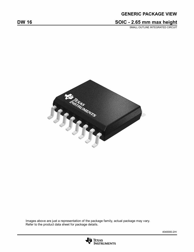
GENERIC PACKAGE VIEW
Images above are just a representation of the package family, actual package may vary.Refer to the product data sheet for package details.
DW 16 SOIC - 2.65 mm max heightSMALL OUTLINE INTEGRATED CIRCUIT
4040000-2/H
www.ti.com
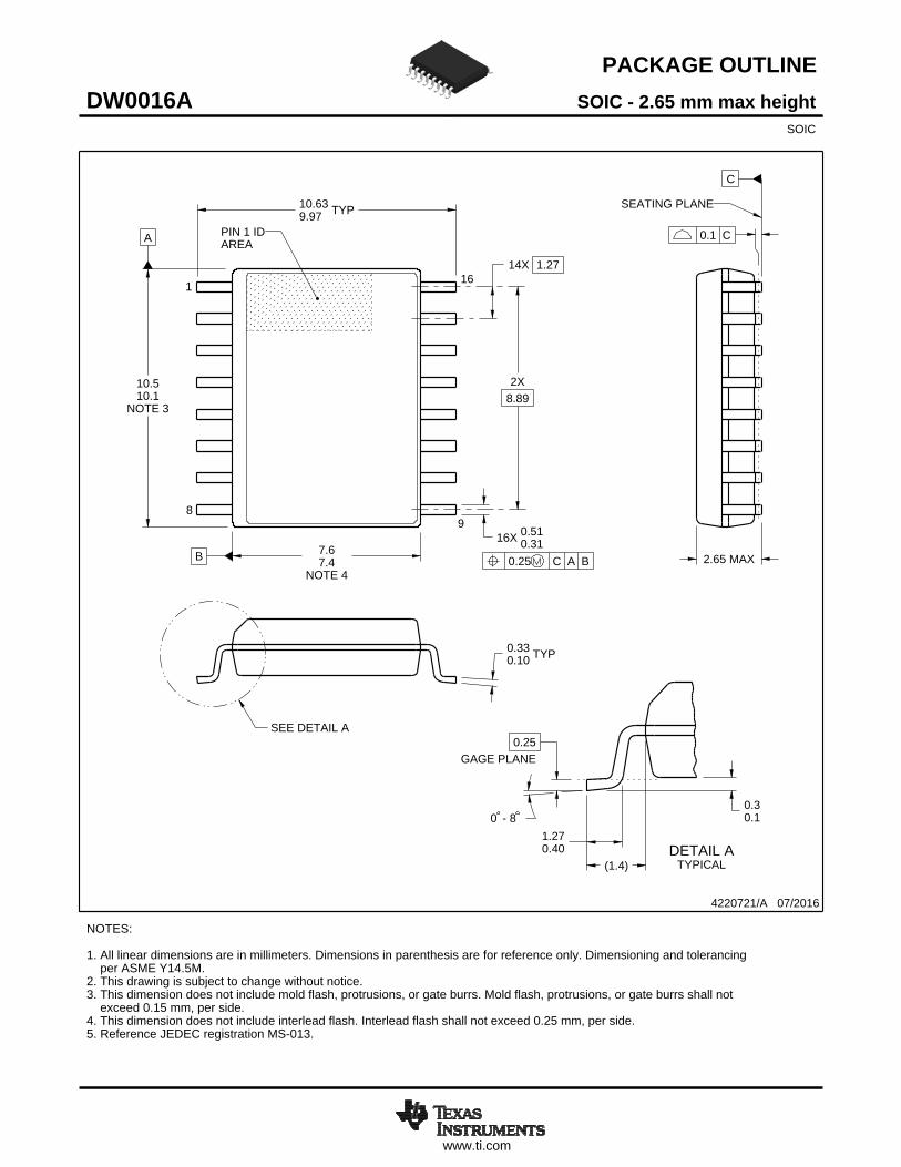
PACKAGE OUTLINE
C
TYP10.639.97
2.65 MAX
14X 1.27
16X 0.510.31
2X8.89
TYP0.330.10
0 - 80.30.1
(1.4)
0.25GAGE PLANE
1.270.40
A
NOTE 3
10.510.1
BNOTE 4
7.67.4
4220721/A 07/2016
SOIC - 2.65 mm max heightDW0016ASOIC
NOTES: 1. All linear dimensions are in millimeters. Dimensions in parenthesis are for reference only. Dimensioning and tolerancing per ASME Y14.5M. 2. This drawing is subject to change without notice. 3. This dimension does not include mold flash, protrusions, or gate burrs. Mold flash, protrusions, or gate burrs shall not exceed 0.15 mm, per side. 4. This dimension does not include interlead flash. Interlead flash shall not exceed 0.25 mm, per side.5. Reference JEDEC registration MS-013.
1 16
0.25 C A B
98
PIN 1 IDAREA
SEATING PLANE
0.1 C
SEE DETAIL A
DETAIL ATYPICAL
SCALE 1.500

www.ti.com
EXAMPLE BOARD LAYOUT
0.07 MAXALL AROUND
0.07 MINALL AROUND
(9.3)
14X (1.27)
R0.05 TYP
16X (2)
16X (0.6)
4220721/A 07/2016
SOIC - 2.65 mm max heightDW0016ASOIC
NOTES: (continued) 6. Publication IPC-7351 may have alternate designs. 7. Solder mask tolerances between and around signal pads can vary based on board fabrication site.
METAL SOLDER MASKOPENING
NON SOLDER MASKDEFINED
SOLDER MASK DETAILS
OPENINGSOLDER MASK METAL
SOLDER MASKDEFINED
LAND PATTERN EXAMPLESCALE:7X
SYMM
1
8 9
16
SEEDETAILS
SYMM

www.ti.com
EXAMPLE STENCIL DESIGN
R0.05 TYP
16X (2)
16X (0.6)
14X (1.27)
(9.3)
4220721/A 07/2016
SOIC - 2.65 mm max heightDW0016ASOIC
NOTES: (continued) 8. Laser cutting apertures with trapezoidal walls and rounded corners may offer better paste release. IPC-7525 may have alternate design recommendations. 9. Board assembly site may have different recommendations for stencil design.
SOLDER PASTE EXAMPLEBASED ON 0.125 mm THICK STENCIL
SCALE:7X
SYMM
SYMM
1
8 9
16

IMPORTANT NOTICE
Texas Instruments Incorporated (TI) reserves the right to make corrections, enhancements, improvements and other changes to itssemiconductor products and services per JESD46, latest issue, and to discontinue any product or service per JESD48, latest issue. Buyersshould obtain the latest relevant information before placing orders and should verify that such information is current and complete.TI’s published terms of sale for semiconductor products (http://www.ti.com/sc/docs/stdterms.htm) apply to the sale of packaged integratedcircuit products that TI has qualified and released to market. Additional terms may apply to the use or sale of other types of TI products andservices.Reproduction of significant portions of TI information in TI data sheets is permissible only if reproduction is without alteration and isaccompanied by all associated warranties, conditions, limitations, and notices. TI is not responsible or liable for such reproduceddocumentation. Information of third parties may be subject to additional restrictions. Resale of TI products or services with statementsdifferent from or beyond the parameters stated by TI for that product or service voids all express and any implied warranties for theassociated TI product or service and is an unfair and deceptive business practice. TI is not responsible or liable for any such statements.Buyers and others who are developing systems that incorporate TI products (collectively, “Designers”) understand and agree that Designersremain responsible for using their independent analysis, evaluation and judgment in designing their applications and that Designers havefull and exclusive responsibility to assure the safety of Designers' applications and compliance of their applications (and of all TI productsused in or for Designers’ applications) with all applicable regulations, laws and other applicable requirements. Designer represents that, withrespect to their applications, Designer has all the necessary expertise to create and implement safeguards that (1) anticipate dangerousconsequences of failures, (2) monitor failures and their consequences, and (3) lessen the likelihood of failures that might cause harm andtake appropriate actions. Designer agrees that prior to using or distributing any applications that include TI products, Designer willthoroughly test such applications and the functionality of such TI products as used in such applications.TI’s provision of technical, application or other design advice, quality characterization, reliability data or other services or information,including, but not limited to, reference designs and materials relating to evaluation modules, (collectively, “TI Resources”) are intended toassist designers who are developing applications that incorporate TI products; by downloading, accessing or using TI Resources in anyway, Designer (individually or, if Designer is acting on behalf of a company, Designer’s company) agrees to use any particular TI Resourcesolely for this purpose and subject to the terms of this Notice.TI’s provision of TI Resources does not expand or otherwise alter TI’s applicable published warranties or warranty disclaimers for TIproducts, and no additional obligations or liabilities arise from TI providing such TI Resources. TI reserves the right to make corrections,enhancements, improvements and other changes to its TI Resources. TI has not conducted any testing other than that specificallydescribed in the published documentation for a particular TI Resource.Designer is authorized to use, copy and modify any individual TI Resource only in connection with the development of applications thatinclude the TI product(s) identified in such TI Resource. NO OTHER LICENSE, EXPRESS OR IMPLIED, BY ESTOPPEL OR OTHERWISETO ANY OTHER TI INTELLECTUAL PROPERTY RIGHT, AND NO LICENSE TO ANY TECHNOLOGY OR INTELLECTUAL PROPERTYRIGHT OF TI OR ANY THIRD PARTY IS GRANTED HEREIN, including but not limited to any patent right, copyright, mask work right, orother intellectual property right relating to any combination, machine, or process in which TI products or services are used. Informationregarding or referencing third-party products or services does not constitute a license to use such products or services, or a warranty orendorsement thereof. Use of TI Resources may require a license from a third party under the patents or other intellectual property of thethird party, or a license from TI under the patents or other intellectual property of TI.TI RESOURCES ARE PROVIDED “AS IS” AND WITH ALL FAULTS. TI DISCLAIMS ALL OTHER WARRANTIES ORREPRESENTATIONS, EXPRESS OR IMPLIED, REGARDING RESOURCES OR USE THEREOF, INCLUDING BUT NOT LIMITED TOACCURACY OR COMPLETENESS, TITLE, ANY EPIDEMIC FAILURE WARRANTY AND ANY IMPLIED WARRANTIES OFMERCHANTABILITY, FITNESS FOR A PARTICULAR PURPOSE, AND NON-INFRINGEMENT OF ANY THIRD PARTY INTELLECTUALPROPERTY RIGHTS. TI SHALL NOT BE LIABLE FOR AND SHALL NOT DEFEND OR INDEMNIFY DESIGNER AGAINST ANY CLAIM,INCLUDING BUT NOT LIMITED TO ANY INFRINGEMENT CLAIM THAT RELATES TO OR IS BASED ON ANY COMBINATION OFPRODUCTS EVEN IF DESCRIBED IN TI RESOURCES OR OTHERWISE. IN NO EVENT SHALL TI BE LIABLE FOR ANY ACTUAL,DIRECT, SPECIAL, COLLATERAL, INDIRECT, PUNITIVE, INCIDENTAL, CONSEQUENTIAL OR EXEMPLARY DAMAGES INCONNECTION WITH OR ARISING OUT OF TI RESOURCES OR USE THEREOF, AND REGARDLESS OF WHETHER TI HAS BEENADVISED OF THE POSSIBILITY OF SUCH DAMAGES.Unless TI has explicitly designated an individual product as meeting the requirements of a particular industry standard (e.g., ISO/TS 16949and ISO 26262), TI is not responsible for any failure to meet such industry standard requirements.Where TI specifically promotes products as facilitating functional safety or as compliant with industry functional safety standards, suchproducts are intended to help enable customers to design and create their own applications that meet applicable functional safety standardsand requirements. Using products in an application does not by itself establish any safety features in the application. Designers mustensure compliance with safety-related requirements and standards applicable to their applications. Designer may not use any TI products inlife-critical medical equipment unless authorized officers of the parties have executed a special contract specifically governing such use.Life-critical medical equipment is medical equipment where failure of such equipment would cause serious bodily injury or death (e.g., lifesupport, pacemakers, defibrillators, heart pumps, neurostimulators, and implantables). Such equipment includes, without limitation, allmedical devices identified by the U.S. Food and Drug Administration as Class III devices and equivalent classifications outside the U.S.TI may expressly designate certain products as completing a particular qualification (e.g., Q100, Military Grade, or Enhanced Product).Designers agree that it has the necessary expertise to select the product with the appropriate qualification designation for their applicationsand that proper product selection is at Designers’ own risk. Designers are solely responsible for compliance with all legal and regulatoryrequirements in connection with such selection.Designer will fully indemnify TI and its representatives against any damages, costs, losses, and/or liabilities arising out of Designer’s non-compliance with the terms and provisions of this Notice.
Mailing Address: Texas Instruments, Post Office Box 655303, Dallas, Texas 75265Copyright © 2017, Texas Instruments Incorporated