Embed Size (px)
Citation preview

Three-wireSerialEEPROM2K (256 x 8 or 128 x 16)
4K (512 x 8 or 256 x 16)
AT93C56AAT93C66A
Not Recommendedfor New Design.Replaced byAT93C56B orAT93C66B.
3378O–SEEPR–11/09
1. Features• Low-voltage and Standard-voltage Operation
– 2.7 (VCC = 2.7V to 5.5V)– 1.8 (VCC = 1.8V to 5.5V)
• User-selectable Internal Organization– 2K: 256 x 8 or 128 x 16– 4K: 512 x 8 or 256 x 16
• Three-wire Serial Interface• Sequential Read Operation• 2 MHz Clock Rate (5V)• Self-timed Write Cycle (10 ms Max)• High Reliability
– Endurance: 1 Million Write Cycles– Data Retention: 100 Years
• Automotive Devices Available• 8-lead JEDEC PDIP, 8-lead JEDEC SOIC, 8-lead EIAJ SOIC, 8-lead Ultra Thin mini-MAP
(MLP 2x3), 8-lead Ultra Lead Frame Land Grid Array (ULA), 8-lead TSSOP and 8-balldBGA2 Packages
2. DescriptionThe AT93C56A/66A provides 2048/4096 bits of serial electrically erasable program-mable read-only memory (EEPROM) organized as 128/256 words of 16 bits each(when the ORG pin is connected to VCC) and 256/512 words of 8 bits each (when theORG pin is tied to ground). The device is optimized for use in many industrial andcommercial applications where low-power and low-voltage operations are essential.The AT93C56A/66A is available in space-saving 8-lead PDIP, 8-lead JEDEC SOIC, 8-lead EIAJ SOIC, 8-lead Ultra Thin mini-MAP (MLP 2x3), 8-lead Ultra Lead Frame LandGrid Array (ULA), 8-lead TSSOP, and 8-ball dBGA2 packages.
The AT93C56A/66A is enabled through the Chip Select pin (CS) and accessed via athree-wire serial interface consisting of Data Input (DI), Data Output (DO), and ShiftClock (SK). Upon receiving a read instruction at DI, the address is decoded and thedata is clocked out serially on the data output pin DO. The write cycle is completelyself-timed and no separate erase cycle is required before write. The write cycle is onlyenabled when the part is in the Erase/Write Enable State. When CS is brought “high”following the initiation of a write cycle, the DO pin outputs the Ready/Busy status ofthe part.
The AT93C56A/66A is available in 2.7V to 5.5V and 1.8V to 5.5V versions.

Table 2-1. Pin Configurations
Pin Name Function
CS Chip Select
SK Serial Data Clock
DI Serial Data Input
DO Serial Data Output
GND Ground
VCC Power Supply
ORG Internal Organization
NC No Connect
3. Absolute Maximum Ratings*Operating Temperature 55C to +125C *NOTICE: Stresses beyond those listed under “Absolute
Maximum Ratings” may cause permanent dam-age to the device. This is a stress rating only, andfunctional operation of the device at these or anyother conditions beyond those indicated in theoperational sections of this specification is notimplied. Exposure to absolute maximum ratingconditions for extended periods may affectdevice reliability
Storage Temperature 65C to +150C
Voltage on Any Pinwith Respect to Ground 1.0V to +7.0V
Maximum Operating Voltage .......................................... 6.25V
DC Output Current........................................................ 5.0 mA
VCCNC
ORGGND
CS SK DI DO
1
2
3
4
8
7
6
5
8-ball dBGA2
Bottom view
1 2 3 4
8 7 6 5
CS SK DI
DO
VCCNCORGGND
8-lead SOIC
1234
8765
VCCNC
ORGGND
CS SK DI DO
8-lead Ultra Thin mini-MAP (MLP 2x3)
Bottom view
1234
8765
VCCNC
ORGGND
CSSKDIDO
8-lead Ultra Lead Frame Land Grid Array (ULA)
Bottom view
1 2 3 4
8 7 6 5
CS SK DI
DO
VCCNCORGGND
8-lead PDIP
1234
8765
CSSKDI
DO
VCCNCORGGND
8-lead TSSOP
23378O–SEEPR–11/09
AT93C56A/66A
AT93C56A/66A
Figure 3-1. Block Diagram
Note: When the ORG pin is connected to VCC, the x 16 organization is selected. When it is connected to ground, the x 8 organizationis selected. If the ORG pin is left unconnected and the application does not load the input beyond the capability of the internal 1Meg ohm pullup, then the x 16 organization is selected.
33378O–SEEPR–11/09

Note: 1. This parameter is characterized and is not 100% tested.
Note: 1. VIL min and VIH max are reference only and are not tested.
Table 3-1. Pin Capacitance(Note:)
Applicable over recommended operating range from TA = 25C, f = 1.0 MHz, VCC = +5.0V (unless otherwise noted)
Symbol Test Conditions Max Units Conditions
COUT Output Capacitance (DO) 5 pF VOUT = 0V
CIN Input Capacitance (CS, SK, DI) 5 pF VIN = 0V
Table 3-2. DC CharacteristicsApplicable over recommended operating range from: TAI = 40C to +85C, VCC = +1.8V to +5.5V,VCC = +1.8V to +5.5V (unless otherwise noted)
Symbol Parameter Test Condition Min Typ Max Unit
VCC1 Supply Voltage 1.8 5.5 V
VCC2 Supply Voltage 2.7 5.5 V
VCC3 Supply Voltage 4.5 5.5 V
ICC Supply Current VCC = 5.0VREAD at 1.0 MHz 0.5 2.0 mA
WRITE at 1.0 MHz 0.5 2.0 mA
ISB1 Standby Current VCC = 1.8V CS = 0V 0.4 1.0 µA
ISB2 Standby Current VCC = 2.7V CS = 0V 6.0 10.0 µA
ISB3 Standby Current VCC = 5.0V CS = 0V 10.0 15.0 µA
IIL Input Leakage VIN = 0V to VCC 0.1 3.0 µA
IOL Output Leakage VIN = 0V to VCC 0.1 3.0 µA
VIL1(Note:)
VIH1(Note:)
Input Low VoltageInput High Voltage
2.7V VCC 5.5V0.62.0
0.8VCC + 1
V
VIL2(Note:)
VIH2(Note:)
Input Low VoltageInput High Voltage
1.8V VCC 2.7V0.6
VCC x 0.7VCC x 0.3VCC + 1
V
VOL1VOH1
Output Low VoltageOutput High Voltage
2.7V VCC 5.5VIOL = 2.1 mA 0.4 V
IOH = 0.4 mA 2.4 V
VOL2VOH2
Output Low VoltageOutput High Voltage
1.8V VCC 2.7VIOL = 0.15 mA 0.2 V
IOH = 100 µA VCC 0.2 V
43378O–SEEPR–11/09
AT93C56A/66A

AT93C56A/66A
Note: 1. This parameter is characterized and is not 100% tested.
Table 3-3. AC CharacteristicsApplicable over recommended operating range from TAI = 40°C to + 85°C, VCC = As Specified,CL = 1 TTL Gate and 100 pF (unless otherwise noted)
Symbol Parameter Test Condition Min Typ Max Units
fSKSK ClockFrequency
4.5V VCC 5.5V2.7V VCC 5.5V1.8V VCC 5.5V
000
21
0.25MHz
tSKH SK High Time2.7V VCC 5.5V1.8V VCC 5.5V
2501000
ns
tSKL SK Low Time2.7V VCC 5.5V1.8V VCC 5.5V
2501000
ns
tCSMinimum CSLow Time
2.7V VCC 5.5V1.8V VCC 5.5V
2501000
ns
tCSS CS Setup Time Relative to SK2.7V VCC 5.5V1.8V VCC 5.5V
50200
ns
tDIS DI Setup Time Relative to SK2.7V VCC 5.5V1.8V VCC 5.5V
100400
ns
tCSH CS Hold Time Relative to SK 0 ns
tDIH DI Hold Time Relative to SK2.7V VCC 5.5V1.8V VCC 5.5V
100400
ns
tPD1 Output Delay to “1” AC Test2.7V VCC 5.5V1.8V VCC 5.5V
2501000
ns
tPD0 Output Delay to “0” AC Test2.7V VCC 5.5V1.8V VCC 5.5V
2501000
ns
tSV CS to Status Valid AC Test2.7V VCC 5.5V1.8V VCC 5.5V
2501000
ns
tDFCS to DO in HighImpedance
AC TestCS = VIL
2.7V VCC 5.5V1.8V VCC 5.5V
150400
ns
tWP Write Cycle Time 1.8V VCC 5.5V 0.1 3 10 ms
Endurance(Note:) 5.0V, 25°C 1M Write Cycles
53378O–SEEPR–11/09

Note: The X’s in the address field represent don’t care values and must be clocked.
Table 3-4. Instruction Set for the AT93C56A and AT93C66A
Instruction SBOp
Code
Address Data
Commentsx 8 x 16 x 8 x 16
READ 1 10 A8 – A0 A7 – A0Reads data stored in memory, atspecified address.
EWEN 1 00 11XXXXXXX 11XXXXXXWrite enable must precede allprogramming modes.
ERASE 1 11 A8 – A0 A7 – A0 Erases memory location An – A0.
WRITE 1 01 A8 – A0 A7 – A0 D7 – D0 D15 – D0 Writes memory location An – A0.
ERAL 1 00 10XXXXXXX 10XXXXXXErases all memory locations. Validonly at VCC = 4.5V to 5.5V.
WRAL 1 00 01XXXXXXX 01XXXXXX D7 – D0 D15 – D0
Writes all memory locations. Validonly at VCC = 5.0V ±10% and DisableRegister cleared.
EWDS 1 00 00XXXXXXX 00XXXXXX Disables all programming instructions.
63378O–SEEPR–11/09
AT93C56A/66A

AT93C56A/66A
4. Functional DescriptionThe AT93C56A/66A is accessed via a simple and versatile three-wire serial communicationinterface. Device operation is controlled by seven instructions issued by the host processor. Avalid instruction starts with a rising edge of CS and consists of a Start Bit (logic “1”) followedby the appropriate Op Code and the desired memory address location.
READ (READ): The Read (READ) instruction contains the address code for the memory loca-tion to be read. After the instruction and address are decoded, data from the selected memorylocation is available at the serial output pin DO. Output data changes are synchronized with therising edges of serial clock SK. It should be noted that a dummy bit (logic “0”) precedes the 8- or16-bit data output string. The AT93C56A/66A supports sequential read operations. The devicewill automatically increment the internal address pointer and clock out the next memory locationas long as Chip Select (CS) is held high. In this case, the dummy bit (logic “0”) will not beclocked out between memory locations, thus allowing for a continuous stream of data to be read.
ERASE/WRITE (EWEN): To assure data integrity, the part automatically goes into theErase/Write Disable (EWDS) state when power is first applied. An Erase/Write Enable (EWEN)instruction must be executed first before any programming instructions can be carried out.Please note that once in the EWEN state, programming remains enabled until an EWDS instruc-tion is executed or VCC power is removed from the part.
ERASE (ERASE): The Erase instruction programs all bits in the specified memory location tothe logical “1” state. The self-timed erase cycle starts once the ERASE instruction and addressare decoded. The DO pin outputs the Ready/Busy status of the part if CS is brought high afterbeing kept low for a minimum of 250 ns (tCS). A logic “1” at pin DO indicates that the selectedmemory location has been erased, and the part is ready for another instruction.
WRITE (WRITE): The Write (WRITE) instruction contains the 8 or 16 bits of data to be writteninto the specified memory location. The self-timed programming cycle tWP starts after the last bitof data is received at serial data input pin DI. The DO pin outputs the Ready/Busy status of thepart if CS is brought high after being kept low for a minimum of 250 ns (tCS). A logic “0” at DOindicates that programming is still in progress. A logic “1” indicates that the memory location atthe specified address has been written with the data pattern contained in the instruction and thepart is ready for further instructions. A READY/BUSY status cannot be obtained if the CS isbrought high after the end of the self-timed programming cycle tWP.
ERASE ALL (ERAL): The Erase All (ERAL) instruction programs every bit in the memory arrayto the logic “1” state and is primarily used for testing purposes. The DO pin outputs theReady/Busy status of the part if CS is brought high after being kept low for a minimum of 250 ns(tCS). The ERAL instruction is valid only at VCC = 5.0V 10%.
WRITE ALL (WRAL): The Write All (WRAL) instruction programs all memory locations with thedata patterns specified in the instruction. The DO pin outputs the Ready/Busy status of the part ifCS is brought high after being kept low for a minimum of 250 ns (tCS). The WRAL instruction isvalid only at VCC = 5.0V ±10%.
ERASE/WRITE DISABLE (EWDS): To protect against accidental data disturb, the Erase/WriteDisable (EWDS) instruction disables all programming modes and should be executed after allprogramming operations. The operation of the READ instruction is independent of both theEWEN and EWDS instructions and can be executed at any time.
73378O–SEEPR–11/09

5. Timing Diagrams
Figure 5-1. Synchronous Data Timing
Note: 1. This is the minimum SK period.
Notes: 1. A8 is a DON’T CARE value, but the extra clock is required.
2. A7 is a DON’T CARE value, but the extra clock is required.
Figure 5-2. READ Timing
Table 5-1. Organization Key for Timing Diagrams
I/O
AT93C56A (2K) AT93C66A (4K)
x 8 x 16 x 8 x 16
AN A8(1) A7
(2) A8 A7
DN D7 D15 D7 D15
High Impedance
tCSCS
SK
DI
DO
83378O–SEEPR–11/09
AT93C56A/66A

AT93C56A/66A
Figure 5-3. EWEN Timing
Figure 5-4. EWDS Timing
Figure 5-5. WRITE Timing
CS
1 1 ...0 01
SK
DI
tCS
CStCS
SK
DI 1 0 0 0 0 ...
SK
CStCS
tWP
1 1 AN DN0 A0 D0... ...DI
DOHIGH IMPEDANCE
BUSY READY
93378O–SEEPR–11/09

Figure 5-6. WRAL Timing(1)
Note: 1. Valid only at VCC = 4.5V to 5.5V.
Figure 5-7. ERASE Timing
CS
SK
DI
DOHIGH IMPEDANCE
BUSY
READY
1 0 0 1 ... DN
tCS
tWP
... D00
SK
1 1 ...1
CS
DI AN
tCS
tSV tDF
tWP
AN-1 AN-2A0
CHECKSTATUS
STANDBY
READY
BUSYDOHIGH IMPEDANCE HIGH IMPEDANCE
103378O–SEEPR–11/09
AT93C56A/66A

AT93C56A/66A
Figure 5-8. ERAL Timing(1)
Note: 1. Valid only at VCC = 4.5V to 5.5V.
SK
CS
DI 1 10 00
DOHIGH IMPEDANCE HIGH IMPEDANCE
READY
BUSY
CHECKSTATUS
STANDBY
tWP
tCS
tSV tDF
113378O–SEEPR–11/09

Notes: 1. For 2.7V devices used in the 4.5V to 5.5V range, please refer to performance values in the AC and DC characteristics table.
2. “U” designates Green package + RoHS compliant.
3. “H” designates Green package + RoHS compliant, with NiPdAu Lead Finish.
4. Available in waffle pack and wafer form; order as SL788 for inkless wafer form. Bumped die available upon request. Pleasecontact Serial Marketing.
6. AT93C56A Ordering Information(1)
Ordering Code Package Operation Range
AT93C56A-10PU-2.7(2)
AT93C56A-10PU-1.8(2)
AT93C56A-10SU-2.7(2)
AT93C56A-10SU-1.8(2)
AT93C56AW-10SU-2.7(2)
AT93C56AW-10SU-1.8(2)
AT93C56A-10TU-2.7(2)
AT93C56A-10TU-1.8(2)
AT93C56AU3-10UU-1.8(2)
AT93C56AD3-10DH-1.8(3)
AT93C56AY1-10YU-1.8(2) (Not recommended for new design)AT93C56AY6-10YH-1.8(3)
8P38P38S18S18S28S28A28A2
8U3-18D38Y18Y6
Lead-free/Halogen-free/Industrial Temperature
(40C to 85C)
AT93C56A-W1.8-11(4) Die SalesIndustrial Temperature
(40C to 85C)
Package Type
8P3 8-lead, 0.300" Wide, Plastic Dual Inline Package (PDIP)
8S1 8-lead, 0.150" Wide, Plastic Gull Wing Small Outline (JEDEC SOIC)
8S2 8-lead, 0.200" Wide, Plastic Gull Wing Small Outline (EIAJ SOIC)
8A2 8-lead, 0.170" Wide, Thin Shrink Small Outline Package (TSSOP)
8U3-1 8-ball, die Ball Grid Array Package (dBGA2)
8Y1 8-lead, 4.90 mm x 3.00 mm Body, Dual Footprint, Non-leaded, Miniature Array Package (MAP)
8Y6 8-lead, 2.00 mm x 3.00 mm Body, 0.50 mm Pitch, Ultra Thin Mini-MAP, Dual No Lead package (DFN), (MLP 2x3 mm)
8D3 8-lead, 1.80 mm x 2.20 mm Body, Ultra Lead Frame Land Grid Array (ULA)
Options
2.7 Low-voltage (2.7V to 5.5V)
1.8 Low-voltage (1.8V to 5.5V)
123378O–SEEPR–11/09
AT93C56A/66A
AT93C56A/66A
Notes: 1. For 2.7V devices used in the 4.5V to 5.5V range, please refer to performance values in the AC and DC characteristics table.
2. “U” designates Green package + RoHS compliant.
3. “H” designates Green package + RoHS compliant, with NiPdAu Lead Finish.
4. Available in waffle pack and wafer form; order as SL788 for inkless wafer form. Bumped die available upon request. Pleasecontact Serial EEPROM Marketing.
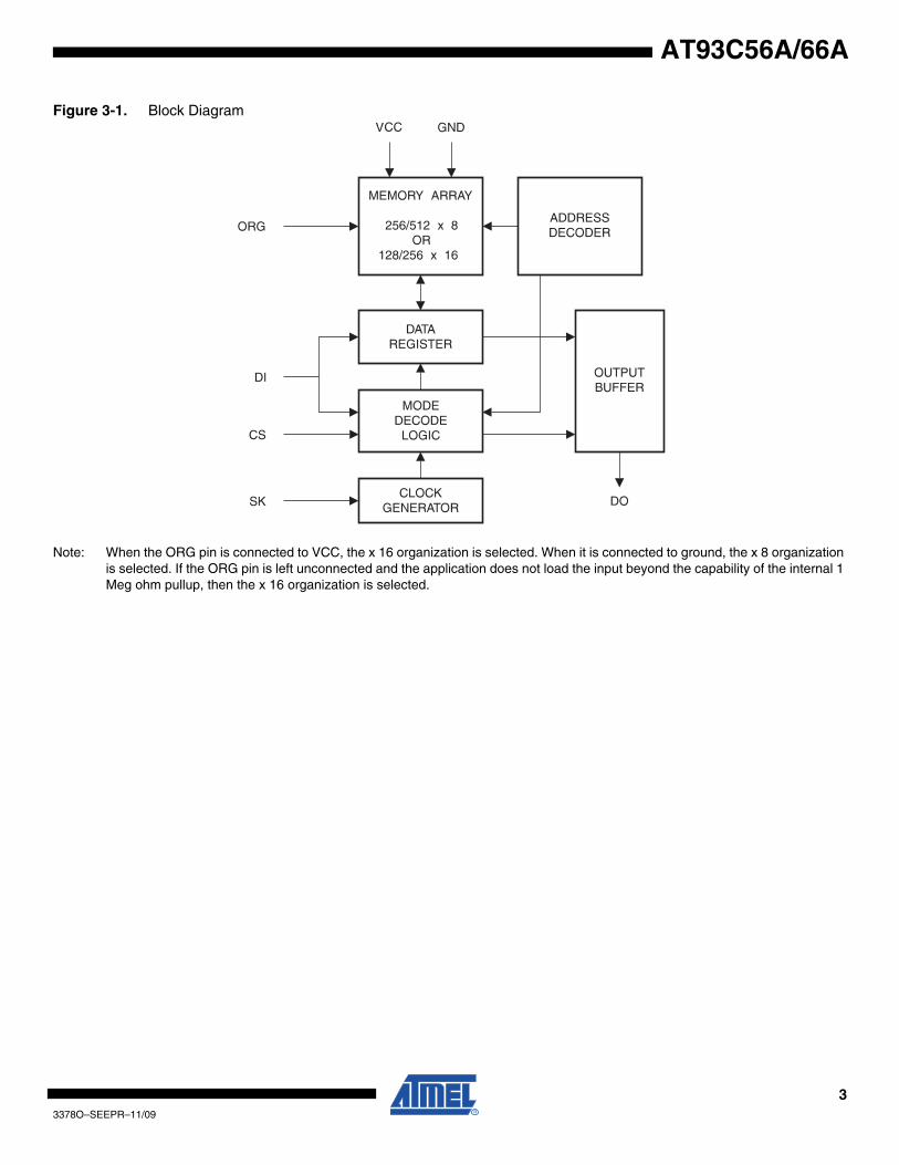
7. AT93C66A Ordering Information(1)
Ordering Code Package Operation Range
AT93C66A-10PU-2.7(2)
AT93C66A-10PU-1.8(2)
AT93C66A-10SU-2.7(2)
AT93C66A-10SU-1.8(2)
AT93C66AW-10SU-2.7(2)
AT93C66AW-10SU-1.8(2)
AT93C66A-10TU-2.7(2)
AT93C66A-10TU-1.8(2)
AT93C66AU3-10UU-1.8(2)
AT93C66AD3-10DH-1.8(3)
AT93C66AY1-10YU-1.8(2) (Not recommended for new design)AT93C66AY6-10YH-1.8(3)
8P38P38S18S18S28S28A28A2
8U3-18D38Y18Y6
Lead-free/Halogen-free/Industrial Temperature
(40C to 85C)
AT93C66A-W1.8-11(4) Die SaleIndustrial Temperature
(40C to 85C)
Package Type
8P3 8-lead, 0.300" Wide, Plastic Dual Inline Package (PDIP)
8S1 8-lead, 0.150" Wide, Plastic Gull Wing Small Outline (JEDEC SOIC)
8S2 8-lead, 0.200" Wide, Plastic Gull Wing Small Outline (EIAJ SOIC)
8A2 8-lead, 0.170" Wide, Thin Shrink Small Outline Package (TSSOP)
8U3-1 8-ball, die Ball Grid Array Package (dBGA2)
8Y1 8-lead, 4.90 mm x 3.00 mm Body, Dual Footprint, Non-leaded, Miniature Array Package (MAP)
8Y6 8-lead, 2.00 mm x 3.00 mm Body, 0.50 mm Pitch, Ultra Thin Mini-MAP, Dual No Lead package (DFN), (MLP 2x3 mm)
8D3 8-lead, 1.80 mm x 2.20 mm Body, Ultra Lead Frame Land Grid Array (ULA)
Options
2.7 Low-voltage (2.7V to 5.5V)
1.8 Low-voltage (1.8V to 5.5V)
133378O–SEEPR–11/09

8. Packaging Information
8.1 8P3 – PDIP
2325 Orchard ParkwaySan Jose, CA 95131
TITLE DRAWING NO.
R
REV. 8P3, 8-lead, 0.300" Wide Body, Plastic Dual In-line Package (PDIP)
01/09/02
8P3 B
D
D1
E
E1
e
Lb2
b
A2 A
1
N
eAc
b34 PLCS
Top View
Side View
End View
COMMON DIMENSIONS(Unit of Measure = inches)
SYMBOL MIN NOM MAX NOTE
Notes: 1. This drawing is for general information only; refer to JEDEC Drawing MS-001, Variation BA for additional information.2. Dimensions A and L are measured with the package seated in JEDEC seating plane Gauge GS-3.3. D, D1 and E1 dimensions do not include mold Flash or protrusions. Mold Flash or protrusions shall not exceed 0.010 inch.4. E and eA measured with the leads constrained to be perpendicular to datum.5. Pointed or rounded lead tips are preferred to ease insertion.6. b2 and b3 maximum dimensions do not include Dambar protrusions. Dambar protrusions shall not exceed 0.010 (0.25 mm).
A 0.210 2
A2 0.115 0.130 0.195
b 0.014 0.018 0.022 5
b2 0.045 0.060 0.070 6
b3 0.030 0.039 0.045 6
c 0.008 0.010 0.014
D 0.355 0.365 0.400 3
D1 0.005 3
E 0.300 0.310 0.325 4
E1 0.240 0.250 0.280 3
e 0.100 BSC
eA 0.300 BSC 4
L 0.115 0.130 0.150 2
143378O–SEEPR–11/09
AT93C56A/66A

AT93C56A/66A
8.2 8S1 – JEDEC SOIC
1150 E. Cheyenne Mtn. Blvd.Colorado Springs, CO 80906
TITLE DRAWING NO.
R
REV.
Note:
10/7/03
8S1, 8-lead (0.150" Wide Body), Plastic Gull Wing Small Outline (JEDEC SOIC)
8S1 B
COMMON DIMENSIONS(Unit of Measure = mm)
SYMBOL MIN NOM MAX NOTE
A1 0.10 – 0.25
These drawings are for general information only. Refer to JEDEC Drawing MS-012, Variation AA for proper dimensions, tolerances, datums, etc.
A 1.35 – 1.75
b 0.31 – 0.51
C 0.17 – 0.25
D 4.80 – 5.00
E1 3.81 – 3.99
E 5.79 – 6.20
e 1.27 BSC
L 0.40 – 1.27
∅ 0˚ – 8˚
∅
Top ViewEnd View
Side View
e B
D
A
A1
N
E
1
C
E1
L
153378O–SEEPR–11/09

8.3 8S2 – EIAJ SOIC
2325 Orchard ParkwaySan Jose, CA 95131
TITLE DRAWING NO.
R
REV. 8S2, 8-lead, 0.209" Body, Plastic Small Outline Package (EIAJ)
10/7/03
8S2 C
COMMON DIMENSIONS(Unit of Measure = mm)
SYMBOL MIN NOM MAX NOTE
Notes: 1. This drawing is for general information only; refer to EIAJ Drawing EDR-7320 for additional information.2. Mismatch of the upper and lower dies and resin burrs are not included.3. It is recommended that upper and lower cavities be equal. If they are different, the larger dimension shall be regarded.4. Determines the true geometric position.5. Values b and C apply to pb/Sn solder plated terminal. The standard thickness of the solder layer shall be 0.010 +0.010/−0.005 mm.
A 1.70 2.16
A1 0.05 0.25
b 0.35 0.48 5
C 0.15 0.35 5
D 5.13 5.35
E1 5.18 5.40 2, 3
E 7.70 8.26
L 0.51 0.85
∅ 0˚ 8˚
e 1.27 BSC 4
End View
Side View
e b
A
A1
D
E
N
1
C
E1
∅
L
Top View
COMMON DIMENSIONS(Unit of Measure = mm)
SYMBOL MIN NOM MAX NOTE
Notes: 1. This drawing is for general information only; refer to EIAJ Drawing EDR-7320 for additional information. 2. Mismatch of the upper and lower dies and resin burrs aren't included. 3. It is recommended that upper and lower cavities be equal. If they are different, the larger dimension shall be regarded. 4. Determines the true geometric position. 5. Values b,C apply to plated terminal. The standard thickness of the plating layer shall measure between 0.007 to .021 mm.
θθ
11
N
E
CC
E1E
A
b
L
A1
e
D
TOP VIEW
END VIEW
SIDE VIEW
A
A1
b
C
D
E1
E
L
θ
e
1.70
0.05
0.35
0.15
5.13
5.18
7.70
0.51
0˚
2.16
0.25
0.48
0.35
5.35
5.40
8.26
0.85
8˚
5
5
2, 3
41.27 BSC
DRAWING NO.2325 Orchard ParkwaySan Jose, CA 95131R
REV.
8S2 D
04/07/06
TITLE8S2, 8-lead, 0.209" Body, Plastic Small Outline Package (EIAJ)
163378O–SEEPR–11/09
AT93C56A/66A

AT93C56A/66A
8.4 8Y6 – MiniMap (MLP 2x3)
TITLE DRAWING NO. GPC REV. Package Drawing Contact: [email protected] 8Y6YNZ E
8Y6, 8-lead 2.0x3.0 mm Body, 0.50 mm Pitch,UltraThin Mini-MAP, Dual No Lead Package(Sawn)(UDFN)
11/21/08
Notes: 1. This drawing is for general information only. Refer to JEDEC Drawing MO-229, for proper dimensions, tolerances, datums, etc.
2. Dimension b applies to metallized terminal and is measured between 0.15 mm and 0.30 mm from the terminal tip. If the terminal has the optional radius on the other end of the terminal, the dimension should not be measured in that radius area.
3. Soldering the large thermal pad is optional, but not recommended. No electrical connection is accomplished to the device through this pad, so if soldered it should be tied to ground
COMMON DIMENSIONS(Unit of Measure = mm)
SYMBOL MIN NOM MAX NOTE
D 2.00 BSC
E 3.00 BSC
D2 1.40 1.50 1.60
E2 - - 1.40
A - - 0.60
A1 0.0 0.02 0.05
A2 - - 0.55
A3 0.20 REF
L 0.20 0.30 0.40
e 0.50 BSC
b 0.20 0.25 0.30 2
A2A2
b(8X)(8X)
Pin 1 IDPin 1 ID
Pin 1Pin 1IndexIndexAreaArea
A1A1
A3A3
D
E
A
L (8X)L (8X)
e (6X)e (6X)
1.50 REF.1.50 REF.
D2D2
E2E2
173378O–SEEPR–11/09

8.5 8Y1 – Map
A – – 0.90
A1 0.00 – 0.05
D 4.70 4.90 5.10
E 2.80 3.00 3.20
D1 0.85 1.00 1.15
E1 0.85 1.00 1.15
b 0.25 0.30 0.35
e 0.65 TYP
L 0.50 0.60 0.70
PIN 1 INDEX AREA
D
E
A
A1 b
8 7 6
e
5
L
D1
E1
PIN 1 INDEX AREA
1 2 3 4
A
Top View End View Bottom View
Side View
2325 Orchard ParkwaySan Jose, CA 95131
TITLE DRAWING NO.
R
REV. 8Y1, 8-lead (4.90 x 3.00 mm Body) MSOP Array Package (MAP) Y1 C8Y1
2/28/03
COMMON DIMENSIONS(Unit of Measure = mm)
SYMBOL MIN NOM MAX NOTE
183378O–SEEPR–11/09
AT93C56A/66A

AT93C56A/66A
8.6 8A2 – TSSOP
2325 Orchard ParkwaySan Jose, CA 95131
TITLE DRAWING NO.
R
REV.
5/30/02
COMMON DIMENSIONS(Unit of Measure = mm)
SYMBOL MIN NOM MAX NOTE
D 2.90 3.00 3.10 2, 5
E 6.40 BSC
E1 4.30 4.40 4.50 3, 5
A – – 1.20
A2 0.80 1.00 1.05
b 0.19 – 0.30 4
e 0.65 BSC
L 0.45 0.60 0.75
L1 1.00 REF
8A2, 8-lead, 4.4 mm Body, Plastic Thin Shrink Small Outline Package (TSSOP)
Notes: 1. This drawing is for general information only. Refer to JEDEC Drawing MO-153, Variation AA, for proper dimensions, tolerances, datums, etc.
2. Dimension D does not include mold Flash, protrusions or gate burrs. Mold Flash, protrusions and gate burrs shall not exceed 0.15 mm (0.006 in) per side.
3. Dimension E1 does not include inter-lead Flash or protrusions. Inter-lead Flash and protrusions shall not exceed 0.25 mm (0.010 in) per side.
4. Dimension b does not include Dambar protrusion. Allowable Dambar protrusion shall be 0.08 mm total in excess of the b dimension at maximum material condition. Dambar cannot be located on the lower radius of the foot. Minimum space between protrusion and adjacent lead is 0.07 mm.
5. Dimension D and E1 to be determined at Datum Plane H.
8A2 B
Side View
End ViewTop View
A2
A
L
L1
D
123
E1
N
b
Pin 1 indicatorthis corner
E
e
193378O–SEEPR–11/09

8.7 8U3-1 – dBGA2
TITLE DRAWING NO.
R
REV.1150E Cheyenne Mt. BlvdColorado Springs, CO 80906 PO8U3-1 b
5/3/05
COMMON DIMENSIONS(Unit of Measure = mm)
SYMBOL MIN NOM MAX NOTE
A 0.713 0.79 0.85
A1 0.09 0.14 0.19
A2 0.40 0.45 0.50
b 0.20 0.25 0.30 2
D 1.50 BSC
E 2.00 BSC
e 0.50 BSC
e1 0.25 REF
d 1.00 BSC
d1 0.25 REF
8U3-1, 8-ball, 1.50 x 2.00 mm Body, 0.50 mm pitch,Small Die Ball Grid Array Package (dBGA2)
bD
E
A
A2
A1
Bottom View8 Solder Balls
Side View
Top View
PIN 1 BALL PAD CORNER
PIN 1 BALL PAD CORNER
1. This drawing is for general information only.2. Dimension ‘b’ is measured at maximum solder ball diameter
4
5
31
e
2
678
d
(e1)
(d1)
1.
203378O–SEEPR–11/09
AT93C56A/66A

AT93C56A/66A
8.8 8D3 - ULA
1150 E. Cheyenne Mtn. Blvd.Colorado Springs, CO 80906
TITLE DRAWING NO.
R
REV. 8D3, 8-lead (1.80 x 2.20 mm Body) Ultra Leadframe Land Grid Array (ULLGA) D3 08D3
11/15/05
COMMON DIMENSIONS(Unit of Measure = mm)
SYMBOL MIN NOM MAX NOTE
A – – 0.40
A1 0.00 – 0.05
D 1.70 1.80 1.90
E 2.10 2.20 2.30
b 0.15 0.20 0.25
e 0.40 TYP
e1 1.20 REF
L 0.25 0.30 0.35
0.10
0.15
b
6 57
43
E
D
8
1 2
PIN #1 ID
TOP VIEW
L
b
A1
Ae
PIN #1 ID
SIDE VIEW BOTTOM VIEW
e1
213378O–SEEPR–11/09

9. Revision History
Revision No. Date Comments
3378O 07/2012 Not recommended for new design. Use AT93C56B/66B.
3378O 11/2009 Added 8S2 package drawing
3378N 1/2009 Updated 8Y6 package drawing
3378M 7/2008 Updated Ordering Codes
3378L 11/2007Updated to new templateAdded ULA package offering
3378K 12/2006
Removed DC/Don’t Connect and replaced with NC/No ConenctAdjusted size of Block diagram on pg. 2Made all diagrams on pages 6-9 consistently the same sizeCorrected 8U3-1
223378O–SEEPR–11/09
AT93C56A/66A

3378O–SEEPR–11/09
Headquarters International
Atmel Corporation2325 Orchard ParkwaySan Jose, CA 95131USATel: 1(408) 441-0311Fax: 1(408) 487-2600
Atmel AsiaRoom 1219Chinachem Golden Plaza77 Mody Road TsimshatsuiEast KowloonHong KongTel: (852) 2721-9778Fax: (852) 2722-1369
Atmel EuropeLe Krebs8, Rue Jean-Pierre TimbaudBP 30978054 Saint-Quentin-en-Yvelines CedexFranceTel: (33) 1-30-60-70-00Fax: (33) 1-30-60-71-11
Atmel Japan9F, Tonetsu Shinkawa Bldg.1-24-8 ShinkawaChuo-ku, Tokyo 104-0033JapanTel: (81) 3-3523-3551Fax: (81) 3-3523-7581
Product Contact
Web Sitewww.atmel.com
Technical [email protected]
Sales Contactwww.atmel.com/contacts
Literature Requestswww.atmel.com/literature
Disclaimer: The information in this document is provided in connection with Atmel products. No license, express or implied, by estoppel or otherwise, to anyintellectual property right is granted by this document or in connection with the sale of Atmel products. EXCEPT AS SET FORTH IN ATMEL’S TERMS AND CONDI-TIONS OF SALE LOCATED ON ATMEL’S WEB SITE, ATMEL ASSUMES NO LIABILITY WHATSOEVER AND DISCLAIMS ANY EXPRESS, IMPLIED OR STATUTORYWARRANTY RELATING TO ITS PRODUCTS INCLUDING, BUT NOT LIMITED TO, THE IMPLIED WARRANTY OF MERCHANTABILITY, FITNESS FOR A PARTICULARPURPOSE, OR NON-INFRINGEMENT. IN NO EVENT SHALL ATMEL BE LIABLE FOR ANY DIRECT, INDIRECT, CONSEQUENTIAL, PUNITIVE, SPECIAL OR INCIDEN-TAL DAMAGES (INCLUDING, WITHOUT LIMITATION, DAMAGES FOR LOSS OF PROFITS, BUSINESS INTERRUPTION, OR LOSS OF INFORMATION) ARISING OUT OFTHE USE OR INABILITY TO USE THIS DOCUMENT, EVEN IF ATMEL HAS BEEN ADVISED OF THE POSSIBILITY OF SUCH DAMAGES. Atmel makes norepresentations or warranties with respect to the accuracy or completeness of the contents of this document and reserves the right to make changes to specificationsand product descriptions at any time without notice. Atmel does not make any commitment to update the information contained herein. Unless specifically providedotherwise, Atmel products are not suitable for, and shall not be used in, automotive applications. Atmel’s products are not intended, authorized, or warranted for useas components in applications intended to support or sustain life.
© 2009 Atmel Corporation. All rights reserved. Atmel®, Atmel logo and combinations thereof, and others, are registered trademarks or trade-marks of Atmel Corporation or its subsidiaries. Other terms and product names may be trademarks of others.


![Atmel AT24C256C · Atmel AT24C256C [DATASHEET] 3 8568E–SEEPR–8/2012 3. Block Diagram 4. Pin Descriptions Serial Clock (SCL): The SCL input is used to positive-edge clock data](https://img.pdfslide.us/doc/110x75/5f05568e7e708231d41278a3/atmel-at24c256c-atmel-at24c256c-datasheet-3-8568easeepra82012-3-block-diagram.jpg)


![Atmel AT24C512C - Digi-Key Sheets/Atmel PDFs...Atmel AT24C512C [DATASHEET] 2 8720C–SEEPR–7/12 1. Pin Configurations and Pinouts Figure 1. Pin Configurations 2. Absolute Maximum](https://img.pdfslide.us/doc/110x75/5b0293b37f8b9a65618f6d93/atmel-at24c512c-digi-key-sheetsatmel-pdfsatmel-at24c512c-datasheet-2-8720cseepr712.jpg)


![Atmel AT24C128C CORPORATION... · Atmel AT24C128C [DATASHEET] 3 8734B–SEEPR–9/2012 3. Block Diagram 4. Pin Descriptions Serial Clock (SCL): The SCL input is used to positive-edge](https://img.pdfslide.us/doc/110x75/5f0556907e708231d41278ab/atmel-corporation-atmel-at24c128c-datasheet-3-8734baseepra92012-3-block.jpg)

![The Sleeping Beauty (suite) [Op.66a ; TH 234]](https://img.pdfslide.us/doc/110x75/61b2488c04d0f3189c584a51/the-sleeping-beauty-suite-op66a-th-234.jpg)