Embed Size (px)
Citation preview
Serial Lite III Streaming Intel FPGAIP Core User Guide
Updated for Intel® Quartus® Prime Design Suite: 18.1.1
SubscribeSend Feedback
UG-01126 | 2019.02.25Latest document on the web: PDF | HTML

Contents
1. Serial Lite III Streaming Intel FPGA IP Core Quick Reference........................................ 4
2. About the Serial Lite III Streaming IP Core.................................................................... 62.1. Serial Lite III Streaming IP Core Protocol..................................................................62.2. Serial Lite III Streaming IP Core Protocol Operating Modes..........................................7
2.2.1. Continuous Mode.......................................................................................72.2.2. Burst Mode............................................................................................... 8
2.3. Performance and Resource Utilization....................................................................... 8
3. Getting Started ............................................................................................................ 123.1. Installing and Licensing Intel FPGA IP Cores............................................................ 123.2. Intel FPGA IP Evaluation Mode...............................................................................13
3.2.1. Intel FPGA IP Evaluation Mode Timeout Behavior..........................................153.3. Specifying IP Core Parameters and Options............................................................. 15
3.3.1. Serial Lite III Streaming IP Core Parameter Editor........................................ 163.3.2. Intel Arria 10 Designs...............................................................................16
3.4. Serial Lite III Streaming IP Core Parameters............................................................173.4.1. Parameter Settings for Intel Stratix 10 Devices............................................ 173.4.2. Parameter Settings for Intel Arria 10 Devices...............................................193.4.3. Parameter Settings for Stratix V and Arria V GZ Devices................................21
3.5. Transceiver Reconfiguration Controller for Stratix V and Arria V GZ Designs................. 223.6. IP Core Generation Output (Intel Quartus Prime Pro Edition)......................................223.7. IP Core Generation Output (Intel Quartus Prime Standard Edition)............................. 253.8. Simulating.......................................................................................................... 26
3.8.1. Simulating Intel FPGA IP Cores.................................................................. 263.8.2. Simulation Parameters..............................................................................263.8.3. Simulating and Verifying the Design........................................................... 28
4. Serial Lite III Streaming IP Core Design Examples....................................................... 304.1. Serial Lite III Streaming IP Core Design Example for Intel Stratix 10 Devices...............304.2. Serial Lite III Streaming IP Core Design Example for Intel Arria 10 Devices................. 304.3. Serial Lite III Streaming IP Design Examples for Stratix V Devices..............................30
5. Serial Lite III Streaming IP Core Functional Description...............................................315.1. IP Core Architecture............................................................................................. 31
5.1.1. Serial Lite III Streaming Source Core..........................................................325.1.2. Serial Lite III Streaming Sink Core............................................................. 355.1.3. Serial Lite III Streaming IP Core Duplex Core.............................................. 375.1.4. Interlaken PHY IP Duplex Core or Native PHY IP Duplex Core - Interlaken
Mode or PCS Gearbox Mode.......................................................................375.1.5. Intel Stratix 10, Intel Arria 10, Stratix V, and Arria V GZ Variations................ 38
5.2. Transmission Overheads and Lane Rate Calculations................................................. 395.3. Reset................................................................................................................. 405.4. Link-Up Sequence................................................................................................ 415.5. Error Detection, Reporting, and Recovering Mechanism............................................. 445.6. CRC-32 Error Injection ........................................................................................ 495.7. FIFO ECC Protection ............................................................................................ 495.8. User Data Interface Waveforms............................................................................. 49
Contents
Serial Lite III Streaming Intel FPGA IP Core User Guide Send Feedback
2
5.9. Signals...............................................................................................................525.9.1. Signals for Intel Stratix 10 Devices.............................................................525.9.2. Signals for Intel Arria 10 Devices............................................................... 605.9.3. Signals for Stratix V and Arria V GZ Devices................................................ 67
5.10. Accessing Configuration and Status Registers.........................................................74
6. Serial Lite III Streaming IP Core Clocking Guidelines................................................... 756.1. Standard Clocking Mode....................................................................................... 75
6.1.1. Standard Clocking Mode in Serial Lite III Streaming Intel FPGA IP Core(Intel Stratix 10 Devices)..........................................................................75
6.1.2. Standard Clocking Mode in Intel Arria 10, Stratix V, and Arria V Devices .........796.2. Advanced Clocking Mode.......................................................................................82
6.2.1. Advanced Clocking Mode Structure for Serial Lite III Streaming Intel FPGAIP Core (Intel Stratix 10 Devices)...............................................................82
6.2.2. Advanced Clocking Mode Structure For Intel Arria 10, Stratix V, and ArriaV Devices................................................................................................85
6.3. Standard Clocking Mode vs Advanced Clocking Mode................................................ 886.4. Clocking Implementation Guidelines....................................................................... 89
6.4.1. Choosing TX PLL Type...............................................................................916.5. Core Latency.......................................................................................................93
7. Serial Lite III Streaming IP Core Configuration and Status Registers........................... 957.1. Register Map.......................................................................................................957.2. Configuration and Status Registers.........................................................................95
8. Serial Lite III Streaming IP Core Debugging Guidelines............................................. 1028.1. Creating a Signal Tap Debug File to Match Your Design Hierarchy .............................1028.2. Serial Lite III Streaming IP Core Link Debugging.................................................... 103
8.2.1. Source Core Link Debugging ...................................................................1038.2.2. Sink Core Link Debugging ...................................................................... 104
9. Serial Lite III Streaming IP Core User Guide Archives................................................ 106
10. Document Revision History for the Intel FPGA Serial Lite III Streaming IP CoreUser Guide.............................................................................................................107
Contents
Send Feedback Serial Lite III Streaming Intel FPGA IP Core User Guide
3

1. Serial Lite III Streaming Intel FPGA IP CoreQuick Reference
The Serial Lite III Streaming Intel® FPGA IP core is a lightweight protocol suitable forhigh bandwidth streaming data in chip-to-chip, board-to-board, and backplaneapplications.
Table 1. Serial Lite III Streaming IP Core
Item Description
ReleaseInformation
Version 18.1.1 Intel Quartus® Prime Pro Edition (Intel Stratix® 10 and Intel Arria® 10devices)18.1 Intel Quartus Prime Standard Edition (Intel Arria 10, Stratix V and Arria V GZdevices)
Release Date December 2018 (Intel Quartus Prime Pro Edition v18.1.1)September 2018 (Intel Quartus Prime Standard Edition v18.1)
IP CatalogName
• Serial Lite III Streaming Intel FPGA IP (Intel Stratix 10, Stratix V, and Arria V GZdevices)
• Serial Lite III Streaming Intel Arria 10 FPGA IP
Ordering Code IP-SLITE3/ST
Product ID 010A
Vendor ID 6AF7
IP CoreInformation
Core Features • Up to 28 Gbps(1) lane data rate for Intel Stratix 10 with H-tile or E-tiletransceivers.
• Up to 17.4 Gbps lane data rates for Intel Arria 10 devices.• Supports 1–24 serial lanes in configurations that provide nominal bandwidths
from 3.125 gigabits per second (Gbps) to over 400 Gbps.
ProtocolFeatures
• Source (simplex transmitter), sink (simplex receiver), and duplex operations• Support for single or multiple lanes• 64/67B physical layer encoding• Payload and idle scrambling• Error detection• Low overhead framing• Low point-to-point transfer latency
TypicalApplication
• High resolution video• Radar processing• Medical imaging• Baseband processing in wireless infrastructure
Device FamilySupport
Intel Stratix 10 (Advance support), Intel Arria 10 (Final support) , Arria V GZ (Finalsupport), and Stratix V (Final support) FPGA devices.
continued...
(1) Refer to Table 2 on page 8, Table 4 on page 9, and Table 5 on page 10 for maximumlane supported per data rate.
UG-01126 | 2019.02.25
Send Feedback
Intel Corporation. All rights reserved. Intel, the Intel logo, Altera, Arria, Cyclone, Enpirion, MAX, Nios, Quartusand Stratix words and logos are trademarks of Intel Corporation or its subsidiaries in the U.S. and/or othercountries. Intel warrants performance of its FPGA and semiconductor products to current specifications inaccordance with Intel's standard warranty, but reserves the right to make changes to any products and servicesat any time without notice. Intel assumes no responsibility or liability arising out of the application or use of anyinformation, product, or service described herein except as expressly agreed to in writing by Intel. Intelcustomers are advised to obtain the latest version of device specifications before relying on any publishedinformation and before placing orders for products or services.*Other names and brands may be claimed as the property of others.
ISO9001:2015Registered

Item Description
Advance support - The IP core is available for simulation and compilation for thisdevice family. FPGA programming file (.pof) support is not available for QuartusPrime Pro – Stratix 10 Edition Beta software and as such IP timing closure cannot beguaranteed. Timing models include initial engineering estimates of delays based onearly post-layout information. The timing models are subject to change as silicontesting improves the correlation between the actual silicon and the timing models.You can use this IP core for system architecture and resource utilization studies,simulation, pinout, system latency assessments, basic timing assessments (pipelinebudgeting), and I/O transfer strategy (data-path width, burst depth, I/O standardstradeoffs).Final support - The IP core is verified with final timing models for this devicefamily. The IP core meets all the functional and timing requirements for the devicefamily and can be used in production designs.
Design Tools • IP parameter editor in the Intel Quartus Prime software for IP designinstantiation and compilation
• Timing Analyzer in the Intel Quartus Prime software for timing analysis• ModelSim-Intel FPGA Edition, MATLAB, or third-party tool using NativeLink for
design simulation or synthesis
Related Information
• Intel Software Installation and Licensing
• What's New in Intel IP
• Serial Lite III Streaming Intel FPGA IP Core Release Notes
• Errata for Intel FPGA Serial Lite III Streaming IP core in the Knowledge Base
• Serial Lite III Streaming IP Core User Guide Archives on page 106Provides a list of user guides for previous versions of the Intel FPGA Serial LiteIII Streaming IP core.
• Timing and Power ModelsReports the default device support levels in the current version of the QuartusPrime Pro Edition software.
• Timing and Power ModelsReports the default device support levels in the current version of the QuartusPrime Standard Edition software.
• Intel FPGA Serial Lite III Streaming IP Core Design Example User Guide for IntelStratix 10 Devices
• Intel Arria 10 Serial Lite III Streaming IP Core Design Example User Guide
1. Serial Lite III Streaming Intel FPGA IP Core Quick Reference
UG-01126 | 2019.02.25
Send Feedback Serial Lite III Streaming Intel FPGA IP Core User Guide
5
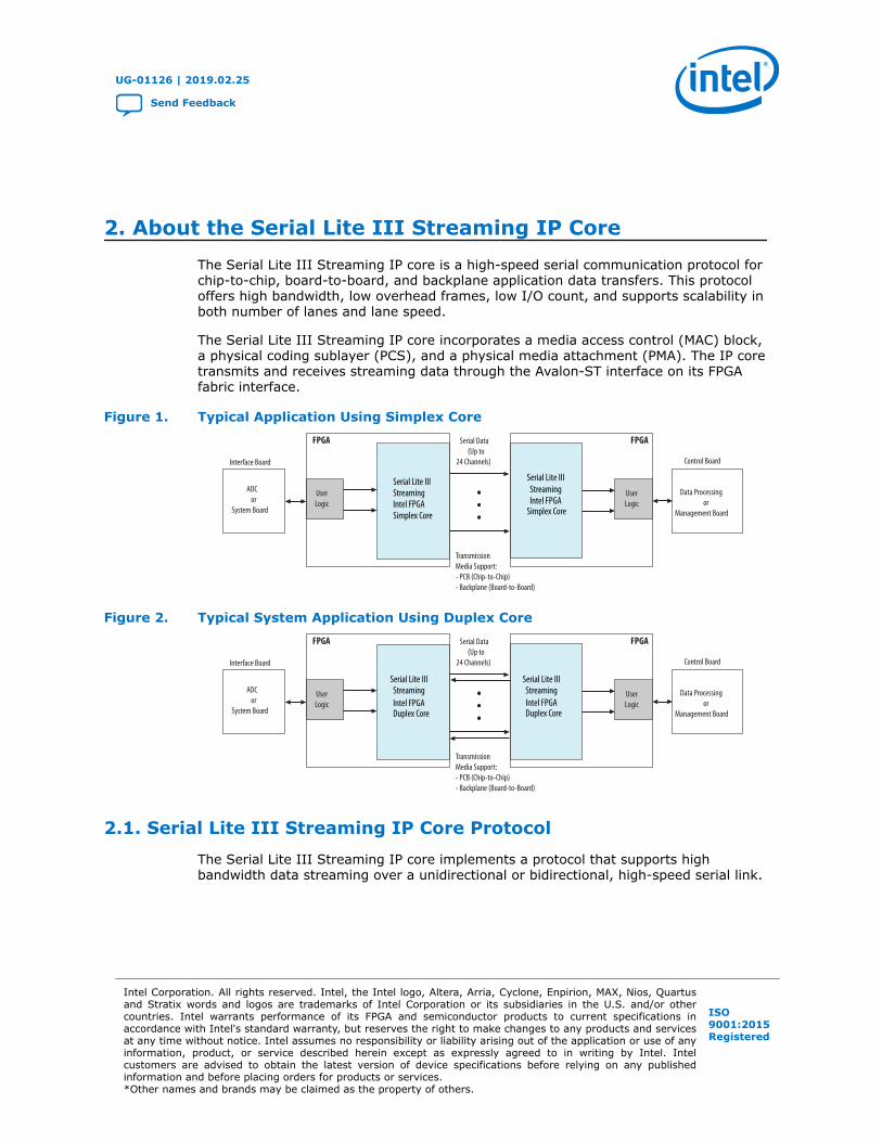
2. About the Serial Lite III Streaming IP CoreThe Serial Lite III Streaming IP core is a high-speed serial communication protocol forchip-to-chip, board-to-board, and backplane application data transfers. This protocoloffers high bandwidth, low overhead frames, low I/O count, and supports scalability inboth number of lanes and lane speed.
The Serial Lite III Streaming IP core incorporates a media access control (MAC) block,a physical coding sublayer (PCS), and a physical media attachment (PMA). The IP coretransmits and receives streaming data through the Avalon-ST interface on its FPGAfabric interface.
Figure 1. Typical Application Using Simplex Core
Serial Lite IIIStreaming
Serial Lite IIIStreaming
FPGA FPGA
UserLogic
UserLogic
Serial Data(Up to
24 Channels)
TransmissionMedia Support:- PCB (Chip-to-Chip)- Backplane (Board-to-Board)
Data Processingor
Management Board
ADCor
System Board
Control BoardInterface Board
Intel FPGA Intel FPGA
Simplex Core Simplex Core
Figure 2. Typical System Application Using Duplex Core
Serial Lite IIIStreaming
Serial Lite IIIStreaming
FPGA FPGA
UserLogic
UserLogic
Serial Data(Up to
24 Channels)
TransmissionMedia Support:- PCB (Chip-to-Chip)- Backplane (Board-to-Board)
Data Processingor
Management Board
ADCor
System Board
Control BoardInterface Board
Intel FPGA Intel FPGADuplex Core Duplex Core
2.1. Serial Lite III Streaming IP Core Protocol
The Serial Lite III Streaming IP core implements a protocol that supports highbandwidth data streaming over a unidirectional or bidirectional, high-speed serial link.
UG-01126 | 2019.02.25
Send Feedback
Intel Corporation. All rights reserved. Intel, the Intel logo, Altera, Arria, Cyclone, Enpirion, MAX, Nios, Quartusand Stratix words and logos are trademarks of Intel Corporation or its subsidiaries in the U.S. and/or othercountries. Intel warrants performance of its FPGA and semiconductor products to current specifications inaccordance with Intel's standard warranty, but reserves the right to make changes to any products and servicesat any time without notice. Intel assumes no responsibility or liability arising out of the application or use of anyinformation, product, or service described herein except as expressly agreed to in writing by Intel. Intelcustomers are advised to obtain the latest version of device specifications before relying on any publishedinformation and before placing orders for products or services.*Other names and brands may be claimed as the property of others.
ISO9001:2015Registered

The Serial Lite III Streaming IP core has the following protocol features:
• Simplex source only, simplex sink only, and duplex (transmitter and receiver)operations
• Support for single or multiple lanes
• 64B/67B physical layer encoding
• Payload and idle scrambling
• Error detection:
— Source burst gap mismatch error
— Error Correction Code (ECC) with 1 bit correction and 2 or more bits detection
— Sink and source adaptation First In First Out (FIFO) overflow error
— Sink Cyclic Redundancy Check (CRC) errors
— Sink Physical Coding Sublayer (PCS) synchronization, metaframe, or CRCerrors
• Low protocol overhead
• Low point-to-point transfer latency
• Reduces soft logic resource utilization using hardened Transceiver Native PHY IntelArria 10 FPGA IP core and L-Tile/H-Tile/E-Tile Transceiver Intel Stratix 10 FPGA IPCore or Interlaken PHY v18.1 IP core (Stratix V and Arria V GZ devices)
2.2. Serial Lite III Streaming IP Core Protocol Operating Modes
The protocol defines two operating modes for different applications: continuous andburst mode.
The IP core that you generate can be in either mode. No parameter option is availableto select between continuous and burst modes. The selection depends on how youprovide data at the Avalon-ST TX interface.
2.2.1. Continuous Mode
The Serial Lite III Streaming link operating in continuous mode accepts and transmitsuser data over the link, and presents it at the user interface at the receiving link atthe same rate and without gaps in the stream, if user logic does not de-assert datavalid signal as part of the stream. However, if user logic de-asserts the data validsignal in the middle of data transfer, the streaming interface will no longer operate incontinuous mode and there is no guarantee that the end-point sink is able to replicatethe exact data pattern of the source. When operating in this mode, a linkimplementing the protocol looks like a data pipe that can transparently forward alldata presented on the user interface to the far end of the link.
Continuous mode is appropriate for applications that require a simple interface totransmit a single, high bandwidth data stream. An example of this application issensor data links for radar and wireless infrastructure. With this mode, dataconverters can connect to either end of the link with minimal interface logic.
Important: Continuous mode is applicable only in Standard Clocking Mode., It is not possible tooperate in this mode with asynchronous clocking implementation becauseasynchronous clocking requires data valid signal to be de-asserted, to break the datastream to avoid FIFO overflow at the sink due to PPM difference.
2. About the Serial Lite III Streaming IP Core
UG-01126 | 2019.02.25
Send Feedback Serial Lite III Streaming Intel FPGA IP Core User Guide
7

2.2.2. Burst Mode
The Serial Lite III Streaming IP core link operating in burst mode accepts bursts ofdata across the user interface and transmits each burst across the link as a discretedata burst.
Burst mode is appropriate for applications where the data stream is divided into burstsof data. An example of this application is uncompressed digital video where the datastream is divided into lines of display raster. This mode provides more flexibility to theclocking and also supports multiplexing of multiple data streams across the link.
Important: The minimum required gap between bursts is 1 user clock cycle on the transmit side.Therefore, you must provide one extra user clock cycle between an end of burst andthe start of the next burst. The Serial Lite III Streaming IP core allows you to selectbetween 1 or 2 burst gap. To connect the IP core of version 15.1 to IP core of theprevious version, you must select a burst gap of 2 for backward compatibility.
Related Information
• Standard Clocking Mode on page 75
• Advanced Clocking Mode on page 82
2.3. Performance and Resource Utilization
Serial Lite III Streaming Intel FPGA IP in Intel Stratix 10 devices support the followingtransceiver tiles for each device speed grade and data rate:
Table 2. Serial Lite III Streaming Intel FPGA IP Transceiver Tiles Support in IntelStratix 10 Devices
Data Rate Core Speed Grade Maximum Supported Lanes
L-Tile Transceiver H-Tile Transceiver E-Tile Transceiver
17.4 Gbps 1 24 24 24
2 22 24 24
3 18 20 24
25.0 Gbps 1 6 8 12
2 4 6 8
28.0 Gbps 1 N/A 4 4
2 N/A 2 1
Table 3. Serial Lite III Streaming IP Performance and Resource Utilization with L-TileTransceiver in Intel Stratix 10 DevicesThese typical resources and expected performance for different Serial Lite III Streaming IP core variants areobtained using the Intel Quartus Prime Pro Edition software targeting the Intel Stratix 10 1SG280LU3F50E1VGdevice for 17.4 Gbps data rate and 1SG280LU2F50E1VG device for 25 Gbps data rate. The resource utilizationnumbers are the same for ECC enabled and disabled.
Direction Clocking Mode Data Lanes Per-Lane DataRate (Mbps)
ALMs Primary Secondary M20K
Source Standard 24 17400 11675 13622 776 49
Standard 6 25000 3160 3644 215 13
continued...
2. About the Serial Lite III Streaming IP Core
UG-01126 | 2019.02.25
Serial Lite III Streaming Intel FPGA IP Core User Guide Send Feedback
8
Direction Clocking Mode Data Lanes Per-Lane DataRate (Mbps)
ALMs Primary Secondary M20K
Advance 24 17400 11691 13571 919 49
Advance 6 25000 3139 3687 181 13
Sink Standard 24 17400 5181 7532 2065 49
Standard 6 25000 1463 2009 513 13
Advance 24 17400 4485 6994 2359 0
Advance 6 25000 1245 1792 629 0
Duplex Standard 24 17400 15793 19074 2913 98
Standard 6 25000 4299 5123 698 26
Advance 24 17400 14984 18880 2976 49
Advance 6 25000 4025 4980 812 13
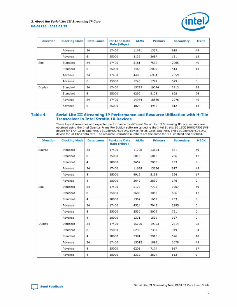
Table 4. Serial Lite III Streaming IP Performance and Resource Utilization with H-TileTransceiver in Intel Stratix 10 DevicesThese typical resources and expected performance for different Serial Lite III Streaming IP core variants areobtained using the Intel Quartus Prime Pro Edition software targeting the Intel Stratix 10 1SG280HU3F50E1VGdevice for 17.4 Gbps data rate, 1SG280HU2F50E1VG device for 25 Gbps data rate, and 1SG280HU1F50E1VGdevice for 28 Gbps data rate. The resource utilization numbers are the same for ECC enabled and disabled.
Direction Clocking Mode Data Lanes Per-Lane DataRate (Mbps)
ALMs Primary Secondary M20K
Source Standard 24 17400 11708 13604 851 49
Standard 8 25000 5013 5048 296 17
Standard 4 28000 2652 2803 193 9
Advance 24 17400 11638 13636 817 49
Advance 8 25000 4919 5195 324 17
Advance 4 28000 2649 2830 176 9
Sink Standard 24 17400 5175 7732 1907 49
Standard 8 25000 2685 3063 666 17
Standard 4 28000 1367 1659 263 9
Advance 24 17400 4524 7045 2295 0
Advance 8 25000 2530 3009 761 0
Advance 4 28000 1371 1599 397 0
Duplex Standard 24 17400 15790 19353 2814 98
Standard 8 25000 6239 7332 949 34
Standard 4 28000 3391 3916 526 18
Advance 24 17400 15012 18941 3078 49
Advance 8 25000 6208 7174 987 17
Advance 4 28000 3312 3824 533 9
2. About the Serial Lite III Streaming IP Core
UG-01126 | 2019.02.25
Send Feedback Serial Lite III Streaming Intel FPGA IP Core User Guide
9
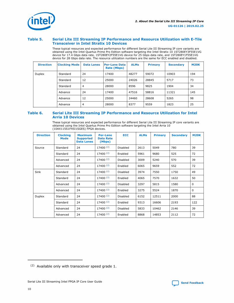
Table 5. Serial Lite III Streaming IP Performance and Resource Utilization with E-TileTransceiver in Intel Stratix 10 DevicesThese typical resources and expected performance for different Serial Lite III Streaming IP core variants areobtained using the Intel Quartus Prime Pro Edition software targeting the Intel Stratix 10 1ST280EY3F55E1VGdevice for 17.4 Gbps data rate, 1ST280EY2F55E1VG device for 25 Gbps data rate, and 1ST280EY1F55E1VGdevice for 28 Gbps data rate. The resource utilization numbers are the same for ECC enabled and disabled.
Direction Clocking Mode Data Lanes Per-Lane DataRate (Mbps)
ALMs Primary Secondary M20K
Duplex Standard 24 17400 48277 59072 10903 194
Standard 12 25000 24026 28845 5717 73
Standard 4 28000 8596 9825 1904 34
Advance 24 17400 47516 58816 11321 145
Advance 12 25000 24460 28608 5265 98
Advance 4 28000 8377 9559 1823 25
Table 6. Serial Lite III Streaming IP Performance and Resource Utilization for IntelArria 10 DevicesThese typical resources and expected performance for different Serial Lite III Streaming IP core variants areobtained using the Intel Quartus Prime Pro Edition software targeting the Intel Arria 10(10AX115S1F45I1SGES) FPGA devices.
Direction ClockingMode
MaximumSupportedData Lanes
Per-LaneData Rate
(Mbps)
ECC ALMs Primary Secondary M20K
Source Standard 24 17400 (2) Disabled 2613 5049 780 39
Standard 24 17400 (2) Enabled 5961 9680 525 72
Advanced 24 17400 (2) Disabled 3009 5240 570 39
Advanced 24 17400 (2) Enabled 6065 9659 552 72
Sink Standard 24 17400 (2) Disabled 3974 7550 1750 49
Standard 24 17400 (2) Enabled 4065 7570 1632 50
Advanced 24 17400 (2) Disabled 3297 5815 1580 0
Advanced 24 17400 (2) Enabled 3275 5524 1870 0
Duplex Standard 24 17400 (2) Disabled 6152 12511 2000 88
Standard 24 17400 (2) Enabled 9313 16606 2193 122
Advanced 24 17400 (2) Disabled 5833 10462 2146 39
Advanced 24 17400 (2) Enabled 8868 14853 2112 72
(2) Available only with transceiver speed grade 1.
2. About the Serial Lite III Streaming IP Core
UG-01126 | 2019.02.25
Serial Lite III Streaming Intel FPGA IP Core User Guide Send Feedback
10
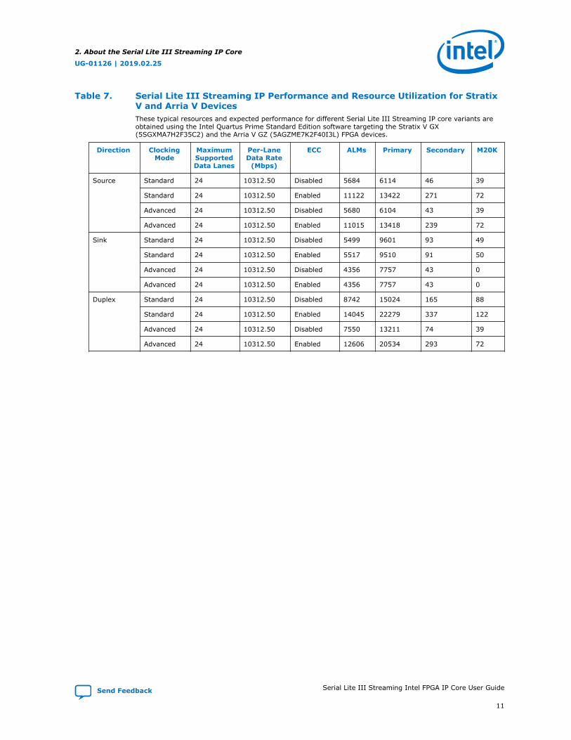
Table 7. Serial Lite III Streaming IP Performance and Resource Utilization for StratixV and Arria V DevicesThese typical resources and expected performance for different Serial Lite III Streaming IP core variants areobtained using the Intel Quartus Prime Standard Edition software targeting the Stratix V GX(5SGXMA7H2F35C2) and the Arria V GZ (5AGZME7K2F40I3L) FPGA devices.
Direction ClockingMode
MaximumSupportedData Lanes
Per-LaneData Rate
(Mbps)
ECC ALMs Primary Secondary M20K
Source Standard 24 10312.50 Disabled 5684 6114 46 39
Standard 24 10312.50 Enabled 11122 13422 271 72
Advanced 24 10312.50 Disabled 5680 6104 43 39
Advanced 24 10312.50 Enabled 11015 13418 239 72
Sink Standard 24 10312.50 Disabled 5499 9601 93 49
Standard 24 10312.50 Enabled 5517 9510 91 50
Advanced 24 10312.50 Disabled 4356 7757 43 0
Advanced 24 10312.50 Enabled 4356 7757 43 0
Duplex Standard 24 10312.50 Disabled 8742 15024 165 88
Standard 24 10312.50 Enabled 14045 22279 337 122
Advanced 24 10312.50 Disabled 7550 13211 74 39
Advanced 24 10312.50 Enabled 12606 20534 293 72
2. About the Serial Lite III Streaming IP Core
UG-01126 | 2019.02.25
Send Feedback Serial Lite III Streaming Intel FPGA IP Core User Guide
11
3. Getting StartedRelated Information
• Introduction to Intel IP CoresProvides general information about all Intel FPGA IP cores, includingparameterizing, generating, upgrading, and simulating IP cores.
• Creating Version-Independent IP and Qsys Simulation ScriptsCreate simulation scripts that do not require manual updates for software or IPversion upgrades.
• Project Management Best PracticesGuidelines for efficient management and portability of your project and IP files.
3.1. Installing and Licensing Intel FPGA IP Cores
The Intel Quartus Prime software installation includes the Intel FPGA IP library. Thislibrary provides many useful IP cores for your production use without the need for anadditional license. Some Intel FPGA IP cores require purchase of a separate license forproduction use. The Intel FPGA IP Evaluation Mode allows you to evaluate theselicensed Intel FPGA IP cores in simulation and hardware, before deciding to purchase afull production IP core license. You only need to purchase a full production license forlicensed Intel IP cores after you complete hardware testing and are ready to use theIP in production.
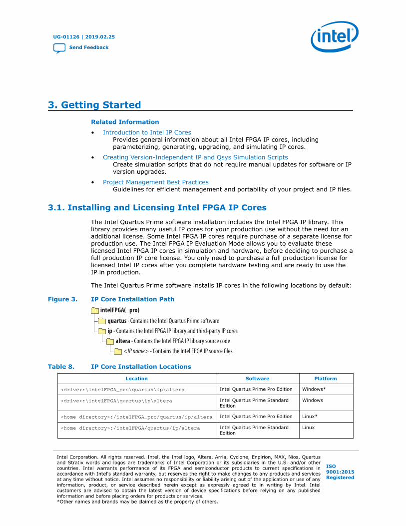
The Intel Quartus Prime software installs IP cores in the following locations by default:
Figure 3. IP Core Installation Path
intelFPGA(_pro)
quartus - Contains the Intel Quartus Prime softwareip - Contains the Intel FPGA IP library and third-party IP cores
altera - Contains the Intel FPGA IP library source code<IP name> - Contains the Intel FPGA IP source files
Table 8. IP Core Installation Locations
Location Software Platform
<drive>:\intelFPGA_pro\quartus\ip\altera Intel Quartus Prime Pro Edition Windows*
<drive>:\intelFPGA\quartus\ip\altera Intel Quartus Prime StandardEdition
Windows
<home directory>:/intelFPGA_pro/quartus/ip/altera Intel Quartus Prime Pro Edition Linux*
<home directory>:/intelFPGA/quartus/ip/altera Intel Quartus Prime StandardEdition
Linux
UG-01126 | 2019.02.25
Send Feedback
Intel Corporation. All rights reserved. Intel, the Intel logo, Altera, Arria, Cyclone, Enpirion, MAX, Nios, Quartusand Stratix words and logos are trademarks of Intel Corporation or its subsidiaries in the U.S. and/or othercountries. Intel warrants performance of its FPGA and semiconductor products to current specifications inaccordance with Intel's standard warranty, but reserves the right to make changes to any products and servicesat any time without notice. Intel assumes no responsibility or liability arising out of the application or use of anyinformation, product, or service described herein except as expressly agreed to in writing by Intel. Intelcustomers are advised to obtain the latest version of device specifications before relying on any publishedinformation and before placing orders for products or services.*Other names and brands may be claimed as the property of others.
ISO9001:2015Registered

Note: The Intel Quartus Prime software does not support spaces in the installation path.
3.2. Intel FPGA IP Evaluation Mode
The free Intel FPGA IP Evaluation Mode allows you to evaluate licensed Intel FPGA IPcores in simulation and hardware before purchase. Intel FPGA IP Evaluation Modesupports the following evaluations without additional license:
• Simulate the behavior of a licensed Intel FPGA IP core in your system.
• Verify the functionality, size, and speed of the IP core quickly and easily.
• Generate time-limited device programming files for designs that include IP cores.
• Program a device with your IP core and verify your design in hardware.
Intel FPGA IP Evaluation Mode supports the following operation modes:
• Tethered—Allows running the design containing the licensed Intel FPGA IPindefinitely with a connection between your board and the host computer.Tethered mode requires a serial joint test action group (JTAG) cable connectedbetween the JTAG port on your board and the host computer, which is running theIntel Quartus Prime Programmer for the duration of the hardware evaluationperiod. The Programmer only requires a minimum installation of the Intel QuartusPrime software, and requires no Intel Quartus Prime license. The host computercontrols the evaluation time by sending a periodic signal to the device via theJTAG port. If all licensed IP cores in the design support tethered mode, theevaluation time runs until any IP core evaluation expires. If all of the IP coressupport unlimited evaluation time, the device does not time-out.
• Untethered—Allows running the design containing the licensed IP for a limitedtime. The IP core reverts to untethered mode if the device disconnects from thehost computer running the Intel Quartus Prime software. The IP core also revertsto untethered mode if any other licensed IP core in the design does not supporttethered mode.
When the evaluation time expires for any licensed Intel FPGA IP in the design, thedesign stops functioning. All IP cores that use the Intel FPGA IP Evaluation Mode timeout simultaneously when any IP core in the design times out. When the evaluationtime expires, you must reprogram the FPGA device before continuing hardwareverification. To extend use of the IP core for production, purchase a full productionlicense for the IP core.
You must purchase the license and generate a full production license key before youcan generate an unrestricted device programming file. During Intel FPGA IP EvaluationMode, the Compiler only generates a time-limited device programming file (<projectname>_time_limited.sof) that expires at the time limit.
3. Getting Started
UG-01126 | 2019.02.25
Send Feedback Serial Lite III Streaming Intel FPGA IP Core User Guide
13

Figure 4. Intel FPGA IP Evaluation Mode Flow
Install the Intel Quartus Prime Software with Intel FPGA IP Library
Parameterize and Instantiate aLicensed Intel FPGA IP Core
Purchase a Full Production IP License
Verify the IP in a Supported Simulator
Compile the Design in theIntel Quartus Prime Software
Generate a Time-Limited DeviceProgramming File
Program the Intel FPGA Deviceand Verify Operation on the Board
No
Yes
IP Ready forProduction Use?
Include Licensed IP in Commercial Products
Note: Refer to each IP core's user guide for parameterization steps and implementationdetails.
Intel licenses IP cores on a per-seat, perpetual basis. The license fee includes first-year maintenance and support. You must renew the maintenance contract to receiveupdates, bug fixes, and technical support beyond the first year. You must purchase afull production license for Intel FPGA IP cores that require a production license, beforegenerating programming files that you may use for an unlimited time. During IntelFPGA IP Evaluation Mode, the Compiler only generates a time-limited deviceprogramming file (<project name>_time_limited.sof) that expires at the timelimit. To obtain your production license keys, visit the Self-Service Licensing Center.
The Intel FPGA Software License Agreements govern the installation and use oflicensed IP cores, the Intel Quartus Prime design software, and all unlicensed IP cores.
3. Getting Started
UG-01126 | 2019.02.25
Serial Lite III Streaming Intel FPGA IP Core User Guide Send Feedback
14

Related Information
• Intel Quartus Prime Licensing Site
• Introduction to Intel FPGA Software Installation and Licensing
3.2.1. Intel FPGA IP Evaluation Mode Timeout Behavior
All IP cores in a device time out simultaneously when the most restrictive evaluationtime is reached. If there is more than one IP core in a design, the time-out behavior ofthe other IP cores may mask the time-out behavior of a specific IP core .
For IP cores, the untethered time-out is one hour; the tethered time-out value isindefinite. Your design stops working after the hardware evaluation time expires. TheIntel Quartus Prime software uses Intel FPGA IP Evaluation Mode Files (.ocp) in yourproject directory to identify your use of the Intel FPGA IP Evaluation Mode evaluationprogram. After you activate the feature, do not delete these files.
When the evaluation time expires, the link_up signal goes low.
Related Information
AN 320: Using Intel FPGA IP Evaluation Mode
3.3. Specifying IP Core Parameters and Options
Follow these steps to specify IP core parameters and options.
1. In the Platform Designer IP Catalog (Tools ➤ IP Catalog), locate and double-click the name of the IP core to customize. The parameter editor appears.
2. Specify a top-level name for your custom IP variation. This name identifies the IPcore variation files in your project. If prompted, also specify the target FPGAdevice family and output file HDL preference. Click OK.
3. Specify parameters and options for your IP variation:
• Optionally select preset parameter values. Presets specify all initial parametervalues for specific applications (where provided).
• Specify parameters defining the IP core functionality, port configurations, anddevice-specific features.
• Specify options for generation of a timing netlist, simulation model, testbench,or example design (where applicable).
• Specify options for processing the IP core files in other EDA tools.
4. Click Finish to generate synthesis and other optional files matching your IPvariation specifications. The parameter editor generates the top-level .qsys IPvariation file and HDL files for synthesis and simulation. Some IP cores alsosimultaneously generate a testbench or example design for hardware testing.
The top-level IP variation is added to the current Intel Quartus Prime project. ClickProject ➤ Add/Remove Files in Project to manually add a .qsys (Intel QuartusPrime Standard Edition) or .ip (Intel Quartus Prime Pro Edition) file to a project.Make appropriate pin assignments to connect ports.
3. Getting Started
UG-01126 | 2019.02.25
Send Feedback Serial Lite III Streaming Intel FPGA IP Core User Guide
15
3.3.1. Serial Lite III Streaming IP Core Parameter Editor
Based on the values you set, the Serial Lite III Streaming IP core parameter editorautomatically calculates the rest of the parameters, and provides you with thefollowing values or information:
• Input data rate per lane
• Transceiver data rate per lane
• A list of feasible transceiver reference clock frequencies, one of which you select toprovide to the core
Important: If your design targets Stratix V or Arria V GZ devices, you cannot migrate your designto Intel Arria 10 and Intel Stratix 10 devices automatically. For Intel Arria 10 devices,the transceiver reconfiguration functionality is embedded inside the transceivers.Therefore, you must re-instantiate the IP core to target Intel Arria 10 devices. ForIntel Stratix 10 devices, you must re-instantiate the IP core to target specifictransceiver tiles due to the transceiver architecture differences. You cannot migrateyour design from Intel Stratix 10 L-tile/H-Tile devices to Intel Stratix 10 E-Tile devices.
Related Information
Parameter Settings for Intel Stratix 10 Devices on page 17
3.3.2. Intel Arria 10 Designs
If your design targets the Intel Arria 10 devices:
• The parameter editor displays a message about the required output clockfrequency of the external TX PLL IP clock. For source or duplex modes, connectthe Transceiver PHY Reset Controller to the TX PLL to ensure the appropriate HSSIpower-up sequence.
• For source only Intel Arria 10 implementations, the parameter editor does notprovide the transceiver reference clock frequency because the user is expected toprovide the transmit serial clock. If you use an on-chip PLL to generate thetransmit serial clock, you can use the same PLL reference clock frequency that youprovide to the core in the sink direction, operating at the same user clockfrequency (or equivalent transceiver lane data rate).
• The Serial Lite III Streaming Intel Arria 10 FPGA IP core expects the user toprovide the transmitter's serial clock. If you compile the IP without the properserial clock, the Intel Quartus Prime Compiler issues a compilation error.
• When generating the example testbench, the Serial Lite III Streaming Intel Arria10 FPGA IP core instantiates an external transceiver ATX PLL for the transmitserial clock based on the required user clock only when configured in sink orduplex mode. The transceiver ATX PLL core is configured with the transceiverreference clock specified in the parameter editor and transmit serial clock.
• To generate the Serial Lite III Streaming Intel Arria 10 FPGA IP Core exampletestbench using the parameter editor, select Generate Example Designs ><directory_name>. Intel recommends that you generate the Intel Arria 10simulation testbench for the sink or duplex direction.
Related Information
• Parameter Settings for Intel Arria 10 Devices on page 19
• Intel Stratix 10, Intel Arria 10, Stratix V, and Arria V GZ Variations on page 38
3. Getting Started
UG-01126 | 2019.02.25
Serial Lite III Streaming Intel FPGA IP Core User Guide Send Feedback
16
• Intel Arria 10 SerialLite III Streaming IP Core Design Example User Guide
3.4. Serial Lite III Streaming IP Core Parameters
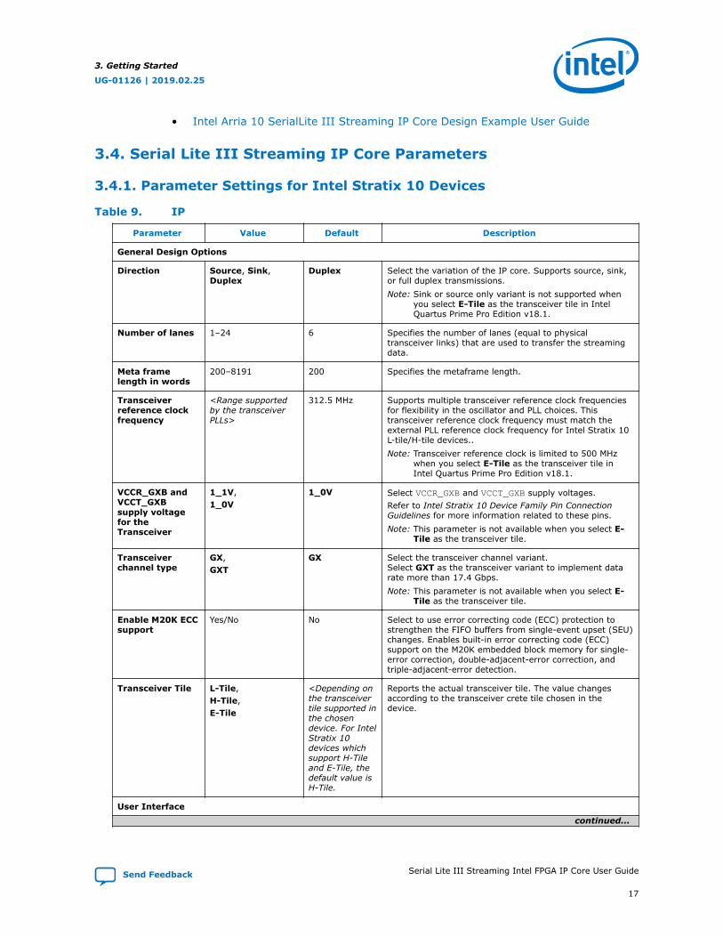
3.4.1. Parameter Settings for Intel Stratix 10 Devices
Table 9. IP
Parameter Value Default Description
General Design Options
Direction Source, Sink,Duplex
Duplex Select the variation of the IP core. Supports source, sink,or full duplex transmissions.Note: Sink or source only variant is not supported when
you select E-Tile as the transceiver tile in IntelQuartus Prime Pro Edition v18.1.
Number of lanes 1–24 6 Specifies the number of lanes (equal to physicaltransceiver links) that are used to transfer the streamingdata.
Meta framelength in words
200–8191 200 Specifies the metaframe length.
Transceiverreference clockfrequency
<Range supportedby the transceiverPLLs>
312.5 MHz Supports multiple transceiver reference clock frequenciesfor flexibility in the oscillator and PLL choices. Thistransceiver reference clock frequency must match theexternal PLL reference clock frequency for Intel Stratix 10L-tile/H-tile devices..Note: Transceiver reference clock is limited to 500 MHz
when you select E-Tile as the transceiver tile inIntel Quartus Prime Pro Edition v18.1.
VCCR_GXB andVCCT_GXBsupply voltagefor theTransceiver
1_1V,1_0V
1_0V Select VCCR_GXB and VCCT_GXB supply voltages.Refer to Intel Stratix 10 Device Family Pin ConnectionGuidelines for more information related to these pins.Note: This parameter is not available when you select E-
Tile as the transceiver tile.
Transceiverchannel type
GX,GXT
GX Select the transceiver channel variant.Select GXT as the transceiver variant to implement datarate more than 17.4 Gbps.Note: This parameter is not available when you select E-
Tile as the transceiver tile.
Enable M20K ECCsupport
Yes/No No Select to use error correcting code (ECC) protection tostrengthen the FIFO buffers from single-event upset (SEU)changes. Enables built-in error correcting code (ECC)support on the M20K embedded block memory for single-error correction, double-adjacent-error correction, andtriple-adjacent-error detection.
Transceiver Tile L-Tile,H-Tile,E-Tile
<Depending onthe transceivertile supported inthe chosendevice. For IntelStratix 10devices whichsupport H-Tileand E-Tile, thedefault value isH-Tile.
Reports the actual transceiver tile. The value changesaccording to the transceiver crete tile chosen in thedevice.
User Interfacecontinued...
3. Getting Started
UG-01126 | 2019.02.25
Send Feedback Serial Lite III Streaming Intel FPGA IP Core User Guide
17
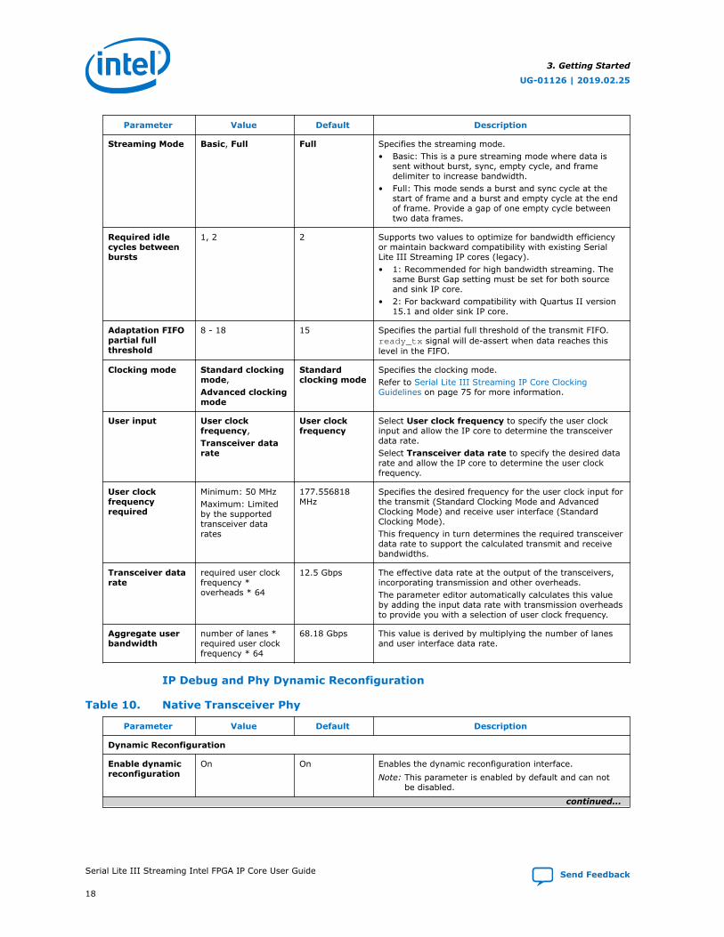
Parameter Value Default Description
Streaming Mode Basic, Full Full Specifies the streaming mode.• Basic: This is a pure streaming mode where data is
sent without burst, sync, empty cycle, and framedelimiter to increase bandwidth.
• Full: This mode sends a burst and sync cycle at thestart of frame and a burst and empty cycle at the endof frame. Provide a gap of one empty cycle betweentwo data frames.
Required idlecycles betweenbursts
1, 2 2 Supports two values to optimize for bandwidth efficiencyor maintain backward compatibility with existing SerialLite III Streaming IP cores (legacy).• 1: Recommended for high bandwidth streaming. The
same Burst Gap setting must be set for both sourceand sink IP core.
• 2: For backward compatibility with Quartus II version15.1 and older sink IP core.
Adaptation FIFOpartial fullthreshold
8 - 18 15 Specifies the partial full threshold of the transmit FIFO.ready_tx signal will de-assert when data reaches thislevel in the FIFO.
Clocking mode Standard clockingmode,Advanced clockingmode
Standardclocking mode
Specifies the clocking mode.Refer to Serial Lite III Streaming IP Core ClockingGuidelines on page 75 for more information.
User input User clockfrequency,Transceiver datarate
User clockfrequency
Select User clock frequency to specify the user clockinput and allow the IP core to determine the transceiverdata rate.Select Transceiver data rate to specify the desired datarate and allow the IP core to determine the user clockfrequency.
User clockfrequencyrequired
Minimum: 50 MHzMaximum: Limitedby the supportedtransceiver datarates
177.556818MHz
Specifies the desired frequency for the user clock input forthe transmit (Standard Clocking Mode and AdvancedClocking Mode) and receive user interface (StandardClocking Mode).This frequency in turn determines the required transceiverdata rate to support the calculated transmit and receivebandwidths.
Transceiver datarate
required user clockfrequency *overheads * 64
12.5 Gbps The effective data rate at the output of the transceivers,incorporating transmission and other overheads.The parameter editor automatically calculates this valueby adding the input data rate with transmission overheadsto provide you with a selection of user clock frequency.
Aggregate userbandwidth
number of lanes *required user clockfrequency * 64
68.18 Gbps This value is derived by multiplying the number of lanesand user interface data rate.
IP Debug and Phy Dynamic Reconfiguration
Table 10. Native Transceiver Phy
Parameter Value Default Description
Dynamic Reconfiguration
Enable dynamicreconfiguration
On On Enables the dynamic reconfiguration interface.Note: This parameter is enabled by default and can not
be disabled.
continued...
3. Getting Started
UG-01126 | 2019.02.25
Serial Lite III Streaming Intel FPGA IP Core User Guide Send Feedback
18

Parameter Value Default Description
Enable AlteraDebug MasterEndpoint
On/Off Off Enables ADME and Optional Reconfiguration Logicparameters of the L-Tile/H-Tile/E-Tile Transceiver NativePHY Intel Stratix 10 FPGA IP Core.
Optional Reconfiguration Logic
Enable capabilityregisters
On/Off Off Enables capability registers that provide high levelinformation about the configuration f the transceiverchannel.
Set user-definedIP identifier
User-defined 0 Sets a user-defined numeric identifier that can be readfrom the user_identifier offset when the capabilityregisters are enabled.Note: To set the value, enabled the Enable capability
registers parameter.
Enable controland statusregisters
On/Off Off Enables soft registers to read status signals and writecontrol signals on the PHY interface through theembedded debug.
Enable PRBS(Pseudo RandomBinary Sequence)softaccumulators
On/Off Off Enables soft logic for performing PRBS bit and erroraccumulation when the hard PRBS generator and checkerare used.Note: This parameter is not available when you select E-
Tile as the transceiver tile.
For information about parameters in the PMA Adaptation tab, please refer to thePMA Adaptation topic in the Intel Stratix 10 E-Tile Transceiver PHY User Guide.
Note: The PMA Adaptation tab is only available in Intel Stratix 10 with E-tile transceiverdevices. You must select E-Tile as the Transceiver Tile to use the parameters in thePMA Adaptation tab.
Related Information
• Serial Lite III Streaming IP Core Parameter Editor on page 16
• Intel Stratix 10 L- and H-Tile Transceiver PHY User Guide - DynamicReconfiguration Parameters
• Intel Stratix 10 E-Tile Transceiver PHY User GuideFor more information about the Intel Stratix 10 E-Tile Native PHY IP core.
• Intel Stratix 10 E-Tile Transceiver PHY User GuideFor more information about PMA Adaptation parameters.
3.4.2. Parameter Settings for Intel Arria 10 Devices
Table 11. IP
Parameter Value Default Description
General Design Options
Direction Source, Sink, Duplex Duplex Supports source, sink, or full duplex transmissions.
Number of lanes 1–24 2 Specifies the number of lanes (equal to physicaltransceiver links) that are used to transfer the streamingdata.
continued...
3. Getting Started
UG-01126 | 2019.02.25
Send Feedback Serial Lite III Streaming Intel FPGA IP Core User Guide
19

Parameter Value Default Description
Transceiverreference clockfrequency
<Range supportedby the transceiverPLLs>
644.53125 MHz Supports multiple transceiver reference clock frequenciesfor flexibility in the oscillator and PLL choices. Thistransceiver reference clock frequency must match theexternal PLL reference clock frequency.
Meta framelength in words
200–8191 200 Specifies the metaframe length.
EnableTransceiverNative PHY ADME
On/Off Off Turn on to enable ADME and Optional ReconfigurationLogic parameters of the Transceiver Native PHY Intel Arria10/Intel Cyclone® 10 GX FPGA IP core.
Enable M20K ECCsupport
On/Off Off Turn on to use error correcting code (ECC) protection tostrengthen the FIFO buffers from single-event upset (SEU)changes. Enables built-in error correcting code (ECC)support on the M20K embedded block memory for single-error correction, double-adjacent-error correction, andtriple-adjacent-error detection.
User Interface
Required idlecycles betweenbursts
1, 2 2 Supports two values to optimize for bandwidth efficiencyor maintain backward compatibility with existing SerialLite III Streaming IP cores (legacy).• 1: Recommended for high bandwidth streaming. The
same Burst Gap setting must be set for both sourceand sink IP core.
• 2: For backward compatibility with Quartus II version15.1 and older sink IP core.
Clocking mode Standard clockingmode, Advancedclocking mode
Standardclocking mode
Specifies the clocking mode.Refer to Serial Lite III Streaming IP Core ClockingGuidelines on page 75 for more information.
User input User clockfrequency,Transceiver data rate
User clockfrequency
Select User clock frequency to specify the user clockinput and allow the IP core to determine the transceiverdata rate.Select Transceiver data rate to specify the desired datarate and allow the IP core to determine the user clockfrequency.
User clockfrequencyrequired
Minimum: 50 MHzMaximum: Limitedby the supportedtransceiver datarates
150 MHz Specifies the desired frequency for the user clock input forthe transmit (Standard Clocking Mode and AdvancedClocking Mode) and receive user interface (StandardClocking Mode).This frequency in turn determines the required transceiverdata rate to support the calculated transmit and receivebandwidths.
User clockfrequency output
Minimum: 50 MHzMaximum: Limitedby the supportedtransceiver datarates
150 MHz Specifies the actual user clock frequency as produced bythe fPLL or I/O PLL and is ideally the same as the requiredclock frequency. In certain very high precision situationswhere the desired user clock is provided up to higherdecimal places, this value can vary slightly due to the fPLLor I/O PLL constraints. Change the required clockfrequency to correct the issue if the minute variation isintolerable.
Transceiver datarate
required user clockfrequency *overheads * 64
10.312499Gbps
The effective data rate at the output of the transceivers,incorporating transmission and other overheads.The parameter editor automatically calculates this valueby adding the input data rate with transmission overheadsto provide you with a selection of user clock frequency.
Aggregate userbandwidth
number of lanes *required user clockfrequency * 64
18.75 Gbps This value is derived by multiplying the number of lanesand user interface data rate.
3. Getting Started
UG-01126 | 2019.02.25
Serial Lite III Streaming Intel FPGA IP Core User Guide Send Feedback
20
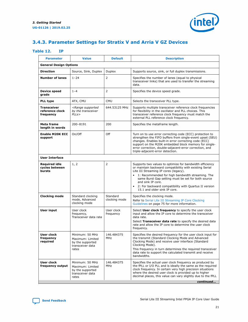
3.4.3. Parameter Settings for Stratix V and Arria V GZ Devices
Table 12. IP
Parameter Value Default Description
General Design Options
Direction Source, Sink, Duplex Duplex Supports source, sink, or full duplex transmissions.
Number of lanes 1–24 2 Specifies the number of lanes (equal to physicaltransceiver links) that are used to transfer the streamingdata.
Device speedgrade
1–4 2 Specifies the device speed grade.
PLL type ATX, CMU CMU Selects the transceiver PLL type.
Transceiverreference clockfrequency
<Range supportedby the transceiverPLLs>
644.53125 MHz Supports multiple transceiver reference clock frequenciesfor flexibility in the oscillator and PLL choices. Thistransceiver reference clock frequency must match theexternal PLL reference clock frequency.
Meta framelength in words
200–8191 200 Specifies the metaframe length.
Enable M20K ECCsupport
On/Off Off Turn on to use error correcting code (ECC) protection tostrengthen the FIFO buffers from single-event upset (SEU)changes. Enables built-in error correcting code (ECC)support on the M20K embedded block memory for single-error correction, double-adjacent-error correction, andtriple-adjacent-error detection.
User Interface
Required idlecycles betweenbursts
1, 2 2 Supports two values to optimize for bandwidth efficiencyor maintain backward compatibility with existing SerialLite III Streaming IP cores (legacy).• 1: Recommended for high bandwidth streaming. The
same Burst Gap setting must be set for both sourceand sink IP core.
• 2: For backward compatibility with Quartus II version15.1 and older sink IP core.
Clocking mode Standard clockingmode, Advancedclocking mode
Standardclocking mode
Specifies the clocking mode.Refer to Serial Lite III Streaming IP Core ClockingGuidelines on page 75 for more information.
User input User clockfrequency,Transceiver data rate
User clockfrequency
Select User clock frequency to specify the user clockinput and allow the IP core to determine the transceiverdata rate.Select Transceiver data rate to specify the desired datarate and allow the IP core to determine the user clockfrequency.
User clockfrequencyrequired
Minimum: 50 MHzMaximum: Limitedby the supportedtransceiver datarates
146.484375MHz
Specifies the desired frequency for the user clock input forthe transmit (Standard Clocking Mode and AdvancedClocking Mode) and receive user interface (StandardClocking Mode).This frequency in turn determines the required transceiverdata rate to support the calculated transmit and receivebandwidths.
User clockfrequency output
Minimum: 50 MHzMaximum: Limitedby the supportedtransceiver datarates
146.484375MHz
Specifies the actual user clock frequency as produced bythe fPLL or I/O PLL and is ideally the same as the requiredclock frequency. In certain very high precision situationswhere the desired user clock is provided up to higherdecimal places, this value can vary slightly due to the fPLL
continued...
3. Getting Started
UG-01126 | 2019.02.25
Send Feedback Serial Lite III Streaming Intel FPGA IP Core User Guide
21
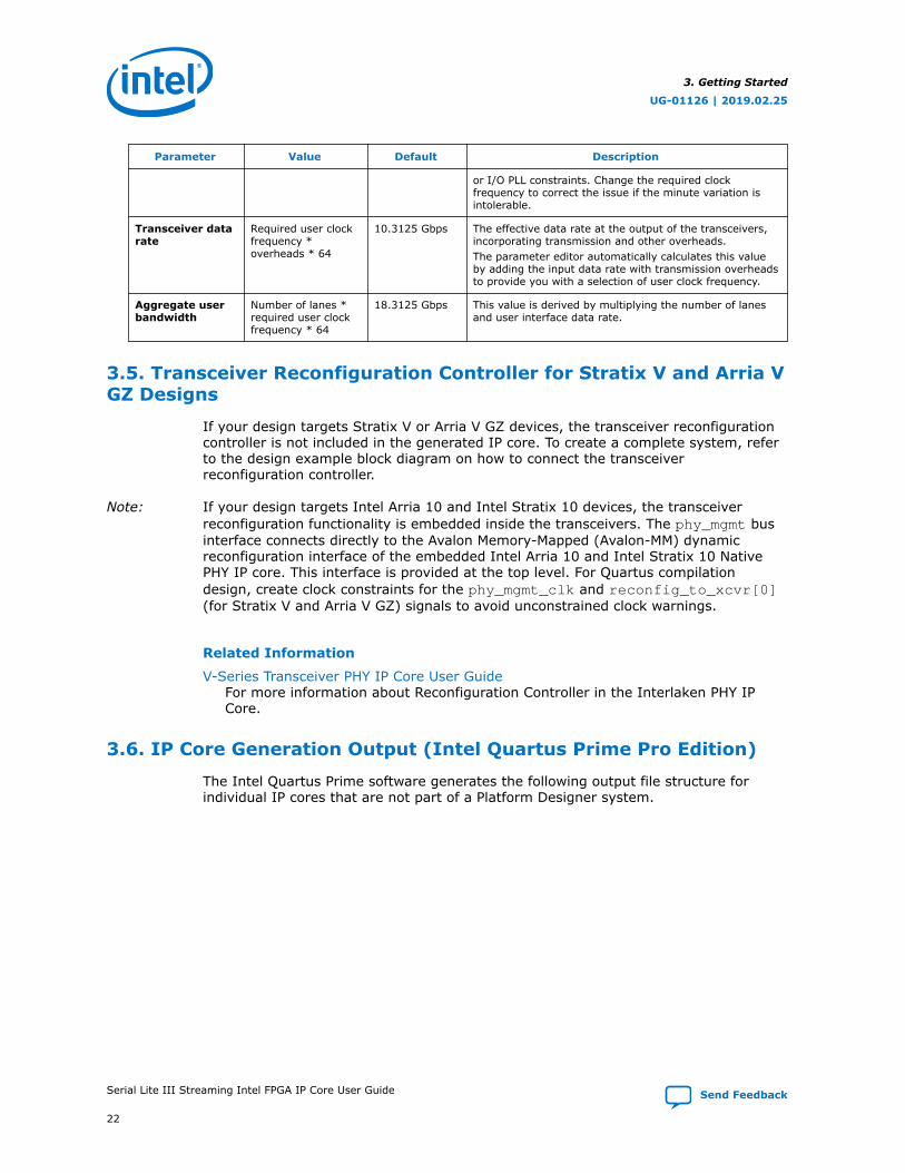
Parameter Value Default Description
or I/O PLL constraints. Change the required clockfrequency to correct the issue if the minute variation isintolerable.
Transceiver datarate
Required user clockfrequency *overheads * 64
10.3125 Gbps The effective data rate at the output of the transceivers,incorporating transmission and other overheads.The parameter editor automatically calculates this valueby adding the input data rate with transmission overheadsto provide you with a selection of user clock frequency.
Aggregate userbandwidth
Number of lanes *required user clockfrequency * 64
18.3125 Gbps This value is derived by multiplying the number of lanesand user interface data rate.
3.5. Transceiver Reconfiguration Controller for Stratix V and Arria VGZ Designs
If your design targets Stratix V or Arria V GZ devices, the transceiver reconfigurationcontroller is not included in the generated IP core. To create a complete system, referto the design example block diagram on how to connect the transceiverreconfiguration controller.
Note: If your design targets Intel Arria 10 and Intel Stratix 10 devices, the transceiverreconfiguration functionality is embedded inside the transceivers. The phy_mgmt businterface connects directly to the Avalon Memory-Mapped (Avalon-MM) dynamicreconfiguration interface of the embedded Intel Arria 10 and Intel Stratix 10 NativePHY IP core. This interface is provided at the top level. For Quartus compilationdesign, create clock constraints for the phy_mgmt_clk and reconfig_to_xcvr[0](for Stratix V and Arria V GZ) signals to avoid unconstrained clock warnings.
Related Information
V-Series Transceiver PHY IP Core User GuideFor more information about Reconfiguration Controller in the Interlaken PHY IPCore.
3.6. IP Core Generation Output (Intel Quartus Prime Pro Edition)
The Intel Quartus Prime software generates the following output file structure forindividual IP cores that are not part of a Platform Designer system.
3. Getting Started
UG-01126 | 2019.02.25
Serial Lite III Streaming Intel FPGA IP Core User Guide Send Feedback
22

Figure 5. Individual IP Core Generation Output (Intel Quartus Prime Pro Edition)
<Project Directory>
<your_ip>_inst.v or .vhd - Lists file for IP core synthesis
<your_ip>.qip - Lists files for IP core synthesis
synth - IP synthesis files
<IP Submodule>_<version> - IP Submodule Library
sim
<your_ip>.v or .vhd - Top-level IP synthesis file
sim - IP simulation files
<simulator vendor> - Simulator setup scripts<simulator_setup_scripts>
<your_ip> - IP core variation files
<your_ip>.ip - Top-level IP variation file
<your_ip>_generation.rpt - IP generation report
<your_ip>.bsf - Block symbol schematic file
<your_ip>.ppf - XML I/O pin information file
<your_ip>.spd - Simulation startup scripts
*
<your_ip>.cmp - VHDL component declaration
<your_ip>.v or vhd - Top-level simulation file
synth
- IP submodule 1 simulation files
- IP submodule 1 synthesis files
<your_ip>_bb.v - Verilog HDL black box EDA synthesis file
<HDL files>
<HDL files>
<your_ip>_tb - IP testbench system *
<your_testbench>_tb.qsys - testbench system file<your_ip>_tb - IP testbench files
your_testbench> _tb.csv or .spd - testbench file
sim - IP testbench simulation files * If supported and enabled for your IP core variation.
<your_ip>.qgsimc - Simulation caching file (Platform Designer)
<your_ip>.qgsynthc - Synthesis caching file (Platform Designer)
Table 13. Output Files of Intel FPGA IP Generation
File Name Description
<your_ip>.ip Top-level IP variation file that contains the parameterization of an IP core inyour project. If the IP variation is part of a Platform Designer system, theparameter editor also generates a .qsys file.
<your_ip>.cmp The VHDL Component Declaration (.cmp) file is a text file that contains localgeneric and port definitions that you use in VHDL design files.
<your_ip>_generation.rpt IP or Platform Designer generation log file. Displays a summary of themessages during IP generation.
continued...
3. Getting Started
UG-01126 | 2019.02.25
Send Feedback Serial Lite III Streaming Intel FPGA IP Core User Guide
23
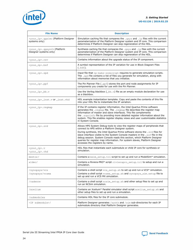
File Name Description
<your_ip>.qgsimc (Platform Designersystems only)
Simulation caching file that compares the .qsys and .ip files with the currentparameterization of the Platform Designer system and IP core. This comparisondetermines if Platform Designer can skip regeneration of the HDL.
<your_ip>.qgsynth (PlatformDesigner systems only)
Synthesis caching file that compares the .qsys and .ip files with the currentparameterization of the Platform Designer system and IP core. This comparisondetermines if Platform Designer can skip regeneration of the HDL.
<your_ip>.csv Contains information about the upgrade status of the IP component.
<your_ip>.bsf A symbol representation of the IP variation for use in Block Diagram Files(.bdf).
<your_ip>.spd Input file that ip-make-simscript requires to generate simulation scripts.The .spd file contains a list of files you generate for simulation, along withinformation about memories that you initialize.
<your_ip>.ppf The Pin Planner File (.ppf) stores the port and node assignments for IPcomponents you create for use with the Pin Planner.
<your_ip>_bb.v Use the Verilog blackbox (_bb.v) file as an empty module declaration for useas a blackbox.
<your_ip>_inst.v or _inst.vhd HDL example instantiation template. Copy and paste the contents of this fileinto your HDL file to instantiate the IP variation.
<your_ip>.regmap If the IP contains register information, the Intel Quartus Prime softwaregenerates the .regmap file. The .regmap file describes the register mapinformation of master and slave interfaces. This file complementsthe .sopcinfo file by providing more detailed register information about thesystem. This file enables register display views and user customizable statisticsin System Console.
<your_ip>.svd Allows HPS System Debug tools to view the register maps of peripherals thatconnect to HPS within a Platform Designer system.During synthesis, the Intel Quartus Prime software stores the .svd files forslave interface visible to the System Console masters in the .sof file in thedebug session. System Console reads this section, which Platform Designerqueries for register map information. For system slaves, Platform Designeraccesses the registers by name.
<your_ip>.v
<your_ip>.vhd
HDL files that instantiate each submodule or child IP core for synthesis orsimulation.
mentor/ Contains a msim_setup.tcl script to set up and run a ModelSim* simulation.
aldec/ Contains a Riviera-PRO* script rivierapro_setup.tcl to setup and run asimulation.
/synopsys/vcs
/synopsys/vcsmx
Contains a shell script vcs_setup.sh to set up and run a VCS* simulation.Contains a shell script vcsmx_setup.sh and synopsys_sim.setup file toset up and run a VCS MX simulation.
/cadence Contains a shell script ncsim_setup.sh and other setup files to set up andrun an NCSim simulation.
/xcelium Contains an Xcelium* Parallel simulator shell script xcelium_setup.sh andother setup files to set up and run a simulation.
/submodules Contains HDL files for the IP core submodule.
<IP submodule>/ Platform Designer generates /synth and /sim sub-directories for each IPsubmodule directory that Platform Designer generates.
3. Getting Started
UG-01126 | 2019.02.25
Serial Lite III Streaming Intel FPGA IP Core User Guide Send Feedback
24
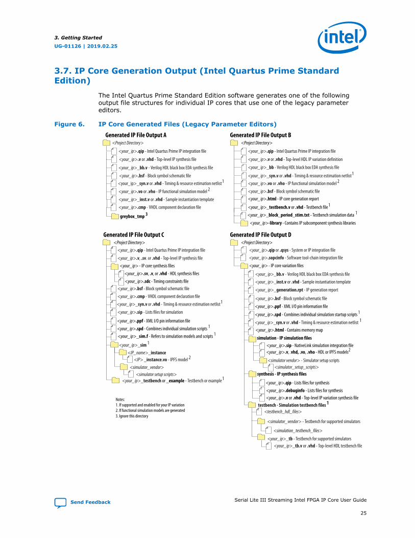
3.7. IP Core Generation Output (Intel Quartus Prime StandardEdition)
The Intel Quartus Prime Standard Edition software generates one of the followingoutput file structures for individual IP cores that use one of the legacy parametereditors.
Figure 6. IP Core Generated Files (Legacy Parameter Editors)
Generated IP File Output B <Project Directory>
<your_ip>.html - IP core generation report
<your_ip>_testbench.v or .vhd - Testbench file1
<your_ip>.bsf - Block symbol schematic file
<your_ip>_syn.v or .vhd - Timing & resource estimation netlist1
<your_ip>_bb - Verilog HDL black box EDA synthesis file
<your_ip>.vo or .vho - IP functional simulation model 2
<your_ip>.qip - Intel Quartus Prime IP integration file
<your_ip>.v or .vhd - Top-level HDL IP variation definition
<your_ip>_block_period_stim.txt - Testbench simulation data 1
<your_ip>-library - Contains IP subcomponent synthesis libraries
Generated IP File Output A <Project Directory>
<your_ip>.v or .vhd - Top-level IP synthesis file
<your_ip>_inst.v or .vhd - Sample instantiation template
<your_ip>.bsf - Block symbol schematic file
<your_ip>.vo or .vho - IP functional simulation model 2<your_ip>_syn.v or .vhd - Timing & resource estimation netlist1
<your_ip>_bb.v - Verilog HDL black box EDA synthesis file
<your_ip>.qip - Intel Quartus Prime IP integration file
greybox_tmp 3
<your_ip>.cmp - VHDL component declaration file
Generated IP File Output C <Project Directory>
<your_ip>_sim 1
<IP> _instance.vo - IPFS model 2
<simulator_vendor><simulator setup scripts>
<your_ip>.qip - Intel Quartus Prime IP integration file
<your_ip>.sip - Lists files for simulation
<your_ip>_testbench or _example - Testbench or example1
<your_ip>.v, .sv. or .vhd - Top-level IP synthesis file
<IP_name>_instance
<your_ip>_syn.v or .vhd - Timing & resource estimation netlist1<your_ip>.cmp - VHDL component declaration file
<your_ip>.bsf - Block symbol schematic file
<your_ip> - IP core synthesis files
<your_ip>.sv, .v, or .vhd - HDL synthesis files
<your_ip>.sdc - Timing constraints file
<your_ip>.ppf - XML I/O pin information file
<your_ip>.spd - Combines individual simulation scripts 1
<your_ip>_sim.f - Refers to simulation models and scripts 1
Notes:1. If supported and enabled for your IP variation2. If functional simulation models are generated3. Ignore this directory
Generated IP File Output D <Project Directory>
<your_ip>_bb.v - Verilog HDL black box EDA synthesis file
<your_ip>_inst.v or .vhd - Sample instantiation template
synthesis - IP synthesis files
<your_ip>.qip - Lists files for synthesis
testbench - Simulation testbench files 1
<testbench_hdl_files>
<simulator_vendor> - Testbench for supported simulators
<simulation_testbench_files>
<your_ip>.v or .vhd - Top-level IP variation synthesis file
simulation - IP simulation files<your_ip>.sip - NativeLink simulation integration file
<simulator vendor> - Simulator setup scripts<simulator_setup_scripts>
<your_ip> - IP core variation files
<your_ip>.qip or .qsys - System or IP integration file
<your_ip>_generation.rpt - IP generation report
<your_ip>.bsf - Block symbol schematic file
<your_ip>.ppf - XML I/O pin information file
<your_ip>.spd - Combines individual simulation startup scripts 1
<your_ip>.html - Contains memory map
<your_ip>.sopcinfo - Software tool-chain integration file
<your_ip>_syn.v or .vhd - Timing & resource estimation netlist 1
<your_ip>.debuginfo - Lists files for synthesis
<your_ip>.v, .vhd, .vo, .vho - HDL or IPFS models2
<your_ip>_tb - Testbench for supported simulators<your_ip>_tb.v or .vhd - Top-level HDL testbench file
3. Getting Started
UG-01126 | 2019.02.25
Send Feedback Serial Lite III Streaming Intel FPGA IP Core User Guide
25
3.8. Simulating
3.8.1. Simulating Intel FPGA IP Cores
The Intel Quartus Prime software supports IP core RTL simulation in specific EDAsimulators. IP generation creates simulation files, including the functional simulationmodel, any testbench (or example design), and vendor-specific simulator setup scriptsfor each IP core. Use the functional simulation model and any testbench or exampledesign for simulation. IP generation output may also include scripts to compile and runany testbench. The scripts list all models or libraries you require to simulate your IPcore.
The Intel Quartus Prime software provides integration with many simulators andsupports multiple simulation flows, including your own scripted and custom simulationflows. Whichever flow you choose, IP core simulation involves the following steps:
1. Generate simulation model, testbench (or example design), and simulator setupscript files.
2. Set up your simulator environment and any simulation scripts.
3. Compile simulation model libraries.
4. Run your simulator.
3.8.2. Simulation Parameters
After design generation, simulation files are available for you to simulate your design.To simulate your design, ensure that the Serial Lite III Streaming IP core source andsink cores are both generated with the same parameters or are duplex cores.
• Stratix V and Arria V GZ files are located in the <variation name>_sim directory
• Intel Arria 10 and Intel Stratix 10 files are located in the <variation name>directory
The example testbench simulates the core using the user-specified configuration.
Table 14. Stratix V and Arria V GZ Testbench Default Simulation Parameters
Parameter Default Value Comments
user clock frequency output(user_clock_frequency)
Standard clocking: 145.98375 MHzAdvanced clocking: 146.484375 MHz
—
Number of lanes (lanes) 2 —
Transceiver reference clock frequency(pll_ref_freq)
644.53125 MHz —
Transceiver data rate (data_rate) 10312.5 Mbps —
Meta frame length in words(meta_frame_length)
200 —
Simulation-specific parameters
Total samples to transfer(total_samples_to_transfer)
2000 Total samples to transfer duringsimulation.
continued...
3. Getting Started
UG-01126 | 2019.02.25
Serial Lite III Streaming Intel FPGA IP Core User Guide Send Feedback
26

Parameter Default Value Comments
Mode (mode) Continuous/burst The testbench environment mayautomatically choose one of the modesdepending on the random seed withwhich it is provided.
Skew insertion enable(skew_insertion_enable)
Yes Skew testing is enabled. The testbenchenvironment randomly inserts skew inthe lanes within the range 0 - 107 UI.
Enable M20K ECC support(ecc_enable)
0 When set, the core is simulated withthe ECC-enabled variant. Use the ECC-enabled variant in the testenvironment.When ECC mode is disabled, the twomost significant bits of the error busesin the source or sink direction areDon't Care.
Table 15. Intel Arria 10 Testbench Default Simulation Parameters
Parameter Default Value Comments
user clock frequency output(user_clock_frequency)
Standard clocking: 146.484375 MHz —
Number of lanes (lanes) 2 —
Transceiver reference clock frequency(pll_ref_freq)
644.531187 MHz —
Transceiver data rate (data_rate) 10.312499 Gbps —
Meta frame length in words(meta_frame_length)
200 —
Simulation-specific parameters
Total samples to transfer(total_samples_to_transfer)
2000 Total samples to transfer duringsimulation.
Mode (mode) Continuous/burst The testbench environment mayautomatically choose one of the modesdepending on the random seed withwhich it is provided.
Skew insertion enable(skew_insertion_enable)
Yes Skew testing is enabled.The testbench environment randomlyinserts skew in the lanes within therange 0 - 107 UI.
Enable M20K ECC support(ecc_enable)
0 When set, the core is simulated withthe ECC-enabled variant. Use the ECCenabled variant in the testenvironment.When ECC mode is disabled, the twomost significant bits of the error busesin the source or sink direction areDon't Care.
3. Getting Started
UG-01126 | 2019.02.25
Send Feedback Serial Lite III Streaming Intel FPGA IP Core User Guide
27

Table 16. Intel Stratix 10 Testbench Default Simulation Parameters
Parameter Default Value Comments
user clock frequency output(user_clock_frequency)
Standard clocking: 177.556818 MHz —
Number of lanes (lanes) 6 —
Transceiver reference clock frequency(pll_ref_freq)
312.5 MHz —
Transceiver data rate (data_rate) 12.5 Gbps —
Meta frame length in words(meta_frame_length)
200 —
Simulation-specific parameters
Total samples to transfer(total_samples_to_transfer)
2000 Total samples to transfer duringsimulation.
Mode (mode) Continuous/burst The testbench environment mayautomatically choose one of the modesdepending on the random seed withwhich it is provided.
Skew insertion enable(skew_insertion_enable)
Yes Skew testing is enabled. The testbenchenvironment randomly inserts skew inthe lanes within the range 0 - 107 UI.
Enable M20K ECC support (ecc_enable) 0 When set, the core is simulated withthe ECC-enabled variant. Use the ECCenabled variant in the testenvironment.When ECC mode is disabled, the twomost significant bits of the error busesin the source or sink direction areDon't Care.
For more information about Intel FPGA simulation models, refer to the Volume 3 of theIntel Quartus Prime Handbook.
Related Information
Simulating Altera Designs
3.8.3. Simulating and Verifying the Design
By default, the parameter editor generates simulator-specific scripts containingcommands to compile, elaborate, and simulate Intel FPGA IP models and simulationmodel library files. You can copy the commands into your simulation testbench script,or edit these files to add commands for compiling, elaborating, and simulating yourdesign and testbench.
Table 17. Intel FPGA IP Core Simulation Scripts
Simulator File Directory Device Family Script
ModelSim - IntelFPGA EditionModelSim - IntelFPGA StarterEdition
<variation name>_sim/mentor Stratix VArria V GZ
msim_setup.tcl(3)
<variation name>/sim/mentor Intel Arria 10Intel Stratix 10
continued...
3. Getting Started
UG-01126 | 2019.02.25
Serial Lite III Streaming Intel FPGA IP Core User Guide Send Feedback
28
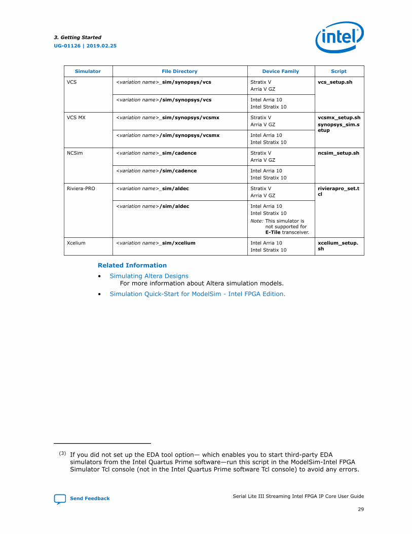
Simulator File Directory Device Family Script
VCS <variation name>_sim/synopsys/vcs Stratix VArria V GZ
vcs_setup.sh
<variation name>/sim/synopsys/vcs Intel Arria 10Intel Stratix 10
VCS MX <variation name>_sim/synopsys/vcsmx Stratix VArria V GZ
vcsmx_setup.shsynopsys_sim.setup
<variation name>/sim/synopsys/vcsmx Intel Arria 10Intel Stratix 10
NCSim <variation name>_sim/cadence Stratix VArria V GZ
ncsim_setup.sh
<variation name>/sim/cadence Intel Arria 10Intel Stratix 10
Riviera-PRO <variation name>_sim/aldec Stratix VArria V GZ
rivierapro_set.tcl
<variation name>/sim/aldec Intel Arria 10Intel Stratix 10Note: This simulator is
not supported forE-Tile transceiver.
Xcelium <variation name>_sim/xcelium Intel Arria 10Intel Stratix 10
xcelium_setup.sh
Related Information
• Simulating Altera DesignsFor more information about Altera simulation models.
• Simulation Quick-Start for ModelSim - Intel FPGA Edition.
(3) If you did not set up the EDA tool option— which enables you to start third-party EDAsimulators from the Intel Quartus Prime software—run this script in the ModelSim-Intel FPGASimulator Tcl console (not in the Intel Quartus Prime software Tcl console) to avoid any errors.
3. Getting Started
UG-01126 | 2019.02.25
Send Feedback Serial Lite III Streaming Intel FPGA IP Core User Guide
29
4. Serial Lite III Streaming IP Core Design ExamplesIntel offers design examples that you can simulate, compile, and test in hardware.
The implementation of the Serial Lite III Streaming IP on hardware requires additionalcomponents specific to the targeted device.
4.1. Serial Lite III Streaming IP Core Design Example for IntelStratix 10 Devices
The Serial Lite III Streaming IP core offers design examples that you can generatethrough the IP catalog in the Intel Quartus Prime Pro Edition software.
For detailed information about the Serial Lite III Streaming IP design examples, referto Serial Lite III Streaming IP Core Design Example User Guide for Intel Stratix 10Devices.
Related Information
Serial Lite III Streaming IP Core Design Example User Guide for Intel Stratix 10Devices
4.2. Serial Lite III Streaming IP Core Design Example for Intel Arria10 Devices
The Serial Lite III Streaming IP core offers design examples that you can generatethrough the IP catalog in the Intel Quartus Prime Pro Edition software.
For detailed information about the Serial Lite III Streaming IP design examples, referto Serial Lite III Streaming IP Core Design Example User Guide for Intel Arria 10Devices.
Related Information
Serial Lite III Streaming IP Core Design Example User Guide for Intel Arria 10 Devices
4.3. Serial Lite III Streaming IP Design Examples for Stratix VDevices
The Serial Lite III Streaming IP core offers design examples that you can generatethrough the IP catalog in the Intel Quartus Prime software.
For detailed information about the Serial Lite III Streaming IP design examples, referto Stratix V Serial Lite III Streaming IP Core Design Example User Guide.
Related Information
Stratix V Serial Lite III Streaming IP Core Design Example User Guide
UG-01126 | 2019.02.25
Send Feedback
Intel Corporation. All rights reserved. Intel, the Intel logo, Altera, Arria, Cyclone, Enpirion, MAX, Nios, Quartusand Stratix words and logos are trademarks of Intel Corporation or its subsidiaries in the U.S. and/or othercountries. Intel warrants performance of its FPGA and semiconductor products to current specifications inaccordance with Intel's standard warranty, but reserves the right to make changes to any products and servicesat any time without notice. Intel assumes no responsibility or liability arising out of the application or use of anyinformation, product, or service described herein except as expressly agreed to in writing by Intel. Intelcustomers are advised to obtain the latest version of device specifications before relying on any publishedinformation and before placing orders for products or services.*Other names and brands may be claimed as the property of others.
ISO9001:2015Registered

5. Serial Lite III Streaming IP Core Functional DescriptionThe Serial Lite III Streaming IP core implements a protocol that defines streamingdata encapsulation at the link layer and data encoding at the physical layer. Thisprotocol integrates transparently with existing hardware and provides a reliable datatransfer mechanism in applications that do not need additional layers between thedata link and application.
5.1. IP Core Architecture
The Serial Lite III Streaming IP core has three variations:
• Source (simplex transmitter)—formats streaming data from the user applicationand transmits the data over serial links.
• Sink (simplex receiver)—receives the serial stream data from serial links, removesany formatting information, and delivers the data to the user application.
• Duplex (transmitter and receiver)—composed of both the source and sink cores.The streaming data can be transmitted and received in both directions.
All three variations include the L-Tile/H-Tile Transceiver Native PHY Intel Stratix 10FPGA IP core in Interlaken mode for Intel Stratix 10 devices, Transceiver Native PHYIntel Arria 10/Intel Cyclone 10 GX FPGA IP core in Interlaken mode in Intel Arria 10devices, or Interlaken PHY v18.1 IP core for Stratix V and Arria V GZ devices thatutilizes hardened PCS and PMA modules. Source only and sink only variants are notavailable if you select E-Tile as the transceiver. The source and sink cores use theTransceiver Native PHY or Interlaken PHY v18.1 IP cores in simplex mode, and theduplex core uses the Transceiver Native PHY or Interlaken PHY v18.1 IP core in duplexmode.
Table 18. IP Core and Functions
Source Core Sink Core
• Data encapsulation• Generation and insertion of Idle Control Words• Lane striping for multi-lane link• User synchronization and burst marker insertion
• Multi-lane alignment• Data decapsulation• Idle Control Words removal• Lane de-striping• User synchronization and burst marker demultiplexing
UG-01126 | 2019.02.25
Send Feedback
Intel Corporation. All rights reserved. Intel, the Intel logo, Altera, Arria, Cyclone, Enpirion, MAX, Nios, Quartusand Stratix words and logos are trademarks of Intel Corporation or its subsidiaries in the U.S. and/or othercountries. Intel warrants performance of its FPGA and semiconductor products to current specifications inaccordance with Intel's standard warranty, but reserves the right to make changes to any products and servicesat any time without notice. Intel assumes no responsibility or liability arising out of the application or use of anyinformation, product, or service described herein except as expressly agreed to in writing by Intel. Intelcustomers are advised to obtain the latest version of device specifications before relying on any publishedinformation and before placing orders for products or services.*Other names and brands may be claimed as the property of others.
ISO9001:2015Registered

Figure 7. Serial Lite III Streaming IP core with Source and Sink Cores
AdaptationModule
PHY IPTransmitCore (1)
Serial Lite III Streaming Source
SourceReconfiguration
ControllerInterface
Source UserInterface
AdaptationModule
PHY IPReceiveCore (1)
Serial Lite III Streaming Sink
SinkReconfigurationControllerInterface
Sink UserInterfaceAlignment
Module
NLanes
Note:1. Native PHY IP core for Intel Arria 10 and Intel Stratix 10 devices and Interlaken PHY IP core for Stratix V and Arria V GZ devices.
ApplicationModule
ApplicationModule
Figure 8. Serial Lite III Streaming IP Core Duplex Core
ApplicationModule
AdaptationModule
PHY IPDuplexCore (1)
Serial Lite III Streaming Duplex
SourceReconfiguration
ControllerInterface
Source UserInterface
AdaptationModule
PHY IPDuplexCore (1)
Serial Lite III Streaming Duplex
SinkReconfigurationControllerInterface
Sink UserInterfaceAlignment
Module
NLanes
NLanes
AdaptationModule Alignment
Module
Sink UserInterface
ApplicationModule
AdaptationModule Source User
Interface
Note:1. Native PHY IP core for Intel Arria 10 and Intel Stratix 10 devices and Interlaken PHY IP core for Stratix V and Arria V GZ devices.
ApplicationModule
ApplicationModule
Related Information
• Intel Arria 10 Transceiver PHY User GuideFor more information about the Intel Arria 10 Native PHY IP core.
• Intel Stratix 10 L- and H-Tile Transceiver PHY User GuideFor more information about the Stratix 10 L- and H-Tile Native PHY IP core.
• Intel Stratix 10 E-Tile Transceiver PHY User GuideFor more information about the Intel Stratix 10 E-Tile Native PHY IP core.
• V-Series Transceiver PHY IP Core User Guide
5.1.1. Serial Lite III Streaming Source Core
The source core consists of four major functional blocks (the implementation variesdepending on the clocking mode):
• Source application module
• Source adaptation module
• L-Tile/H-Tile Transceiver Native PHY Intel Stratix 10 FPGA IP and TransceiverNative PHY IP TX core for Intel Arria 10 - Interlaken mode
• Interlaken PHY v18.1 IP TX core (Stratix V and Arria V GZ devices)
• Clock generator (in the standard clocking mode for Intel Arria 10, Stratix V, andArria V GZ devices)
Related Information
• Standard Clocking Mode in Serial Lite III Streaming Intel FPGA IP Core (IntelStratix 10 Devices) on page 75
5. Serial Lite III Streaming IP Core Functional Description
UG-01126 | 2019.02.25
Serial Lite III Streaming Intel FPGA IP Core User Guide Send Feedback
32

• Standard Clocking Mode in Intel Arria 10, Stratix V, and Arria V Devices on page79
• Advanced Clocking Mode Structure for Serial Lite III Streaming Intel FPGA IP Core(Intel Stratix 10 Devices) on page 82
• Advanced Clocking Mode Structure For Intel Arria 10, Stratix V, and Arria VDevices on page 85
5.1.1.1. Source Application Module
The application module performs the following functions:
• Burst encapsulation—inserts burst control words into the data stream to define thebeginning and the end of streaming data bursts.
• Idle insertion—inserts idle control words into all lanes of the data stream interface.
5.1.1.2. Source Adaptation Module
This module provides adaptation logic between the application module and the L-Tile/H-Tile Transceiver Native PHY Intel Stratix 10 FPGA IP core or Transceiver NativePHY in Intel Arria 10 devices or Interlaken PHY v18.1 IP (Stratix V and Arria V GZdevices) core. The adaptation module performs the following functions:
• Rate adaptation—includes a dual-clock FIFO buffer to cushion the Interlaken PHYv18.1 IP core's burst read requests and to provide a streaming user writeinterface. The FIFO also transfers streaming data between the user_clock andtx_coreclkin clock domains.
• Control signal translation—include state machines that map the control signalsemantics on the framing interface(4) to the semantics of the Transceiver NativePHY or Interlaken PHY v18.1 IP core TX interface.
• Non-user idle insertion—inserts non-user idle control words in the absence of userdata to manage the minimum data rate requirements of the Interlaken protocol.The control words are removed by the sink adaptation module in the Serial Lite IIIStreaming IP core link partner.
• ECC correction and ECC fatal error detection
5.1.1.3. Interlaken PHY IP TX Core or Native PHY IP TX Core - Interlaken Mode
For Intel Arria 10 and Intel Stratix 10 with L-tile and H-tile devices, this block is aninstance of the Native PHY IP core configured for Interlaken - TX only operation. ThePMA width for Interlaken mode is 64 bits.
For Stratix V and Arria V GZ devices, the Interlaken PHY IP TX core is an instance ofthe Interlaken PHY IP core configured for TX only operation. The PMA width forInterlaken mode is 40 bits. The core requires a Transceiver Reconfiguration Controllerfor transceiver calibration. The number of channels programmed for configuration inthe Transceiver Reconfiguration Controller depends on the IP core's operation mode.For example, if the design is a source core only design or a duplex core design, thereconfiguration interfaces is equal to the number of lanes x 2.
(4) The framing interface is to frame every data burst with the Start of Burst, Sync, and End ofBurst, and sequence them to the PHY interface.
5. Serial Lite III Streaming IP Core Functional Description
UG-01126 | 2019.02.25
Send Feedback Serial Lite III Streaming Intel FPGA IP Core User Guide
33

Related Information
• Intel Arria 10 Transceiver PHY User GuideFor more information about the Intel Arria 10 Native PHY IP core.
• Intel Stratix 10 L- and H-Tile Transceiver PHY User GuideFor more information about the Stratix 10 L- and H-Tile Native PHY IP core.
• Intel Stratix 10 E-Tile Transceiver PHY User GuideFor more information about the Intel Stratix 10 E-Tile Native PHY IP core.
• V-Series Transceiver PHY IP Core User GuideFor more information about the Interlaken PHY IP core and reconfigurationcontroller.
5.1.1.4. Source Clock Generator
When you use standard clocking mode for the user interface, the IP core provides aclock generator to generate the user clock (user_clock) and the Intel Arria 10Transceiver Native PHY (tx_coreclockin) or Interlaken PHY v18.1 IP (tx_clkout)core clock signals. This clock generator consists of a fPLL (Stratix V and Arria V GZ) orI/O PLL (Intel Arria 10) and a state machine responsible for clocks generation andreset sequencing. The user_clock_reset is not released until the fPLL or I/O PLL islocked. The module is used in the standard clocking mode only.
Note: For Intel Stratix 10 devices, the tx_clkout signal provides the clock for L-Tile/H-TileTransceiver Native PHY Intel Stratix 10 IP core clock signal (tx_coreclockin)because there is no clock generator module in the Serial Lite III Streaming IP core.
Figure 9. Clock Generator Block Diagram
ResetState
Machine
fPLL/IO PLLphy_mgmt_clk_reset tx_coreclkinuser_clock
lock
user_clock_reset
tx_clkout
• For all Stratix V and Arria V GZ devices, the fPLL generates the user_clock/user_clock_tx and tx_coreclkin based on fixed ratios determined by theSerial Lite III Streaming parameter editor.
• For Intel Arria 10 devices, the I/O PLL generates the user_clock/user_clock_tx based on a fixed ratio, however, the tx_coreclkin operates atthe same frequency as tx_clkout.
Related Information
• Standard Clocking Mode in Serial Lite III Streaming Intel FPGA IP Core (IntelStratix 10 Devices) on page 75
5. Serial Lite III Streaming IP Core Functional Description
UG-01126 | 2019.02.25
Serial Lite III Streaming Intel FPGA IP Core User Guide Send Feedback
34
• Standard Clocking Mode in Intel Arria 10, Stratix V, and Arria V Devices on page79
• Advanced Clocking Mode Structure for Serial Lite III Streaming Intel FPGA IP Core(Intel Stratix 10 Devices) on page 82
• Advanced Clocking Mode Structure For Intel Arria 10, Stratix V, and Arria VDevices on page 85
• Sink Clock Generator on page 36
5.1.2. Serial Lite III Streaming Sink Core
The sink core consists of five major functional blocks:
• L-Tile/H-Tile Transceiver Native PHY Intel Stratix 10 FPGA IP and TransceiverNative PHY IP RX core for Intel Arria 10 - Interlaken mode
• Interlaken PHY v18.1 IP RX core (Stratix V or Arria V GZ devices)
• Lane alignment module
• Sink adaptation module (standard clocking mode only)
• Sink application module
• Clock generator (in the standard clocking mode for Intel Arria 10, Stratix V, andArria V GZ devices)
Related Information
• Standard Clocking Mode in Serial Lite III Streaming Intel FPGA IP Core (IntelStratix 10 Devices) on page 75
• Standard Clocking Mode in Intel Arria 10, Stratix V, and Arria V Devices on page79
• Advanced Clocking Mode Structure for Serial Lite III Streaming Intel FPGA IP Core(Intel Stratix 10 Devices) on page 82
• Advanced Clocking Mode Structure For Intel Arria 10, Stratix V, and Arria VDevices on page 85
5.1.2.1. Sink Application Module
The sink application module performs the following functions:
• Strips the Interlaken protocol bursts encapsulation from the received parallel datastream and sends the data to the sink adaptation module.
• Decodes idle control words inserted by the source application module when thedata stream is not available and indicates the data unavailability at the source bydeasserting the output valid signal at the user interface.
The encapsulation stripping process removes burst control words that define thebeginning and the end of streaming data bursts from the data stream. This processadjusts the received data stream to repack the data words into a contiguoussequence.
• In the standard clocking mode (pure streaming), the decoding process checks thereceived data stream to detect idle control words that the source applicationmodule inserts. When the sink application module detects the idle control words, itdeasserts the valid signal on the user interface until it receives valid userstreaming data.
5. Serial Lite III Streaming IP Core Functional Description
UG-01126 | 2019.02.25
Send Feedback Serial Lite III Streaming Intel FPGA IP Core User Guide
35

• In the advanced clocking mode, the sink application module does not insert ordelete any idle words. Instead, the sink application module deasserts the outputvalid signal to indicate an absence of data coming from the sink adaptationmodule.
5.1.2.2. Sink Adaptation Module
The sink adaptation module provides rate adaptation logic between the applicationmodule and the streaming interface. The adaptation module implements the followingfunctions:
• In standard clocking mode, the FIFO buffers help transfer data between therx_coreclkin and user_clock domains.
• Interlaken framing layer stripping—strips Interlaken framing layer symbols anddiagnostic control words from the data stream.
5.1.2.3. Lane Alignment Module
The lane alignment module interfaces with the Native PHY or Interlaken PHY IP core toaccess incoming data. This module removes lane skew from the incoming serial datastreams and aligns various lanes using the Interlaken's synchronization marker. Afteralignment is achieved, the module continuously monitors the synchronization markersin the Interlaken meta frames for any loss of alignment.
5.1.2.4. Interlaken PHY IP RX Core or Native PHY IP RX Core - Interlaken Mode
For Intel Arria 10 and Intel Stratix 10 L-tile and H-tile devices, this block is an instanceof the Native PHY IP core configured for Interlaken - RX only operation. The PMA widthfor Interlaken mode is 64 bits.
For Stratix V and Arria V GZ devices, the Interlaken module is an instance of theInterlaken PHY IP core configured for RX only operation, and is generated by the IntelQuartus Prime parameter editor. The core requires a Stratix V/Arria V GZ TransceiverReconfiguration Controller for transceiver calibration. The reconfiguration interface sizeis initially equal to the number of transceiver channels that the sink core uses, whichis the number of lanes. The PMA width is 40 bits.
Related Information
• Intel Arria 10 Transceiver PHY User GuideFor more information about the Intel Arria 10 Native PHY IP core.
• Intel Stratix 10 L- and H-Tile Transceiver PHY User GuideFor more information about the Stratix 10 L- and H-Tile Native PHY IP core.
• Intel Stratix 10 E-Tile Transceiver PHY User GuideFor more information about the Intel Stratix 10 E-Tile Native PHY IP core.
• V-Series Transceiver PHY IP Core User GuideFor more information about the Interlaken PHY IP core and reconfigurationcontroller..
5.1.2.5. Sink Clock Generator
The clock generator is similar to the clock generator in the source core, and is onlyinstantiated in standard clocking mode. The clock generator synthesizes the user clock(user_clock) and core clock (rx_coreclkin) signals from the Native PHY IP core
5. Serial Lite III Streaming IP Core Functional Description
UG-01126 | 2019.02.25
Serial Lite III Streaming Intel FPGA IP Core User Guide Send Feedback
36

(Intel Arria 10 devices) or Interlaken PHY IP (Stratix V and Arria V GZ devices) core'soutput clock signal. The clock generator consists of a fPLL or I/O PLL and a statemachine responsible for clock generation and reset sequencing.
Note: For Intel Stratix 10 devices, the rx_clkout signal provides the clock for core clocksignal (rx_coreclockin) because there is no clock generator module in the IP core.
• For all Stratix V and Arria V GZ devices, the fPLL generates the user_clock/user_clock_rx and rx_coreclkin based on fixed ratios determined by the IPcore's parameter editor.
• For Intel Arria 10 devices, the I/OPLL generates the user_clock/user_clock_rx based on a fixed ratio, however, the rx_coreclkin operates atthe same frequency as rx_clkout.
Related Information
• Standard Clocking Mode in Serial Lite III Streaming Intel FPGA IP Core (IntelStratix 10 Devices) on page 75
• Standard Clocking Mode in Intel Arria 10, Stratix V, and Arria V Devices on page79
• Advanced Clocking Mode Structure for Serial Lite III Streaming Intel FPGA IP Core(Intel Stratix 10 Devices) on page 82
• Advanced Clocking Mode Structure For Intel Arria 10, Stratix V, and Arria VDevices on page 85
• Source Clock Generator on page 34
5.1.3. Serial Lite III Streaming IP Core Duplex Core
For Intel Arria 10 and Intel Stratix 10 devices, the duplex core consists of source andsink cores interfaced with the Transceiver Native PHY in Intel Arria 10 devices, L-Tile/H-Tile Transceiver Native PHY Intel Stratix 10, and Intel Stratix 10 E-TileTransceiver Native PHY FPGA IP cores in PCS gearbox mode.
For Stratix V and Arria V GZ devices, the duplex core is composed of source and sinkcores interfaced with the Interlaken PHY v18.1 IP core in duplex mode.
5.1.4. Interlaken PHY IP Duplex Core or Native PHY IP Duplex Core -Interlaken Mode or PCS Gearbox Mode
For Intel Arria 10 and Intel Stratix 10 devices, this block is an instance of the NativePHY IP core configured for duplex Interlaken operation. The PMA width for Interlakenmode is 64 bits.
For Stratix V and Arria V GZ devices, the Interlaken module is an instance of theInterlaken PHY IP core configured for duplex operation, and is generated by the IntelQuartus Prime parameter editor. The core requires a Stratix V/Arria V GZ TransceiverReconfiguration Controller for transceiver calibration. The duplex core initially requiresas many reconfiguration interfaces as the number of lanes that the IP core uses plusone for the TX PLL. The PMA width is 40 bits.
5. Serial Lite III Streaming IP Core Functional Description
UG-01126 | 2019.02.25
Send Feedback Serial Lite III Streaming Intel FPGA IP Core User Guide
37

Related Information
• Intel Arria 10 Transceiver PHY User GuideFor more information about the Intel Arria 10 Native PHY IP core.
• Intel Stratix 10 L- and H-Tile Transceiver PHY User GuideFor more information about the Stratix 10 L- and H-Tile Native PHY IP core.
• Intel Stratix 10 E-Tile Transceiver PHY User GuideFor more information about the Intel Stratix 10 E-Tile Native PHY IP core.
• V-Series Transceiver PHY IP Core User GuideFor more information about the Interlaken PHY IP Core.
5.1.5. Intel Stratix 10, Intel Arria 10, Stratix V, and Arria V GZ Variations
The table summarizes the differences between the Serial Lite III Streaming IP cores inIntel Stratix 10, Intel Arria 10, Stratix V, and Arria V GZ devices.
Table 19. Differences between Intel Stratix 10, Intel Arria 10, Stratix V, and Arria V GZ
Implementation Intel Stratix 10 Intel Arria 10 Stratix V/Arria V GZ
Internal clock generator forStandard Clocking Mode
Not included.User clock is provided byuser.Use HSSI refclk to drive fPLLto generate the user clock.You must share the HSSIrefclk with the L-tile/H-tiletransceiver TX PLL refclk toeliminate PPM differencebetween user clock domainand core clock domain.
Included.The IP core uses IOPLL togenerate the user clock.
Included.The IP core uses FPLL togenerate the user clock.
Control Status Registers(CSR) for MAC
Included. Not included.Only CSR for transceiver isavailable.
Not included.Only CSR for transceiver isavailable.
Interrupts Included. Not included. Not included.
Transceiver transmit PLL Not included Not included. Included.
Transceiver reconfigurationcontroller
Not required. Not required. Required.
PMA width 64 64 40
Hardware DemonstrationDesign Example
Included. Included. Included (for Stratix V only)
When you create an instance of the IP core, it dynamically generates an exampletestbench. This testbench has the same configuration as the IP core instance exceptfor the Burst Gap parameter.
For Intel Arria 10 and Intel Stratix 10 L-tile/H-tile devices, the Native PHY IP core(Interlaken mode) requires an external transmit PLL. Instantiate the external transmitPLLs and then connect the transmit serial clock output to the tx_serial_clk input.The Serial Lite III Streaming IP core uses a transmit serial clock input bus(tx_serial_clk) and tx_pll_locked input to connect the external transmit PLL tothe Intel Arria 10 Native PHY IP core. Refer to the Intel Arria 10 Transceiver PHY UserGuide and Intel Stratix 10 L- and H-Tile Transceiver PHY User Guide for moreinformation.
5. Serial Lite III Streaming IP Core Functional Description
UG-01126 | 2019.02.25
Serial Lite III Streaming Intel FPGA IP Core User Guide Send Feedback
38

Related Information
• Standard Clocking Mode in Serial Lite III Streaming Intel FPGA IP Core (IntelStratix 10 Devices) on page 75
• Standard Clocking Mode in Intel Arria 10, Stratix V, and Arria V Devices on page79
• Advanced Clocking Mode Structure for Serial Lite III Streaming Intel FPGA IP Core(Intel Stratix 10 Devices) on page 82
• Advanced Clocking Mode Structure For Intel Arria 10, Stratix V, and Arria VDevices on page 85
• Signals on page 52
• Intel Arria 10 Transceiver PHY User GuideFor more information about the Intel Arria 10 Native PHY IP core.
• V-Series Transceiver PHY IP Core User GuideFor more information about the Interlaken PHY IP Core.
• AN809: Intel FPGA SerialLite III IP Core Feature and Interface Differencesbetween Intel Stratix 10, Intel Arria 10, and Stratix V
5.2. Transmission Overheads and Lane Rate Calculations
The Serial Lite III Streaming IP core lane data rate (transceiver data rate) iscomposed of the input data rate and transmission overheads.
Lane Rate = Input Data Rate + Transmission Overheads (10% of Input Data Rate)
The parameter editor uses the above equation to ensure that the lane rate is withinthe maximum supported transceiver lane rates. This puts an upper limit on the inputdata rate or the user clock frequency, where the user clock frequency equates to:
User Clock Frequency = Input Data Rate/64
The Serial Lite III Streaming IP core uses the Interlaken protocol for transferring dataand therefore incurs encoding and metaframe overheads.
In the standard clocking mode, the IP core employs an fPLL or I/O PLL for clockgeneration. To ensure that the fPLL or I/O PLL generates the clock as close as possibleto the user clock that you have specified, the fPLL or I/O PLL incurs additionaloverheads. The transmission overheads can thus be derived in the following functions:
Transmission Overheads = Maximum (Interlaken Overheads + fPLL or I/O PLL Overheads) where Interlaken Overheads = [MetaFrame Length /(MetaFrame length - 4)]* 67/64
Therefore, the IP core standard clocking mode lane data rate can be calculated withthe following equation:
Lane Data Rate in Standard Clocking Mode = (User Clock Frequency × 64) × 1.1where 1.1 is referring to additional 10% of Input Data Rate as the transmission overheads.
5. Serial Lite III Streaming IP Core Functional Description
UG-01126 | 2019.02.25
Send Feedback Serial Lite III Streaming Intel FPGA IP Core User Guide
39

In the advanced clocking mode, the transmission overheads equals the Interlakenoverheads because no fPLL or IOPLL is present. Therefore, the lane rate in advancedclocking mode equals:
Lane Rate = Input Data Rate × Interlaken overheads
Tip: You can obtain the Serial Lite III Streaming IP Core Function Data Efficiency Calculatorfor 28 nm Intel FPGA devices from your local Intel sales representative.
Table 20. Example of Transmission Overheads and Lane Rate Calculations per ClockingModesThis example is based on 12.5 Gbps lane rate with metaframe length of 200.
Parameters Standard Clocking Mode Advanced Clocking Mode
Lane rate 12.5 Gbps 12.5 Gbps
Interlaken overheads [Metaframe length/(metaframe length- 4)] * (67/64)200 / (200 - 4) * (67/64) = 1.06824
[Metaframe length/(metaframe length- 4)] * (67/64)200 / (200 - 4) * (67/64) = 1.06824
Transmission overheads 1.1 Interlaken overheads
Input data rate Lane rate/transmission overheads12.5 Gbps/1.1 = 11.364 Gbps
Lane rate/transmission overheads12.5 Gbps/1.06824 = 11.701 Gbps
User clock frequency Input data rate/6411.364 Gbps/64 = 177.5625 MHz
Input data rate/6411.701 Gbps/64 = 182.828 MHz
5.3. Reset
Intel Arria 10, Stratix V and Arria V GZ Reset Scheme
Each core has a separate active high reset signal, core_reset, that asynchronouslyresets all logic in the core.
Each core also includes the Native PHY or Interlaken PHY IP reset signal,phy_mgmt_clk_reset. This reset signal must be on the same clock domain as theclock used to drive the reconfiguration controllers, phy_mgmt_clk. The Native PHY orInterlaken PHY IP core requires the assertion of this reset signal to synchronize withthe reconfiguration controller reset signal.
Note: Intel recommends using the same reset signals for both the Native PHY or InterlakenPHY IP core and the reconfiguration controller.
When the phy_mgmt_clk_reset or core_reset signal is asserted on the sourcecore, the sink deasserts the link_up_rx signal. However, there is no additionalindication on the sink core whether the last transmitted burst has bad data. Thesource core reinitializes the internal reset sequence when the phy_mgmt_clk_resetor core_reset signal is deasserted. Once the internal reset sequence is complete,the core asserts the link_up_tx signal to indicate that the core initialization iscomplete and is ready to transmit user data.
Note: Intel recommends that you wait for an additional 30 µs on the source core beforesending any valid Avalon-ST data cycle. This is to ensure that the sink core hassufficient time to assert the link_up_rx signal.
5. Serial Lite III Streaming IP Core Functional Description
UG-01126 | 2019.02.25
Serial Lite III Streaming Intel FPGA IP Core User Guide Send Feedback
40
Intel Stratix 10 L-tile/H-tile Transceivers Reset Scheme
For Intel Stratix 10 L-tile/H-tile transceivers devices, the IP core uses thephy_mgmt_clk_reset signal to reset all the modules in the IP core anduser_clock_reset signal to reset the user clock domain modules e.g. transmit andreceive FIFO.
You may also trigger a reset to the IP core by writing into the reset controller registerin the PHY:
• Writing 1 to CSR address 0x02E2 bit 3 to initiate a TX digital reset and bit 1 toinitiate a RX digital reset
• Writing 1 to CSR address 0x02E2 bit 2 to initiate a TX analog reset and bit 0 toinitiate a RX analog reset
Intel Stratix 10 E-tile Transceivers Reset Scheme
E-Tile transceivers have separate reset procedures for analog reset and digital reset.
You can use the PMA attribute code 0x0001 on the AVMM reconfiguration bus toenable or disable the PMA. Disabling the PMA puts it in reset. Digital reset can beasserted using the digital reset controller in the Native PHY IP.
Use the following guidelines to provide a proper reset to the IP core. These guidelinesare applicable to Intel Stratix 10 L-tile/H-tile/E-tile transceivers devices:
• Use the same reset signals for both the source and sink user clock domainmodules.
• Synchronize the user_clock_reset signals with phy_mgmt_clock_resetsignal assertion.
• Use the phy_mgmt_clk_reset signal to reset the configuration and statusregisters.
• Ensure all clocks are toggling in a correct rate before de-asserting any resetsignals.
Related Information
Intel Stratix 10 E-Tile Transceiver PHY User GuideMore information about resetting the Intel Stratix 10 E-Tile transceiver.
5.4. Link-Up Sequence
Link-up Sequence for Intel Stratix 10 L-tile/H-tile Transceivers, Intel Arria10, Stratix V, and Arria V Devices
For source core:
5. Serial Lite III Streaming IP Core Functional Description
UG-01126 | 2019.02.25
Send Feedback Serial Lite III Streaming Intel FPGA IP Core User Guide
41
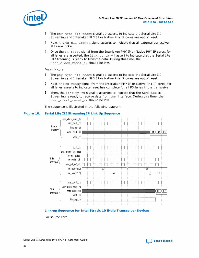
1. The phy_mgmt_clk_reset signal de-asserts to indicate the Serial Lite IIIStreaming and Interlaken PHY IP or Native PHY IP cores are out of reset.
2. Next, the tx_pll_locked signal asserts to indicate that all external transceiverPLLs are locked.
3. Once the tx_ready signal from the Interlaken PHY IP or Native PHY IP cores, forall lanes are asserted, the link_up_tx will assert to indicate that the Serial LiteIII Streaming is ready to transmit data. During this time, theuser_clock_reset_tx should be low.
For sink core:
1. The phy_mgmt_clk_reset signal de-asserts to indicate the Serial Lite IIIStreaming and Interlaken PHY IP or Native PHY IP cores are out of reset.
2. Next, the rx_ready signal from the Interlaken PHY IP or Native PHY IP cores, forall lanes asserts to indicate reset has complete for all RX lanes in the transceiver.
3. Then, the link_up_rx signal is asserted to indicate that the Serial Lite IIIStreaming is ready to receive data from user interface. During this time, theuser_clock_reset_rx should be low.
The sequence is illustrated in the following diagram.
Figure 10. Serial Lite III Streaming IP Link Up Sequence
3F
i_clk_tx
phy_mgmt_clk_reset
tx_serial_clk
xcvr_pll_ref_clktx_ready[5:0]
rx_ready[5:0]
tx_pll_locked
D3
user_clock_reset_txuser_clock_tx
data_tx[383:0]
valid_tx
link_up_txSource interface
PHY interface
user_clock_rx
user_clock_reset_rx
valid_rx
link_up_rx
data_rx[383:0]Sink interface
3F
00
00
D1 D2
D1 D2
Link-up Sequence for Intel Stratix 10 E-tile Transceiver Devices
For source core:
5. Serial Lite III Streaming IP Core Functional Description
UG-01126 | 2019.02.25
Serial Lite III Streaming Intel FPGA IP Core User Guide Send Feedback
42
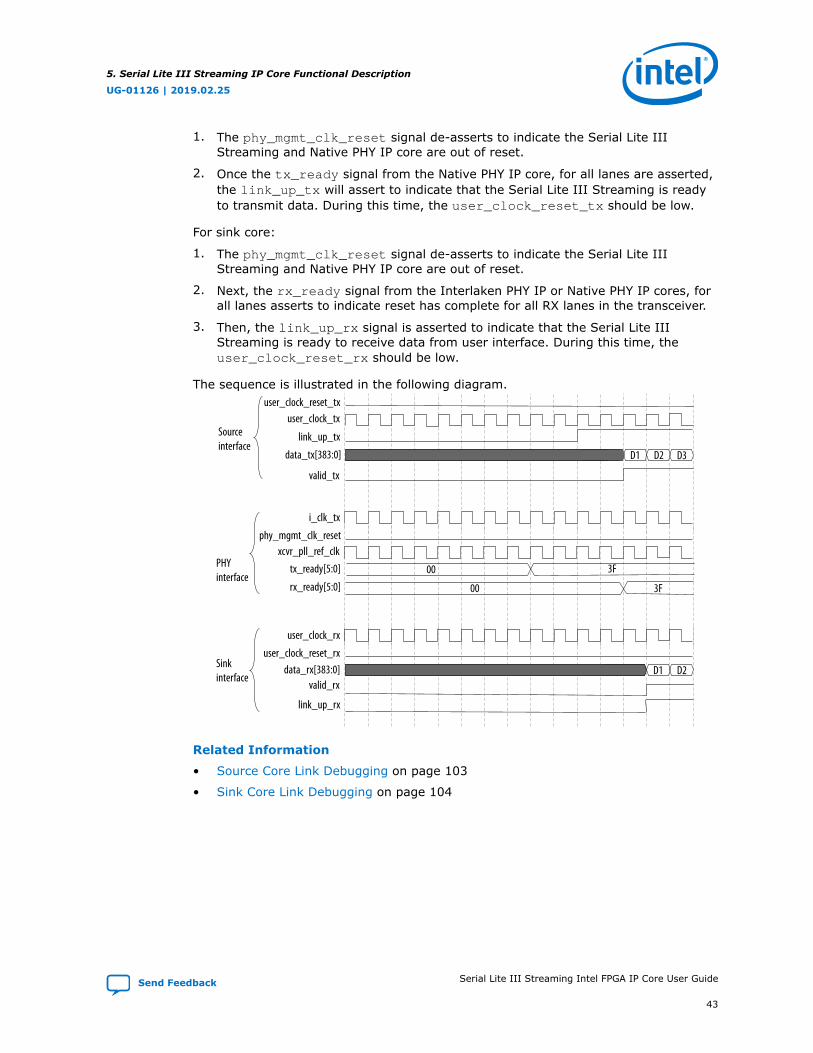
1. The phy_mgmt_clk_reset signal de-asserts to indicate the Serial Lite IIIStreaming and Native PHY IP core are out of reset.
2. Once the tx_ready signal from the Native PHY IP core, for all lanes are asserted,the link_up_tx will assert to indicate that the Serial Lite III Streaming is readyto transmit data. During this time, the user_clock_reset_tx should be low.
For sink core:
1. The phy_mgmt_clk_reset signal de-asserts to indicate the Serial Lite IIIStreaming and Native PHY IP core are out of reset.
2. Next, the rx_ready signal from the Interlaken PHY IP or Native PHY IP cores, forall lanes asserts to indicate reset has complete for all RX lanes in the transceiver.
3. Then, the link_up_rx signal is asserted to indicate that the Serial Lite IIIStreaming is ready to receive data from user interface. During this time, theuser_clock_reset_rx should be low.
The sequence is illustrated in the following diagram.
3F
i_clk_tx
phy_mgmt_clk_resetxcvr_pll_ref_clk
tx_ready[5:0]
rx_ready[5:0]
D3
user_clock_reset_txuser_clock_tx
data_tx[383:0]
valid_tx
link_up_txSource interface
PHY interface
user_clock_rx
user_clock_reset_rx
valid_rx
link_up_rx
data_rx[383:0]Sink interface
3F
00
00
D1 D2
D1 D2
Related Information
• Source Core Link Debugging on page 103
• Sink Core Link Debugging on page 104
5. Serial Lite III Streaming IP Core Functional Description
UG-01126 | 2019.02.25
Send Feedback Serial Lite III Streaming Intel FPGA IP Core User Guide
43
5.5. Error Detection, Reporting, and Recovering Mechanism
Table 21. Error Conditions, Core Behavior, Reporting, and Recovering MechanismThis table lists the error conditions that the core detect, their behavior in response to each condition, andavailable reporting mechanisms.
Condition IP Behavior Reporting Mechanism RecoveringMechanism
SourceCore
Burst gaperror
The source detects the burst gapbetween two consecutive bursts does notmatch Required idle cycles betweenbursts parameter setting.The source core asserts the error flag forone clock cycle.
• tx_burst_gap_err of TX Error Statusregister set to 1(only for IntelStratix 10 devices).
• error/error_tx[3] signalasserted.
• err_interrupt/err_interrupt_tx signal asserted(only availablewhentx_burst_gap_err_en of TX ErrorInterrupt Enableregister is set to 1(only for IntelStratix 10 devices).
Make sure the burstgap of the incomingpacket is matching theRequired idle cyclesbetweenburstsparameter.
RateadaptationFIFO bufferoverflow insourceinterface.
There is an overflow on the rateadaptation FIFO buffer in the sourceinterface. The core behavior depends onthe operation mode:• Continuous mode—error is flagged
once an overflow is detected.• Burst mode—error is flagged only
when an overflow occurs during burstdata transfer across the userinterface.
The source core asserts the error flag aslong as the FIFO is in overflow condition.
• adapt_fifo_overflow of TX ErrorStatus register setto 1 (only for IntelStratix 10 devices).
• error/error_tx[0] signalasserted.
• err_interrupt/err_interrupt_tx signal asserted(only availablewhenadapt_fifo_overflow_en of TXError InterruptEnable register isset to 1 (only forIntel Stratix 10devices).
• Assertphy_mgmt_clk_reset to reset the IP.
• Send empty cycle toprevent FIFOoverflow.
continued...
5. Serial Lite III Streaming IP Core Functional Description
UG-01126 | 2019.02.25
Serial Lite III Streaming Intel FPGA IP Core User Guide Send Feedback
44

Condition IP Behavior Reporting Mechanism RecoveringMechanism
ECC fatalerror.
The source core asserts the error flag forone clock cycle when a double bit erroris detected.
• adapt_fifo_overflow of TX ErrorStatus register setto 1 (only for IntelStratix 10 devices).
• error/error_tx[0] signalasserted.
• err_interrupt/err_interrupt_tx signal asserted(only availablewhenecc_err_fatal_en of TX ErrorInterrupt Enableregister is set to 1(only for IntelStratix 10 devices).
Assertphy_mgmt_clk_reset signal to reset the IP.
ECC correctederror.
The source core asserts the error flag forone clock cycle when a single bit error isdetected and corrected.
• ecc_err_corrected of TX ErrorStatus register setto 1 (only for IntelStratix 10 devices).
• error/error_tx[1] signalasserted.
• err_interrupt/err_interrupt_tx signal asserted(only availablewhenecc_err_corrected_en of TX ErrorInterrupt Enableregister is set to 1(only for IntelStratix 10 devices).
—
Source lost oflanealignmenterror
The source core detects a loss of lanealignment during normal operation.
• tx_sync_done_lost of TX ErrorStatus register setto 1 (only for IntelStratix 10 devices).
• err_interrupt/err_interrupt_tx signal asserted(only availablewhentx_sync_donelost_en of TX ErrorInterrupt Enableregister is set to 1(only for IntelStratix 10 devices).
The source coreautomatically re-initialize the link whenthis error occurs.Optionally, you canassertphy_mgmt_clk_reset to reset the IP.
continued...
5. Serial Lite III Streaming IP Core Functional Description
UG-01126 | 2019.02.25
Send Feedback Serial Lite III Streaming Intel FPGA IP Core User Guide
45

Condition IP Behavior Reporting Mechanism RecoveringMechanism
Sink Core RX data error When the sink interface receives databut ready_rx signal is de-asserted.
• rx_data_err ofRX Error Statusregister set to 1(only for IntelStratix 10 devices).
• err_interrupt/err_interrupt_rx signal asserted(only availablewhenrx_data_err_int_en of RX ErrorInterrupt Enableregister is set to 1(only for IntelStratix 10 devices).
—
Lane deskewfatal error
The sink core detects an error when thelane skews across all lanes exceeded thehardware de-skew capability.
• rx_deskew_fatalof RX Error Statusregister set to 1(only for IntelStratix 10 devices).
• err_interrupt/err_interrupt_rx signal asserted(only availablewhenrx_deskew_fatal_int_en of RXError InterruptEnable register isset to 1 (only forIntel Stratix 10devices).
Assertphy_mgmt_clk_reset to reset the IP.Ensure the boardrouting does notexceed 107 UI.
ECC fatalerror.
The sink core asserts the error flag forone clock cycle when a double bit erroris detected.
• ecc_err_fatal ofRX Error Statusregister set to 1(only for IntelStratix 10 devices).
• error/error_rx[N+4]signal asserted.
• err_interrupt/err_interrupt_rx signal asserted(only availablewhenecc_err_fatal_int_en of RX ErrorInterrupt Enableregister is set to 1(only for IntelStratix 10 devices).
Assertphy_mgmt_clk_reset signal to reset the IP.
continued...
5. Serial Lite III Streaming IP Core Functional Description
UG-01126 | 2019.02.25
Serial Lite III Streaming Intel FPGA IP Core User Guide Send Feedback
46
Condition IP Behavior Reporting Mechanism RecoveringMechanism
ECC correctederror.
The sink core asserts the error flag forone clock cycle when a single bit error isdetected and corrected.
• ecc_err_corrected of RX ErrorStatus register setto 1 (only for IntelStratix 10 devices).
• error/error_rx[N+3]signal asserted.
• err_interrupt/err_interrupt_rx signal asserted(only availablewhenecc_err_corrected_int_en of RXError InterruptEnable register isset to 1 (only forIntel Stratix 10devices).
—
RateadaptationFIFO bufferoverflow
There is an overflow on the rateadaptation FIFO buffer in the sinkinterface. The core behavior depends onthe operation mode:• Continuous mode—error is flagged
once an overflow is detected.• Burst mode—error is flagged only
when an overflow occurs during burstdata transfer across the userinterface.
The sink core asserts the error flag aslong as the FIFO is in overflow condition.
• adapt_fifo_overflow of RX ErrorStatus register setto 1 (only for IntelStratix 10 devices).
• error/error_rx[N+2]signal asserted.
• err_interrupt/err_interrupt_rx signal asserted(only availablewhenadapt_fifo_over_flow_int_en ofRX Error InterruptEnable register isset to 1 (only forIntel Stratix 10devices).
—
continued...
5. Serial Lite III Streaming IP Core Functional Description
UG-01126 | 2019.02.25
Send Feedback Serial Lite III Streaming Intel FPGA IP Core User Guide
47

Condition IP Behavior Reporting Mechanism RecoveringMechanism
Lanealignmentfailure duringnormaloperation
The sink core detects a loss of lanealignment during normal operation.The sink core asserts error[N](5) flag forone clock cycle.
• rx_alignment_lostlock of RX ErrorStatus register setto 1 (only for IntelStratix 10 devices).
• error/error_rx[N]signal asserted.
• err_interrupt/err_interrupt_rx signal asserted(only availablewhenrx_alignment_lostlock_int_en ofRX Error InterruptEnable register isset to 1 (only forIntel Stratix 10devices).
The sink coreautomatically re-initialize and re-alignthe link.Optionally, you canassertphy_mgmt_clk_reset to reset the IP.
RX PCS Error One or more errors have occured in agiven meta-frame, as determined byNative PHY PCS logic (in Interlakenmode).These errors could be triggered muchlater (with respect to the user packetsreceived earlier) at the receiving link.Note: If data integrity is critical,
additional error checksum maybe included in the user logic aspart of data payload so that thedownstream user logic candetermine the data integrity atpacket level.
• rx_pcs_err of RXError Statusregister set to 1(only for IntelStratix 10 devices).
• error/error_rx[N-1:0]signal asserted.
• err_interrupt/err_interrupt_rx signal asserted(only availablewhenrx_pcs_err_int_en of RX ErrorInterrupt Enableregister is set to 1(only for IntelStratix 10 devices).
—
Diagnosticcode wordCRC-32 error
The sink core detects a metaframeCRC-32 error on one of the lanes. Theseerrors are reported on a per-lane basisfor diagnostic purposes.The sink core asserts error[N-1:0](5) flagfor one clock cycle.
• rx_crc32err ofRX Error Statusregister set to 1(only for IntelStratix 10 devices).
• error/error_rx[N-1:0]signal asserted.
• err_interrupt/err_interrupt_rx signal asserted(only availablewhenrx_crc32err_int_en of RX ErrorInterrupt Enableregister is set to 1(only for IntelStratix 10 devices).
—
(5) N is the number of lanes.
5. Serial Lite III Streaming IP Core Functional Description
UG-01126 | 2019.02.25
Serial Lite III Streaming Intel FPGA IP Core User Guide Send Feedback
48

5.6. CRC-32 Error Injection
In the Intel Quartus Prime software version 13.1 and later, the Serial Lite IIIStreaming IP core supports CRC error injection with the 10G PCS CRC-32 generator.This feature enables corruption of the CRC-32 value of the CRC-32 generator.
To insert CRC errors for a given lane, the IP interface includes a CRC error injectioncontrol signal. Asserting this control signal inserts CRC errors for all the lanes andtransceivers that have enabled support for error injection. You can enable the CRCerror injection for a specific transceiver channel (Serial Lite III Streaming lane) byprogramming the appropriate transceiver PCS CRAM bit. The provided example designdemonstrates how set the respective CRAM bits using the Nios II processor.
For proper functionality of this feature, you must verify that you are adhering to thefollowing steps:
1. Verify both link_up_tx and link_up_rx are asserted.
2. Verify the user can send/receive normal traffic.
3. After link up, program the transceiver register and verify the register bit (PCSCRAM bit) by reading.
4. With link up, toggle crc_error_inject port to high on the transmitter.
5. Monitor the error_rx output on the receiver.
Related Information
• Intel FPGA Serial Lite III Streaming IP Core Design Example User Guide for IntelStratix 10 Devices
• Intel Arria 10 Serial Lite III Streaming IP Core Design Example User Guide
5.7. FIFO ECC Protection
In the Quartus II software version 13.1 and later, the Serial Lite III Streaming IP corecan be protected from Single-Event Upset (SEU) changes using error correcting code(ECC) protection. You can enable this feature using the ECC protection option in theparameter editor. The ECC protection provides additional error status bits that tell youif the ECC was able to perform a correction from the SEU change or if anuncorrectable error has occurred.
Note: Enabling ECC protection incurs additional logic and latency overhead.
5.8. User Data Interface Waveforms
The following waveforms apply to the Serial Lite III Streaming IP core source userinterface in source-only and duplex cores.
Figure 11. Source Waveform for Burst Mode1800_0020_0000_0* 1800_002* 180* 180** **data[127:0]
start_of_burstend_of_burst
valid
5. Serial Lite III Streaming IP Core Functional Description
UG-01126 | 2019.02.25
Send Feedback Serial Lite III Streaming Intel FPGA IP Core User Guide
49
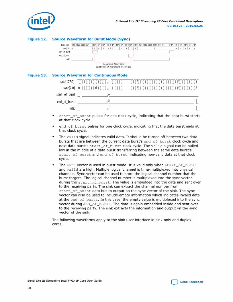
Figure 12. Source Waveform for Burst Mode (Sync)1800_0020_0000_06*data[127:0]
sync[7:0]start_of_burst
end_of_burst
valid
18* 18* 18* 18* 18* 18* 18* 18* 18* 1800_0021_0000_06e1_2000_0021_0* 18* 18* 18* 18* 18* 18*
0 4 0 0 09 3 c a 3 8 a a 8f e
The source sync data are picked up at the start_of_burst and end_of_burst cycle.
5
Figure 13. Source Waveform for Continuous Mode
0 8
* *
**d
data[127:0]
sync[7:0]
start_of_burst
end_of_burst
valid
• start_of_burst pulses for one clock cycle, indicating that the data burst startsat that clock cycle.
• end_of_burst pulses for one clock cycle, indicating that the data burst ends atthat clock cycle.
• The valid signal indicates valid data. It should be turned off between two databursts that are between the current data burst's end_of_burst clock cycle andnext data burst's start_of_burst clock cycle. The valid signal can be pulledlow in the middle of a data burst transferring between the same data burst'sstart_of_burst and end_of_burst, indicating non-valid data at that clockcycle.
• The sync vector is used in burst mode. It is valid only when start_of_burstand valid are high. Multiple logical channel is time-multiplexed into physicalchannels. Sync vector can be used to store the logical channel number that theburst targets. The logical channel number is multiplexed into the sync vectorduring the start_of_burst. The value is embedded into the data and sent overto the receiving party. The sink can extract the channel number fromstart_of_burst data bus to output on the sync vector of the sink. The syncvector can also be used to include empty information which indicates invalid dataat the end_of_burst. In this case, the empty value is multiplexed into the syncvector during end_of_burst. The data is again embedded inside and sent overto the receiving party. The sink extracts the information and output on the syncvector of the sink.
The following waveforms apply to the sink user interface in sink-only and duplexcores.
5. Serial Lite III Streaming IP Core Functional Description
UG-01126 | 2019.02.25
Serial Lite III Streaming Intel FPGA IP Core User Guide Send Feedback
50
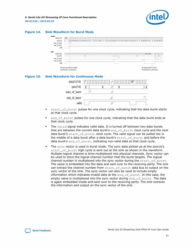
Figure 14. Sink Waveform for Burst Mode
data[127:0]sync[7:0]
start_of_burstend_of_burst
valid
data[127:0]
sync[7:0]start_of_burstend_of_burst
valid
1800* * * * * * * * * * * * * * * * * * * * * * * * * * * * * ** * * * * * * * * * * * * * * * * * * * * * * * * * * * *
0 d 7 0 9 b e 3 2 0 6 9 1 2 7 9 2 c 0 8 5 1 5 3 e 3 d 72 f 1 6 5 4 b 1 9 a 8 e f 4 9 b 8 9 f a 0 d 2 8 4 d *
* * * * * * * * * * * * * * * * * * * * * * * * * * * * * ** * * * * * * * * * * * * * * * * * * 1800_0003_* * * * * * *5 e 3 d
The sink sync data “d” is sent out at the start_of_burst cycle.
The source sync data “d” is picked up at the start_of_burst cycle.
Source
Sink
Figure 15. Sink Waveform for Continuous Mode
data[127:0]
sync[7:0]
start_of_burst
end_of_burst
valid
0 8
* 18*
d8
• start_of_burst pulses for one clock cycle, indicating that the data burst startsat that clock cycle.
• end_of_burst pulses for one clock cycle, indicating that the data burst ends atthat clock cycle.
• The valid signal indicates valid data. It is turned off between two data burststhat are between the current data burst's end_of_burst clock cycle and the nextdata burst's start_of_burst clock cycle. The valid signal can be pulled low inthe middle of a data burst after a data burst's start_of_burst and before thedata burst's end_of_burst, indicating non-valid data at that clock cycle.
• The sync vector is used in burst mode. The sync data picked up at the source'sstart_of_burst high cycle is sent out at the sink as shown in the waveform.Multiple logical channel is time-multiplexed into physical channels. Sync vector canbe used to store the logical channel number that the burst targets. The logicalchannel number is multiplexed into the sync vector during the start_of_burst.The value is embedded into the data and sent over to the receiving party. The sinkcan extract the channel number from start_of_burst data bus to output on thesync vector of the sink. The sync vector can also be used to include emptyinformation which indicates invalid data at the end_of_burst. In this case, theempty value is multiplexed into the sync vector during end_of_burst. The datais again embedded inside and sent over to the receiving party. The sink extractsthe information and output on the sync vector of the sink.
5. Serial Lite III Streaming IP Core Functional Description
UG-01126 | 2019.02.25
Send Feedback Serial Lite III Streaming Intel FPGA IP Core User Guide
51
5.9. Signals
The following tables list all the input and output signals of the Serial Lite III StreamingIP core.
5.9.1. Signals for Intel Stratix 10 Devices
Table 22. Serial Lite III Streaming Source Core Signals for Intel Stratix 10 L-tile and H-tile Devices
Signal Width ClockDomain
Direction Description
tx_serial_clk N N/A Input This signal is a high-speed serial clock input from theexternal transceiver PLL. The width is the same as thenumber of lanes specified in the parameter editor.Each bit of the vector corresponds to serial clock ofthe transmit channel.N represents the number of lanes.
tx_pll_locked 1 N/A Input This signal indicates that all external transceiver PLLsare locked. If more than one external transceiver PLLis required for higher lanes, each instantiation outputsa bit that indicates whether the PLL providing thehigh-speed clock for a corresponding transceiver hasachieved its lock status. The pll_locked outputsignal from the external transceiver PLLs should beANDed together before being input to the IP core.
xcvr_pll_ref_clk 1 N/A Input This signal is the reference clock for the transceivers.
user_clock 1 N/A Input/Output
Clock for data transfers across the source coreinterface.This is an input signal for standard and advancedclocking mode.
user_clock_reset 1 user_clock Input/Output
Asserts this signal to reset all the user clock domainmodule.Available only in Standard Clocking Mode.
link_up 1 user_clock Output The core asserts this signal to indicate that the coreinitialization is complete and is ready to transmit userdata.
data 64xN user_clock Input This vector carries the transmitted streaming data tothe core.N represents the number of lanes.
sync 8 user_clock Input The sync vector is an 8 bit bus. The data value at thestart of a burst and the end of a burst are capturedand transported across the link.The value at the end of a burst is to indicate thenumber of invalid 64-bit word in the previous datacycle. As such, for single-lane configuration, the valueat the end of a burst is expected to be 0.Note: This vector is not associated with Interlaken
channelization or flow control schemes.
valid 1 user_clock Input This single bit signal indicates that the transmittedstreaming data is valid.
ready 1 user_clock Output On interfaces supporting backpressure, the sourceasserts ready to mark the cycles where transfers maytake place. When this signal is asserted on cycle N,cycle (N + readLatency, where readLatency=0) isconsidered a ready cycle.
continued...
5. Serial Lite III Streaming IP Core Functional Description
UG-01126 | 2019.02.25
Serial Lite III Streaming Intel FPGA IP Core User Guide Send Feedback
52
Signal Width ClockDomain
Direction Description
This signal is only asserted after tx_link_up isasserted.Leave unconnected if unused.
start_of_burst 1 user_clock Input When the core is in burst mode operation, assertingthis signal indicates that the information on the datavector is the beginning of a burst.Because continuous mode is one long burst, in thismode the signal is asserted only once at the start ofthe data.
end_of_burst 1 user_clock Input When the core is in burst mode operation, assertingthis signal indicates that the information on the datavector is the end of a burst.You can optionally send an end of burst signal at theend of continuous mode.
error 4 user_clock Output This vector indicates an error or overflow in the sourceadaptation module’s FIFO buffer.• Bit 0: Source adaptation module’s FIFO buffer
overflow• Bit 1: An SEU error occurred and was corrected
(ECC enabled)Don't care (ECC disabled)
• Bit 2: An SEU error occurred and cannot becorrected (ECC enabled)Don't care (ECC disabled)
• Bit 3: A burst gap error occurred due to amismatch in the BURST GAP parameter value andthe gap between end of burst and start of burst.
crc_error_inject 1 user_clock Input This signal forces CRC-32 errors when CRC-32 errorinjection is enabled in the transceiver channels. TheCRC-32 error injection is enabled via the transceiverreconfiguration controller.
err_interrupt 1 phy_mgmt_clk
Output This signal indicates if a transmit error occurs in thecurrent transmission. The signal goes to '1' when anyerror status bit and its associated interrupt enabled bithave been set to '1'. It goes to '0' after all error statusbits with interrupt enabled have been cleared.Leave unconnected if unused.
Table 23. Serial Lite III Streaming Sink Core Signals for Intel Stratix 10 L-tile and H-tile Devices
Signal Width Clock Domain Direction Description
xcvr_pll_ref_clk 1 N/A Input Reference clock for the transceivers.
user_clock 1 N/A Output Clock for data transfers across the sink coreinterface in the standard clocking mode.
user_clock_reset 1 user_clock Output Asserts this signal to reset all the user clockdomain module.Available only in Standard Clocking Mode.
interface_clock 1 core_clock Output Clock for data transfer across the sink coreinterface in the advanced clocking mode.
interface_clock_reset
1 core_clock Output The core asserts this signal when thephy_mgmt_clk_reset signal is high anddeasserts this signal when the reset sequenceis complete in the advanced clocking mode.
continued...
5. Serial Lite III Streaming IP Core Functional Description
UG-01126 | 2019.02.25
Send Feedback Serial Lite III Streaming Intel FPGA IP Core User Guide
53

Signal Width Clock Domain Direction Description
Available only in Advanced Clocking Mode.
link_up 1 Standardclocking:user_clockAdvancedclocking:core_clock
Output The core asserts this signal to indicate that thecore initialization is complete and is ready totransmit user data.When this signal is deasserted, all values inthe data_rx signal is invalid regardless of thevalid_rx signal value. This means even whenthe valid_rx signal is asserted, the data_rxsignal should be treated as invalid whenlink_up_rx is deasserted.
data 64xN Standardclocking:user_clockAdvancedclocking:core_clock
Output This vector carries the transmitted streamingdata from the core.N represents the number of lanes.
sync 8 Standardclocking:user_clockAdvancedclocking:core_clock
Output The sync vector is an 8 bit bus that reflects theSYNC value received from the remote partner.The value at the end of a burst is to indicatethe number of invalid 64-bit word in theprevious data cycle. As such, for single-laneconfiguration, the value at the end of a burst isexpected to be 0.Note: This vector is not associated with
Interlaken channelization or flowcontrol schemes.
valid 1 Standardclocking:user_clockAdvancedclocking:core_clock
Output This single bit signal indicates that the data isvalid.
start_of_burst 1 Standardclocking:user_clockAdvancedclocking:core_clock
Output When the core is in burst mode operation,assertion of this signal indicates that theinformation on the data vector is the beginningof a burst.Because continuous mode is one long burst, inthis mode, the core asserts this signal onlyonce at the start of the data.
end_of_burst 1 Standardclocking:user_clockAdvancedclocking:core_clock
Output When the core is in burst mode operation,assertion of this signal indicates that theinformation on the data vector is the end of aburst.
continued...
5. Serial Lite III Streaming IP Core Functional Description
UG-01126 | 2019.02.25
Serial Lite III Streaming Intel FPGA IP Core User Guide Send Feedback
54
Signal Width Clock Domain Direction Description
error N+5 Standardclocking:user_clockAdvancedclocking:core_clock
Output This vector indicates the state of the sinkadaptation module’s FIFO buffer. N representsthe number of lanes:• [N+4]: An SEU error occurred and cannot
be corrected (ECC enabled); Don't care(ECC disabled)Don't care (for advanced clocking mode)
• [N+3]: An SEU error occurred and wascorrected (ECC enabled); Don't care (ECCdisabled)Don't care (for advanced clocking mode)
• [N+2]: Sink adaptation FIFO overflowDon't care (for advanced clocking mode)
• [N+1]: Don't care. Tied to zero.• [N]: Loss of alignment• [N-1:0]: PCS sync header, multiframe, or
CRC-32 error
ready 1 Standardclocking:user_clockAdvancedclocking:core_clock
Input On interfaces supporting backpressure, thesink asserts ready to mark the cycles wheretransfers may take place. When this signal isasserted on cycle N, cycle (N + readLatency,where readLatency=0) is considered a readycycle.If this signal de-asserts in the middle of a datatransfer, it is considered an erroneouscondition.Leave unconnected if unused.
err_interrupt 1 phy_mgmt_clk Output This signal indicates if a receive error as occurin the current transmission. The signal goes to'1' when any error status bit and its associatedinterrupt enabled bit have been set to '1'. Itgoes to '0' after all error status bits withinterrupt enabled have been cleared.Leave unconnected if unused.
Table 24. Serial Lite III Streaming Duplex Core Signals for Intel Stratix 10 L-tile, H-tile,and E-tile Devices
Signal Width ClockDomain
Direction Description
tx_serial_clk N N/A Input This high-speed serial clock input from the externaltransceiver PLL. The width is the same as thenumber of lanes specified in the parameter editor.Each bit of the vector corresponds to serial clock ofthe transmit channel.N represents the number of lanes.Note: This signal is not available when you select E-
Tile as the transceiver tile.
tx_pll_locked 1 N/A Input This signal indicates that all external transceiver PLLsare locked. If more than one external transceiver PLLis required for higher lanes, each instantiationoutputs a bit that indicates whether the PLL providingthe high-speed clock for a corresponding transceiverhas achieved its lock status. The pll_locked outputsignal from the external transceiver PLLs should beANDed together before being input to the IP core.Note: This signal is not available when you select E-
Tile as the transceiver tile.
continued...
5. Serial Lite III Streaming IP Core Functional Description
UG-01126 | 2019.02.25
Send Feedback Serial Lite III Streaming Intel FPGA IP Core User Guide
55

Signal Width ClockDomain
Direction Description
xcvr_pll_ref_clk 1 N/A Input Reference clock for the transceivers.
user_clock_tx 1 N/A Input Clock for data transfers across the transmit interface.
user_clock_reset_tx
1 user_clock_tx
Input In the standard clocking mode, the core asserts thissignal when the phy_mgmt_clk_reset signal ishigh and deasserts this signal when the resetsequence is complete.In the advanced clocking mode, asserts this signal toreset all user clock domain modules.
link_up_tx 1 Standardclocking:user_clockAdvancedclocking:core_clock
Output The core asserts this signal to indicate that the coreinitialization is complete and is ready to transmituser data.
data_tx 64xN Standardclocking:user_clockAdvancedclocking:core_clock
Input This vector carries the transmitted streaming data tothe core.N represents the number of lanes.
sync_tx 8 Standardclocking:user_clockAdvancedclocking:core_clock
Input The sync vector is an 8 bit bus. The data value at thestart of a burst and at the end of a burst arecaptured and transported across the link.The value at the end of a burst is to indicate thenumber of invalid 64-bit word in the previous datacycle. As such, for single-lane configuration, thevalue at the end of a burst is expected to be 0.Note: This vector is not associated with Interlaken
channelization or flow control schemes.
valid_tx 1 Standardclocking:user_clockAdvancedclocking:core_clock
Input This vector indicates that the data is valid.
start_of_burst_tx 1 Standardclocking:user_clockAdvancedclocking:core_clock
Input When the core is in burst mode operation, assertionof this signal indicates that the information on thedata vector is the beginning of a burst.Because continuous mode is one long burst, in thismode the signal is asserted only once at the start ofthe data.
end_of_burst_tx 1 Standardclocking:user_clockAdvancedclocking:core_clock
Input When the core is in burst mode operation, assertionof this signal indicates that the information on thedata vector is the end of a burst.
error_tx 4 Standardclocking:user_clockAdvancedclocking:core_clock
Output This vector indicates an overflow in the sourceadaptation module’s FIFO buffer.• Bit 0: Source adaptation module’s FIFO buffer
overflow
continued...
5. Serial Lite III Streaming IP Core Functional Description
UG-01126 | 2019.02.25
Serial Lite III Streaming Intel FPGA IP Core User Guide Send Feedback
56

Signal Width ClockDomain
Direction Description
• Bit 1: An SEU error occurred and was corrected(ECC enabled).Don't care (ECC disabled)
• Bit 2: An SEU error occurred and cannot becorrected (ECC enabled).Don't care (ECC disabled)
• Bit 3: A burst gap error occurred due to amismatch in the BURST GAP parameter value andthe gap between end of burst and start of burst.
err_interrupt_tx 1 phy_mgmt_clk
Output This signal indicates if a transmit error occurs in thecurrent transmission. The signal goes to '1' when anyerror status bit and its associated interrupt enabledbit have been set to '1'. It goes to '0' after all errorstatus bits with interrupt enabled have been cleared.Leave unconnected if unused.
ready_tx 1 user_clock Output On interfaces supporting backpressure, the sourceasserts ready to mark the cycles where transfersmay take place. When this signal is asserted on cycleN, cycle (N + readLatency, where readLatency=0) isconsidered a ready cycle.This signal is only asserted after tx_link_up isassertedLeave unconnected if unused.
user_clock_rx 1 N/A Output Clock for data transfers across the sink core interfacein the standard clocking mode.
user_clock_reset_rx
1 user_clock_rx
Output In the standard clocking mode, the core asserts thissignal when the core_reset signal is high anddeasserts this signal when the reset sequence iscomplete.
interface_clock_rx
1 core_clock Output Clock for data transfers across the sink core interfacein the advanced clocking mode.
interface_clock_reset_rx
1 core_clock Output In the advanced clocking mode, the core asserts thissignal when the core_reset signal is high anddeasserts this signal when the reset sequence iscomplete.
link_up_rx 1 Standardclocking:user_clockAdvancedclocking:core_clock
Output The core asserts this signal to indicate that the coreinitialization is complete and is ready to transmituser data.When this signal is deasserted, all values in thedata_rx signal is invalid regardless of thevalid_rx signal value. This means even when thevalid_rx signal is asserted, the data_rx signalshould be treated as invalid when link_up_rx isdeasserted.
data_rx 64xN Standardclocking:user_clockAdvancedclocking:core_clock
Output This vector carries the transmitted streaming datafrom the core.N represents the number of lanes.
sync_rx 8 Standardclocking:user_clock
Output The sync vector is an 8 bit bus that reflects the SYNCvalue received from the remote partner.
continued...
5. Serial Lite III Streaming IP Core Functional Description
UG-01126 | 2019.02.25
Send Feedback Serial Lite III Streaming Intel FPGA IP Core User Guide
57
Signal Width ClockDomain
Direction Description
Advancedclocking:core_clock
The value at the end of a burst is to indicate thenumber of invalid 64-bit word in the previous datacycle. As such, for single-lane configuration, thevalue at the end of a burst is expected to be 0.Note: This vector is not associated with Interlaken
channelization or flow control schemes.
valid_rx 1 Standardclocking:user_clockAdvancedclocking:core_clock
Output This vector indicates that the data is valid.
start_of_burst_rx 1 Standardclocking:user_clockAdvancedclocking:core_clock
Output When the core is in burst mode operation, assertingthis signal indicates that the information on the datavector is the beginning of a burst.Because continuous mode is one long burst, in thismode the signal is asserted only once at the start ofthe data.
end_of_burst_rx 1 Standardclocking:user_clockAdvancedclocking:core_clock
Output When the core is in burst mode operation, assertingthis signal indicates that the information on the datavector is the end of a burst.You can optionally send an end of burst signal at theend of continuous mode.
error_rx N+5 Standardclocking:user_clockAdvancedclocking:core_clock
Output This vector indicates the state of the sink adaptationmodule’s FIFO buffer. N represents the number oflanes:• [N+4]: An SEU error occurred and cannot be
corrected (ECC enabled); Don't care (ECCdisabled)Don't care (for advanced clocking mode)
• [N+3]: An SEU error occurred and was corrected(ECC enabled); Don't care (ECC disabled)Don't care (for advanced clocking mode)
• [N+2]: Sink adaptation FIFO overflowDon't care (for advanced clocking mode)
• [N+1]: Don't care. Tied to zero.• [N]: Loss of alignment• [N-1:0]: PCS sync header, multiframe, or CRC-32
error
ready_rx 1 Standardclocking:user_clockAdvancedclocking:core_clock
Input On interfaces supporting backpressure, the sinkasserts ready to mark the cycles where transfersmay take place. When this signal is asserted on cycleN, cycle (N + readLatency, where readLatency =0) isconsidered a ready cycleIf this signal de-asserts in the middle of a datatransfer, it is considered an erroneous condition.Leave unconnected if unused.
err_interrupt_rx 1 phy_mgmt_clk
Output This signal indicates if a receive error as occur in thecurrent transmission. The signal goes to '1' when anyerror status bit and its associated interrupt enabledbit have been set to '1'. It goes to '0' after all errorstatus bits with interrupt enabled have been cleared.
continued...
5. Serial Lite III Streaming IP Core Functional Description
UG-01126 | 2019.02.25
Serial Lite III Streaming Intel FPGA IP Core User Guide Send Feedback
58

Signal Width ClockDomain
Direction Description
Leave unconnected if unused.
crc_error_inject 1 Standardclocking:user_clock_txAdvancedclocking:core_clock_tx
Input This signal is used for CRC-32 error injection.
Table 25. L-Tile/H-Tile/E-Tile Transceiver Native PHY Intel Stratix 10 IP Core Signals(Interlaken Mode)
Signal Width Clock Domain Direction Description
phy_mgmt_clk 1 N/A Input Clock input for the Avalon-MM PHYmanagement interface within the INative PHYIP core. This signal also clocks the transceiverreconfiguration interface and sequences thereset state machine in the clock generationlogic.Frequency ranges from 100 Hz - 150MHz.
phy_mgmt_clk_reset
1 phy_mgmt_clk Input Global reset signal that resets the entire IPincluding MAC, fPLL (l-tile/H-tile) or I/O PLL(E-tile) (available in standard clocking mode),andNative PHY IP core. This signal is activehigh and level sensitive.
phy_mgmt_addr L/H-tiletransceiver:12 + log2N,N=number oflanesE-tiletransceiver:20 + log2N,N= numberof lanes
phy_mgmt_clk Input Control and status register (CSR) address forIntel Stratix 10 devices.The width depends on the number of lanes.The parameter editor determines the requiredwidth for you. You have to manually tie thisextra bit • phy_mgmt_addr[msb] = 1: for
Transceiver reconfiguration usage• phy_mgmt_addr[msb] = 0: for soft CSR
(the transceiver reset and loopbackcontrol CSR)
phy_mgmt_writedata[31:0]
32 phy_mgmt_clk Input CSR write data.
phy_mgmt_readdata[31:0]
32 phy_mgmt_clk Output CSR read data.
phy_mgmt_write 1 phy_mgmt_clk Input Active high CSR write signal.
phy_mgmt_read 1 phy_mgmt_clk Input Active high CSR read signal.
phy_mgmt_waitrequest
1 phy_mgmt_clk Output CSR read or write request signal. Whenasserted, this signal indicates that the Avalon-MM slave interface is unable to respond to aread or write request.
tx_serial_data N — Output The serial output data from the core.
continued...
(6) For more information about this bit, refer to the Interlaken PHY Registers table in the IntelStratix 10 L- and H-Tile Transceiver PHY User Guide and Intel Stratix 10 E-Tile Transceiver PHYUser Guide.
5. Serial Lite III Streaming IP Core Functional Description
UG-01126 | 2019.02.25
Send Feedback Serial Lite III Streaming Intel FPGA IP Core User Guide
59
Signal Width Clock Domain Direction Description
N represents the number of lanes.
rx_serial_data N — Input The serial input data to the core.N represents the number of lanes.
Related Information
• Intel Stratix 10 L- and H-Tile Transceiver PHY User GuideFor more information about the Stratix 10 L- and H-Tile Native PHY IP core.
• Intel Stratix 10 E-Tile Transceiver PHY User GuideFor more information about the Intel Stratix 10 E-Tile Native PHY IP core.
5.9.2. Signals for Intel Arria 10 Devices
Note: For Intel Arria 10 devices, the phy_mgmt bus interface connects to the reconfigurationinterface of the instantiated Native PHY IP core.
Table 26. Serial Lite III Streaming Intel Arria 10 IP Core Source Core Signals
Signal Width ClockDomain
Direction Description
tx_serial_clk N N/A Input This signal is a high-speed serial clock input from theexternal transceiver PLL. The width is the same as thenumber of lanes specified in the parameter editor.Each bit of the vector corresponds to serial clock ofthe transmit channel.N represents the number of lanes.
tx_pll_locked 1 N/A Input This signal indicates that all external transceiver PLLsare locked. If more than one external transceiver PLLis required for higher lanes, each instantiation outputsa bit that indicates whether the PLL providing thehigh-speed clock for a corresponding transceiver hasachieved its lock status. The pll_locked outputsignal from the external transceiver PLLs should beANDed together before being input to the IP core.
core_reset 1 N/A Input Asynchronous master reset for the core. Assert thissignal high to reset the MAC layer, except for the fPLLthat is available in standard clocking mode.Intel recommends that you tie this signal to thephy_mgmt_clk_reset signal to reset the digitalcore, analog core, and the PLL core.
xcvr_pll_ref_clk 1 N/A Input This signal is present but unused in source-onlyvariations; tie this signal to 1’b0.
user_clock 1 N/A Input/Output
Clock for data transfers across the source coreinterface.• Input: Using advanced clocking mode• Output: Using standard clocking mode
user_clock_reset 1 user_clock Input/Output
In the standard clocking mode, the core asserts thissignal when the core_reset signal is high anddeasserts this signal when the reset sequence iscomplete.In the advanced clocking mode, asserts this signal toreset the adaptation module FIFO buffer.• Input: Using advanced clocking mode• Output: Using standard clocking mode
continued...
5. Serial Lite III Streaming IP Core Functional Description
UG-01126 | 2019.02.25
Serial Lite III Streaming Intel FPGA IP Core User Guide Send Feedback
60

Signal Width ClockDomain
Direction Description
interface_clock_reset
1 user_clock Output Clock for data transfer across the source coreinterface in the advanced clocking mode.Available only in Advanced Clocking Mode.
link_up 1 user_clock Output The core asserts this signal to indicate that the coreinitialization is complete and is ready to transmit userdata.
data 64xN user_clock Input This vector carries the transmitted streaming data tothe core.N represents the number of lanes.
sync 8 user_clock Input The sync vector is an 8 bit bus. The data value at thestart of a burst and the end of a burst are capturedand transported across the link.The value at the end of a burst is to indicate thenumber of invalid 64-bit word in the previous datacycle. As such, for single-lane configuration, the valueat the end of a burst is expected to be 0.Note: This vector is not associated with Interlaken
channelization or flow control schemes.
valid 1 user_clock Input This single bit signal indicates that the transmittedstreaming data is valid.
start_of_burst 1 user_clock Input When the core is in burst mode operation, assertingthis signal indicates that the information on the datavector is the beginning of a burst.Because continuous mode is one long burst, in thismode the signal is asserted only once at the start ofthe data.
end_of_burst 1 user_clock Input When the core is in burst mode operation, assertingthis signal indicates that the information on the datavector is the end of a burst.You can optionally send an end of burst signal at theend of continuous mode.
error 4 user_clock Output This vector indicates an error or overflow in the sourceadaptation module’s FIFO buffer.• Bit 0: Source adaptation module’s FIFO buffer
overflow• Bit 1: An SEU error occurred and was corrected
(ECC enabled)Don't care (ECC disabled)
• Bit 2: An SEU error occurred and cannot becorrected (ECC enabled)Don't care (ECC disabled)
• Bit 3: A burst gap error occurred due to amismatch in the BURST GAP parameter value andthe gap between end of burst and start of burst.
crc_error_inject 1 user_clock Input This signal forces CRC-32 errors when CRC-32 errorinjection is enabled in the transceiver channels. TheCRC-32 error injection is enabled via the transceiverreconfiguration controller.
5. Serial Lite III Streaming IP Core Functional Description
UG-01126 | 2019.02.25
Send Feedback Serial Lite III Streaming Intel FPGA IP Core User Guide
61
Table 27. Serial Lite III Streaming Intel Arria 10 IP Core Sink Core Signals
Signal Width ClockDomain
Direction Description
core_reset 1 N/A Input Asynchronous master reset for the core. Assert thissignal high to reset the MAC layer, except for the I/OPLL that is available in standard clocking mode.Intel recommends that you tie this signal to thephy_mgmt_clk_reset signal to reset the digitalcore, analog core, and the PLL core.
xcvr_pll_ref_clk 1 N/A Input Reference clock for the transceivers.
user_clock 1 N/A Output Clock for data transfers across the sink core interfacein the standard clocking mode.
user_clock_reset 1 user_clock Output The core asserts this signal when the core_resetsignal is high and deasserts this signal when the resetsequence is complete in the standard clocking mode.
interface_clock 1 core_clock Output Clock for data transfer across the sink core interfacein the advanced clocking mode.
interface_clock_reset
1 core_clock Output The core asserts this signal when the core_resetsignal is high and deasserts this signal when the resetsequence is complete.Available only in Advanced Clocking Mode.
link_up 1 Standardclocking:user_clockAdvancedclocking:core_clock
Output The core asserts this signal to indicate that the coreinitialization is complete and is ready to transmit userdata.When this signal is deasserted, all values in thedata_rx signal is invalid regardless of the valid_rxsignal value. This means even when the valid_rxsignal is asserted, the data_rx signal should betreated as invalid when link_up_rx is deasserted.
data 64xN Standardclocking:user_clockAdvancedclocking:core_clock
Output This vector carries the transmitted streaming datafrom the core.N represents the number of lanes.
sync 8 Standardclocking:user_clockAdvancedclocking:core_clock
Output The sync vector is an 8 bit bus that reflects the SYNCvalue received from the remote partner.The value at the end of a burst is to indicate thenumber of invalid 64-bit word in the previous datacycle. As such, for single-lane configuration, the valueat the end of a burst is expected to be 0.Note: This vector is not associated with Interlaken
channelization or flow control schemes.
valid 1 Standardclocking:user_clockAdvancedclocking:core_clock
Output This single bit signal indicates that the data is valid.
start_of_burst 1 Standardclocking:user_clock
Output When the core is in burst mode operation, assertion ofthis signal indicates that the information on the datavector is the beginning of a burst.
continued...
5. Serial Lite III Streaming IP Core Functional Description
UG-01126 | 2019.02.25
Serial Lite III Streaming Intel FPGA IP Core User Guide Send Feedback
62
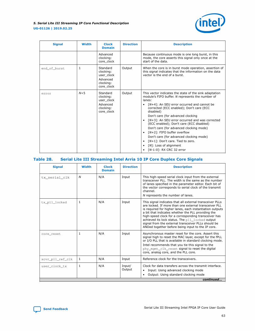
Signal Width ClockDomain
Direction Description
Advancedclocking:core_clock
Because continuous mode is one long burst, in thismode, the core asserts this signal only once at thestart of the data.
end_of_burst 1 Standardclocking:user_clockAdvancedclocking:core_clock
Output When the core is in burst mode operation, assertion ofthis signal indicates that the information on the datavector is the end of a burst.
error N+5 Standardclocking:user_clockAdvancedclocking:core_clock
Output This vector indicates the state of the sink adaptationmodule’s FIFO buffer. N represents the number oflanes:• [N+4]: An SEU error occurred and cannot be
corrected (ECC enabled); Don't care (ECCdisabled)Don't care (for advanced clocking
• [N+3]: An SEU error occurred and was corrected(ECC enabled); Don't care (ECC disabled)Don't care (for advanced clocking mode)
• [N+2]: FIFO buffer overflowDon't care (for advanced clocking mode)
• [N+1]: Don't care. Tied to zero.• [N]: Loss of alignment• [N-1:0]: RX CRC 32 error
Table 28. Serial Lite III Streaming Intel Arria 10 IP Core Duplex Core Signals
Signal Width ClockDomain
Direction Description
tx_serial_clk N N/A Input This high-speed serial clock input from the externaltransceiver PLL. The width is the same as the numberof lanes specified in the parameter editor. Each bit ofthe vector corresponds to serial clock of the transmitchannel.N represents the number of lanes.
tx_pll_locked 1 N/A Input This signal indicates that all external transceiver PLLsare locked. If more than one external transceiver PLLis required for higher lanes, each instantiation outputsa bit that indicates whether the PLL providing thehigh-speed clock for a corresponding transceiver hasachieved its lock status. The pll_locked outputsignal from the external transceiver PLLs should beANDed together before being input to the IP core.
core_reset 1 N/A Input Asynchronous master reset for the core. Assert thissignal high to reset the MAC layer, except for the fPLLor I/O PLL that is available in standard clocking mode.Intel recommends that you tie this signal to thephy_mgmt_clk_reset signal to reset the digitalcore, analog core, and the PLL core.
xcvr_pll_ref_clk 1 N/A Input Reference clock for the transceivers.
user_clock_tx 1 N/A Input/Output
Clock for data transfers across the transmit interface.• Input: Using advanced clocking mode• Output: Using standard clocking mode
continued...
5. Serial Lite III Streaming IP Core Functional Description
UG-01126 | 2019.02.25
Send Feedback Serial Lite III Streaming Intel FPGA IP Core User Guide
63
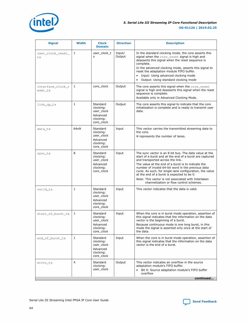
Signal Width ClockDomain
Direction Description
user_clock_reset_tx
1 user_clock_tx
Input/Output
In the standard clocking mode, the core asserts thissignal when the core_reset signal is high anddeasserts this signal when the reset sequence iscomplete.In the advanced clocking mode, asserts this signal toreset the adaptation module FIFO buffer.• Input: Using advanced clocking mode• Output: Using standard clocking mode
interface_clock_reset_tx
1 core_clock Output The core asserts this signal when the core_resetsignal is high and deasserts this signal when the resetsequence is complete.Available only in Advanced Clocking Mode.
link_up_tx 1 Standardclocking:user_clockAdvancedclocking:core_clock
Output The core asserts this signal to indicate that the coreinitialization is complete and is ready to transmit userdata.
data_tx 64xN Standardclocking:user_clockAdvancedclocking:core_clock
Input This vector carries the transmitted streaming data tothe core.N represents the number of lanes.
sync_tx 8 Standardclocking:user_clockAdvancedclocking:core_clock
Input The sync vector is an 8 bit bus. The data value at thestart of a burst and at the end of a burst are capturedand transported across the link.The value at the end of a burst is to indicate thenumber of invalid 64-bit word in the previous datacycle. As such, for single-lane configuration, the valueat the end of a burst is expected to be 0.Note: This vector is not associated with Interlaken
channelization or flow control schemes.
valid_tx 1 Standardclocking:user_clockAdvancedclocking:core_clock
Input This vector indicates that the data is valid.
start_of_burst_tx 1 Standardclocking:user_clockAdvancedclocking:core_clock
Input When the core is in burst mode operation, assertion ofthis signal indicates that the information on the datavector is the beginning of a burst.Because continuous mode is one long burst, in thismode the signal is asserted only once at the start ofthe data.
end_of_burst_tx 1 Standardclocking:user_clockAdvancedclocking:core_clock
Input When the core is in burst mode operation, assertion ofthis signal indicates that the information on the datavector is the end of a burst.
error_tx 4 Standardclocking:user_clock
Output This vector indicates an overflow in the sourceadaptation module’s FIFO buffer.• Bit 0: Source adaptation module’s FIFO buffer
overflow
continued...
5. Serial Lite III Streaming IP Core Functional Description
UG-01126 | 2019.02.25
Serial Lite III Streaming Intel FPGA IP Core User Guide Send Feedback
64
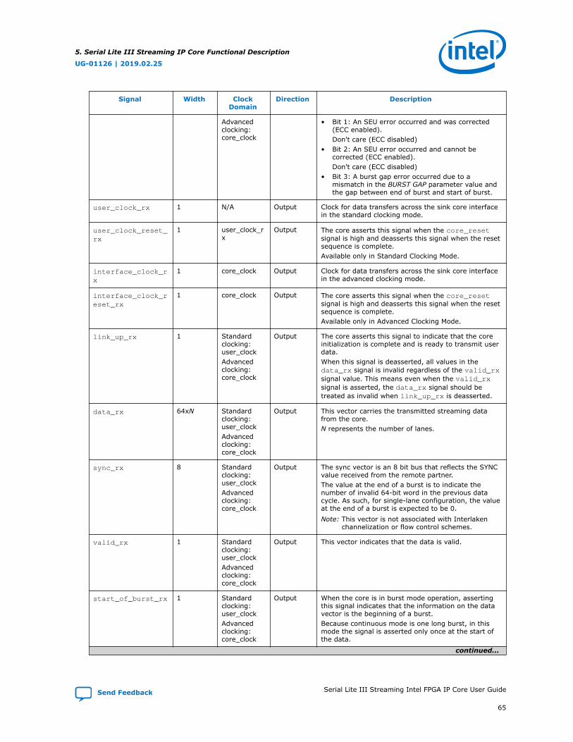
Signal Width ClockDomain
Direction Description
Advancedclocking:core_clock
• Bit 1: An SEU error occurred and was corrected(ECC enabled).Don't care (ECC disabled)
• Bit 2: An SEU error occurred and cannot becorrected (ECC enabled).Don't care (ECC disabled)
• Bit 3: A burst gap error occurred due to amismatch in the BURST GAP parameter value andthe gap between end of burst and start of burst.
user_clock_rx 1 N/A Output Clock for data transfers across the sink core interfacein the standard clocking mode.
user_clock_reset_rx
1 user_clock_rx
Output The core asserts this signal when the core_resetsignal is high and deasserts this signal when the resetsequence is complete.Available only in Standard Clocking Mode.
interface_clock_rx
1 core_clock Output Clock for data transfers across the sink core interfacein the advanced clocking mode.
interface_clock_reset_rx
1 core_clock Output The core asserts this signal when the core_resetsignal is high and deasserts this signal when the resetsequence is complete.Available only in Advanced Clocking Mode.
link_up_rx 1 Standardclocking:user_clockAdvancedclocking:core_clock
Output The core asserts this signal to indicate that the coreinitialization is complete and is ready to transmit userdata.When this signal is deasserted, all values in thedata_rx signal is invalid regardless of the valid_rxsignal value. This means even when the valid_rxsignal is asserted, the data_rx signal should betreated as invalid when link_up_rx is deasserted.
data_rx 64xN Standardclocking:user_clockAdvancedclocking:core_clock
Output This vector carries the transmitted streaming datafrom the core.N represents the number of lanes.
sync_rx 8 Standardclocking:user_clockAdvancedclocking:core_clock
Output The sync vector is an 8 bit bus that reflects the SYNCvalue received from the remote partner.The value at the end of a burst is to indicate thenumber of invalid 64-bit word in the previous datacycle. As such, for single-lane configuration, the valueat the end of a burst is expected to be 0.Note: This vector is not associated with Interlaken
channelization or flow control schemes.
valid_rx 1 Standardclocking:user_clockAdvancedclocking:core_clock
Output This vector indicates that the data is valid.
start_of_burst_rx 1 Standardclocking:user_clockAdvancedclocking:core_clock
Output When the core is in burst mode operation, assertingthis signal indicates that the information on the datavector is the beginning of a burst.Because continuous mode is one long burst, in thismode the signal is asserted only once at the start ofthe data.
continued...
5. Serial Lite III Streaming IP Core Functional Description
UG-01126 | 2019.02.25
Send Feedback Serial Lite III Streaming Intel FPGA IP Core User Guide
65

Signal Width ClockDomain
Direction Description
end_of_burst_rx 1 Standardclocking:user_clockAdvancedclocking:core_clock
Output When the core is in burst mode operation, assertingthis signal indicates that the information on the datavector is the end of a burst.You can optionally send an end of burst signal at theend of continuous mode.
error_rx N+5 Standardclocking:user_clockAdvancedclocking:core_clock
Output This vector indicates the state of the sink adaptationmodule’s FIFO buffer. N represents the number oflanes:• [N+4]: An SEU error occurred and cannot be
corrected (ECC enabled); Don't care (ECCdisabled)Don't care (for advanced clocking mode)
• [N+3]: An SEU error occurred and was corrected(ECC enabled); Don't care (ECC disabled)Don't care (for advanced clocking mode)
• [N+2]: FIFO buffer overflowDon't care (for advanced clocking mode)
• [N+1]: Don't care. Tied to zero.• [N]: Loss of alignment• [N-1:0]: RX CRC 32 error
crc_error_inject 1 Standardclocking:user_clock_txAdvancedclocking:core_clock_tx
Input This signal is used for CRC-32 error injection.
Table 29. Transceiver Native PHY Intel Arria 10 IP Core Signals (Interlaken Mode)
Signal Width Clock Domain Direction Description
phy_mgmt_clk 1 N/A Input Clock input for the Avalon-MM PHYmanagement interface within the Native PHYIP core. This signal also clocks the transceiverreconfiguration interface and sequences thereset state machine in the clock generationlogic.
phy_mgmt_clk_reset
1 phy_mgmt_clk Input Global reset signal that resets the entire IPincluding MAC, I/O PLL (available in standardclocking mode), and Native PHY IP core. Thissignal is active high and level sensitive.
phy_mgmt_addr 10 + log2N],N=number oflanes
phy_mgmt_clk Input Control and status register (CSR) address forIntel Arria 10 devices.The width depends on the number of lanes.The parameter editor determines the requiredwidth for you.You have to manually tie this extra bit (7).• phy_mgmt_addr[msb] = 1: for
Transceiver reconfiguration usage.• phy_mgmt_addr[msb] = 0: for soft CSR
(the transceiver reset and loopbackcontrol CSR)
continued...
5. Serial Lite III Streaming IP Core Functional Description
UG-01126 | 2019.02.25
Serial Lite III Streaming Intel FPGA IP Core User Guide Send Feedback
66

Signal Width Clock Domain Direction Description
phy_mgmt_writedata[31:0]
32 phy_mgmt_clk Input CSR write data.
phy_mgmt_readdata[31:0]
32 phy_mgmt_clk Output CSR read data.
phy_mgmt_write 1 phy_mgmt_clk Input Active high CSR write signal.
phy_mgmt_read 1 phy_mgmt_clk Input Active high CSR read signal.
phy_mgmt_waitrequest
1 phy_mgmt_clk Output CSR read or write request signal. Whenasserted, this signal indicates that the Avalon-MM slave interface is unable to respond to aread or write request.
reconfig_busy 1 phy_mgmt_clk Input For Intel Arria 10 devices, this signal ispresent but unused; tie this signal to 1’b0.
tx_serial_data N — Output The serial output data from the core.N represents the number of lanes.
rx_serial_data N — Input The serial input data to the core.N represents the number of lanes.
Related Information
Intel Arria 10 Transceiver PHY User GuideFor more information about the Intel Arria 10 Native PHY IP core.
5.9.3. Signals for Stratix V and Arria V GZ Devices
Table 30. Serial Lite III Streaming IP Core Source Core Signals for Stratix V and Arria VGZ Devices
Signal Width ClockDomain
Direction Description
core_reset 1 N/A Input Asynchronous master reset for the core. Assert thissignal high to reset the MAC layer, except for the fPLLthat is available in standard clocking mode.Intel recommends that you tie this signal to thephy_mgmt_clk_reset signal to reset the digitalcore, analog core, and the PLL core.
xcvr_pll_ref_clk 1 N/A Input This signal is the reference clock for the transceivers.
user_clock 1 N/A Input/Output
Clock for data transfers across the source coreinterface.• Input: Using advanced clocking mode• Output: Using standard clocking mode
user_clock_reset 1 user_clock Input/Output
In the standard clocking mode, the core asserts thissignal when the core_reset signal is high anddeasserts this signal when the reset sequence iscomplete.
continued...
(7) For more information about this bit, refer to the Interlaken PHY Registers table in the AlteraTransceiver PHY IP Core User Guide.
5. Serial Lite III Streaming IP Core Functional Description
UG-01126 | 2019.02.25
Send Feedback Serial Lite III Streaming Intel FPGA IP Core User Guide
67

Signal Width ClockDomain
Direction Description
In the advanced clocking mode, asserts this signal toreset the adaptation module FIFO buffer.• Input: Using advanced clocking mode• Output: Using standard clocking mode
link_up 1 user_clock Output The core asserts this signal to indicate that the coreinitialization is complete and is ready to transmit userdata.
data 64xN user_clock Input This vector carries the transmitted streaming data tothe core.N represents the number of lanes.
sync 8 user_clock Input The sync vector is an 8 bit bus. The data value at thestart of a burst and the end of a burst are capturedand transported across the link.The value at the end of a burst is to indicate thenumber of invalid 64-bit word in the previous datacycle. As such, for single-lane configuration, the valueat the end of a burst is expected to be 0.Note: This vector is not associated with Interlaken
channelization or flow control schemes.
valid 1 user_clock Input This single bit signal indicates that the transmittedstreaming data is valid.
start_of_burst 1 user_clock Input When the core is in burst mode operation, assertingthis signal indicates that the information on the datavector is the beginning of a burst.Because continuous mode is one long burst, in thismode the signal is asserted only once at the start ofthe data.
end_of_burst 1 user_clock Input When the core is in burst mode operation, assertingthis signal indicates that the information on the datavector is the end of a burst.You can optionally send an end of burst signal at theend of continuous mode.
error 4 user_clock Output This vector indicates an error or overflow in the sourceadaptation module’s FIFO buffer.• Bit 0: Source adaptation module’s FIFO buffer
overflow• Bit 1: An SEU error occurred and was corrected
(ECC enabled)Don't care (ECC disabled)
• Bit 2: An SEU error occurred and cannot becorrected (ECC enabled)Don't care (ECC disabled)
• Bit 3: A burst gap error occurred due to amismatch in the BURST GAP parameter value andthe gap between end of burst and start of burst.
crc_error_inject 1 user_clock Input This signal forces CRC-32 errors when CRC-32 errorinjection is enabled in the transceiver channels. TheCRC-32 error injection is enabled via the transceiverreconfiguration controller.
5. Serial Lite III Streaming IP Core Functional Description
UG-01126 | 2019.02.25
Serial Lite III Streaming Intel FPGA IP Core User Guide Send Feedback
68

Table 31. Serial Lite III Streaming IP Core Sink Core Signals for Stratix V and Arria VGZ Devices
Signal Width ClockDomain
Direction Description
core_reset 1 N/A Input Asynchronous master reset for the core. Assert thissignal high to reset the MAC layer, except for the fPLLthat is available in standard clocking mode.Intel recommends that you tie this signal to thephy_mgmt_clk_reset signal to reset the digitalcore, analog core, and the PLL core.
xcvr_pll_ref_clk 1 N/A Input Reference clock for the transceivers.
user_clock 1 N/A Output Clock for data transfers across the sink core interfacein the standard clocking mode.
user_clock_reset 1 user_clock Output The core asserts this signal when the core_resetsignal is high and deasserts this signal when the resetsequence is complete in the standard clocking mode.
interface_clock 1 core_clock Output Clock for data transfer across the sink core interfacein the advanced clocking mode.
interface_clock_reset
1 core_clock Output The core asserts this signal when the core_resetsignal is high and deasserts this signal when the resetsequence is complete in the advanced clocking mode.
link_up 1 Standardclocking:user_clockAdvancedclocking:core_clock
Output The core asserts this signal to indicate that the coreinitialization is complete and is ready to transmit userdata.When this signal is deasserted, all values in thedata_rx signal is invalid regardless of the valid_rxsignal value. This means even when the valid_rxsignal is asserted, the data_rx signal should betreated as invalid when link_up_rx is deasserted.
data 64xN Standardclocking:user_clockAdvancedclocking:core_clock
Output This vector carries the transmitted streaming datafrom the core.N represents the number of lanes.
sync 8 Standardclocking:user_clockAdvancedclocking:core_clock
Output The sync vector is an 8 bit bus that reflects the SYNCvalue received from the remote partner.The value at the end of a burst is to indicate thenumber of invalid 64-bit word in the previous datacycle. As such, for single-lane configuration, the valueat the end of a burst is expected to be 0.Note: This vector is not associated with Interlaken
channelization or flow control schemes.
valid 1 Standardclocking:user_clockAdvancedclocking:core_clock
Output This single bit signal indicates that the data is valid.
start_of_burst 1 Standardclocking:user_clock
Output When the core is in burst mode operation, assertion ofthis signal indicates that the information on the datavector is the beginning of a burst.
continued...
5. Serial Lite III Streaming IP Core Functional Description
UG-01126 | 2019.02.25
Send Feedback Serial Lite III Streaming Intel FPGA IP Core User Guide
69

Signal Width ClockDomain
Direction Description
Advancedclocking:core_clock
Because continuous mode is one long burst, in thismode, the core asserts this signal only once at thestart of the data.
end_of_burst 1 Standardclocking:user_clockAdvancedclocking:core_clock
Output When the core is in burst mode operation, assertion ofthis signal indicates that the information on the datavector is the end of a burst.
error N+5 Standardclocking:user_clockAdvancedclocking:core_clock
Output This vector indicates the state of the sink adaptationmodule’s FIFO buffer. N represents the number oflanes:• [N+4]: An SEU error occurred and cannot be
corrected (ECC enabled); Don't care (ECCdisabled)Don't care (for advanced clocking mode)
• [N+3]: An SEU error occurred and was corrected(ECC enabled); Don't care (ECC disabled)Don't care (for advanced clocking mode)
• [N+2]: FIFO buffer overflowDon't care (for advanced clocking mode)
• [N+1]: Don't care. Tied to zero.• [N]: Loss of alignment• [N-1:0]: RX CRC 32 error
Table 32. Serial Lite III Streaming IP Core Duplex Core Signals for Stratix V and Arria VGZ Devices
Signal Width ClockDomain
Direction Description
core_reset 1 N/A Input Asynchronous master reset for the core. Assert thissignal high to reset the MAC layer, except for the fPLLthat is available in standard clocking mode.Intel recommends that you tie this signal to thephy_mgmt_clk_reset signal to reset the digitalcore, analog core, and the PLL core.
xcvr_pll_ref_clk 1 N/A Input Reference clock for the transceivers.
user_clock_tx 1 N/A Input/Output
Clock for data transfers across the transmit interface.• Input: Using advanced clocking mode• Output: Using standard clocking mode
user_clock_reset_tx
1 user_clock_tx
Input/Output
In the standard clocking mode, the core asserts thissignal when the core_reset signal is high anddeasserts this signal when the reset sequence iscomplete.In the advanced clocking mode, asserts this signal toreset the adaptation module FIFO buffer.• Input: Using advanced clocking mode• Output: Using standard clocking mode
interface_clock_reset_tx
1 core_clock Output In the advanced clocking mode, the core asserts thissignal when the core_reset signal is high anddeasserts this signal when the reset sequence iscomplete.
continued...
5. Serial Lite III Streaming IP Core Functional Description
UG-01126 | 2019.02.25
Serial Lite III Streaming Intel FPGA IP Core User Guide Send Feedback
70

Signal Width ClockDomain
Direction Description
link_up_tx 1 Standardclocking:user_clockAdvancedclocking:core_clock
Output The core asserts this signal to indicate that the coreinitialization is complete and is ready to transmit userdata.
data_tx 64xN Standardclocking:user_clockAdvancedclocking:core_clock
Input This vector carries the transmitted streaming data tothe core.N represents the number of lanes.
sync_tx 8 Standardclocking:user_clockAdvancedclocking:core_clock
Input The sync vector is an 8 bit bus. The data value at thestart of a burst and at the end of a burst are capturedand transported across the link.The value at the end of a burst is to indicate thenumber of invalid 64-bit word in the previous datacycle. As such, for single-lane configuration, the valueat the end of a burst is expected to be 0.Note: This vector is not associated with Interlaken
channelization or flow control schemes.
valid_tx 1 Standardclocking:user_clockAdvancedclocking:core_clock
Input This vector indicates that the data is valid.
start_of_burst_tx 1 Standardclocking:user_clockAdvancedclocking:core_clock
Input When the core is in burst mode operation, assertion ofthis signal indicates that the information on the datavector is the beginning of a burst.Because continuous mode is one long burst, in thismode the signal is asserted only once at the start ofthe data.
end_of_burst_tx 1 Standardclocking:user_clockAdvancedclocking:core_clock
Input When the core is in burst mode operation, assertion ofthis signal indicates that the information on the datavector is the end of a burst.
error_tx 4 Standardclocking:user_clockAdvancedclocking:core_clock
Output This vector indicates an overflow in the sourceadaptation module’s FIFO buffer.• Bit 0: Source adaptation module’s FIFO buffer
overflow• Bit 1: An SEU error occurred and was corrected
(ECC enabled).Don't care (ECC disabled)
• Bit 2: An SEU error occurred and cannot becorrected (ECC enabled).Don't care (ECC disabled)
• Bit 3: A burst gap error occurred due to amismatch in the BURST GAP parameter value andthe gap between end of burst and start of burst.
user_clock_rx 1 N/A Output Clock for data transfers across the sink core interfacein the standard clocking mode.
continued...
5. Serial Lite III Streaming IP Core Functional Description
UG-01126 | 2019.02.25
Send Feedback Serial Lite III Streaming Intel FPGA IP Core User Guide
71
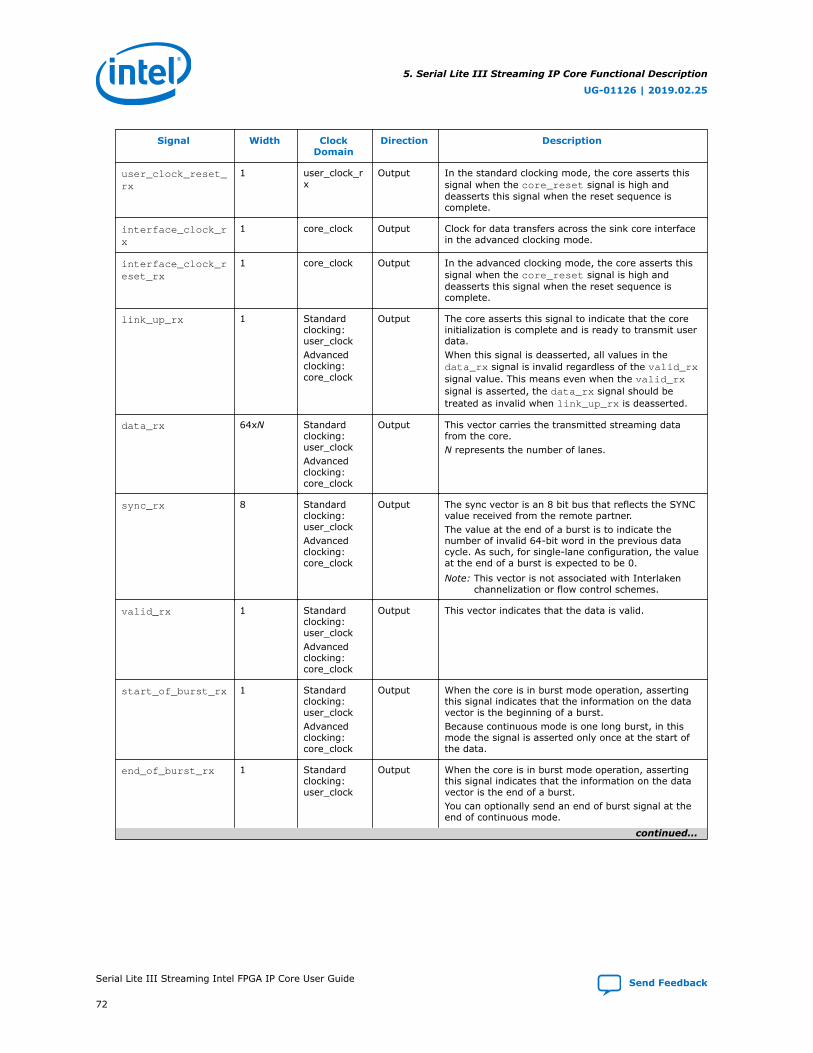
Signal Width ClockDomain
Direction Description
user_clock_reset_rx
1 user_clock_rx
Output In the standard clocking mode, the core asserts thissignal when the core_reset signal is high anddeasserts this signal when the reset sequence iscomplete.
interface_clock_rx
1 core_clock Output Clock for data transfers across the sink core interfacein the advanced clocking mode.
interface_clock_reset_rx
1 core_clock Output In the advanced clocking mode, the core asserts thissignal when the core_reset signal is high anddeasserts this signal when the reset sequence iscomplete.
link_up_rx 1 Standardclocking:user_clockAdvancedclocking:core_clock
Output The core asserts this signal to indicate that the coreinitialization is complete and is ready to transmit userdata.When this signal is deasserted, all values in thedata_rx signal is invalid regardless of the valid_rxsignal value. This means even when the valid_rxsignal is asserted, the data_rx signal should betreated as invalid when link_up_rx is deasserted.
data_rx 64xN Standardclocking:user_clockAdvancedclocking:core_clock
Output This vector carries the transmitted streaming datafrom the core.N represents the number of lanes.
sync_rx 8 Standardclocking:user_clockAdvancedclocking:core_clock
Output The sync vector is an 8 bit bus that reflects the SYNCvalue received from the remote partner.The value at the end of a burst is to indicate thenumber of invalid 64-bit word in the previous datacycle. As such, for single-lane configuration, the valueat the end of a burst is expected to be 0.Note: This vector is not associated with Interlaken
channelization or flow control schemes.
valid_rx 1 Standardclocking:user_clockAdvancedclocking:core_clock
Output This vector indicates that the data is valid.
start_of_burst_rx 1 Standardclocking:user_clockAdvancedclocking:core_clock
Output When the core is in burst mode operation, assertingthis signal indicates that the information on the datavector is the beginning of a burst.Because continuous mode is one long burst, in thismode the signal is asserted only once at the start ofthe data.
end_of_burst_rx 1 Standardclocking:user_clock
Output When the core is in burst mode operation, assertingthis signal indicates that the information on the datavector is the end of a burst.You can optionally send an end of burst signal at theend of continuous mode.
continued...
5. Serial Lite III Streaming IP Core Functional Description
UG-01126 | 2019.02.25
Serial Lite III Streaming Intel FPGA IP Core User Guide Send Feedback
72
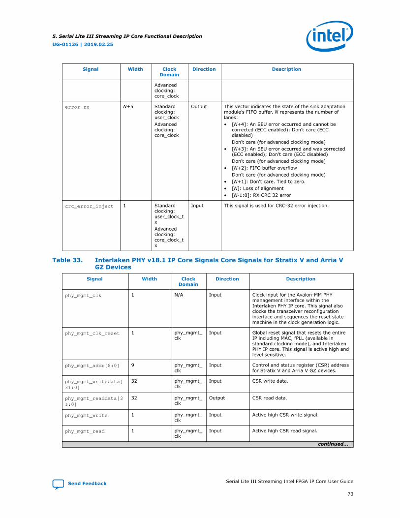
Signal Width ClockDomain
Direction Description
Advancedclocking:core_clock
error_rx N+5 Standardclocking:user_clockAdvancedclocking:core_clock
Output This vector indicates the state of the sink adaptationmodule’s FIFO buffer. N represents the number oflanes:• [N+4]: An SEU error occurred and cannot be
corrected (ECC enabled); Don't care (ECCdisabled)Don't care (for advanced clocking mode)
• [N+3]: An SEU error occurred and was corrected(ECC enabled); Don't care (ECC disabled)Don't care (for advanced clocking mode)
• [N+2]: FIFO buffer overflowDon't care (for advanced clocking mode)
• [N+1]: Don't care. Tied to zero.• [N]: Loss of alignment• [N-1:0]: RX CRC 32 error
crc_error_inject 1 Standardclocking:user_clock_txAdvancedclocking:core_clock_tx
Input This signal is used for CRC-32 error injection.
Table 33. Interlaken PHY v18.1 IP Core Signals Core Signals for Stratix V and Arria VGZ Devices
Signal Width ClockDomain
Direction Description
phy_mgmt_clk 1 N/A Input Clock input for the Avalon-MM PHYmanagement interface within theInterlaken PHY IP core. This signal alsoclocks the transceiver reconfigurationinterface and sequences the reset statemachine in the clock generation logic.
phy_mgmt_clk_reset 1 phy_mgmt_clk
Input Global reset signal that resets the entireIP including MAC, fPLL (available instandard clocking mode), and InterlakenPHY IP core. This signal is active high andlevel sensitive.
phy_mgmt_addr[8:0] 9 phy_mgmt_clk
Input Control and status register (CSR) addressfor Stratix V and Arria V GZ devices.
phy_mgmt_writedata[31:0]
32 phy_mgmt_clk
Input CSR write data.
phy_mgmt_readdata[31:0]
32 phy_mgmt_clk
Output CSR read data.
phy_mgmt_write 1 phy_mgmt_clk
Input Active high CSR write signal.
phy_mgmt_read 1 phy_mgmt_clk
Input Active high CSR read signal.
continued...
5. Serial Lite III Streaming IP Core Functional Description
UG-01126 | 2019.02.25
Send Feedback Serial Lite III Streaming Intel FPGA IP Core User Guide
73

Signal Width ClockDomain
Direction Description
phy_mgmt_waitrequest
1 phy_mgmt_clk
Output CSR read or write request signal. Whenasserted, this signal indicates that theAvalon-MM slave interface is unable torespond to a read or write request.
reconfig_busy 1 phy_mgmt_clk
Input For Stratix V and Arria V GZ devices,when asserted, this signal indicates that areconfiguration operation is in progressand no further reconfiguration operationsshould be performed. You can monitorthis signal to determine the status of theTransceiver Reconfiguration Controller.
reconfig_to_xcvr • Source core:140xN
• Sink core:70xN
• Duplex core:140xN
phy_mgmt_clk
Input Dynamic reconfiguration input for theInterlaken PHY IP.N represents the number of lanes.
reconfig_from_ xcvr • Source core:92xN
• Sink core:46xN
• Duplex core:92xN
phy_mgmt_clk
Output Dynamic reconfiguration output for theInterlaken PHY IP.N represents the number of lanes.
tx_serial_data N — Output The serial output data from the core.N represents the number of lanes.
rx_serial_data N — Input The serial input data to the core.N represents the number of lanes.
Related Information
• V-Series Transceiver PHY IP Core User Guide
• Loopback ModesMore information about pre- and post-CDR RX to TX serial loopback modes inthe Transceiver Reconfiguration Controller IP Core.
5.10. Accessing Configuration and Status Registers
The Avalon-MM PHY management block within the Interlaken PHY IP core or NativePHY IP core includes master and slave interfaces. This component acts as a bridge. Ittransfers commands received on its Avalon-MM slave interface to its Avalon-MM port.This interface manages PCS and PMA modules, resets, error handling, and serialloopback controls. Refer to Configuration and Status Registers on page 95 for moreinformation of registers that you can access using the Avalon-MM PHY managementinterface using word addresses and a 32-bit embedded processor. A single addressspace provides access to all registers.
5. Serial Lite III Streaming IP Core Functional Description
UG-01126 | 2019.02.25
Serial Lite III Streaming Intel FPGA IP Core User Guide Send Feedback
74
6. Serial Lite III Streaming IP Core Clocking GuidelinesThis section describes the Serial Lite III Streaming IP core clocking architecture andusage models targeting streaming applications.
The Serial Lite III Streaming IP core has two clocking options to support a variety ofstreaming applications:
• Standard Clocking Mode (SCM):
— In this clocking mode, there is no PPM difference (mesochronous system) inboth source and sink cores for Intel Arria 10, Stratix V, and Arria V devices.The user interface clock and IP core clock are generated from the same clocksource in both source and sink cores.
— For Intel Stratix 10 devices, this clocking mode is the same as advancedclocking mode for source core. For sink core, a user interface clock is requiredto drive the adaptation module in the core. To design a mesochronous system,Intel recommends to use the same clock source for transceiver input clock inboth source and sink cores.
• Advanced Clocking Mode (ACM):
— In this clocking mode, for source core, user is required to manage any PPMdifference between the user interface logic domain and the transceiver clockdomain by throttling the data input or use the same clock source for userinterface and transceiver clock domains. The IP core does not support any PPMtolerance between the user interface domain and the transceiver clockdomain. For sink core, there is no PPM differences because user is expected touse the recovered clock for user interface logic.
The following sections describe the clocking architectures for Intel Stratix 10, IntelArria 10, Stratix V, and Arria V GZ devices.
6.1. Standard Clocking Mode
6.1.1. Standard Clocking Mode in Serial Lite III Streaming Intel FPGA IPCore (Intel Stratix 10 Devices)
In this mode, you are required to provide a user clock to drive the user interface forboth source and sink core, and specify the user clock frequency through theparameter editor. The Intel Quartus Prime software then automatically determines therequired transceiver reference clock from the L-Tile/H-Tile/E-Tile Transceiver NativePHY IP core, provide a list of values for selection and generate a reference clocksignal. This reference clock connects to a global clock network that generates a coreclock for IP core.
Figure below shows the source and sink variant clocking structure for standardclocking mode in Intel Stratix 10 devices.
UG-01126 | 2019.02.25
Send Feedback
Intel Corporation. All rights reserved. Intel, the Intel logo, Altera, Arria, Cyclone, Enpirion, MAX, Nios, Quartusand Stratix words and logos are trademarks of Intel Corporation or its subsidiaries in the U.S. and/or othercountries. Intel warrants performance of its FPGA and semiconductor products to current specifications inaccordance with Intel's standard warranty, but reserves the right to make changes to any products and servicesat any time without notice. Intel assumes no responsibility or liability arising out of the application or use of anyinformation, product, or service described herein except as expressly agreed to in writing by Intel. Intelcustomers are advised to obtain the latest version of device specifications before relying on any publishedinformation and before placing orders for products or services.*Other names and brands may be claimed as the property of others.
ISO9001:2015Registered
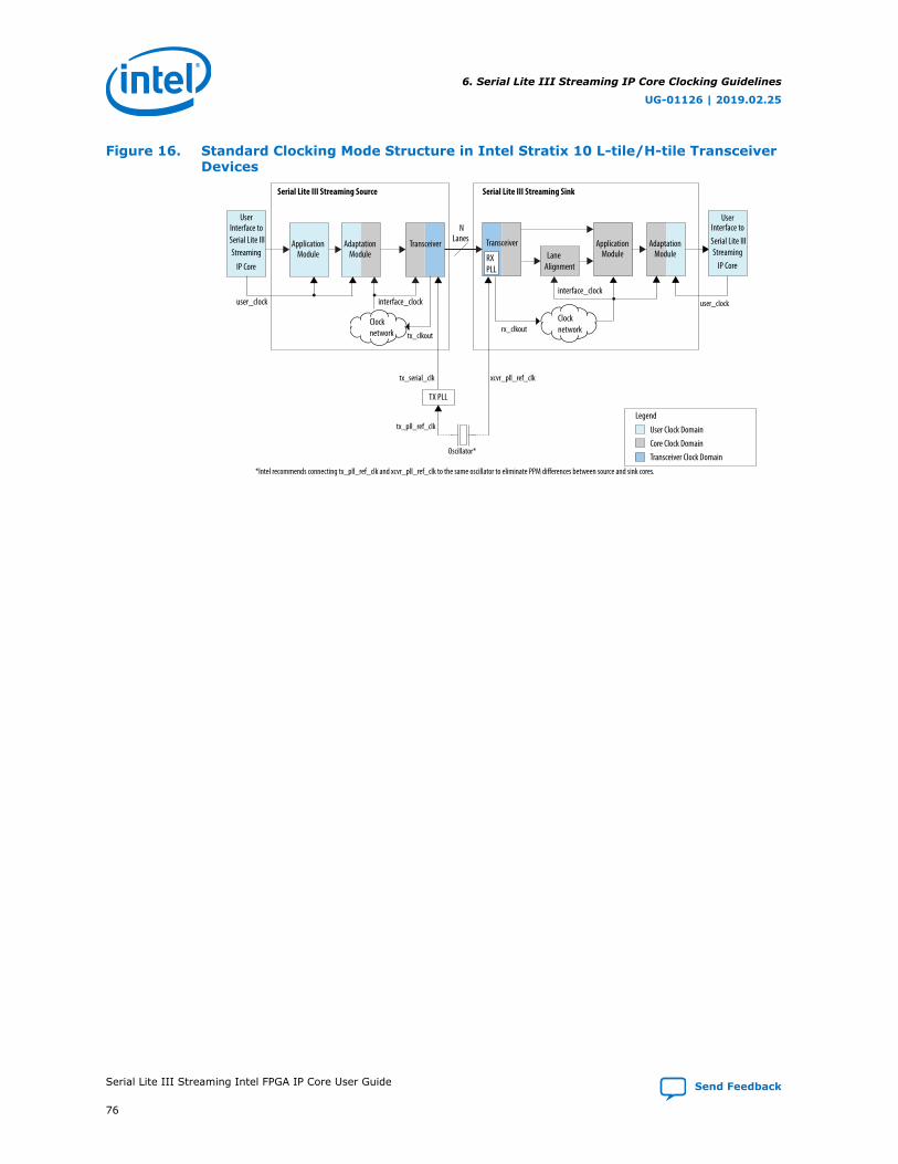
Figure 16. Standard Clocking Mode Structure in Intel Stratix 10 L-tile/H-tile TransceiverDevices
ApplicationModule
Transceiver
Serial Lite III Streaming Source
AdaptationModule
user_clock
ApplicationModule
Transceiver
Serial Lite III Streaming Sink
AdaptationModuleLane
Alignment
NLanes
User Clock Domain
Legend
Core Clock DomainTransceiver Clock Domain
Clock network
TX PLL
UserInterface toSerial Lite IIIStreaming
IP Core
UserInterface toSerial Lite IIIStreaming
IP Core
tx_clkout
tx_serial_clk
tx_pll_ref_clk
xcvr_pll_ref_clk
rx_clkout
user_clockinterface_clockinterface_clock
Clock network
Oscillator*
*Intel recommends connecting tx_pll_ref_clk and xcvr_pll_ref_clk to the same oscillator to eliminate PPM differences between source and sink cores.
RXPLL
6. Serial Lite III Streaming IP Core Clocking Guidelines
UG-01126 | 2019.02.25
Serial Lite III Streaming Intel FPGA IP Core User Guide Send Feedback
76

Figure 17. Standard Clocking Mode Structure in Intel Stratix 10 E-tile TransceiverDevices
ApplicationModule
Serial Lite III Streaming Duplex
AdaptationModule
user_clock
Application
ModuleAdaptation
Module LaneAlignment
User Clock Domain
Legend
Core Clock DomainTransceiver Clock Domain
UserInterface toSerial Lite IIIStreaming
IP Core
UserInterface toSerial Lite IIIStreaming
IP Core
xcvr_pll_ref_clk
rx_clkout
user_clockinterface_clock
Clock network
NLanes
NLanes
Clock network
tx_clkout
interface_clock
TX/RXTransceiver
Table 34. Intel Stratix 10 Clocks in Standard Clocking Mode
Clock Name Description
Source
user_clock User-defined. This clock is determined by the required throughput of the userapplication. For example, if the user interface is 384-bits wide (6 lanes × 64 bit/lane) and the required throughput is 120 Gbps, the user_clock frequency is312.5 MHz. This is an input clock provided by the user to the IP and should beused to clock the user interface.Note: Use the same clock source as the tx_pll_ref_clk for zero clock PPM
implementation.
tx_serial_clk This clock should toggle at one-half the data rate of the transceiver lane. Whenyou enter the user_clock frequency in the IP parameter editor, the per lanedata rate is calculated. Use that value and divided it by two to determine thetx_serial_clk. You are required to instantiate the TX PLL, as shown in thefigure above. In the Serial Lite III Streaming design example, an example of theTX PLL (ATX PLL) is generated with the IP core and is configured with therequired reference clock and tx_serial_clk.Note: This signal is not available when you select E-Tile as as the transceiver
tile.
continued...
6. Serial Lite III Streaming IP Core Clocking Guidelines
UG-01126 | 2019.02.25
Send Feedback Serial Lite III Streaming Intel FPGA IP Core User Guide
77
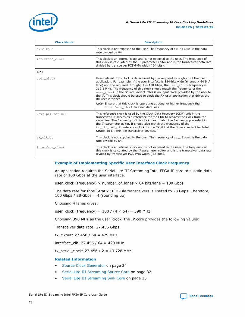
Clock Name Description
tx_clkout This clock is not exposed to the user. The frequency of tx_clkout is the datarate divided by 64.
interface_clock This clock is an internal clock and is not exposed to the user. The frequency ofthis clock is calculated by the IP parameter editor and is the transceiver data ratedivided by transceiver PCS-PMA width ( 64 bits).
Sink
user_clock User-defined. This clock is determined by the required throughput of the userapplication. For example, if the user interface is 384-bits wide (6 lanes × 64 bit/lane) and the required throughput is 120 Gbps, the user_clock frequency is312.5 MHz. The frequency of this clock should match the frequency of theuser_clock in the Source variant. This is an input clock provided by the user tothe IP. This clock should be used to clock the RX user application that drives theRX user interface.Note: Ensure that this clock is operating at equal or higher frequency than
interface_clock to avoid data loss.
xcvr_pll_ref_clk This reference clock is used by the Clock Data Recovery (CDR) unit in thetransceiver. It serves as a reference for the CDR to recover the clock from theserial line. The frequency of this clock must match the frequency you select inthe IP parameter editor. It should also match the frequency of thetx_pll_ref_clk reference clock for the TX PLL at the Source variant for IntelStratix 10 L-tile/H-tile transceiver devices.
rx_clkout This clock is not exposed to the user. The frequency of rx_clkout is the datarate divided by 64.
interface_clock This clock is an internal clock and is not exposed to the user. The frequency ofthis clock is calculated by the IP parameter editor and is the transceiver data ratedivided by transceiver PCS-PMA width ( 64 bits).
Example of Implementing Specific User Interface Clock Frequency
An application requires the Serial Lite III Streaming Intel FPGA IP core to sustain datarate of 100 Gbps at the user interface.
user_clock (frequency) × number_of_lanes × 64 bits/lane = 100 Gbps
The data rate for Intel Stratix 10 H-Tile transceivers is limited to 28 Gbps. Therefore,100 Gbps / 28 Gbps = 4 (rounding up)
Choosing 4 lanes gives:
user_clock (frequency) = 100 / (4 × 64) = 390 MHz
Choosing 390 MHz as the user_clock, the IP core provides the following values:
Transceiver data rate: 27.456 Gbps
tx_clkout: 27.456 / 64 = 429 MHz
interface_clk: 27.456 / 64 = 429 MHz
tx_serial_clock: 27.456 / 2 = 13.728 MHz
Related Information
• Source Clock Generator on page 34
• Serial Lite III Streaming Source Core on page 32
• Serial Lite III Streaming Sink Core on page 35
6. Serial Lite III Streaming IP Core Clocking Guidelines
UG-01126 | 2019.02.25
Serial Lite III Streaming Intel FPGA IP Core User Guide Send Feedback
78
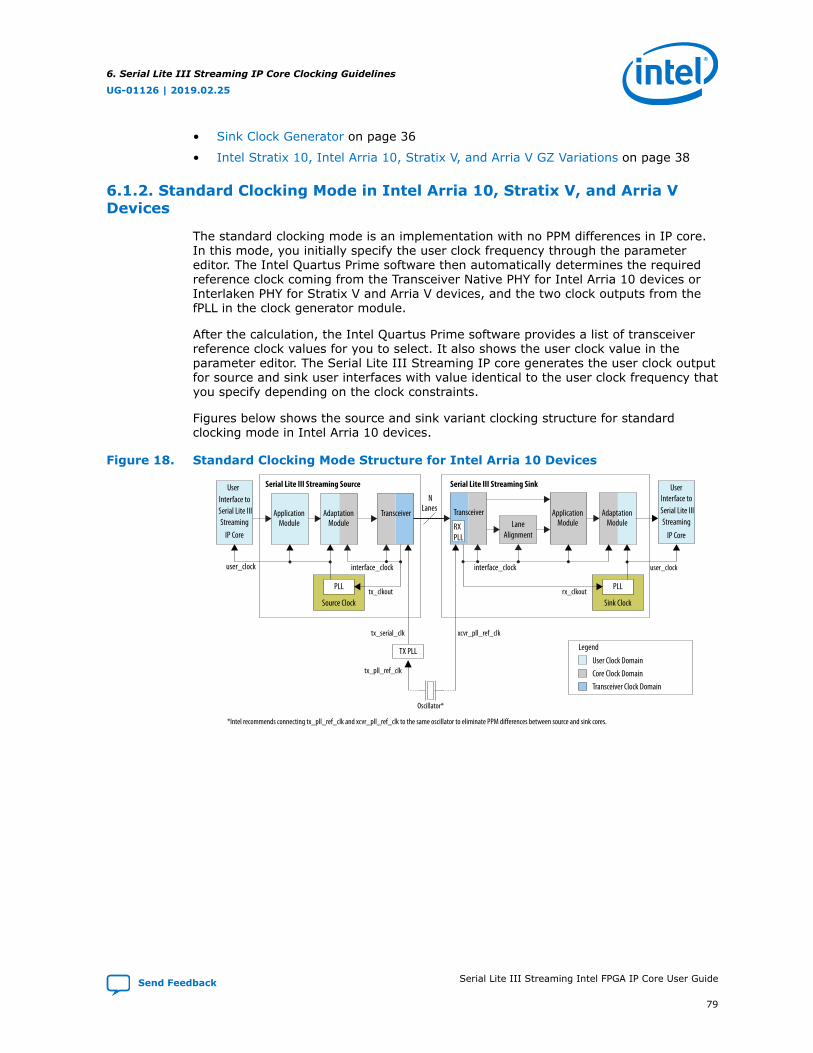
• Sink Clock Generator on page 36
• Intel Stratix 10, Intel Arria 10, Stratix V, and Arria V GZ Variations on page 38
6.1.2. Standard Clocking Mode in Intel Arria 10, Stratix V, and Arria VDevices
The standard clocking mode is an implementation with no PPM differences in IP core.In this mode, you initially specify the user clock frequency through the parametereditor. The Intel Quartus Prime software then automatically determines the requiredreference clock coming from the Transceiver Native PHY for Intel Arria 10 devices orInterlaken PHY for Stratix V and Arria V devices, and the two clock outputs from thefPLL in the clock generator module.
After the calculation, the Intel Quartus Prime software provides a list of transceiverreference clock values for you to select. It also shows the user clock value in theparameter editor. The Serial Lite III Streaming IP core generates the user clock outputfor source and sink user interfaces with value identical to the user clock frequency thatyou specify depending on the clock constraints.
Figures below shows the source and sink variant clocking structure for standardclocking mode in Intel Arria 10 devices.
Figure 18. Standard Clocking Mode Structure for Intel Arria 10 Devices
ApplicationModule
Transceiver
Serial Lite III Streaming Source
AdaptationModule
user_clock interface_clock
ApplicationModule
Transceiver
Serial Lite III Streaming Sink
AdaptationModule
interface_clock
LaneAlignment
NLanes
User Clock Domain
Legend
Core Clock DomainTransceiver Clock Domain
PLL
Source Clock
TX PLL
UserInterface toSerial Lite IIIStreaming
IP Core
UserInterface toSerial Lite IIIStreaming
IP Core
tx_clkout
tx_serial_clk
tx_pll_ref_clk
PLL
Sink Clock
xcvr_pll_ref_clk
rx_clkout
user_clock
Oscillator*
*Intel recommends connecting tx_pll_ref_clk and xcvr_pll_ref_clk to the same oscillator to eliminate PPM differences between source and sink cores.
RXPLL
6. Serial Lite III Streaming IP Core Clocking Guidelines
UG-01126 | 2019.02.25
Send Feedback Serial Lite III Streaming Intel FPGA IP Core User Guide
79
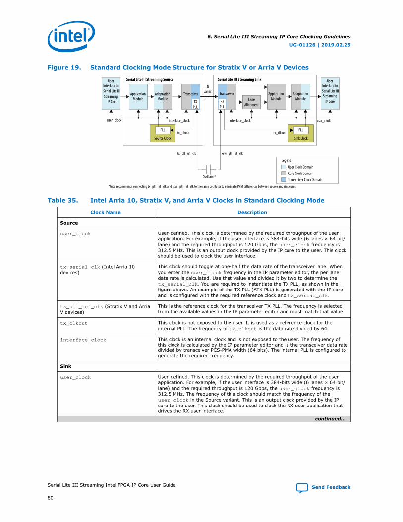
Figure 19. Standard Clocking Mode Structure for Stratix V or Arria V Devices
ApplicationModule
Transceiver
Serial Lite III Streaming Source
AdaptationModule
user_clock interface_clock
ApplicationModule
Transceiver
Serial Lite III Streaming Sink
AdaptationModule
interface_clock
LaneAlignment
NLanes
User Clock Domain
Legend
Core Clock DomainTransceiver Clock Domain
PLL
Source Clock
TXPLL
UserInterface toSerial Lite IIIStreaming
IP Core
UserInterface toSerial Lite IIIStreaming
IP Core
tx_clkout
tx_pll_ref_clk
PLL
Sink Clock
xcvr_pll_ref_clk
rx_clkout
user_clock
Oscillator*
*Intel recommends connecting tx_pll_ref_clk and xcvr_pll_ref_clk to the same oscillator to eliminate PPM differences between source and sink cores.
RXPLL
Table 35. Intel Arria 10, Stratix V, and Arria V Clocks in Standard Clocking Mode
Clock Name Description
Source
user_clock User-defined. This clock is determined by the required throughput of the userapplication. For example, if the user interface is 384-bits wide (6 lanes × 64 bit/lane) and the required throughput is 120 Gbps, the user_clock frequency is312.5 MHz. This is an output clock provided by the IP core to the user. This clockshould be used to clock the user interface.
tx_serial_clk (Intel Arria 10devices)
This clock should toggle at one-half the data rate of the transceiver lane. Whenyou enter the user_clock frequency in the IP parameter editor, the per lanedata rate is calculated. Use that value and divided it by two to determine thetx_serial_clk. You are required to instantiate the TX PLL, as shown in thefigure above. An example of the TX PLL (ATX PLL) is generated with the IP coreand is configured with the required reference clock and tx_serial_clk.
tx_pll_ref_clk (Stratix V and ArriaV devices)
This is the reference clock for the transceiver TX PLL. The frequency is selectedfrom the available values in the IP parameter editor and must match that value.
tx_clkout This clock is not exposed to the user. It is used as a reference clock for theinternal PLL. The frequency of tx_clkout is the data rate divided by 64.
interface_clock This clock is an internal clock and is not exposed to the user. The frequency ofthis clock is calculated by the IP parameter editor and is the transceiver data ratedivided by transceiver PCS-PMA width (64 bits). The internal PLL is configured togenerate the required frequency.
Sink
user_clock User-defined. This clock is determined by the required throughput of the userapplication. For example, if the user interface is 384-bits wide (6 lanes × 64 bit/lane) and the required throughput is 120 Gbps, the user_clock frequency is312.5 MHz. The frequency of this clock should match the frequency of theuser_clock in the Source variant. This is an output clock provided by the IPcore to the user. This clock should be used to clock the RX user application thatdrives the RX user interface.
continued...
6. Serial Lite III Streaming IP Core Clocking Guidelines
UG-01126 | 2019.02.25
Serial Lite III Streaming Intel FPGA IP Core User Guide Send Feedback
80
Clock Name Description
xcvr_pll_ref_clk This reference clock is used by the Clock Data Recovery (CDR) unit in thetransceiver. It serves as a reference for the CDR to recover the clock from theserial line. The frequency of this clock must match the frequency you select inthe IP parameter editor. It should also match the frequency of thetx_pll_ref_clk reference clock for the TX PLL at the Source variant.
rx_clkout This clock is not exposed to the user. It is used as a reference clock for theinternal PLL in the Sink. The frequency of rx_clkout is the data rate divided by64.
interface_clock This clock is an internal clock and is not exposed to the user. The frequency ofthis clock is calculated by the IP parameter editor and is the transceiver data ratedivided by transceiver PCS-PMA width (64 bits). The internal PLL is configured togenerate the required frequency.
Example of Implementing Specific User Interface Clock Frequency
An application requires the Serial Lite III Streaming Intel Arria 10 FPGA IP core tosustain a frequency of 300 Gbps at the user interface.
user_clock (frequency) × number_of_lanes × 64 bits/lane = 300 Gbps
The data rate for Intel Arria 10 GX transceivers is limited to 17.4 Gbps. Therefore, 300Gbps / 17.4 Gbps = 18 (rounding up)
Choosing 18 lanes gives:
user_clock (frequency) = 300 / (18 × 64) = 260.42 MHz
A value of 260.40 MHz is out of the supported range for the user_clock frequency.Therefore, you need to add one more lane.
user_clock (frequency) = 300 / (19 × 64) = 246.71 MHz
Choosing 246.71 MHz as the user_clock, the IP core provides the following values:
Transceiver data rate: 17.368 Gbps
tx_clkout: 17.368 / 64 = 271.375 MHz
interface_clk: 17.368 / 64 = 271.375 MHz
tx_serial_clock: 17.368 / 2 = 8684 MHz
Related Information
• Source Clock Generator on page 34
• Serial Lite III Streaming Source Core on page 32
• Serial Lite III Streaming Sink Core on page 35
• Sink Clock Generator on page 36
• Intel Stratix 10, Intel Arria 10, Stratix V, and Arria V GZ Variations on page 38
6. Serial Lite III Streaming IP Core Clocking Guidelines
UG-01126 | 2019.02.25
Send Feedback Serial Lite III Streaming Intel FPGA IP Core User Guide
81

6.2. Advanced Clocking Mode
6.2.1. Advanced Clocking Mode Structure for Serial Lite III StreamingIntel FPGA IP Core (Intel Stratix 10 Devices)
In this mode, you must specify the user clock frequency through the Serial Lite IIIStreaming Intel FPGA IP core parameter editor. Based on the user clock frequencyvalue, the Intel Quartus Prime software automatically calculates the lane rate and coreclock.
The parameter editor provides guidance in selecting a source user clock frequencythat meets the transceiver data rate constraints. For more information about the lanerate calculation, refer to the “Transmission Overheads and Lane Rate Calculations”section.
The core operates at higher clock rates in Advanced Clocking Mode. Therefore, whenoperating in this mode, it may be difficult to close timing at higher data rates (forexample, 12 to 15 G) or higher number of lanes. You can implement the following qsfassignment when seeing timing recovery violations from sink coreclkin resetsynchronizer to the sink transfer paths:
set_instance_assignment -name GLOBAL_SIGNAL OFF -to *seriallite_iii_streaming*clock_gen:sink_clock_gen|dp_sync:coreclkin_reset_sync|dp_sync_regstage:dp_sync_stage_2*o*
The Serial Lite III Streaming Intel FPGA IP core uses the transmit serial clock bus(tx_serial_clk) and the tx_pll_locked signal to connect the external transmitPLL to the L-Tile/H-Tile Transceiver Native PHY Intel Stratix 10 FPGA IP core.
Note: For sink core, the IP core does not provide any adaptation module and does notsupport any PPM tolerance between the interface_clock and user interface clock.Users should consider a design that can manage the PPM differences betweeninterface_clock and user interface clock.
Figure below shows the source and sink variant clocking structure for advancedclocking mode in Intel Stratix 10 devices.
6. Serial Lite III Streaming IP Core Clocking Guidelines
UG-01126 | 2019.02.25
Serial Lite III Streaming Intel FPGA IP Core User Guide Send Feedback
82
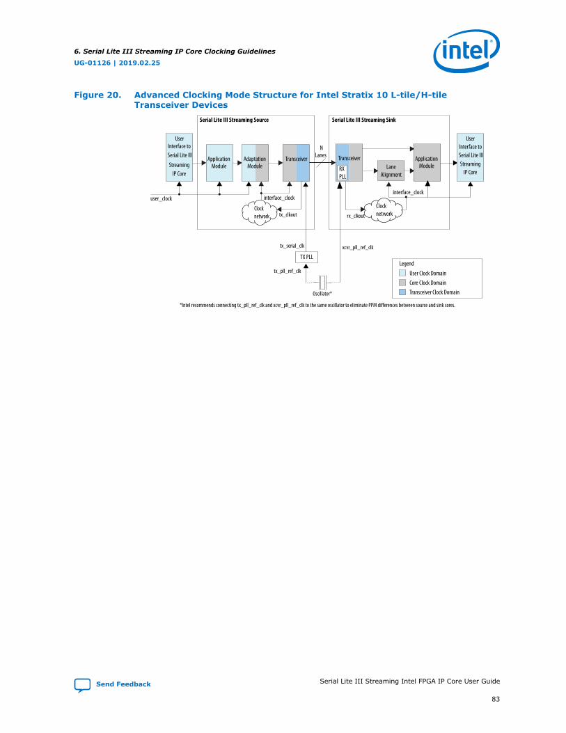
Figure 20. Advanced Clocking Mode Structure for Intel Stratix 10 L-tile/H-tileTransceiver Devices
ApplicationModule
Transceiver
Serial Lite III Streaming Source
AdaptationModule
user_clock
ApplicationModule
Transceiver
Serial Lite III Streaming Sink
LaneAlignment
NLanes
User Clock Domain
Legend
Core Clock DomainTransceiver Clock Domain
TX PLL
UserInterface toSerial Lite III
StreamingIP Core
UserInterface toSerial Lite IIIStreaming
IP Core
tx_serial_clk
tx_pll_ref_clk
xcvr_pll_ref_clk
tx_clkout rx_clkout
interface_clockinterface_clock
Clock network
Clock network
Oscillator*
*Intel recommends connecting tx_pll_ref_clk and xcvr_pll_ref_clk to the same oscillator to eliminate PPM differences between source and sink cores.
RXPLL
6. Serial Lite III Streaming IP Core Clocking Guidelines
UG-01126 | 2019.02.25
Send Feedback Serial Lite III Streaming Intel FPGA IP Core User Guide
83

Figure 21. Advanced Clocking Mode Structure for Intel Stratix 10 E-tile TransceiverDevices
ApplicationModule
Serial Lite III Streaming Duplex
AdaptationModule
user_clock
Application
Module
TX/RXTransceiver
LaneAlignment
NLanes
User Clock Domain
Legend
Core Clock DomainTransceiver Clock Domain
Clock network
UserInterface toSerial Lite IIIStreaming
IP Core
UserInterface toSerial Lite IIIStreaming
IP Core
tx_clkout
xcvr_pll_ref_clk
rx_clkout
user_clock
interface_clock
interface_clockClock network
NLanes
Table 36. Intel Stratix 10 Clocks in Advanced Clocking Mode
Clock Name Description
Source
user_clock User-defined. This clock is determined by the required throughput of the userapplication. For example, if the user interface is 384-bits wide (6 lanes × 64 bit/lane) and the required throughput is 120 Gbps, the user_clock frequency is312.5 MHz. This clock is an input to the IP core and you should toggle this at thespecified frequency.
tx_serial_clk This clock should toggle at one-half the data rate of the transceiver lane. Whenyou enter the user_clock frequency in the IP parameter editor, the per lanedata rate is calculated. Use that value and divided it by two to determine thetx_serial_clk. You are required to instantiate the TX PLL. In the Serial Lite IIIStreaming design example, an example of the TX PLL (ATX PLL) is generatedwith the IP core and is configured with the required reference clock andtx_serial_clk.Note: This signal is not available when you select E-Tile as as the transceiver
tile.
continued...
6. Serial Lite III Streaming IP Core Clocking Guidelines
UG-01126 | 2019.02.25
Serial Lite III Streaming Intel FPGA IP Core User Guide Send Feedback
84
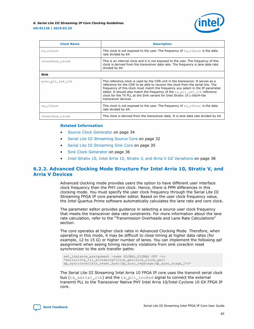
Clock Name Description
tx_clkout This clock is not exposed to the user. The frequency of tx_clkout is the datarate divided by 64.
interface_clock This is an internal clock and it is not exposed to the user. The frequency of thisclock is derived from the transceiver data rate. The frequency is lane data ratedivided by 64.
Sink
xcvr_pll_ref_clk This reference clock is used by the CDR unit in the transceiver. It serves as areference for the CDR to be able to recover the clock from the serial line. Thefrequency of this clock must match the frequency you select in the IP parametereditor. It should also match the frequency of the tx_pll_ref_clk referenceclock for the TX PLL at the Sink variant for Intel Stratix 10 L-tile/H-tiletransceiver devices.
rx_clkout This clock is not exposed to the user. The frequency of rx_clkout is the datarate divided by 64.
interface_clock This clock is derived from the transceiver data. It is lane data rate divided by 64.
Related Information
• Source Clock Generator on page 34
• Serial Lite III Streaming Source Core on page 32
• Serial Lite III Streaming Sink Core on page 35
• Sink Clock Generator on page 36
• Intel Stratix 10, Intel Arria 10, Stratix V, and Arria V GZ Variations on page 38
6.2.2. Advanced Clocking Mode Structure For Intel Arria 10, Stratix V, andArria V Devices
Advanced clocking mode provides users the option to have different user interfaceclock frequency than the PHY core clock. Hence, there is PPM differences in thisclocking mode. You must specify the user clock frequency through the Serial Lite IIIStreaming FPGA IP core parameter editor. Based on the user clock frequency value,the Intel Quartus Prime software automatically calculates the lane rate and core clock.
The parameter editor provides guidance in selecting a source user clock frequencythat meets the transceiver data rate constraints. For more information about the lanerate calculation, refer to the “Transmission Overheads and Lane Rate Calculations”section.
The core operates at higher clock rates in Advanced Clocking Mode. Therefore, whenoperating in this mode, it may be difficult to close timing at higher data rates (forexample, 12 to 15 G) or higher number of lanes. You can implement the following qsfassignment when seeing timing recovery violations from sink coreclkin resetsynchronizer to the sink transfer paths:
set_instance_assignment -name GLOBAL_SIGNAL OFF -to *seriallite_iii_streaming*clock_gen:sink_clock_gen|dp_sync:coreclkin_reset_sync|dp_sync_regstage:dp_sync_stage_2*o*
The Serial Lite III Streaming Intel Arria 10 FPGA IP core uses the transmit serial clockbus (tx_serial_clk) and the tx_pll_locked signal to connect the externaltransmit PLL to the Transceiver Native PHY Intel Arria 10/Intel Cyclone 10 GX FPGA IPcore.
6. Serial Lite III Streaming IP Core Clocking Guidelines
UG-01126 | 2019.02.25
Send Feedback Serial Lite III Streaming Intel FPGA IP Core User Guide
85

Note: For sink core, the IP core does not provide any adaptation module. Users shouldconsider a design that can manage the PPM differences between interface_clockand user interface clock.
Figure 22. Advanced Clocking Mode Structure for Intel Arria 10 Devices
ApplicationModule
Transceiver
Serial Lite III Streaming Source
AdaptationModule
user_clock interface_clock
ApplicationModule
Transceiver
Serial Lite III Streaming Sink
interface_clock
LaneAlignment
NLanes
User Clock Domain
Legend
Core Clock DomainTransceiver Clock Domain
TX PLL
User
Serial Lite IIIStreaming
IP Core
UserInterface to
Serial Lite IIIStreaming
IP Core
tx_serial_clk
tx_pll_ref_clk
xcvr_pll_ref_clk
Interface to
Oscillator*
*Intel recommends connecting tx_pll_ref_clk and xcvr_pll_ref_clk to the same oscillator to eliminate PPM differences between source and sink cores.
RXPLL
Figure 23. Advanced Clocking Mode Structure for Stratix V or Arria V Devices
ApplicationModule
Transceiver
Intel FPGA Serial Lite III Streaming Source
AdaptationModule
user_clock interface_clock
ApplicationModule
Transceiver
Intel FPGA Serial Lite III Streaming Sink
interface_clock
LaneAlignment
NLanes
User Clock Domain
Legend
Core Clock DomainTransceiver Clock Domain
TXPLL
UserInterface toSerial Lite IIIStreaming
IP Core
UserInterface toSerial Lite III
StreamingIP Core
tx_pll_ref_clk xcvr_pll_ref_clk
Oscillator*
*Intel recommends connecting tx_pll_ref_clk and xcvr_pll_ref_clk to the same oscillator to eliminate PPM differences between source and sink cores.
RXPLL
Table 37. Intel Arria 10, Stratix V, and Arria V Clocks in Advanced Clocking Mode
Clock Name Description
Source
user_clock User-defined. This clock is determined by the required throughput of the userapplication. For example, if the user interface is 384-bits wide (6 lanes × 64 bit/lane) and the required throughput is 120 Gbps, the user_clock frequency is312.5 MHz. This clock is an input to the IP core and you should toggle this at thespecified frequency.
tx_serial_clk (Intel Arria 10devices)
This clock should toggle at one-half the data rate of the transceiver lane. Whenyou enter the user_clock frequency in the IP parameter editor, the per lanedata rate is calculated. Use that value and divided it by two to determine the
continued...
6. Serial Lite III Streaming IP Core Clocking Guidelines
UG-01126 | 2019.02.25
Serial Lite III Streaming Intel FPGA IP Core User Guide Send Feedback
86

Clock Name Description
tx_serial_clk. You are required to instantiate the TX PLL. An example of theTX PLL (ATX PLL) is generated with the IP core and is configured with therequired reference clock and tx_serial_clk frequencies.
interface_clock (Stratix V andArria V devices)
This is an internal clock and it is not exposed to the user. The frequency of thisclock is derived from the transceiver data rate. It is lane data rate divided by 40.
interface_clock This is an internal clock and it is not exposed to the user. The frequency of thisclock is derived from the transceiver data rate. The frequency is lane data ratedivided by 64.
Sink
xcvr_pll_ref_clk This reference clock is used by the CDR unit in the transceiver. It serves as areference for the CDR to be able to recover the clock from the serial line. Thefrequency of this clock must match the frequency you select in the IP parametereditor. It should also match the frequency of the tx_pll_ref_clk referenceclock for the TX PLL at the Source variant.
interface_clock This clock is derived from the transceiver data. It is lane data rate divided by 64.It is an output of the IP core and should be used to clock the RX user application,
Example of Implementing Specific User Interface Clock Frequency
An application requires the Serial Lite III Streaming IP core to sustain a frequency of240 Gbps at the user interface.
user_clock (frequency) × number_of_lanes × 64 bits/lane = 240 Gbps
The data rate for Intel Arria 10 GX transceivers is limited to 17.4 Gbps. Therefore, 240Gbps / 17.4 Gbps = 14 (rounding up)
Choosing 14 lanes gives:
user_clock (frequency) = 240 / (14 × 64) = 267.86 MHz
A value of 267.86 MHz is out of the supported range for the user_clock frequency.Therefore, you need to add one more lane.
user_clock (frequency) = 240 / (15 × 64) = 250 MHz
Choosing 250 MHz as the user_clock, the IP core provides the following values:
Transceiver data rate: 16.78 Gbps
interface_clk: 16.78 / 64 = 262.18 MHz
tx_serial_clock: 16.78 Gbps / 2 = 8390 MHz
Related Information
• Source Clock Generator on page 34
• Serial Lite III Streaming Source Core on page 32
• Serial Lite III Streaming Sink Core on page 35
• Sink Clock Generator on page 36
• Intel Stratix 10, Intel Arria 10, Stratix V, and Arria V GZ Variations on page 38
6. Serial Lite III Streaming IP Core Clocking Guidelines
UG-01126 | 2019.02.25
Send Feedback Serial Lite III Streaming Intel FPGA IP Core User Guide
87

6.3. Standard Clocking Mode vs Advanced Clocking Mode
Table below lists the comparison between two clocking modes that the Serial Lite IIIStreaming Intel FPGA IP core supports.
Table 38. Clocking Mode Comparisons
Attribute Standard Clocking Mode Advanced Clocking Mode
Intel Stratix 10 Intel Arria 10,Stratix V, and Arria V
GZ
Intel Stratix 10 Intel Arria 10,Stratix V, and Arria V
GZ
User clock sourcing Generated by theuser, provided as aninput to the Serial LiteIII Streaming IntelFPGA IP core.
The user interfaceclock is generated bythe Serial Lite IIIStreaming Intel FPGAIP core, provided asan output to the user.
For source core. theuser interface clock isgenerated by the user.For sink core, Theinterface clock isgenerated by theSerial Lite IIIStreaming Intel FPGAIP core, provided asan output to the user.This mode issupported to providebackwardcompatibility whenmigrating the IP corefrom previous devices.
Generated by theuser, provided as aninput to the Serial LiteIII Streaming IntelFPGA IP core.
PPM differencesbetween userinterface clock andPHY core clock
YesIntel recommends touse the same clocksource as thetx_pll_ref_clk forzero clock PPMimplementation.
No Yes Yes
fPLL usageNote: The fPLLs are
located in theFPGA corefabric
Not used in eithersimplex or duplexcores.
Simplex: 1 per Sourcecore and 1 per Sinkcore per Serial Lite IIIStreaming Intel FPGAIP core instance.Duplex: 2 per SerialLite III StreamingIntel FPGA IP coreinstance.(Lane number doesnot factor in the useof fPLLs. Only theSerial Lite IIIStreaming Intel FPGAIP core instances arefactored in.)
Not used in eithersimplex or duplexcores.
Not used in eithersimplex or duplexcores.
Transmission overhead 1.1 1.1 Interlaken overheads Interlaken overheads
Related Information
Transmission Overheads and Lane Rate Calculations on page 39
6. Serial Lite III Streaming IP Core Clocking Guidelines
UG-01126 | 2019.02.25
Serial Lite III Streaming Intel FPGA IP Core User Guide Send Feedback
88

6.4. Clocking Implementation Guidelines
Synchronous Systems
In this scenario, both the Source User Clock and Sink FIFO read clock frequencies arethe same. As shown in the figure below, the FIFO read clock is derived from the samecrystal oscillator as the Source User Clock. If the Source User Clock requires a PLL, theSink User Clock should has a PLL with the same configuration.
Figure 24. Same Source and Sink User Clock Frequencies from Same Crystal Oscillatorfor Intel Stratix 10 L-tile/H-tile Transceiver Devices
ApplicationModule
Transceiver
Intel FPGA Serial Lite III Streaming Source
AdaptationModule
user_clock interface_clock
ApplicationModule
Transceiver
Intel FPGA Serial Lite III Streaming Sink
interface_clock
LaneAlignment
NLanes
TX PLL
UserInterface to
Serial Lite IIIStreaming
IP Core
User SinkFIFO
tx_serial_clk xcvr_pll_ref_clk
User Clock Domain
Legend
Core Clock DomainTransceiver Clock Domain
Global clock
network
Global clock
network
user_clock
Intel FPGA
Figure 25. Same Source and Sink User Clock Frequencies from Same Crystal Oscillatorfor Intel Arria 10, Stratix V and Arria V GZ Devices
ApplicationModule
Transceiver
Intel FPGA Serial Lite III Streaming Source
AdaptationModule
user_clock interface_clock
ApplicationModule
Transceiver
Intel FPGA Serial Lite III Streaming Sink
interface_clock
LaneAlignment
NLanes
TX PLL
UserInterface to
Serial Lite IIIStreaming
IP Core
User SinkFIFO
tx_serial_clk xcvr_pll_ref_clk
User Clock Domain
Legend
Core Clock DomainTransceiver Clock Domain
Intel FPGA
6. Serial Lite III Streaming IP Core Clocking Guidelines
UG-01126 | 2019.02.25
Send Feedback Serial Lite III Streaming Intel FPGA IP Core User Guide
89

Asynchronous Systems
In an asynchronous system, the sink FIFO read clock is derived from a differentcrystal oscillator, but has the same frequency as the Source User Clock. In thisscenario, a PPM difference exists between the Source User Clock and the FIFO readclock. The Source input data rate needs to be reduced to avoid overflowing the SinkFIFO buffer due to the PPM differences. One recommended way is to insert emptycycles in the Source input data stream at Source User Data Interface to reduce thedata rate. The Source Application and Adaptation modules absorb these empty datacycles, convert them to idle cells, and insert them into link data stream. These cellsare automatically removed at the sink interface and converted back into empty cycleson the sink user interface.
Note: You have to take into consideration the PPM difference and insert enough empty cyclesto offset the PPM difference for the worst case scenario.
Figure 26. Same Source and Sink User Frequencies with Different Crystal Oscillators forIntel Stratix 10 L-tile/H-tile Transceiver Devices
ApplicationModule
Transceiver
Intel FPGA Serial Lite III Streaming Source
AdaptationModule
user_clock interface_clock
ApplicationModule
Transceiver
Intel FPGA Serial Lite III Streaming Sink
interface_clock
LaneAlignment
NLanes
TX PLL
UserInterface to
Serial Lite IIIStreaming
IP Core
User SinkFIFO
tx_serial_clk xcvr_pll_ref_clk
User Clock Domain
Legend
Core Clock DomainTransceiver Clock Domain
Global clock
networkuser_clock
Global clock
network
Intel FPGA
6. Serial Lite III Streaming IP Core Clocking Guidelines
UG-01126 | 2019.02.25
Serial Lite III Streaming Intel FPGA IP Core User Guide Send Feedback
90
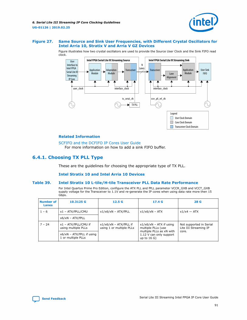
Figure 27. Same Source and Sink User Frequencies, with Different Crystal Oscillators forIntel Arria 10, Stratix V and Arria V GZ DevicesFigure illustrates how two crystal oscillators are used to provide the Source User Clock and the Sink FIFO readclock.
ApplicationModule
Transceiver
Intel FPGA Serial Lite III Streaming Source
AdaptationModule
user_clock interface_clock
ApplicationModule
Transceiver
Intel FPGA Serial Lite III Streaming Sink
interface_clock
LaneAlignment
NLanes
TX PLL
UserInterface to
Serial Lite IIIStreaming
IP Core
User SinkFIFO
tx_serial_clk xcvr_pll_ref_clk
User Clock Domain
Legend
Core Clock DomainTransceiver Clock Domain
Intel FPGA
Related Information
SCFIFO and the DCFIFO IP Cores User GuideFor more information on how to add a sink FIFO buffer.
6.4.1. Choosing TX PLL Type
These are the guidelines for choosing the appropriate type of TX PLL.
Intel Stratix 10 and Intel Arria 10 Devices
Table 39. Intel Stratix 10 L-tile/H-tile Transceiver PLL Data Rate PerformanceFor Intel Quartus Prime Pro Edition, configure the ATX PLL and fPLL parameter VCCR_GXB and VCCT_GXBsupply voltage for the Transceiver to 1.1V and re-generate the IP cores when using data rate more then 15Gbps.
Number ofLanes
10.3125 G 12.5 G 17.4 G 28 G
1 – 6 x1 – ATX/fPLL/CMU x1/x6/xN – ATX/fPLL x1/x6/xN – ATX x1/x4 — ATX
x6/xN – ATX/fPLL
7 – 24 x1 – ATX/fPLL/CMU ifusing multiple PLLs
x1/x6/xN – ATX/fPLL ifusing 1 or multiple PLLs
x1/x6/xN – ATX if usingmultiple PLLs (usemultiple PLLs as xN with1.12 V can only supportup to 16 G)
Not supported in SerialLite III Streaming IPcore.
x6/xN – ATX/fPLL if using1 or multiple PLLs
6. Serial Lite III Streaming IP Core Clocking Guidelines
UG-01126 | 2019.02.25
Send Feedback Serial Lite III Streaming Intel FPGA IP Core User Guide
91

Table 40. Intel Arria 10 PLL Data Rate Performance
Number ofLanes
10.3125 G 12.5 G 17.4 G
1 – 6 x1 – ATX/fPLL/CMU x1/x6/xN – ATX/fPLL x1/x6/xN – ATX
x6/xN – ATX/fPLL
7 – 24 x1 – ATX/fPLL/CMU if usingmultiple PLLs
x1/x6/xN – ATX/fPLL if using 1 ormultiple PLLs
x1/x6/xN – ATX if using multiplePLLs (use multiple PLLs as xNwith 1.12 V can only support upto 16 G)x6/xN – ATX/fPLL if using 1 or
multiple PLLs
For ATX PLL VCO frequencies between 7.2 GHz and 11.4 GHz, when two ATX PLLsoperate at the same VCO frequency (within 100 MHz), place the ATX PLLs with the gapof seven ATX PLLs apart (skip 6). For ATX PLL VCO frequencies between 11.4 GHz and14.4 GHz, when two ATX PLLs operate at the same VCO frequency (within 100 MHz),place the ATX PLLs with the gap of four ATX PLLs apart (skip 3). If these spacing rulesare violated, the Intel Quartus Prime issues a critical warning. The maximum channelspan of a xN clock network is two transceiver banks above and two transceiver banksbelow the bank that contains the driving PLL and the master CGB. You can use amaximum of 30 channels in a single-bonded or non-bonded xN group. The maximumdata rate supported by the xN clock network while driving channels in either thebonded or non-bonded mode depends on the voltage used to drive the transceiverbanks and the transceiver speed grade.
Stratix V and Arria V Devices
The Serial Lite III Streaming Intel FPGA IP core in Stratix V and Arria V devices allow aselection of PLL type for use inside the transmit and receive PMA blocks. The IPparameter editor in Intel Quartus Prime Standard Edition allows you to select either aCMU PLL or an ATX PLL. The CMU PLL is more suitable for lower lane data rates, whilethe ATX PLL is better for higher lane data rates. The supported data rates for the CMUPLL and ATX PLL are provided in Tables 1 (Stratix V) and 2 (Arria V GZ). These tableslist the maximum lane data rates per transceiver speed grade. For example, if yourdesign requires a 14.1 Gbps lane rate, you need to use an ATX PLL and select aTransceiver Speed Grade 1 device.
Table 41. Stratix V CMU and ATX PLL Supported Data RatesFor more information about the Stratix V devices, refer to the device datasheet.
Symbol/Description
Conditions Transceiver Speed Grade1 (Mbps)
Transceiver Speed Grade2 (Mbps)
Transceiver Speed Grade3 (Mbps)
Min Typ Max Min Typ Max Min Typ Max
CMU PLLSupported DataRange
_ 600 _ 12500 600 _ 12500 600 _ 8500
ATX PLLSupported DataRange
VCOPost-dividerL=2
8000 _ 14100 8000 _ 12500 8000 _ 8500
L=4 4000 _ 7050 4000 _ 6600 4000 6600
L=8 2000 _ 3525 2000 _ 3300 2000 _ 3300
6. Serial Lite III Streaming IP Core Clocking Guidelines
UG-01126 | 2019.02.25
Serial Lite III Streaming Intel FPGA IP Core User Guide Send Feedback
92
Table 42. Arria V GZ CMU and ATX PLL Supported Data RatesFor more information about the Arria V GZ devices, refer to the device datasheet.
Symbol/ Description Conditions Transceiver Speed Grade 2(Mbps)
Transceiver Speed Grade 3(Mbps)
Min Typ Max Min Typ Max
CMU PLL Supported DataRange
_ 600 _ 12500 600 _ 10312.5
ATX PLL Supported DataRange
VCOPost-divider L=2
8000 _ 12500 8000 _ 10312.5
L=4 4000 _ 6600 4000 6600
L=8 2000 _ 3300 2000 _ 3300
Related Information
• Intel Stratix 10 L- and H-Tile Transceiver PHY User Guide - DynamicReconfiguration Parameters
• Intel Stratix 10 E-Tile Transceiver PHY User GuideFor more information about the Intel Stratix 10 E-Tile Native PHY IP core.
• V-Series Transceiver PHY User Guide
• Stratix V Device Datasheet
• Arria V GZ Device Datasheet
• Intel Arria 10 Device Datasheet Guide
• Intel Stratix 10 Device Datasheet Guide
• Intel Arria 10 Transceiver PHY User GuideFor more information about the PLL types in Intel Arria 10 Transceiver PHY
• Intel Stratix 10 E-Tile Transceiver PHY User GuideFor more information about the Intel Stratix 10 E-Tile Native PHY IP core.
6.5. Core Latency
The table below lists the latency measurement for the Serial Lite III Streaming IP coreduplex core in standard and advanced clocking mode. An average value is taken froma set of samples during hardware testing.
For a loopback scenario, the core latency measurement is based on the round triplatency from the TX core input to RX core output.
Table 43. Latency Measurement for Duplex Core
Device Clocking Mode Parameters Latency (ns)
Number of Lanes Per-Lane Data Rate(Mbps)
Intel Stratix 10 E-tileTransceiver
Standard 6 12,500 574.464
Advanced 6 12,500 533.573
Intel Stratix 10 L-tile/H-tile Transceiver
Standard 6 12,500 304.128
Advanced 6 12,500 272.810
continued...
6. Serial Lite III Streaming IP Core Clocking Guidelines
UG-01126 | 2019.02.25
Send Feedback Serial Lite III Streaming Intel FPGA IP Core User Guide
93
Device Clocking Mode Parameters Latency (ns)
Number of Lanes Per-Lane Data Rate(Mbps)
Intel Arria 10 Standard 5 17,400 174.064
Advanced 5 17,400 154.996
Stratix V, Arria V GZ Standard 5 10,312.50 320.964
Advanced 5 10,312.50 292.712
Note: To calculate the latency for 17,400 Mbps per lane data rate, an average value wastaken from a set of samples. For duplex advanced clocking mode, the latencies variedmore in simulation.
6. Serial Lite III Streaming IP Core Clocking Guidelines
UG-01126 | 2019.02.25
Serial Lite III Streaming Intel FPGA IP Core User Guide Send Feedback
94
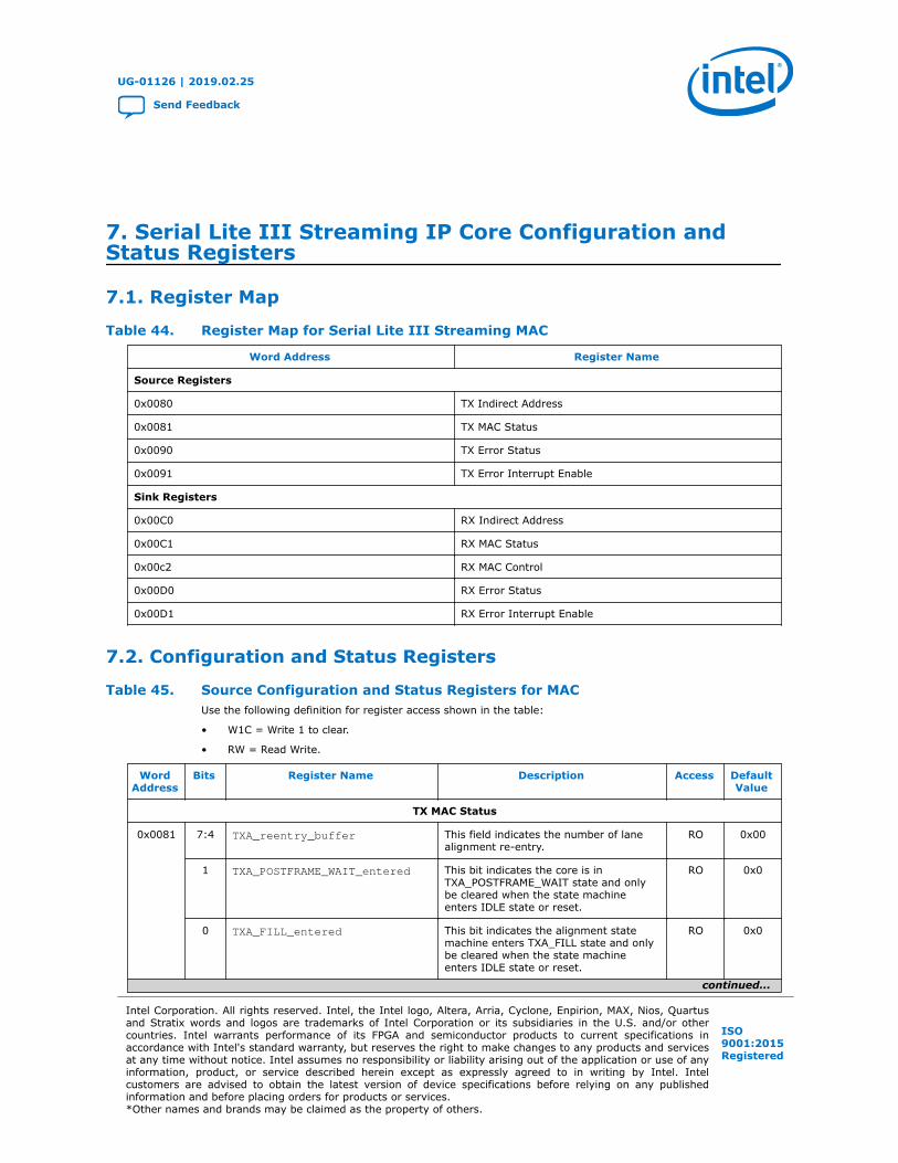
7. Serial Lite III Streaming IP Core Configuration andStatus Registers
7.1. Register Map
Table 44. Register Map for Serial Lite III Streaming MAC
Word Address Register Name
Source Registers
0x0080 TX Indirect Address
0x0081 TX MAC Status
0x0090 TX Error Status
0x0091 TX Error Interrupt Enable
Sink Registers
0x00C0 RX Indirect Address
0x00C1 RX MAC Status
0x00c2 RX MAC Control
0x00D0 RX Error Status
0x00D1 RX Error Interrupt Enable
7.2. Configuration and Status Registers
Table 45. Source Configuration and Status Registers for MACUse the following definition for register access shown in the table:
• W1C = Write 1 to clear.
• RW = Read Write.
WordAddress
Bits Register Name Description Access DefaultValue
TX MAC Status
0x0081 7:4 TXA_reentry_buffer This field indicates the number of lanealignment re-entry.
RO 0x00
1 TXA_POSTFRAME_WAIT_entered This bit indicates the core is inTXA_POSTFRAME_WAIT state and onlybe cleared when the state machineenters IDLE state or reset.
RO 0x0
0 TXA_FILL_entered This bit indicates the alignment statemachine enters TXA_FILL state and onlybe cleared when the state machineenters IDLE state or reset.
RO 0x0
continued...
UG-01126 | 2019.02.25
Send Feedback
Intel Corporation. All rights reserved. Intel, the Intel logo, Altera, Arria, Cyclone, Enpirion, MAX, Nios, Quartusand Stratix words and logos are trademarks of Intel Corporation or its subsidiaries in the U.S. and/or othercountries. Intel warrants performance of its FPGA and semiconductor products to current specifications inaccordance with Intel's standard warranty, but reserves the right to make changes to any products and servicesat any time without notice. Intel assumes no responsibility or liability arising out of the application or use of anyinformation, product, or service described herein except as expressly agreed to in writing by Intel. Intelcustomers are advised to obtain the latest version of device specifications before relying on any publishedinformation and before placing orders for products or services.*Other names and brands may be claimed as the property of others.
ISO9001:2015Registered

WordAddress
Bits Register Name Description Access DefaultValue
TX Error Status Register
0x0090 6 tx_burst_gap_err TX burst gap error.This bit is set when the gap between twoconsecutive bursts (or packets) on TXuser data interface is less than therequired BURST_GAP (a synthesisoption). When this error happens, makesure the user interface behavior andBURST_GAP are matching.
W1C 0x0
5 ecc_err_fatal TX ECC Error Fatal consolidated status(of all lanes).This bit is set when double bit error isdetected and uncorrected.
W1C 0x0
4 ecc_err_corrected TX ECC Error Corrected consolidatedstatus (of all lanes).This bit is set when single bit error isdetected and corrected.
W1C 0x0
3 adapt_fifo_overflow TX MAC Adaptation FIFO overflowconsolidated status (of all lanes).In normal condition with all clocksrunning correctly, this bit is set when theuser data rate is faster thanexpected.When this happens, stopfurther data transfer and check if theclocks are set correctly.
W1C 0x0
2 tx_sync_done_lost TX Lost of Lane Alignment consolidatedstatus (of all lanes).
W1C 0x0
1 phy_fifo_underflow TX PHY Phase Compensation FIFOunderflow consolidated status (of alllanes).This bit is set when the IP core has majorerror and requires a full IP core reset.
W1C 0x0
0 phy_fifo_overflow TX PHY Phase Compensation FIFOoverflow consolidated status (of alllanes).This bit is set when the IP core has majorerror and requires a full IP core reset.
W1C 0x0
TX Error Interrupt Enable Register
0x0091 6 tx_burst_gap_err_en Set this bit to 1 to enable the Burst GapError Interrupt.
RW 0x1
5 ecc_err_fatal_en Set this bit to 1 to enable the ECCUncorrected Error Interrupt.
RW 0x0
4 ecc_err_corrected_en Set this bit to 1 to enable the ECCCorrected Error Interrupt.
RW 0x0
3 adapt_fifo_overflow_en Set this bit to 1 to enable the AdaptationFIFO Overflow Interrupt.
RW 0x1
2 tx_sync_donelost_en Set this bit to 1 to enable the Loss ofLane Alignment Interrupt.
RW 0x0
1 phy_fifo_underflow_en Set this bit to 1 to enable the PHY FIFOEmpty Interrupt.
RW 0x0
0 phy_fifo_overflow_en Set this bit to 1 to enable the PHY FIFOError Interrupt.
RW 0x0
7. Serial Lite III Streaming IP Core Configuration and Status Registers
UG-01126 | 2019.02.25
Serial Lite III Streaming Intel FPGA IP Core User Guide Send Feedback
96
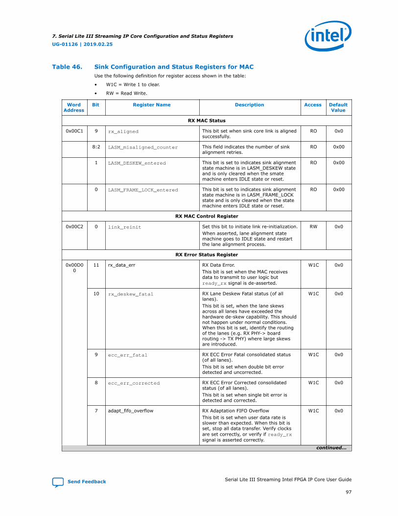
Table 46. Sink Configuration and Status Registers for MACUse the following definition for register access shown in the table:
• W1C = Write 1 to clear.
• RW = Read Write.
WordAddress
Bit Register Name Description Access DefaultValue
RX MAC Status
0x00C1 9 rx_aligned This bit set when sink core link is alignedsuccessfully.
RO 0x0
8:2 LASM_misaligned_counter This field indicates the number of sinkalignment retries.
RO 0x00
1 LASM_DESKEW_entered This bit is set to indicates sink alignmentstate machine is in LASM_DESKEW stateand is only cleared when the smatemachine enters IDLE state or reset.
RO 0x00
0 LASM_FRAME_LOCK_entered This bit is set to indicates sink alignmentstate machine is in LASM_FRAME_LOCKstate and is only cleared when the statemachine enters IDLE state or reset.
RO 0x00
RX MAC Control Register
0x00C2 0 link_reinit Set this bit to initiate link re-initialization.When asserted, lane alignment statemachine goes to IDLE state and restartthe lane alignment process.
RW 0x0
RX Error Status Register
0x00D00
11 rx_data_err RX Data Error.This bit is set when the MAC receivesdata to transmit to user logic butready_rx signal is de-asserted.
W1C 0x0
10 rx_deskew_fatal RX Lane Deskew Fatal status (of alllanes).This bit is set, when the lane skewsacross all lanes have exceeded thehardware de-skew capability. This shouldnot happen under normal conditions.When this bit is set, identify the routingof the lanes (e.g. RX PHY-> boardrouting -> TX PHY) where large skewsare introduced.
W1C 0x0
9 ecc_err_fatal RX ECC Error Fatal consolidated status(of all lanes).This bit is set when double bit errordetected and uncorrected.
W1C 0x0
8 ecc_err_corrected RX ECC Error Corrected consolidatedstatus (of all lanes).This bit is set when single bit error isdetected and corrected.
W1C 0x0
7 adapt_fifo_overflow RX Adaptation FIFO OverflowThis bit is set when user data rate isslower than expected. When this bit isset, stop all data transfer. Verify clocksare set correctly, or verify if ready_rxsignal is asserted correctly.
W1C 0x0
continued...
7. Serial Lite III Streaming IP Core Configuration and Status Registers
UG-01126 | 2019.02.25
Send Feedback Serial Lite III Streaming Intel FPGA IP Core User Guide
97
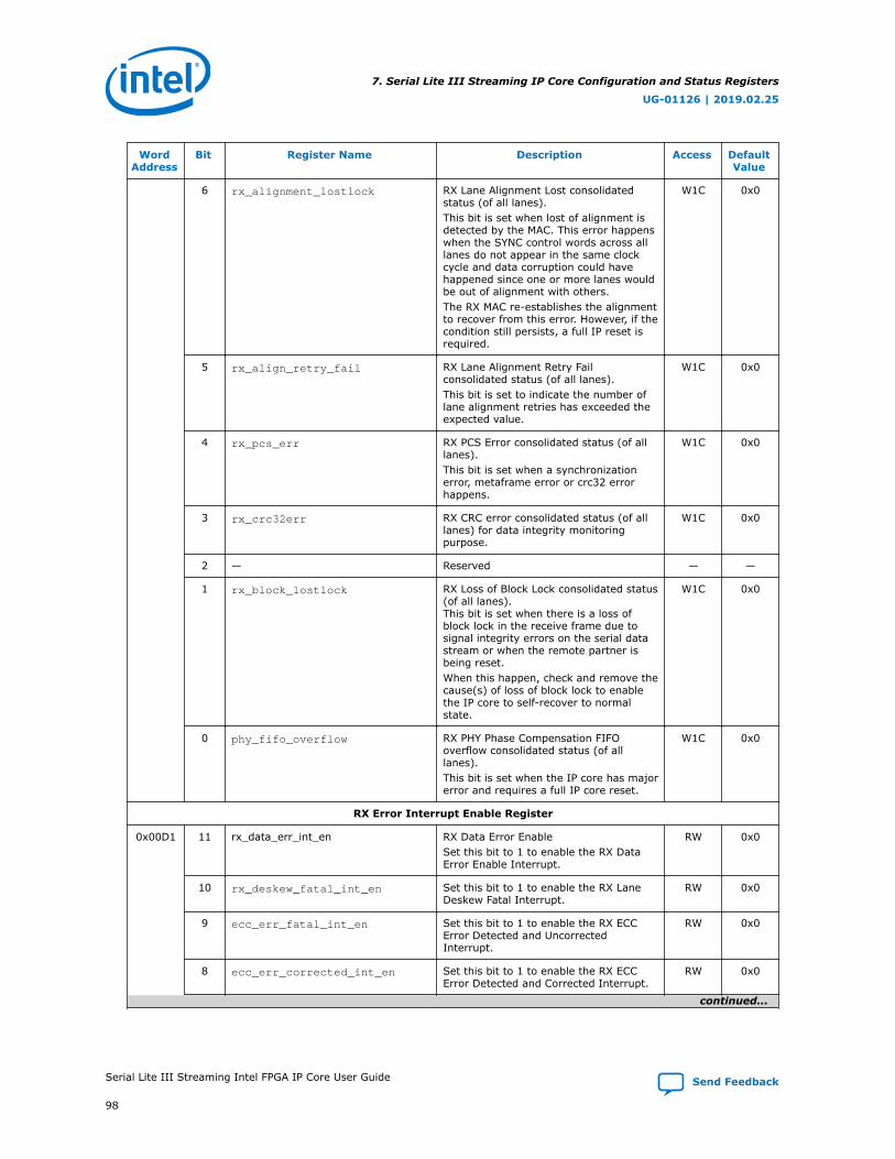
WordAddress
Bit Register Name Description Access DefaultValue
6 rx_alignment_lostlock RX Lane Alignment Lost consolidatedstatus (of all lanes).This bit is set when lost of alignment isdetected by the MAC. This error happenswhen the SYNC control words across alllanes do not appear in the same clockcycle and data corruption could havehappened since one or more lanes wouldbe out of alignment with others.The RX MAC re-establishes the alignmentto recover from this error. However, if thecondition still persists, a full IP reset isrequired.
W1C 0x0
5 rx_align_retry_fail RX Lane Alignment Retry Failconsolidated status (of all lanes).This bit is set to indicate the number oflane alignment retries has exceeded theexpected value.
W1C 0x0
4 rx_pcs_err RX PCS Error consolidated status (of alllanes).This bit is set when a synchronizationerror, metaframe error or crc32 errorhappens.
W1C 0x0
3 rx_crc32err RX CRC error consolidated status (of alllanes) for data integrity monitoringpurpose.
W1C 0x0
2 — Reserved — —
1 rx_block_lostlock RX Loss of Block Lock consolidated status(of all lanes).This bit is set when there is a loss ofblock lock in the receive frame due tosignal integrity errors on the serial datastream or when the remote partner isbeing reset.When this happen, check and remove thecause(s) of loss of block lock to enablethe IP core to self-recover to normalstate.
W1C 0x0
0 phy_fifo_overflow RX PHY Phase Compensation FIFOoverflow consolidated status (of alllanes).This bit is set when the IP core has majorerror and requires a full IP core reset.
W1C 0x0
RX Error Interrupt Enable Register
0x00D1 11 rx_data_err_int_en RX Data Error EnableSet this bit to 1 to enable the RX DataError Enable Interrupt.
RW 0x0
10 rx_deskew_fatal_int_en Set this bit to 1 to enable the RX LaneDeskew Fatal Interrupt.
RW 0x0
9 ecc_err_fatal_int_en Set this bit to 1 to enable the RX ECCError Detected and UncorrectedInterrupt.
RW 0x0
8 ecc_err_corrected_int_en Set this bit to 1 to enable the RX ECCError Detected and Corrected Interrupt.
RW 0x0
continued...
7. Serial Lite III Streaming IP Core Configuration and Status Registers
UG-01126 | 2019.02.25
Serial Lite III Streaming Intel FPGA IP Core User Guide Send Feedback
98
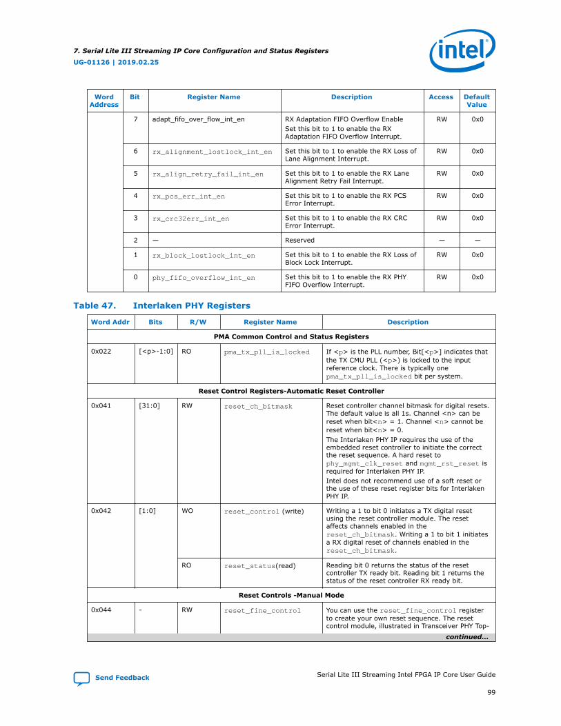
WordAddress
Bit Register Name Description Access DefaultValue
7 adapt_fifo_over_flow_int_en RX Adaptation FIFO Overflow EnableSet this bit to 1 to enable the RXAdaptation FIFO Overflow Interrupt.
RW 0x0
6 rx_alignment_lostlock_int_en Set this bit to 1 to enable the RX Loss ofLane Alignment Interrupt.
RW 0x0
5 rx_align_retry_fail_int_en Set this bit to 1 to enable the RX LaneAlignment Retry Fail Interrupt.
RW 0x0
4 rx_pcs_err_int_en Set this bit to 1 to enable the RX PCSError Interrupt.
RW 0x0
3 rx_crc32err_int_en Set this bit to 1 to enable the RX CRCError Interrupt.
RW 0x0
2 — Reserved — —
1 rx_block_lostlock_int_en Set this bit to 1 to enable the RX Loss ofBlock Lock Interrupt.
RW 0x0
0 phy_fifo_overflow_int_en Set this bit to 1 to enable the RX PHYFIFO Overflow Interrupt.
RW 0x0
Table 47. Interlaken PHY Registers
Word Addr Bits R/W Register Name Description
PMA Common Control and Status Registers
0x022 [<p>-1:0] RO pma_tx_pll_is_locked If <p> is the PLL number, Bit[<p>] indicates thatthe TX CMU PLL (<p>) is locked to the inputreference clock. There is typically onepma_tx_pll_is_locked bit per system.
Reset Control Registers-Automatic Reset Controller
0x041 [31:0] RW reset_ch_bitmask Reset controller channel bitmask for digital resets.The default value is all 1s. Channel <n> can bereset when bit<n> = 1. Channel <n> cannot bereset when bit<n> = 0.The Interlaken PHY IP requires the use of theembedded reset controller to initiate the correctthe reset sequence. A hard reset tophy_mgmt_clk_reset and mgmt_rst_reset isrequired for Interlaken PHY IP.Intel does not recommend use of a soft reset orthe use of these reset register bits for InterlakenPHY IP.
0x042 [1:0] WO reset_control (write) Writing a 1 to bit 0 initiates a TX digital resetusing the reset controller module. The resetaffects channels enabled in thereset_ch_bitmask. Writing a 1 to bit 1 initiatesa RX digital reset of channels enabled in thereset_ch_bitmask.
RO reset_status(read) Reading bit 0 returns the status of the resetcontroller TX ready bit. Reading bit 1 returns thestatus of the reset controller RX ready bit.
Reset Controls -Manual Mode
0x044 - RW reset_fine_control You can use the reset_fine_control registerto create your own reset sequence. The resetcontrol module, illustrated in Transceiver PHY Top-
continued...
7. Serial Lite III Streaming IP Core Configuration and Status Registers
UG-01126 | 2019.02.25
Send Feedback Serial Lite III Streaming Intel FPGA IP Core User Guide
99
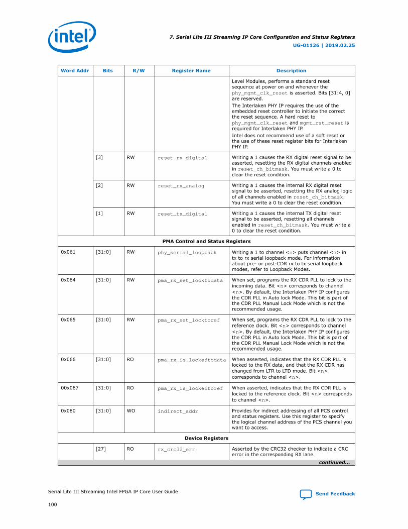
Word Addr Bits R/W Register Name Description
Level Modules, performs a standard resetsequence at power on and whenever thephy_mgmt_clk_reset is asserted. Bits [31:4, 0]are reserved.The Interlaken PHY IP requires the use of theembedded reset controller to initiate the correctthe reset sequence. A hard reset tophy_mgmt_clk_reset and mgmt_rst_reset isrequired for Interlaken PHY IP.Intel does not recommend use of a soft reset orthe use of these reset register bits for InterlakenPHY IP.
[3] RW reset_rx_digital Writing a 1 causes the RX digital reset signal to beasserted, resetting the RX digital channels enabledin reset_ch_bitmask. You must write a 0 toclear the reset condition.
[2] RW reset_rx_analog Writing a 1 causes the internal RX digital resetsignal to be asserted, resetting the RX analog logicof all channels enabled in reset_ch_bitmask.You must write a 0 to clear the reset condition.
[1] RW reset_tx_digital Writing a 1 causes the internal TX digital resetsignal to be asserted, resetting all channelsenabled in reset_ch_bitmask. You must write a0 to clear the reset condition.
PMA Control and Status Registers
0x061 [31:0] RW phy_serial_loopback Writing a 1 to channel <n> puts channel <n> intx to rx serial loopback mode. For informationabout pre- or post-CDR rx to tx serial loopbackmodes, refer to Loopback Modes.
0x064 [31:0] RW pma_rx_set_locktodata When set, programs the RX CDR PLL to lock to theincoming data. Bit <n> corresponds to channel<n>. By default, the Interlaken PHY IP configuresthe CDR PLL in Auto lock Mode. This bit is part ofthe CDR PLL Manual Lock Mode which is not therecommended usage.
0x065 [31:0] RW pma_rx_set_locktoref When set, programs the RX CDR PLL to lock to thereference clock. Bit <n> corresponds to channel<n>. By default, the Interlaken PHY IP configuresthe CDR PLL in Auto lock Mode. This bit is part ofthe CDR PLL Manual Lock Mode which is not therecommended usage.
0x066 [31:0] RO pma_rx_is_lockedtodata When asserted, indicates that the RX CDR PLL islocked to the RX data, and that the RX CDR haschanged from LTR to LTD mode. Bit <n>corresponds to channel <n>.
00x067 [31:0] RO pma_rx_is_lockedtoref When asserted, indicates that the RX CDR PLL islocked to the reference clock. Bit <n> correspondsto channel <n>.
0x080 [31:0] WO indirect_addr Provides for indirect addressing of all PCS controland status registers. Use this register to specifythe logical channel address of the PCS channel youwant to access.
Device Registers
[27] RO rx_crc32_err Asserted by the CRC32 checker to indicate a CRCerror in the corresponding RX lane.
continued...
7. Serial Lite III Streaming IP Core Configuration and Status Registers
UG-01126 | 2019.02.25
Serial Lite III Streaming Intel FPGA IP Core User Guide Send Feedback
100
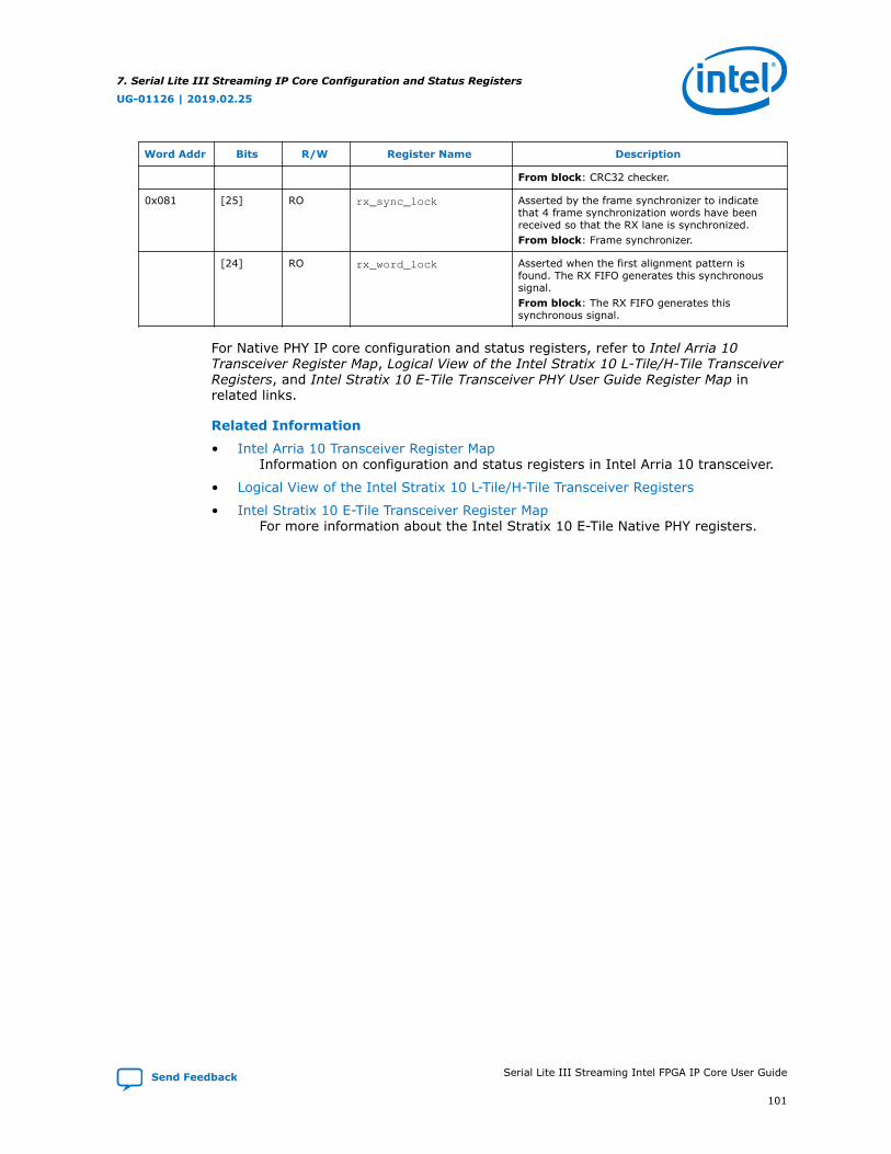
Word Addr Bits R/W Register Name Description
From block: CRC32 checker.
0x081 [25] RO rx_sync_lock Asserted by the frame synchronizer to indicatethat 4 frame synchronization words have beenreceived so that the RX lane is synchronized.From block: Frame synchronizer.
[24] RO rx_word_lock Asserted when the first alignment pattern isfound. The RX FIFO generates this synchronoussignal.From block: The RX FIFO generates thissynchronous signal.
For Native PHY IP core configuration and status registers, refer to Intel Arria 10Transceiver Register Map, Logical View of the Intel Stratix 10 L-Tile/H-Tile TransceiverRegisters, and Intel Stratix 10 E-Tile Transceiver PHY User Guide Register Map inrelated links.
Related Information
• Intel Arria 10 Transceiver Register MapInformation on configuration and status registers in Intel Arria 10 transceiver.
• Logical View of the Intel Stratix 10 L-Tile/H-Tile Transceiver Registers
• Intel Stratix 10 E-Tile Transceiver Register MapFor more information about the Intel Stratix 10 E-Tile Native PHY registers.
7. Serial Lite III Streaming IP Core Configuration and Status Registers
UG-01126 | 2019.02.25
Send Feedback Serial Lite III Streaming Intel FPGA IP Core User Guide
101
8. Serial Lite III Streaming IP Core Debugging GuidelinesThis section includes guidelines to assist you in debugging the IP core link issues.
8.1. Creating a Signal Tap Debug File to Match Your DesignHierarchy
For Intel Arria 10 and Intel Stratix 10 devices, the Intel Quartus Prime softwaregenerates two files, build_stp.tcl and <ip_core_name>.xml. You can use thesefiles to generate a Signal Tap file with probe points matching your design hierarchy.
The Intel Quartus Prime software stores these files in the <IP core directory>/synth/debug/stp/ directory.
Synthesize your design using the Intel Quartus Prime software.
1. To open the Tcl console, click View ➤ Utility Windows ➤ Tcl Console.
2. Type the following command in the Tcl console:source <IP core directory>/synth/debug/stp/build_stp.tcl
3. To generate the STP file, type the following command:main -stp_file <output stp file name>.stp -xml_file <inputxml_file name>.xml -mode build
4. To add this Signal Tap file (.stp) to your project, select Project ➤ Add/RemoveFiles in Project. Then, compile your design.
5. To program the FPGA, click Tools ➤ Programmer.
6. To start the Signal Tap Logic Analyzer, click Quartus Prime ➤ Tools ➤ SignalTap Logic Analyzer.
The software generation script may not assign the Signal Tap acquisition clock in<output stp file name>.stp. Consequently, the Intel Quartus Primesoftware automatically creates a clock pin called auto_stp_external_clock.You may need to manually substitute the appropriate clock signal as the SignalTap sampling clock for each STP instance.
7. Recompile your design.
8. To observe the state of your IP core, click Run Analysis.
You may see signals or Signal Tap instances that are red, indicating they are notavailable in your design. In most cases, you can safely ignore these signals andinstances. They are present because software generates wider buses and someinstances that your design does not include.
UG-01126 | 2019.02.25
Send Feedback
Intel Corporation. All rights reserved. Intel, the Intel logo, Altera, Arria, Cyclone, Enpirion, MAX, Nios, Quartusand Stratix words and logos are trademarks of Intel Corporation or its subsidiaries in the U.S. and/or othercountries. Intel warrants performance of its FPGA and semiconductor products to current specifications inaccordance with Intel's standard warranty, but reserves the right to make changes to any products and servicesat any time without notice. Intel assumes no responsibility or liability arising out of the application or use of anyinformation, product, or service described herein except as expressly agreed to in writing by Intel. Intelcustomers are advised to obtain the latest version of device specifications before relying on any publishedinformation and before placing orders for products or services.*Other names and brands may be claimed as the property of others.
ISO9001:2015Registered
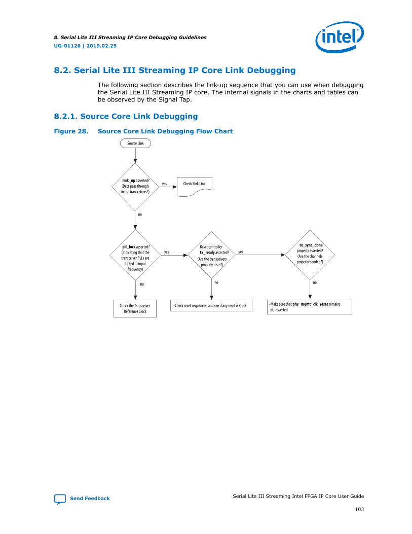
8.2. Serial Lite III Streaming IP Core Link Debugging
The following section describes the link-up sequence that you can use when debuggingthe Serial Lite III Streaming IP core. The internal signals in the charts and tables canbe observed by the Signal Tap.
8.2.1. Source Core Link Debugging
Figure 28. Source Core Link Debugging Flow Chart
Source Link
Iink_up asserted?(Data pass through
to the transceivers?)
yes
no
Reset controller tx_ready asserted?
(Are the transceiversproperly reset?)
yes
no
tx_sync_doneproperly asserted?(Are the channelsproperly bonded?)
no
pll_lock asserted?(Indicating that thetransceiver PLLs are
locked to inputfrequency)
yes
no
Check Sink Link
Check the TransceiverReference Clock
-Make sure that phy_mgmt_clk_reset remains de-asserted
-Check reset sequences, and see if any reset is stuck
8. Serial Lite III Streaming IP Core Debugging Guidelines
UG-01126 | 2019.02.25
Send Feedback Serial Lite III Streaming Intel FPGA IP Core User Guide
103
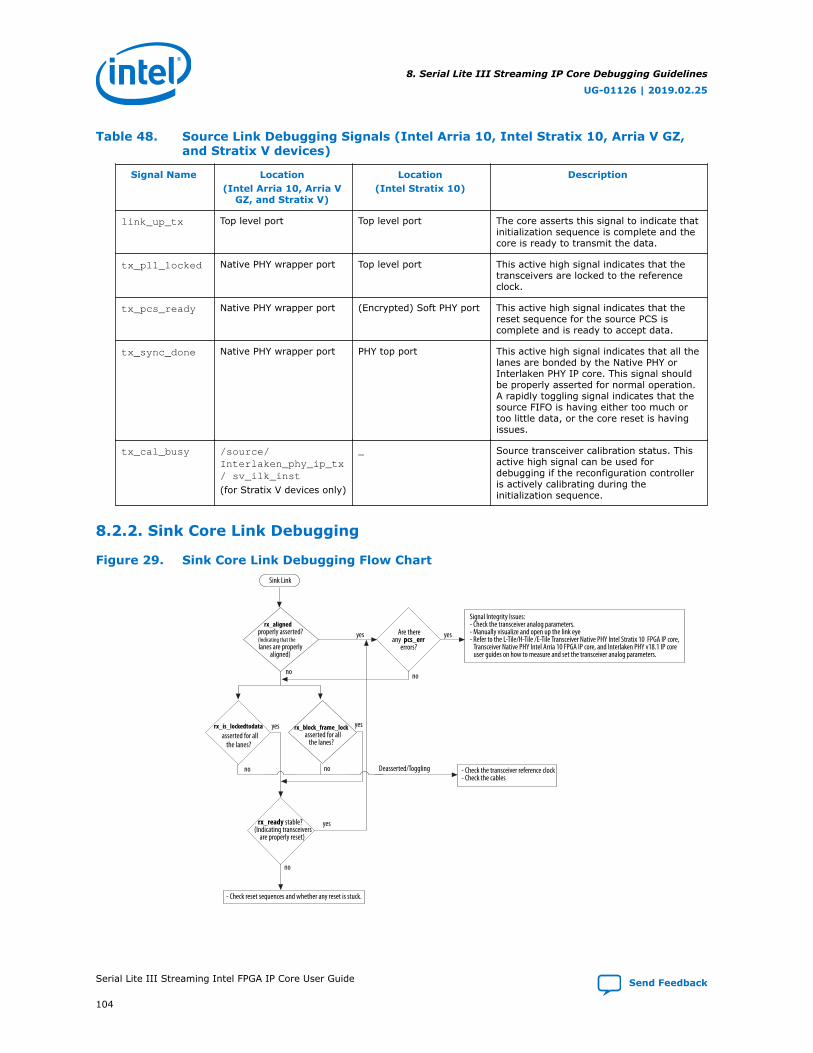
Table 48. Source Link Debugging Signals (Intel Arria 10, Intel Stratix 10, Arria V GZ,and Stratix V devices)
Signal Name Location(Intel Arria 10, Arria V
GZ, and Stratix V)
Location(Intel Stratix 10)
Description
link_up_tx Top level port Top level port The core asserts this signal to indicate thatinitialization sequence is complete and thecore is ready to transmit the data.
tx_pll_locked Native PHY wrapper port Top level port This active high signal indicates that thetransceivers are locked to the referenceclock.
tx_pcs_ready Native PHY wrapper port (Encrypted) Soft PHY port This active high signal indicates that thereset sequence for the source PCS iscomplete and is ready to accept data.
tx_sync_done Native PHY wrapper port PHY top port This active high signal indicates that all thelanes are bonded by the Native PHY orInterlaken PHY IP core. This signal shouldbe properly asserted for normal operation.A rapidly toggling signal indicates that thesource FIFO is having either too much ortoo little data, or the core reset is havingissues.
tx_cal_busy /source/Interlaken_phy_ip_tx/ sv_ilk_inst
(for Stratix V devices only)
_ Source transceiver calibration status. Thisactive high signal can be used fordebugging if the reconfiguration controlleris actively calibrating during theinitialization sequence.
8.2.2. Sink Core Link Debugging
Figure 29. Sink Core Link Debugging Flow ChartSink Link
rx_alignedproperly asserted?(Indicating that thelanes are properly
aligned)
yes
no
Are thereany pcs_err
errors?
yes
no
rx_block_frame_lockasserted for all
the lanes?
yes
no Deasserted/Toggling
rx_ready stable?(Indicating transceivers
are properly reset)
no
rx_is_lockedtodataasserted for all
the lanes?
yes
no
Signal Integrity Issues:- Check the transceiver analog parameters.- Manually visualize and open up the link eye - Refer to the L-Tile/H-Tile /E-Tile Transceiver Native PHY Intel Stratix 10 FPGA IP core, Transceiver Native PHY Intel Arria 10 FPGA IP core, and Interlaken PHY v18.1 IP core user guides on how to measure and set the transceiver analog parameters.
yes
- Check the transceiver reference clock- Check the cables
- Check reset sequences and whether any reset is stuck.
8. Serial Lite III Streaming IP Core Debugging Guidelines
UG-01126 | 2019.02.25
Serial Lite III Streaming Intel FPGA IP Core User Guide Send Feedback
104
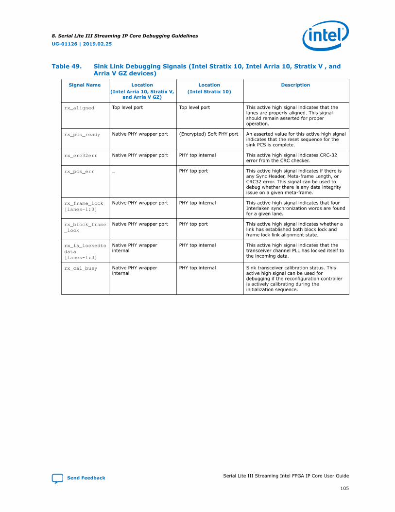
Table 49. Sink Link Debugging Signals (Intel Stratix 10, Intel Arria 10, Stratix V , andArria V GZ devices)
Signal Name Location(Intel Arria 10, Stratix V,
and Arria V GZ)
Location(Intel Stratix 10)
Description
rx_aligned Top level port Top level port This active high signal indicates that thelanes are properly aligned. This signalshould remain asserted for properoperation.
rx_pcs_ready Native PHY wrapper port (Encrypted) Soft PHY port An asserted value for this active high signalindicates that the reset sequence for thesink PCS is complete.
rx_crc32err Native PHY wrapper port PHY top internal This active high signal indicates CRC-32error from the CRC checker.
rx_pcs_err _ PHY top port This active high signal indicates if there isany Sync Header, Meta-frame Length, orCRC32 error. This signal can be used todebug whether there is any data integrityissue on a given meta-frame.
rx_frame_lock[lanes-1:0]
Native PHY wrapper port PHY top internal This active high signal indicates that fourInterlaken synchronization words are foundfor a given lane.
rx_block_frame_lock
Native PHY wrapper port PHY top port This active high signal indicates whether alink has established both block lock andframe lock link alignment state.
rx_is_lockedtodata[lanes-1:0]
Native PHY wrapperinternal
PHY top internal This active high signal indicates that thetransceiver channel PLL has locked itself tothe incoming data.
rx_cal_busy Native PHY wrapperinternal
PHY top internal Sink transceiver calibration status. Thisactive high signal can be used fordebugging if the reconfiguration controlleris actively calibrating during theinitialization sequence.
8. Serial Lite III Streaming IP Core Debugging Guidelines
UG-01126 | 2019.02.25
Send Feedback Serial Lite III Streaming Intel FPGA IP Core User Guide
105
9. Serial Lite III Streaming IP Core User Guide ArchivesIf an IP core version is not listed, the user guide for the previous IP core version applies.
IP Core Version User Guide
18.1 SerialLite III Streaming IP Core User Guide
18.0 SerialLite III Streaming IP Core User Guide
17.1 SerialLite III Streaming IP Core User Guide
17.0 SerialLite III Streaming IP Core User Guide
16.1 SerialLite III Streaming IP Core User Guide
16.0 SerialLite III Streaming IP Core User Guide
15.1 SerialLite III Streaming IP Core User Guide
15.0 SerialLite III Streaming IP Core User Guide
14.1 SerialLite III Streaming IP Core User Guide
UG-01126 | 2019.02.25
Send Feedback
Intel Corporation. All rights reserved. Intel, the Intel logo, Altera, Arria, Cyclone, Enpirion, MAX, Nios, Quartusand Stratix words and logos are trademarks of Intel Corporation or its subsidiaries in the U.S. and/or othercountries. Intel warrants performance of its FPGA and semiconductor products to current specifications inaccordance with Intel's standard warranty, but reserves the right to make changes to any products and servicesat any time without notice. Intel assumes no responsibility or liability arising out of the application or use of anyinformation, product, or service described herein except as expressly agreed to in writing by Intel. Intelcustomers are advised to obtain the latest version of device specifications before relying on any publishedinformation and before placing orders for products or services.*Other names and brands may be claimed as the property of others.
ISO9001:2015Registered

10. Document Revision History for the Intel FPGA SerialLite III Streaming IP Core User Guide
Document Version Intel QuartusPrime Version
Changes
2019.02.25 18.1.1 Added Intel Stratix 10 E-Tile Transceiver PHY User Guide: PMA Adaptationlink in the Parameter Settings for Intel Stratix 10 Devices topic, to providemore information on parameters in the PMA Adaptation tab.
2019.01.17 18.1 Updated phy_mgmt_addr signal description for Intel Stratix 10 device inL-Tile/H-Tile/E-Tile Transceiver Native PHY Intel Stratix 10 IP Core Signals(Interlaken Mode) table.
2018.09.24 18.1 • Updated resource utilization with E-tile transceiver support.• Added Serial Lite III Streaming Intel FPGA IP Transceiver Tiles Support
in Intel Stratix 10 Devices table.• Added note to clarify parameters that are not supported in E-tile
transceiver.• Added the following registers in Source Configuration and Status
Registers for MAC and Sink Configuration and Status Registers for MACtables:— TX MAC Status— RX MAC Status
• Removed the following bits in Sink Configuration and Status Registersfor MAC table:— RX Loss of Frame Lock Consolidated Status bit 2 of RX Error Status
Register— RX Loss of Frame Lock Interrupt bit 2 of RX Error Interrupt Enable
Register• Added the following bits in Sink Configuration and Status Registers for
MAC table:— RX Data Error bit 11 of RX Error Status Register— RX Adaptation FIFO Overflow bit 7 of RX Error Status Register— RX Data Error Enable bit 11 of RX Error Interrupt Enable Register— RX Adaptation FIFO Overflow Enable bit 7 of RX Error Interrupt
Enable Register• Added a note to clarify that Riviera Pro is not supported for E-tile
transceiver.• Updated Error Detection, Reporting, and Recovering Mechanism topic
with reporting and recovering mechanisms.• Updated core latency for Intel Stratix 10 E-tile transceiver devices in
Latency Measurement for Duplex Core table.
continued...
UG-01126 | 2019.02.25
Send Feedback
Intel Corporation. All rights reserved. Intel, the Intel logo, Altera, Arria, Cyclone, Enpirion, MAX, Nios, Quartusand Stratix words and logos are trademarks of Intel Corporation or its subsidiaries in the U.S. and/or othercountries. Intel warrants performance of its FPGA and semiconductor products to current specifications inaccordance with Intel's standard warranty, but reserves the right to make changes to any products and servicesat any time without notice. Intel assumes no responsibility or liability arising out of the application or use of anyinformation, product, or service described herein except as expressly agreed to in writing by Intel. Intelcustomers are advised to obtain the latest version of device specifications before relying on any publishedinformation and before placing orders for products or services.*Other names and brands may be claimed as the property of others.
ISO9001:2015Registered

Document Version Intel QuartusPrime Version
Changes
• Added Intel Stratix 10 E-tile transceiver devices standard and advancedclocking mode block diagrams.
• Updated reset scheme for Intel Stratix 10 E-tile transceiver devices.• Added IP core link up sequences with waveforms in Link-Up Sequence
topic.
2018.05.07 18.0 • Updated 28 Gbps with 4 data lanes support for Intel Stratix 10 devices.• Updated resources for 28 Gbps with 4 data lanes in SerialLite III
Streaming IP Core Performance and Resource Utilization table.• Reorganized SerialLite III Streaming IP Core Functional Description and
SerialLite III Streaming IP Core Clocking Guidelines chapters.• Added SerialLite III Streaming Intel FPGA IP Core Design Examples
section.
Date Version Changes
December 2017 2017.12.27 • Updated transceiver data rate from 25 Gbps to 17.4 Gbps for GXTselection in Transceiver Channel Typeparameter.
November 2017 2017.11.06 • Updated parameter settings for Intel Stratix 10, , and Stratix V andArria V GZ devices.
• Updated transfer data rate supported in Intel Stratix 10 devices.• Added performance, transceiver speed grade and resource utilization
for 25 and 28 Gbps data rate for Intel Stratix 10 devices.• Added a note to specify no support for simplex receiver mode in Intel
Stratix 10 devices for data rate greater than 17.4 Gbps.
May 2017 2017.05.08 • Clarified the device family support for Intel Stratix 10 devices.• Clarified the exact replica of output data support for pure streaming
operation in the following locations:— Continuous Mode sub-topic— IP Core Architecture topic— Comparing Standard and Advanced Clocking Modes table— Standard Clocking Mode sub-topic— Sink Adaptation Module sub-topic— Standard Clocking Mode vs Advanced Clocking Mode topic
• Removed the Continuous vs. Burst Mode Characteristics table.• Updated the SerialLite III Streaming IP Core FPGA Performance and
Resource Utilization table for Intel Arria 10, Stratix V GX and Arria VGZ, and Intel Stratix 10 devices.
• Updated the SerialLite III Streaming IP Core Parameters table:— Removed the Streaming Mode parameter.— Updated the description for User input parameter.
• Updated the description in the Specifying IP Core Parameters andOptions topic.
• Updated the Simulation Parameters sub-topic to include testbenchdefault simulation parameters for Intel Arria 10 and Intel Stratix 10devices.
• Updated the Simulator column in the Intel FPGA IP Core SimulationScripts table.
• Updated the Interlaken PHY IP Duplex Core or Native PHY IP DuplexCore - Interlaken Mode topic.
• Updated the description of the phy_mgmt_clk signal in the SerialLiteIII Streaming IP Core Clock Domains and Signals table.
• Updated the SerialLite III Streaming Sink Core topic.• Updated the Latency Measurement for Duplex Core table in the Core
Latency topic to include Intel Stratix 10 device.• Updated the second note in the Reset topic.
continued...
10. Document Revision History for the Intel FPGA Serial Lite III Streaming IP Core User Guide
UG-01126 | 2019.02.25
Serial Lite III Streaming Intel FPGA IP Core User Guide Send Feedback
108

Date Version Changes
• Updated the description in the CRC-32 Error Injection topic.• Updated the Clocking Structure for Stratix 10 Devices topic:
— Added the Source and Sink descriptions for interface_clock signalin the Intel Stratix 10 Clocks in Standard Clocking Mode table.
— Added tx_clkout and rx_clkout signals in the Intel Stratix 10Clocks in Advanced Clocking Mode table.
— Updated the description for Choosing TX PLL Type for Intel Stratix10 Devices sub-topic.
• Updated the Clocking Structure For Intel Arria 10 Devices topic:— Updated the Clocking Structure for Intel Arria 10 Devices figure.— Updated the Source and Sink descriptions for interface_clock
signal in the Intel Arria 10 Clocks in Standard Clocking Modetable.
— Updated the description for Choosing TX PLL Type for Intel Arria10 Devices sub-topic.
• Updated the SerialLite III Streaming Link Debugging topic:— Updated the Source Core Link Debugging Flow Chart figure.— Updated the Source Link Debugging Signals table to include Intel
Stratix 10 support.— Updated the Sink Core Link Debugging Flow Chart figure.— Updated the Sink Link Debugging Signals table to include Intel
Stratix 10 support.• Updated the Error Handling topic:
— Updated the sink core error flag.— Added information on error status on error_rx signal condition.
• Updated the Register Map for SerialLite III Streaming MAC table:— Added RX Error Status register.— Updated the source register name for 0x0090 from TX Error to TX
Error Status.— Removed RX MAC status.
• Updated the Configuration and Status Registers topic.• Minor typographical corrections and stylistic changes.
October 2016 2016.10.28 • Added information about Intel Stratix 10 support.• Update document template.
May 2016 2016.05.02 • Added a new parameter—Enable Transceiver Native PHY ADME• Updated the IP core parameter names.• Added new sections:
— Serial Lite III Streaming IP Core Clocking Guidelines on page 75— Creating a Signal Tap Debug File to Match Your Design Hierarchy
on page 102• Revised the core_reset signal description—removed 32-cycle reset
restriction. This restriction is removed in IP core version 15.1onwards but is still applicable to prior versions.
• Updated the IP Core release information.• Removed the design example chapter. The information is now located
in the Design Examples for SerialLite III Streaming IP Core UserGuide.
November 2015 2015.11.02 • Updated the IP Core Performance and Resource Utilization table.• Added a new topic—Intel FPGA IP Evaluation Mode Timeout Behavior
on page 15• Added a link to Introduction to Altera IP Cores.• Added a note in "Altera IP Core Simulation Scripts" to recommend
that you run the msim_setup.tcl script in the ModelSim-AlteraSimulator Tcl console.
• Changed the minimum required gap between bursts to one userclock cycle.
continued...
10. Document Revision History for the Intel FPGA Serial Lite III Streaming IP Core User Guide
UG-01126 | 2019.02.25
Send Feedback Serial Lite III Streaming Intel FPGA IP Core User Guide
109

Date Version Changes
• Added information about using I/O PLL to generate the core clockand user clock signals for Arria 10 devices.
• Added a new parameter—Burst Gap.• Updated the parameter description for Interface clock frequency,
Core clock frequency, and fPLL reference clock frequency.• Updated the parameter value for Core clock frequency.• Updated the PMA width for Interlaken mode to 64 bits for Arria 10
devices.• Updated all SerialLite III Streaming IP Core block diagrams.• Removed the Source PPM Absorption module from the core.• Changed the bit function and description for error (source core) and
error_tx (duplex core) signals.• Updated the description of link_up_rx signal.• Added "Interlaken PHY Register Descriptions" table to specify the
registers to access using the Avalon-MM PHY management interface.• Updated the design example to support Arria 10 devices.• Changed the target development kit to Transceiver Signal Integrity
Development Kit, Stratix V GX Edition.• Updated the design operation names in the Design Example
Operation topic.• Changed the sink link debug signal from rx_crc32 to
rx_crc32err.• Updated the sink core conditions in the Error Handling topic.• Changed instances of Quartus II to Quartus Prime.
May 2015 2015.05.04 • Updated the IP Core Performance and Resource Utilization table.• Changed the width of sync_rx and sync_tx signals from 4 to 8 bits
in Signals.• Added external serial loopback in Testbench and Testbench.
December 2014 2014.12.15 Described Arria 10 support for up to 17.4 Gbps transceiver data rate.Updated core latency numbers. Updated the Transmission Overheadsand Lane Rate Calculations on page 39. Minor text changes.
August 2014 2014.08.18 Added information about Arria 10 support.
June 2014 2014.06.30 Replaced references to MegaWizard Plug-In Manager with IP catalog orparameter editor. Minor text changes.
November 2013 2013.11.04 • Added information on CRC-32 error injection.• Added information on the FIFO ECC protection option.
May 2013 2013.05.13 Initial release
10. Document Revision History for the Intel FPGA Serial Lite III Streaming IP Core User Guide
UG-01126 | 2019.02.25
Serial Lite III Streaming Intel FPGA IP Core User Guide Send Feedback
110