Embed Size (px)
DESCRIPTION
Sequential Timing Optimization. s. i. s. j. T. setup. Long path timing constraints. Data must not reach destination FF too late. d max (i,j). s i + d(i,j) + T setup s j + P. i. j. d(i,j). s. i. s. j. Short path timing constraints. FF should not get >1 data set per period. - PowerPoint PPT Presentation
Citation preview
Sequential Timing Optimization
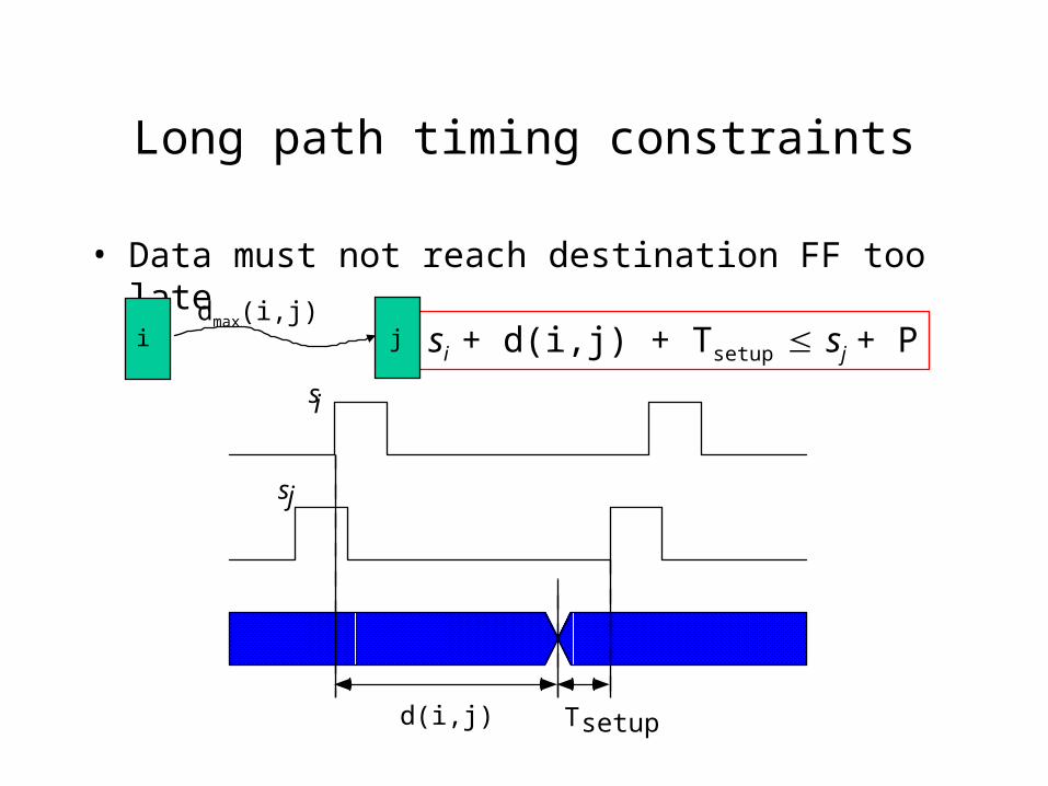
Long path timing constraints
• Data must not reach destination FF too late
si + d(i,j) + Tsetup sj + P
si
sj
d(i,j) T setup
dmax(i,j)i j
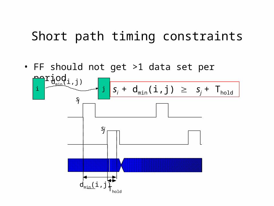
Short path timing constraints
• FF should not get >1 data set per period
si
sj
dmin(i,j) Thold
si + dmin(i,j) sj + Thold
dmin(i,j)i j
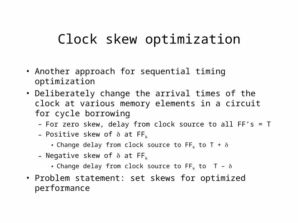
Clock skew optimization
• Another approach for sequential timing optimization
• Deliberately change the arrival times of the clock at various memory elements in a circuit for cycle borrowing– For zero skew, delay from clock source to all FF’s = T
– Positive skew of at FFk
• Change delay from clock source to FFk to T +
– Negative skew of at FFk
• Change delay from clock source to FFk to T –
• Problem statement: set skews for optimized performance
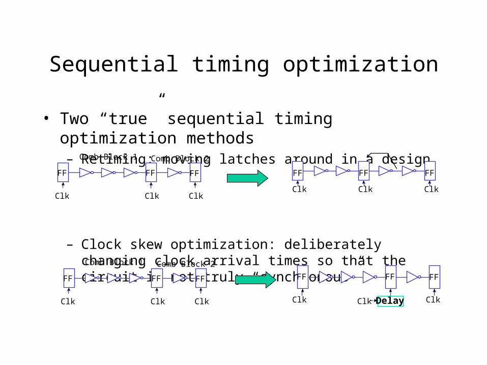
Sequential timing optimization
• Two “true” sequential timing optimization methods– Retiming: moving latches around in a design
– Clock skew optimization: deliberately changing clock arrival times so that the circuit is not truly “synchronous”
Clk Clk
Comb Block 1 Comb Block 2
Clk
FF FF FF FF
Clk
FF FF
Clk Clk
ClkClk
FF FF FF
DelayClkClk Clk
Comb Block 1 Comb Block 2
Clk
FF FF FF
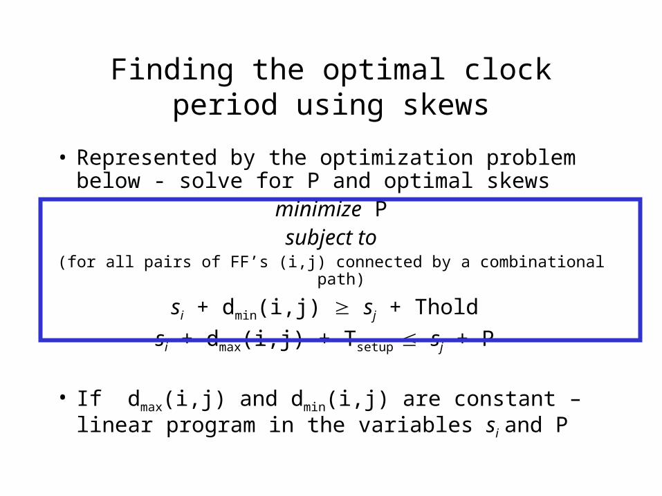
• Represented by the optimization problem below - solve for P and optimal skews
minimize Psubject to
(for all pairs of FF’s (i,j) connected by a combinational path)
si + dmin(i,j) sj + Thold
si + dmax(i,j) + Tsetup sj + P
• If dmax(i,j) and dmin(i,j) are constant – linear program in the variables si and P
Finding the optimal clock period using skews
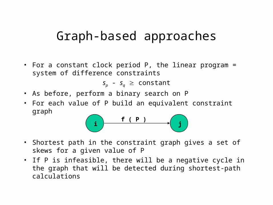
Graph-based approaches
• For a constant clock period P, the linear program = system of difference constraints
sp - sq constant
• As before, perform a binary search on P
• For each value of P build an equivalent constraint graph
• Shortest path in the constraint graph gives a set of skews for a given value of P
• If P is infeasible, there will be a negative cycle in the graph that will be detected during shortest-path calculations
i jf ( P )

Retiming
Assume unit gate delays, no setup times
Initial Circuit: P=3
Retimed Circuit: P=2
Clk Clk
Comb Block 1 Comb Block 2
Clk
FF FF FF
FF
Clk
FF FF
Clk Clk
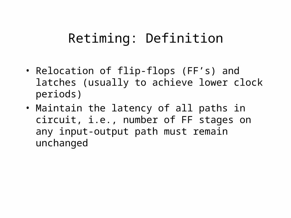
Retiming: Definition
• Relocation of flip-flops (FF’s) and latches (usually to achieve lower clock periods)
• Maintain the latency of all paths in circuit, i.e., number of FF stages on any input-output path must remain unchanged
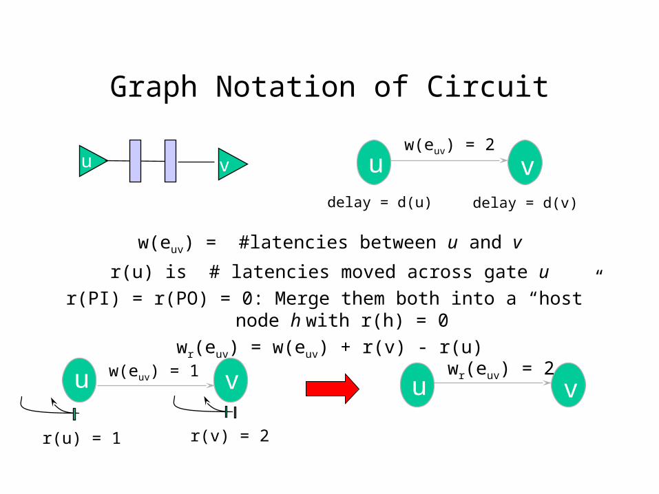
Graph Notation of Circuit
w(euv) = #latencies between u and v
r(u) is # latencies moved across gate u
r(PI) = r(PO) = 0: Merge them both into a “host” node h with r(h) = 0
wr(euv) = w(euv) + r(v) - r(u)
u vw(euv) = 2
r(u) = 1
w(euv) = 1u v
r(v) = 2
u vwr(euv) = 2
u v
delay = d(u) delay = d(v)
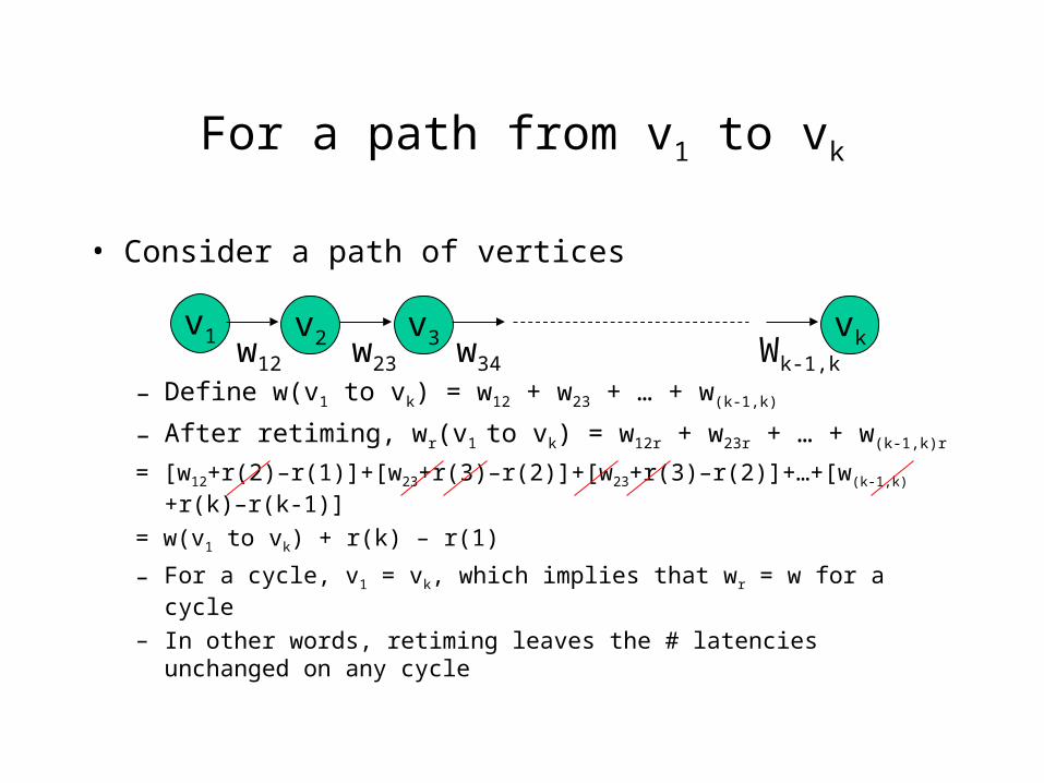
For a path from v1 to vk
• Consider a path of vertices
– Define w(v1 to vk) = w12 + w23 + … + w(k-1,k)
– After retiming, wr(v1 to vk) = w12r + w23r + … + w(k-1,k)r
= [w12+r(2)–r(1)]+[w23+r(3)–r(2)]+[w23+r(3)–r(2)]+…+[w(k-1,k)+r(k)–r(k-1)]
= w(v1 to vk) + r(k) – r(1)
– For a cycle, v1 = vk, which implies that wr = w for a cycle
– In other words, retiming leaves the # latencies unchanged on any cycle
v1 v2 v3 vkw12 w23 w34 Wk-1,k
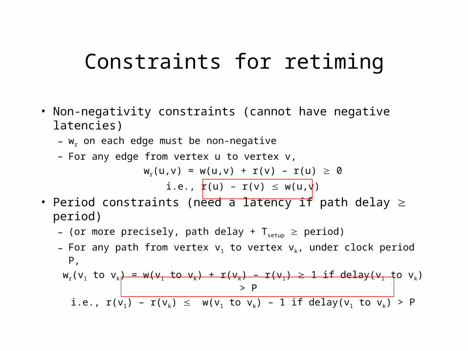
Constraints for retiming
• Non-negativity constraints (cannot have negative latencies)– wr on each edge must be non-negative
– For any edge from vertex u to vertex v,
wr(u,v) = w(u,v) + r(v) – r(u) 0
i.e., r(u) – r(v) w(u,v)
• Period constraints (need a latency if path delay period)– (or more precisely, path delay + Tsetup period)
– For any path from vertex v1 to vertex vk, under clock period P,
wr(v1 to vk) = w(v1 to vk) + r(vk) – r(v1) 1 if delay(v1 to vk) > P
i.e., r(v1) – r(vk) w(v1 to vk) – 1 if delay(v1 to vk) > P
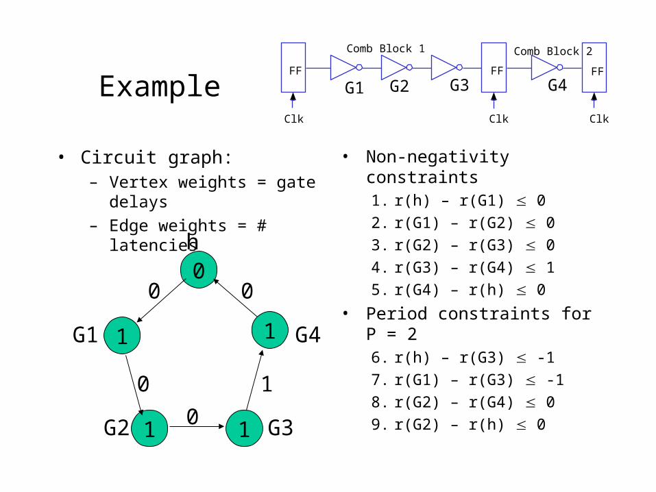
Example
• Circuit graph:– Vertex weights = gate delays
– Edge weights = # latencies
• Non-negativity constraints1. r(h) – r(G1) 0
2. r(G1) – r(G2) 0
3. r(G2) – r(G3) 0
4. r(G3) – r(G4) 1
5. r(G4) – r(h) 0
• Period constraints for P = 26. r(h) – r(G3) -1
7. r(G1) – r(G3) -1
8. r(G2) – r(G4) 0
9. r(G2) – r(h) 0
Clk Clk
Comb Block 1 Comb Block 2
Clk
FF FF FF
G1 G3G2 G4
0
11
1 1
0 0
1
0
0
G1
G2 G3
G4
h
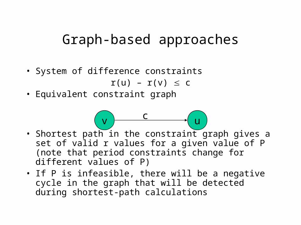
Graph-based approaches
• System of difference constraintsr(u) – r(v) c
• Equivalent constraint graph
• Shortest path in the constraint graph gives a set of valid r values for a given value of P (note that period constraints change for different values of P)
• If P is infeasible, there will be a negative cycle in the graph that will be detected during shortest-path calculations
v uc
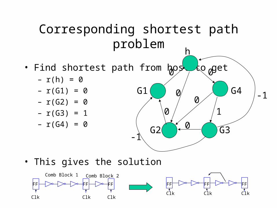
Corresponding shortest path problem
• Find shortest path from host to get– r(h) = 0
– r(G1) = 0
– r(G2) = 0
– r(G3) = 1
– r(G4) = 0
• This gives the solution
0 0
1
0
0
G1
G2 G3
G4
h
-1
-1
00
Clk Clk
Comb Block 1 Comb Block 2
Clk
FF FF FF FF
Clk
FF FF
Clk Clk
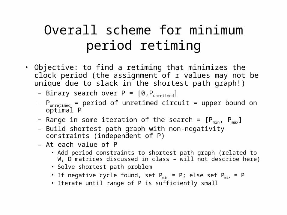
Overall scheme for minimum period retiming
• Objective: to find a retiming that minimizes the clock period (the assignment of r values may not be unique due to slack in the shortest path graph!)– Binary search over P = [0,Punretimed]– Punretimed = period of unretimed circuit = upper bound on optimal P– Range in some iteration of the search = [Pmin, Pmax]– Build shortest path graph with non-negativity constraints (independent of
P)– At each value of P
• Add period constraints to shortest path graph (related to W, D matrices discussed in class – will not describe here)
• Solve shortest path problem• If negative cycle found, set Pmin = P; else set Pmax = P• Iterate until range of P is sufficiently small
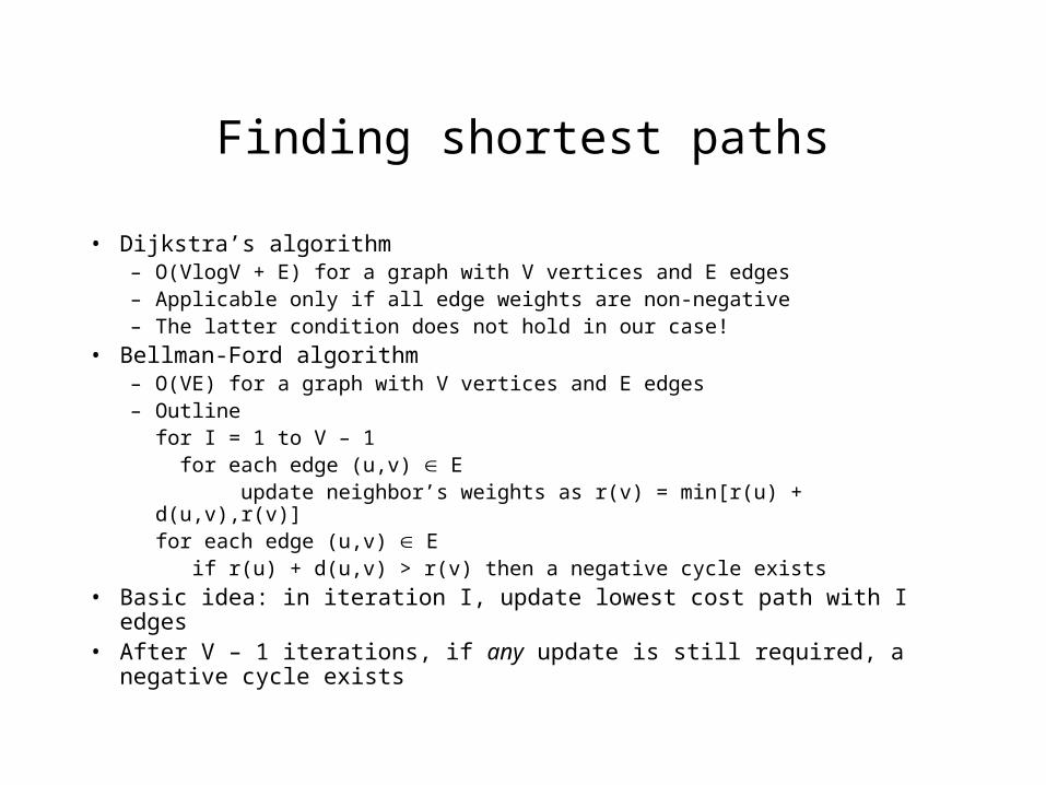
Finding shortest paths
• Dijkstra’s algorithm– O(VlogV + E) for a graph with V vertices and E edges– Applicable only if all edge weights are non-negative– The latter condition does not hold in our case!
• Bellman-Ford algorithm– O(VE) for a graph with V vertices and E edges– Outline
for I = 1 to V – 1 for each edge (u,v) E update neighbor’s weights as r(v) = min[r(u) + d(u,v),r(v)]
for each edge (u,v) E if r(u) + d(u,v) > r(v) then a negative cycle exists
• Basic idea: in iteration I, update lowest cost path with I edges• After V – 1 iterations, if any update is still required, a negative cycle exists
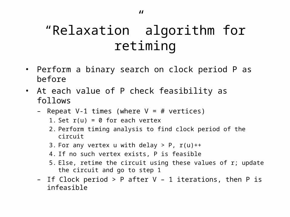
“Relaxation” algorithm for retiming
• Perform a binary search on clock period P as before
• At each value of P check feasibility as follows– Repeat V-1 times (where V = # vertices)
1. Set r(u) = 0 for each vertex
2. Perform timing analysis to find clock period of the circuit
3. For any vertex u with delay > P, r(u)++
4. If no such vertex exists, P is feasible
5. Else, retime the circuit using these values of r; update the circuit and go to step 1
– If Clock period > P after V – 1 iterations, then P is infeasible
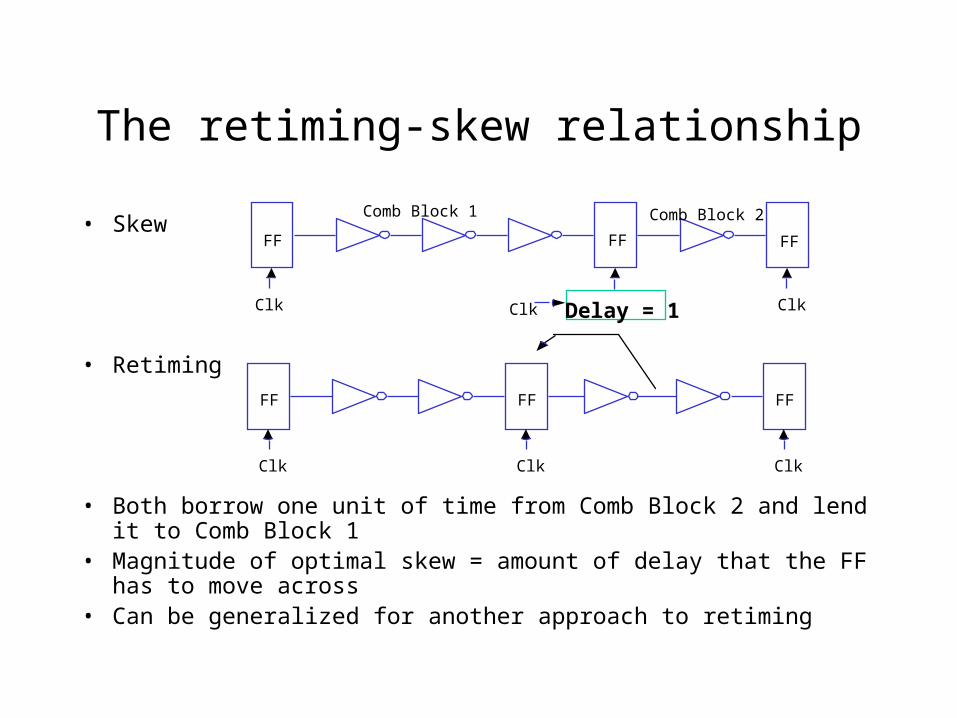
The retiming-skew relationship
• Skew
• Retiming
• Both borrow one unit of time from Comb Block 2 and lend it to Comb Block 1
• Magnitude of optimal skew = amount of delay that the FF has to move across
• Can be generalized for another approach to retiming
FF
Clk
FF FF
Clk Clk
Clk
Comb Block 1 Comb Block 2
Clk
FF FF FF
Delay = 1Clk
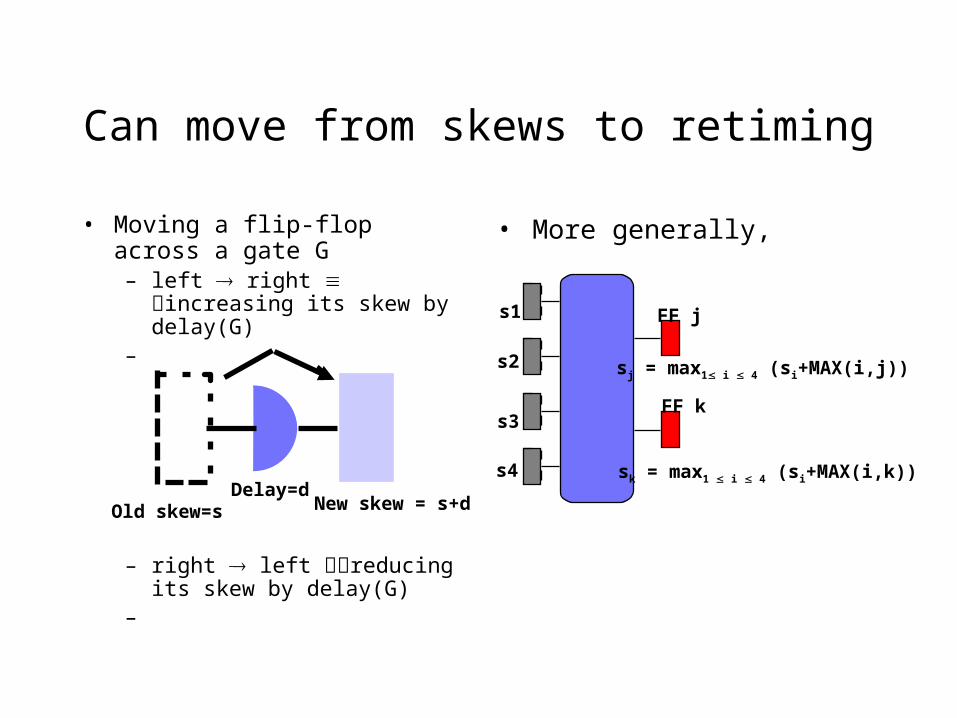
Can move from skews to retiming
• Moving a flip-flop across a gate G– left right increasing its
skew by delay(G)–
– right left reducing its skew by delay(G)
–
• More generally,
Old skew=sDelay=d
New skew = s+d
s1
s2
s3
s4
sj = max1 i 4 (si+MAX(i,j))
sk = max1 i 4 (si+MAX(i,k))
FF j
FF k
Another approach to retiming
• Two-phase approach– Phase A: Find optimal skews
(complexity depends on the number of FF’s, not the number of gates)
– Phase B: Relocate FF’s to retime circuit(since most FF movements are seen to be local in practice, this does not
take too long)
– Not provably better than earlier approach in terms of complexity, but practically works very well