Embed Size (px)
Citation preview
Sequential Logic
Design:
Controllers
Controller Design,
Flip Flop Timing
Copyright (c) 2012 Sean Key
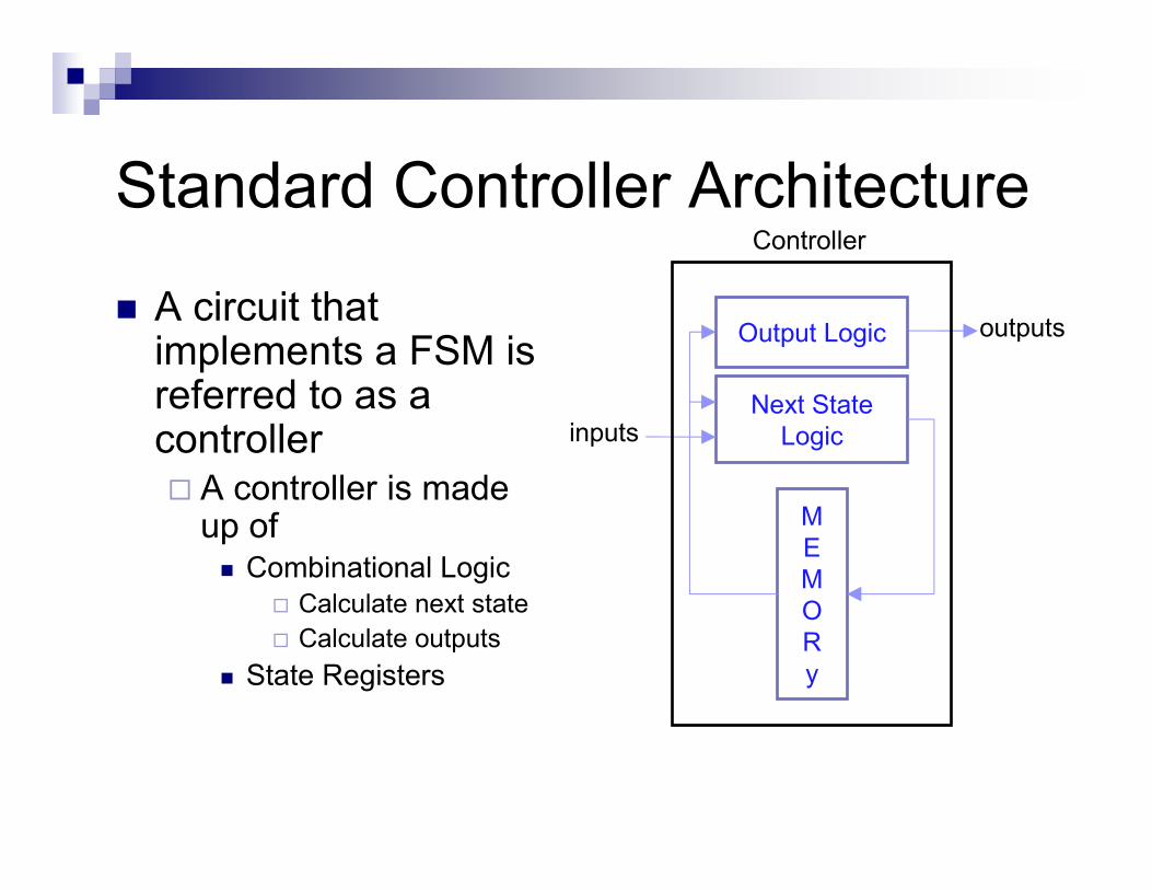
Standard Controller Architecture
� A circuit that implements a FSM is referred to as a controller� A controller is made
up of� Combinational Logic
� Calculate next state
� Calculate outputs
� State Registers
Next State
Logic
M
E
M
O
R
y
inputs
outputs
Controller
Output Logic
Controller Design Process
1. Capture FSM behavior� Create a state diagram to describe the intended behavior
2. Convert to a Circuit1. Set up the standard architecture
� Choose the width of the of the state registers� Determine number of inputs and outputs for the combinational
logic� # circuit inputs� # of state bits
2. Encode the states� Assign unique binary numbers to each state
3. Translate the state diagram into a truth table for the combinational logic.� Order the truth table with state bits first to make it easier to follow
4. Implement the combinational logic from the truth table
Guidelines for Encoding States
� Intelligent selecting of state encodings can simplify the designand/or make it easier to understand and debug.
� Suggested Guidelines:1. Choose an initial code that can be easily forced by a reset (I,e. 000)
2. Minimize the number of state bits that change between transitions.
3. Maximize the number of state bits that don’t change in a group of related transitions.
4. Exploit symmetries in the design� If there are two groups of similar transitions, they should have similar
encodings.
5. If there are unused states, choose the best subset to meet the previous goals.
6. Decompose state variables into individual bits or fields, where each field has a well defined meaning with respect to circuit outputs.
7. Consider using more than the minimum number of state variables to make a decomposed assignment possible.
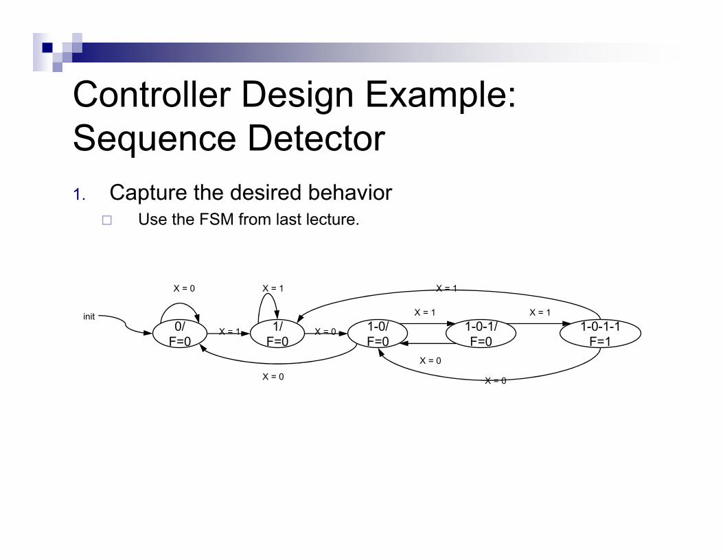
Controller Design Example:
Sequence Detector
1. Capture the desired behavior� Use the FSM from last lecture.
0/
F=0
1/
F=0
1-0/
F=0
1-0-1/
F=0
1-0-1-1
F=1
init
X = 0
X = 1
X = 1
X = 0
X = 1 X = 1
X = 0
X = 0
X = 0
X = 1
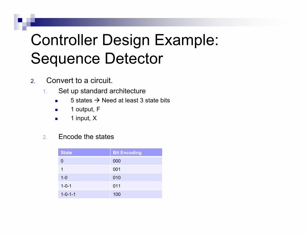
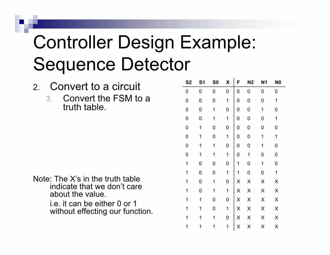
Controller Design Example:
Sequence Detector
2. Convert to a circuit.
1. Set up standard architecture
� 5 states � Need at least 3 state bits
� 1 output, F
� 1 input, X
2. Encode the states
State Bit Encoding
0 000
1 001
1-0 010
1-0-1 011
1-0-1-1 100
Controller Design Example:
Sequence Detector2. Convert to a circuit
3. Convert the FSM to a truth table.
Note: The X’s in the truth table indicate that we don’t care about the value.
i.e. it can be either 0 or 1 without effecting our function.
S2 S1 S0 X F N2 N1 N0
0 0 0 0 0 0 0 0
0 0 0 1 0 0 0 1
0 0 1 0 0 0 1 0
0 0 1 1 0 0 0 1
0 1 0 0 0 0 0 0
0 1 0 1 0 0 1 1
0 1 1 0 0 0 1 0
0 1 1 1 0 1 0 0
1 0 0 0 1 0 1 0
1 0 0 1 1 0 0 1
1 0 1 0 X X X X
1 0 1 1 X X X X
1 1 0 0 X X X X
1 1 0 1 X X X X
1 1 1 0 X X X X
1 1 1 1 X X X X
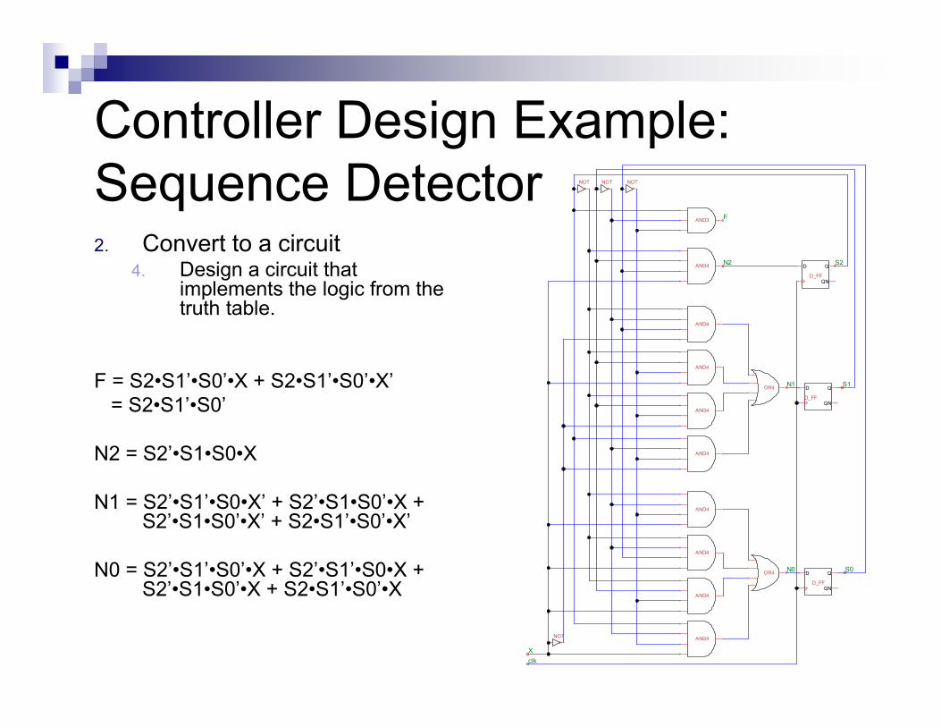
Controller Design Example:
Sequence Detector2. Convert to a circuit
4. Design a circuit that implements the logic from the truth table.
F = S2•S1’•S0’•X + S2•S1’•S0’•X’
= S2•S1’•S0’
N2 = S2’•S1•S0•X
N1 = S2’•S1’•S0•X’ + S2’•S1•S0’•X + S2’•S1•S0’•X’ + S2•S1’•S0’•X’
N0 = S2’•S1’•S0’•X + S2’•S1’•S0•X + S2’•S1•S0’•X + S2•S1’•S0’•X
N0 S0
S1
S2AND4
NOT NOT
NOT
N2
F
NOT
N1
X
clk
AND3
AND4
AND4
AND4
AND4
OR4
OR4
AND4
AND4
AND4
AND4
D Q
QND_FF
D Q
QND_FF
D Q
QND_FF
Reverse Engineering a Circuit
� A FSM can be reverse engineered from a circuit
1. Determine excitation functions from the circuit.
2. Complete a truth table using the excitation functions.
3. Create a FSM from the truth table.� Use generic state names if the operation of the
FSM isn’t immediately apparent.
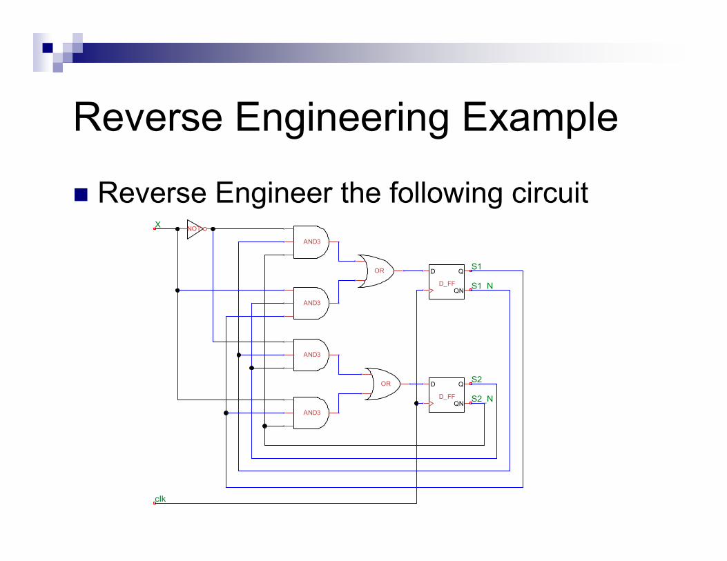
Reverse Engineering Example
� Reverse Engineer the following circuit
D Q
QND_FF
D Q
QND_FF
AND3
AND3
AND3
AND3
OR
OR
X
clk
S1
S1_N
S2
S2_N
NOT
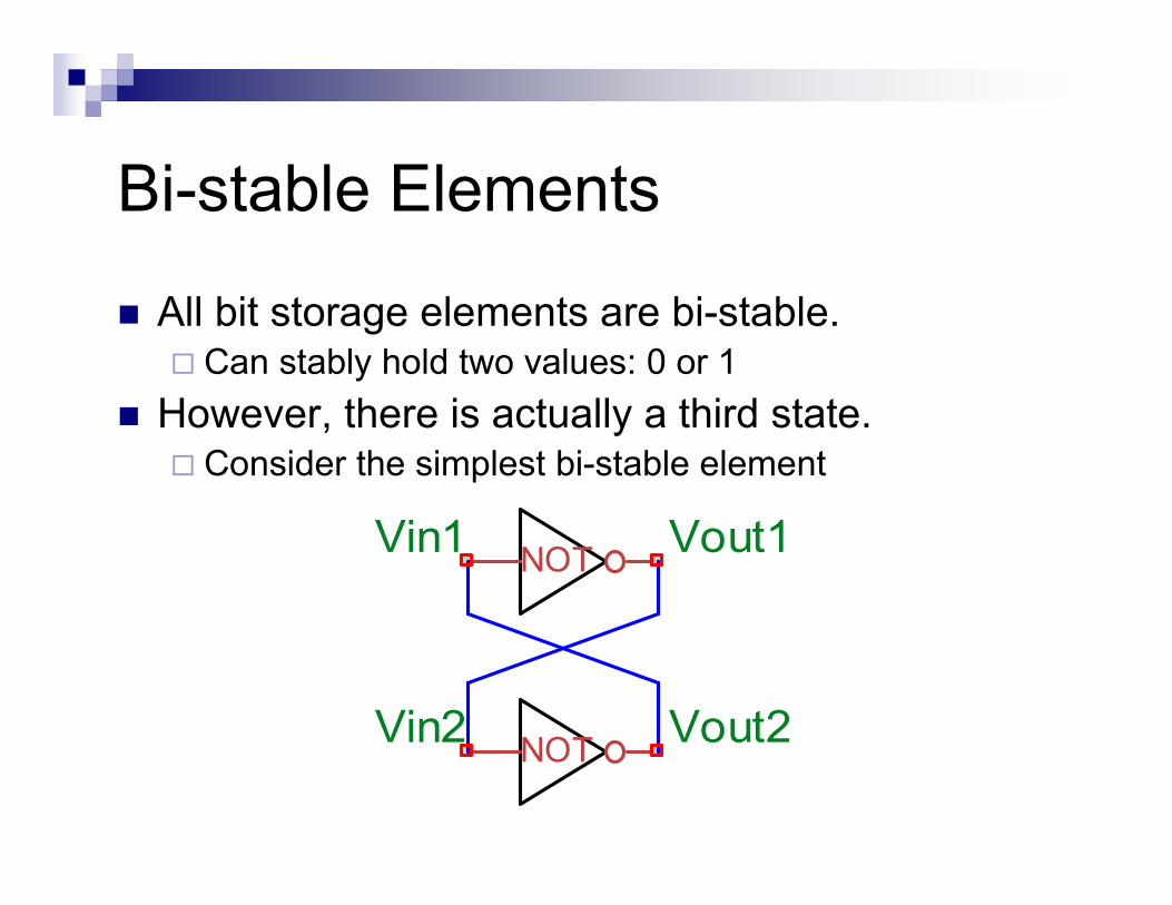
Bi-stable Elements
� All bit storage elements are bi-stable.� Can stably hold two values: 0 or 1
� However, there is actually a third state.� Consider the simplest bi-stable element
NOT
NOT
Vin1
Vin2
Vout1
Vout2
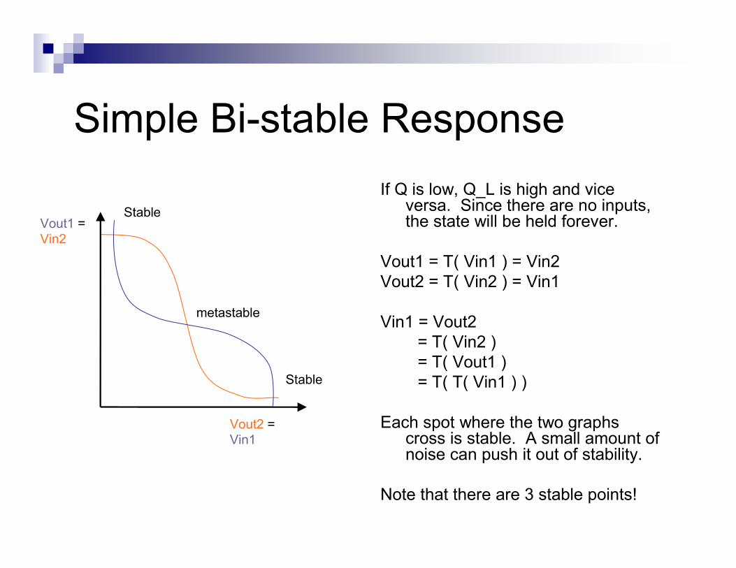
Simple Bi-stable Response
If Q is low, Q_L is high and vice versa. Since there are no inputs, the state will be held forever.
Vout1 = T( Vin1 ) = Vin2
Vout2 = T( Vin2 ) = Vin1
Vin1 = Vout2
= T( Vin2 )
= T( Vout1 )
= T( T( Vin1 ) )
Each spot where the two graphs cross is stable. A small amount of noise can push it out of stability.
Note that there are 3 stable points!
Vout1 =
Vin2
Vout2 =
Vin1
Stable
Stable
metastable
Metastability
� The stable point in the center of the curve is known as metastable� Only slightly stable
� Small amounts of noise cause the outputs to rapidly converge on the truly stable points.
� Because of metastability, it is important to drive
a signal beyond the linear range of the inverter
� Means we have timing requirements for driving gates
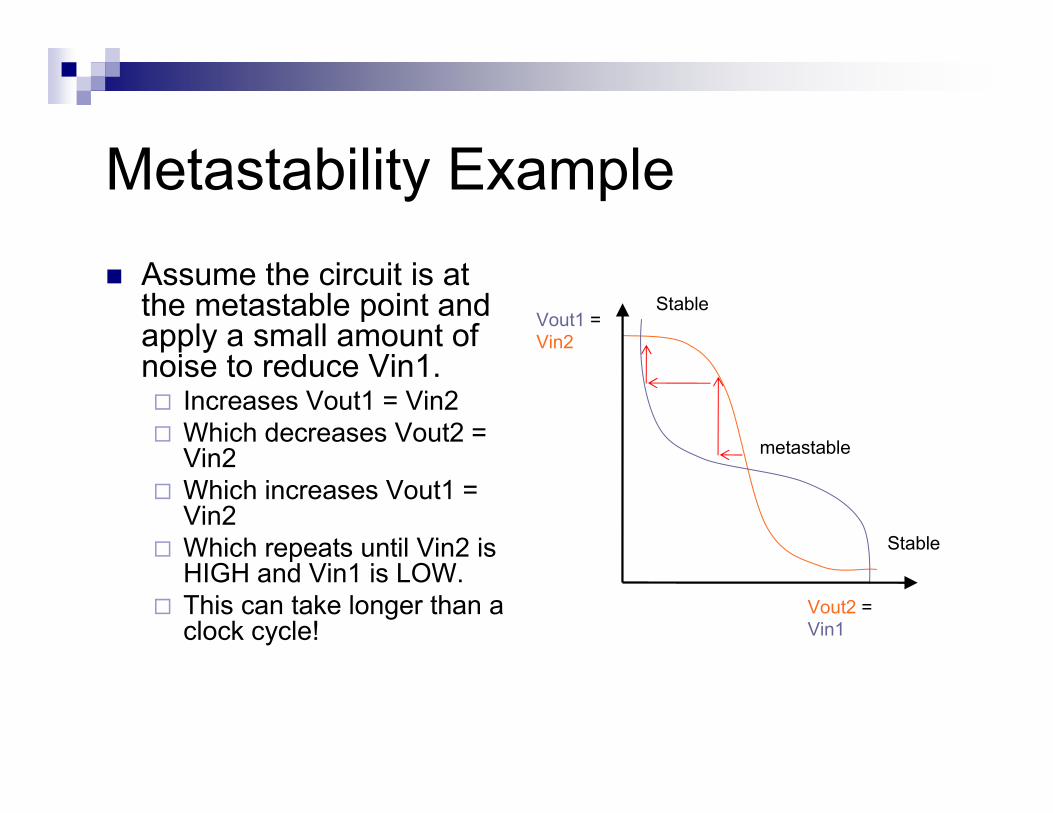
Metastability Example
� Assume the circuit is at the metastable point and apply a small amount of noise to reduce Vin1.� Increases Vout1 = Vin2
� Which decreases Vout2 = Vin2
� Which increases Vout1 = Vin2
� Which repeats until Vin2 is HIGH and Vin1 is LOW.
� This can take longer than a clock cycle!
Vout1 =
Vin2
Vout2 =
Vin1
Stable
Stable
metastable
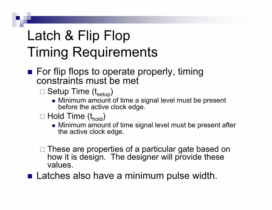
Latch & Flip Flop
Timing Requirements
� For flip flops to operate properly, timing constraints must be met� Setup Time (tsetup)
� Minimum amount of time a signal level must be present before the active clock edge.
� Hold Time (thold)� Minimum amount of time signal level must be present after
the active clock edge.
� These are properties of a particular gate based on how it is design. The designer will provide these values.
� Latches also have a minimum pulse width.
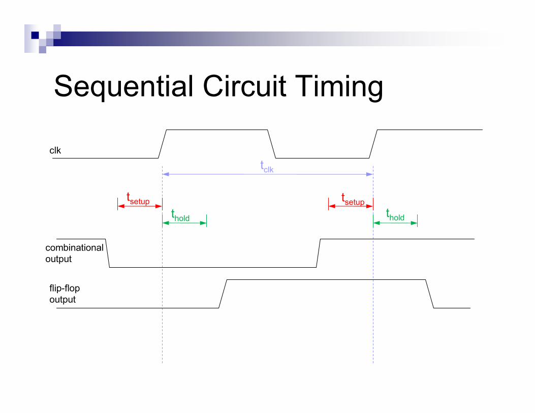
Sequential Circuit Timing
tclk
clk
tsetup tsetup
tholdthold
combinational
output
flip-flop
output
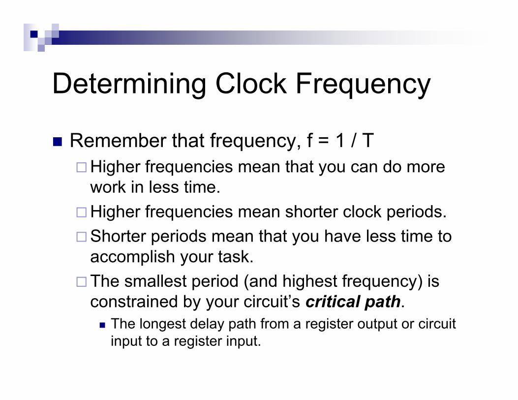
Determining Clock Frequency
� Remember that frequency, f = 1 / T
�Higher frequencies mean that you can do more
work in less time.
�Higher frequencies mean shorter clock periods.
�Shorter periods mean that you have less time to
accomplish your task.
�The smallest period (and highest frequency) is
constrained by your circuit’s critical path.
� The longest delay path from a register output or circuit
input to a register input.
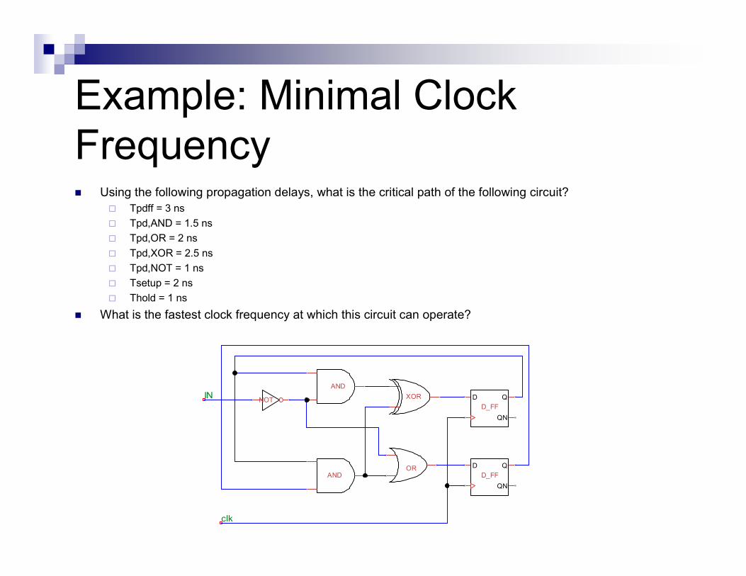
Example: Minimal Clock
Frequency� Using the following propagation delays, what is the critical path of the following circuit?
� Tpdff = 3 ns
� Tpd,AND = 1.5 ns
� Tpd,OR = 2 ns
� Tpd,XOR = 2.5 ns
� Tpd,NOT = 1 ns
� Tsetup = 2 ns
� Thold = 1 ns
� What is the fastest clock frequency at which this circuit can operate?
clk
IN D Q
QN
D_FF
D Q
QN
D_FF
XOR
AND
AND
NOT
OR
Sequential Timing Margins
� Timing margins indicate how much “slop” we have in our timing requirements.� Well designed systems have positive, non-zero margins
� Allows for unexpected timing errors
� Negative margins may lead to metastability.
� Setup-time margin = tclk – tcomb(max) – tsetup – tpd,ff(max)
� Hold-time margin = tffpd(min) + tcomb(min) – thold
� tffpd is almost always larger than thold, so designers rarely evaluate the hold time margin
� Setup-time margins are evaluated for the circuit’s critical path, the longest delay path in the circuit to a flip flop input.
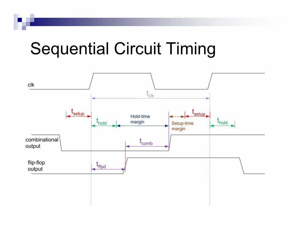
Sequential Circuit Timing
tclk
clk
tsetup tsetup
tholdthold
combinational
output
flip-flop
outputtffpd
tcomb
Setup-time
margin
Hold-time
margin
Timing Diagrams in Sequential
Circuits
� Timing diagrams are done the same as
with combinational logic, but you must
evaluate the circuit for each clock cycle.
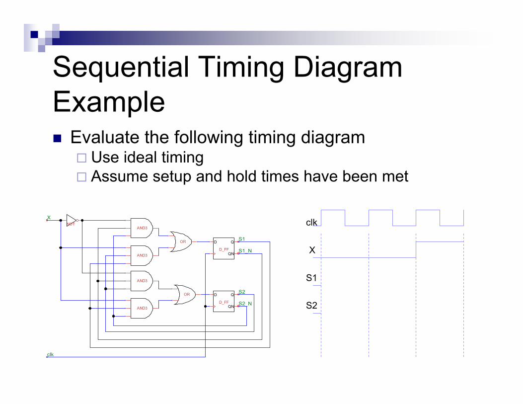
Sequential Timing Diagram
Example� Evaluate the following timing diagram
� Use ideal timing
� Assume setup and hold times have been met
D Q
QND_FF
D Q
QND_FF
AND3
AND3
OR
OR
X
clk
S1
S1_N
S2
S2_N
NOT
AND3
AND3
X
clk
S1
S2
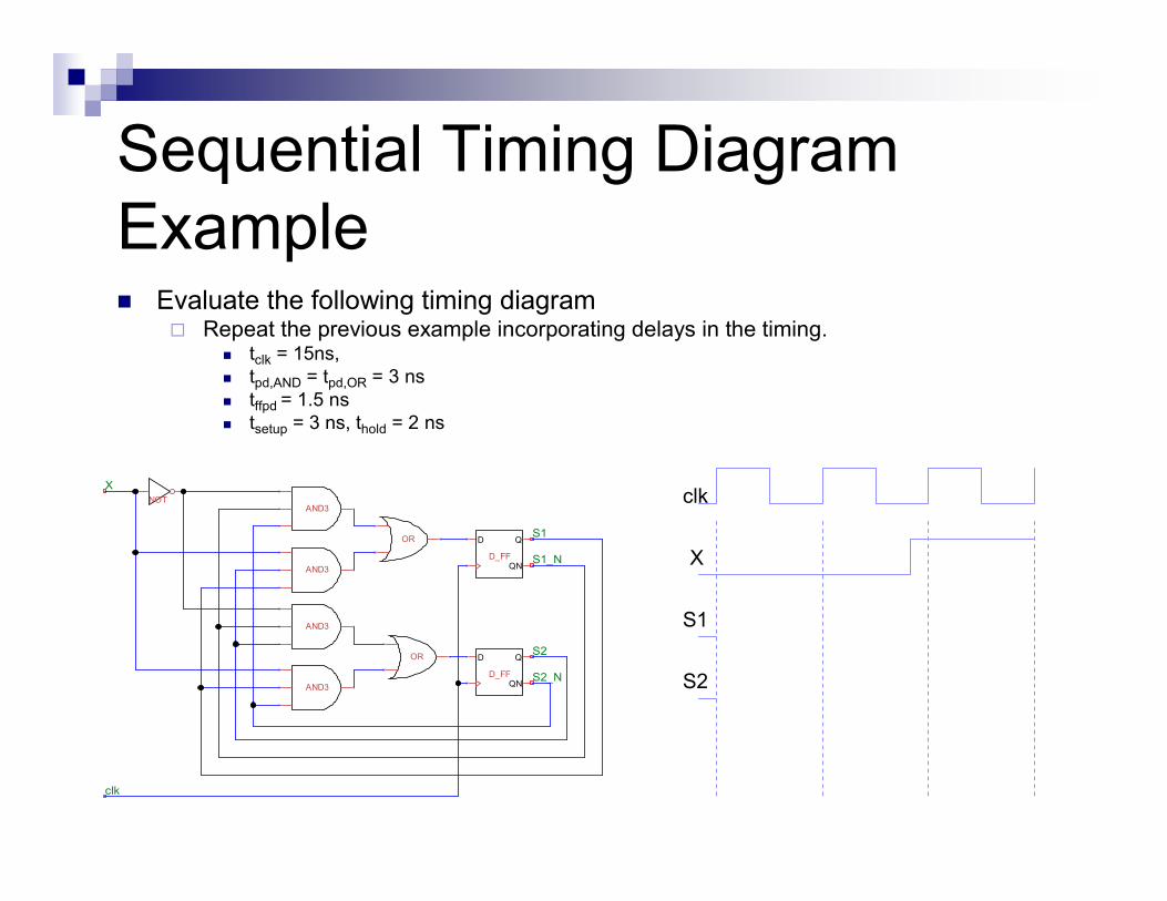
Sequential Timing Diagram
Example� Evaluate the following timing diagram
� Repeat the previous example incorporating delays in the timing.� tclk = 15ns,
� tpd,AND = tpd,OR = 3 ns
� tffpd = 1.5 ns
� tsetup = 3 ns, thold = 2 ns
D Q
QND_FF
D Q
QND_FF
AND3
AND3
OR
OR
X
clk
S1
S1_N
S2
S2_N
NOT
AND3
AND3
X
clk
S1
S2
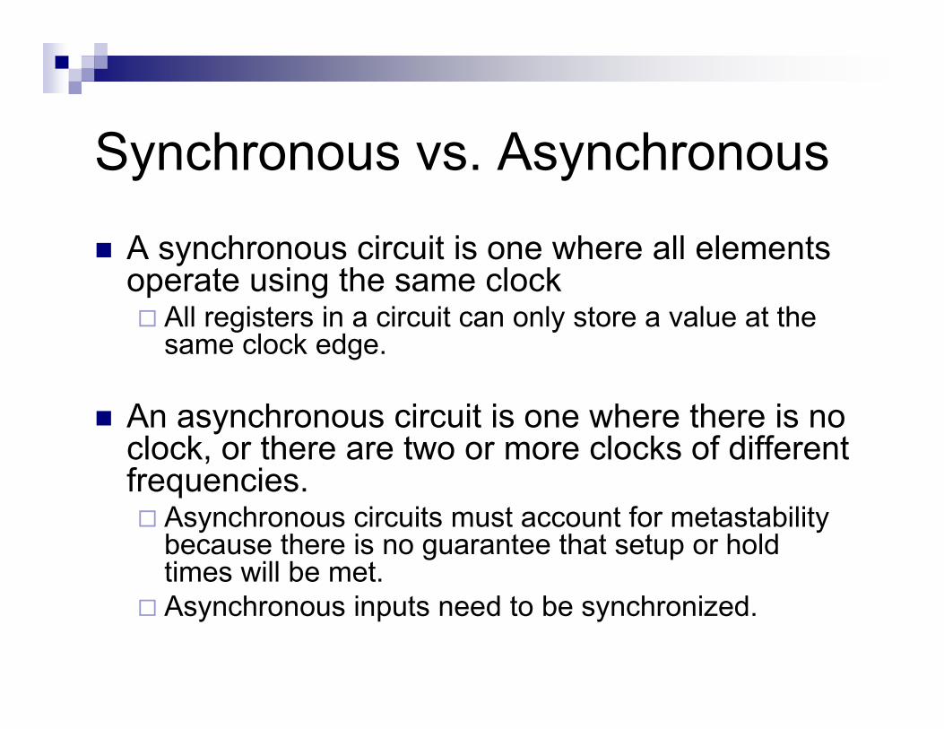
Synchronous vs. Asynchronous
� A synchronous circuit is one where all elements operate using the same clock� All registers in a circuit can only store a value at the
same clock edge.
� An asynchronous circuit is one where there is no clock, or there are two or more clocks of different frequencies.� Asynchronous circuits must account for metastability
because there is no guarantee that setup or hold times will be met.
� Asynchronous inputs need to be synchronized.
Impediments to Synchronous
Design
� Clock Skew
� The difference between the arrival times of a clock edge at different devices/gates
� Subtracts from the hold-time margin� Hold-time margin = tffpd(min) + tcomb(min) – thold – tskew(max)
� Can be caused by� Long paths
� Gated clocks
� Clock skew can cause incorrect values to be sampled, or even metastability!
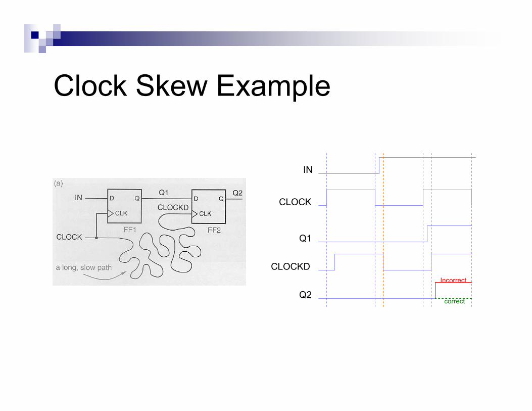
Clock Skew Example
IN
CLOCKD
CLOCK
Incorrect
correct
Q1
Q2
Impediments to Synchronous
Design
� Asynchronous Inputs
� The input is not in sync with the clock of the
synchronous circuit
� Will undoubtedly cause metastability
� The input must be synchronized.
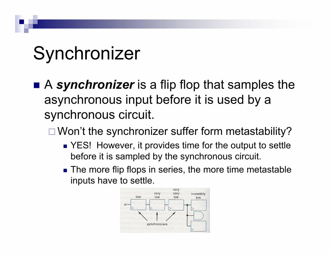
Synchronizer
� A synchronizer is a flip flop that samples the
asynchronous input before it is used by a
synchronous circuit.
�Won’t the synchronizer suffer form metastability?
� YES! However, it provides time for the output to settle
before it is sampled by the synchronous circuit.
� The more flip flops in series, the more time metastable
inputs have to settle.
Synchronizer Failure
� Failure is said to occur if a synchronizer output is
sampled when still in a metastable state.
� To avoid metastability
� Wait “long enough” before sampling the
synchronizer output.
� The output must settle within the Resolution
Time
� tr = tclk – tcomb – tsetup
� So, what is a good Resolution Time?
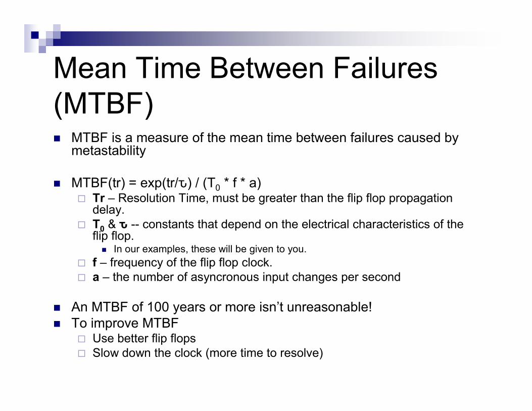
Mean Time Between Failures
(MTBF)� MTBF is a measure of the mean time between failures caused by
metastability
� MTBF(tr) = exp(tr/ԏ) / (T0 * f * a)� Tr – Resolution Time, must be greater than the flip flop propagation
delay.
� T0 & ԏ -- constants that depend on the electrical characteristics of the flip flop.
� In our examples, these will be given to you.
� f – frequency of the flip flop clock.
� a – the number of asyncronous input changes per second
� An MTBF of 100 years or more isn’t unreasonable!
� To improve MTBF� Use better flip flops
� Slow down the clock (more time to resolve)
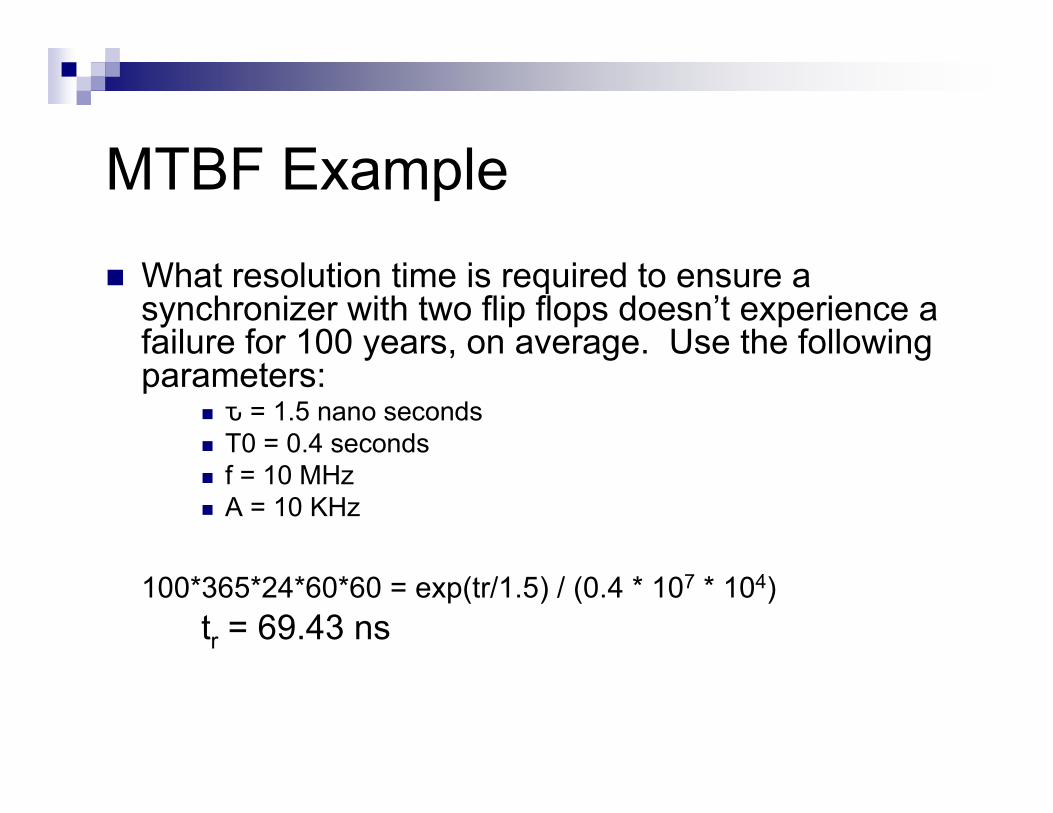
MTBF Example
� What resolution time is required to ensure a synchronizer with two flip flops doesn’t experience a failure for 100 years, on average. Use the following parameters:
� ԏ = 1.5 nano seconds
� T0 = 0.4 seconds
� f = 10 MHz
� A = 10 KHz
100*365*24*60*60 = exp(tr/1.5) / (0.4 * 107 * 104)
tr = 69.43 ns
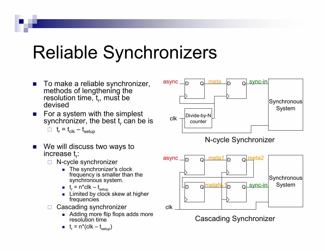
Reliable Synchronizers
� To make a reliable synchronizer, methods of lengthening the resolution time, tr, must be devised
� For a system with the simplest synchronizer, the best tr can be is � tr = tclk – tsetup
� We will discuss two ways to increase tr:� N-cycle synchronizer
� The synchronizer’s clock frequency is smaller than the synchronous system.
� tr = n*clk – tsetup
� Limited by clock skew at higher frequencies
� Cascading synchronizer� Adding more flip flops adds more
resolution time
� tr = n*(clk – tsetup)
D Q D Q
Divide-by-N
counter
Synchronous
System
meta sync-inasync
clk
N-cycle Synchronizer
D Q D Q
Synchronous
System
meta1async
clk
Cascading Synchronizer
D Q D QmetaN-1 sync-in
meta2