Embed Size (px)
Citation preview
Sensors & Transducers, Vol. 156, Issue 9, September 2013, pp. 1-9
1
SSSeeennnsssooorrrsss &&& TTTrrraaannnsssddduuuccceeerrrsss
© 2013 by IFSAhttp://www.sensorsportal.com
The Novel Image Signal Analysis of Monitoring Video Based on CMOS Image Sensor
1 Junhui FU, 2 Jingqiao LV
1 Henan Institute of Science and Technology, Henan Xinxiang, 453003, China 2 Xinxiang Medical University, Henan Xinxiang, 453003, China
1 Tel.: 13782582500 1 E-mail: [email protected]
Received: 1 September 2013 /Accepted: 25 August 2013 /Published: 30 September 2013 Abstract: The image sensor is the most important part of video and still image processing line in digital video or still camera. Data of CMOS process will produce noise in long transmission distance; therefore it must first be amplified and integrated each pixel data. The choice of medium and apparatus for transmitting image and the other the control signal will be directly related to the quality and reliability of the monitoring system. CMOS image sensor has the characteristics of low power, high integration and flexible function. The paper proposes the novel image signal analysis of monitoring video based on CMOS image sensor. In this paper, simulation results shows by using analog signal hardware simulation that the system can achieve the intended function and achieve the ideal effect. Copyright © 2013 IFSA. Keywords: CMOS, Image sensor, Image signal analysis.
1. Introduction
Image sensor is the principle of photoelectric conversion converts the image data into a device for a series of electronic signals. Contact image sensor CIS is a new type of image sensor appeared in the late 80’s, is a kind of photoelectric scanning device based on CMOS technology. CIS compared to CCD has the advantages of small volume, high speed, low cost, simple installation and debugging etc. But whether CIS or CCD should consider the interference signal, and it is sensor bias and other factors on the image signal, only to exclude these effects, to a true representation of image information.
CMOS image sensor is produced in the nineteen eighties, the manufacturing technology of CMOS technology was not high, and so the noise sensor in the application of large, commercial process has been very slow. Now, with the continuous improvement process, the application range of CMOS image sensor
is also expanding, relates to the digital products, communications, industrial, medical and other fields. Compared with CCD, CMOS image sensor has the advantages of small volume, low power consumption, low cost [1]. CMOS image sensor, IBIS5-B-1300 image sensor is a high performance, high dynamic range. Image sensor work needs to have driven timing signal is correct.
The system is mainly composed of a plane mirror tracking device, control and drive circuit, position limiting circuit, CMOS image sensor etc. Tracking device object, image sensor is fixed on the plane mirror center. The image sensor products are mainly divided into CCD, CMOS and CIS sensor three. At present, CMOS is not only inexpensive, and has realized the digital output, software programmable control, greatly reduce the difficulty of system design; improve the flexibility of the system, design of anti-interference and stability.
Article number P_1319
Sensors & Transducers, Vol. 156, Issue 9, September 2013, pp. 1-9
2
The image sensor is according to the manufacturing process and design. Therefore, the final device, light enters from the front line of control between the metal, and then focused on the photoelectric detector. Since, for the larger pixels, FSI is very effective, because the pixel stack (pixel stack) and the height of the pixel area ratio is large, the pixel aperture is large. Pixel shrinking to a series of pixel technology innovation is to solve the limitations of front illumination technology in material and manufacture. For example, FSI has to take a number of technical innovation and process improvement, such as the shape optimization of micro lens, color filter, optimization of concave type pixel array, light guides and antireflection coating technology, optical path optimization FSI pixels.
Recently the CMOS image sensor attached importance to the primary reason is that the past is much lower than the sensitivity of the CCD gradually resolved. As compared with CCD, CMOS sensor has a better production, and it is easy to implement other logic circuits, SoC (System on Chip) products, and it is difficult to achieve in the CCD. Especially the CMoS sensor, unlike the CCD requires special manufacturing processes; it can be directly used for DRAM and other large batch production equipment. In this way, CMOS image sensor is likely to cost structure formation is different from that of CCD image sensor. The paper proposes the novel image signal analysis of monitoring video based on CMOS image sensor.
2. Analysis Monitoring Video of Image Sensor In the monitoring system, monitoring and image
transmission is a vital part of the system, the choice of medium and apparatus for transmitting image and the other the control signal will be directly related to the quality and reliability of the monitoring system. At present, in the monitoring system for image signal transmission medium main coaxial cable, twisted pair and optical fiber, transmission equipment are corresponding to the coaxial video amplifier, twisted pair video transmission equipment and optical.
This change in the field of image sensor is a microcosm of the sensor technology changes. New technology development of new features, the biggest characteristic of sensor technology is introduced into the multidisciplinary now, along with the electronics, MEMS (Micro-Electro-Mechanical System), the rapid development of biotechnology, physics, chemistry, optics and so on technology, as well as human cognition of natural change, sensor technology has entered a critical stage from traditional to new breakthrough sensor technology development, is expected in the future will show the miniaturization, digitization, multifunction, intelligent and networked trend.
Because the camera optical axis and the ground form a certain angle, so the imaging are trapezoidal distortion; in order to expand the field of vision, the wide-angle lens is increasingly used by many teams, so there is a barrel distortion. These two kinds of distortion, each using wide-angle lens camera team have problems [2]. Many teams have avoided this problem, directly using the pixel image after preprocessing control. But if the pixel is converted into the actual physical coordinates, is undoubtedly more intuitive, convenient for programming or modeling, and the method proposed in this paper, which can solve these two kinds of distortion effectively, the actual operation is not complicated.
Image acquisition is the key part of security and surveillance video chain, it is because it is closely related with the image quality acquired for image signal processing ability to extract effective information from the video stream, may seem esoteric, but in fact, is the sensor quality and processing quality of the combination sensor output. The development trend of safety monitoring system is the image processing function of migration – to the network edge is moved to a camera inside, close to the sensor, as is shown by equation 1.
))()(())()(())(),(( kxkRkxkRkukxL T (1)
Remove the signal on CMOS imaging device in
the acquisition of photoelectric image signals at the same time, the image information it and at the same time of each unit, so the speed is much faster than the CCD imaging device. Because the CMOS imaging device, the column electrode can be high-speed driving, plus on the same chip as the A/D conversion, image signal can quickly take out, so it can move at a very high frame rates. If some designed for machine vision CMOS, claims can be up to 1000 frames per second frame.
Control for position, through the I2C bus with the external microprocessor to display controller route in FPGA. A total of 256 control and parameter register. In order to avoid the emergence of television interference, through the parameter I2C write must deal with in the blanking period. Data input and can be activated, the processor release control register. Through further register, processor controller rows currently displayed. These functions can be solved directly in FPGA design. According to the monitoring of the IC2 register set, designers need from IC2 device (slave), I/O port, state machine replication, and these parameters, the access from IC2 device (slave) internal memory interface, providing for arbitration. For VHDL or Verilog HDL to develop the FPGA spend relatively more time, code reusability is limited to HDL coding controller.
Because the experimental plane and true sight plane is a pure geometric relation, so this part of the conversion function can use geometric derivation. The formula is more complex, not the one listed here. The disadvantage is that a lot of formula of the
Sensors & Transducers, Vol. 156, Issue 9, September 2013, pp. 1-9
3
maximum of sin(), cos(), the operation of trigonometric function, but the single-chip to do this operation will spend a lot of time, so we should try to avoid trigonometric, square root operation. Moreover, if the wide-angle lens or camera frame lower, B will be from the A point far away and cannot find B. So this method is not universal. The experiment itself is more complex, as is shown by equation 2.
1
1
2,
2 ~1)(ˆ
N
Lkkj
jjX
j
WM
v (2)
Using these sensors manufacturers interface, so that the electronic image signal from the sensor, and into the processing logic downstream. FPGA provides a cost effective, very small size of the programmable logic platform, can easily converts the signal from the image sensor of the interface to a digital signal, the logic for downstream processing.
FPGA provides programmable mechanism of cost-effective, to adapt to a variety of signal coding scheme, register management schemes and sensor interfaces, and different types of sensors to provide programming support.
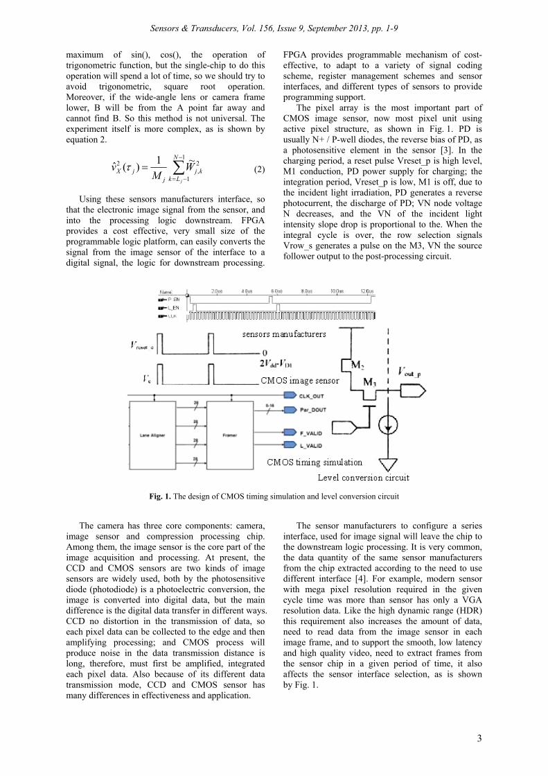
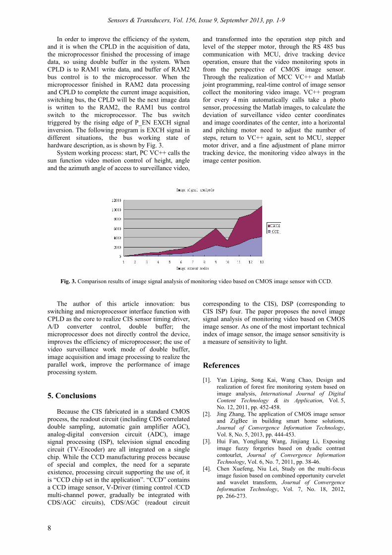
The pixel array is the most important part of CMOS image sensor, now most pixel unit using active pixel structure, as shown in Fig. 1. PD is usually N+ / P-well diodes, the reverse bias of PD, as a photosensitive element in the sensor [3]. In the charging period, a reset pulse Vreset_p is high level, M1 conduction, PD power supply for charging; the integration period, Vreset_p is low, M1 is off, due to the incident light irradiation, PD generates a reverse photocurrent, the discharge of PD; VN node voltage N decreases, and the VN of the incident light intensity slope drop is proportional to the. When the integral cycle is over, the row selection signals Vrow_s generates a pulse on the M3, VN the source follower output to the post-processing circuit.
Fig. 1. The design of CMOS timing simulation and level conversion circuit
The camera has three core components: camera, image sensor and compression processing chip. Among them, the image sensor is the core part of the image acquisition and processing. At present, the CCD and CMOS sensors are two kinds of image sensors are widely used, both by the photosensitive diode (photodiode) is a photoelectric conversion, the image is converted into digital data, but the main difference is the digital data transfer in different ways. CCD no distortion in the transmission of data, so each pixel data can be collected to the edge and then amplifying processing; and CMOS process will produce noise in the data transmission distance is long, therefore, must first be amplified, integrated each pixel data. Also because of its different data transmission mode, CCD and CMOS sensor has many differences in effectiveness and application.
The sensor manufacturers to configure a series interface, used for image signal will leave the chip to the downstream logic processing. It is very common, the data quantity of the same sensor manufacturers from the chip extracted according to the need to use different interface [4]. For example, modern sensor with mega pixel resolution required in the given cycle time was more than sensor has only a VGA resolution data. Like the high dynamic range (HDR) this requirement also increases the amount of data, need to read data from the image sensor in each image frame, and to support the smooth, low latency and high quality video, need to extract frames from the sensor chip in a given period of time, it also affects the sensor interface selection, as is shown by Fig. 1.
Sensors & Transducers, Vol. 156, Issue 9, September 2013, pp. 1-9
4
In addition to mobile phone market, OV7675 has attracted a notebook computer, Net book and Webcam customers pay more attention to. The OV7675's small size allowed ultra-thin camera module, when combined with the low light performance is remarkable, which of these terminal market becomes an attractive solution. 1/9 inch OV7675 using 2.5 micron OmniPixel3 – a unique HS ™ pixel design, which makes it possible to provide first-class low light sensitivity best (1800 MV/Lux seconds), relative to the solution of most competitive VGA, greatly reduce the noise and provides excellent color reproduction. The OV7675 SOC sensor provides full functional integrity of the VGA (640x480) camera, is able to run at full resolution at a rate of 30 frames per second, and the user can fully control the image quality, format and output data transmission.
Most of the ISP (image processing) parallel sensor interface device supports the traditional CMOS, but usually lack of high-speed serial interface support. Many ISP parallel running speed interface is far more than the parallel interface sensor. However, because the sensor is moved to different serial interface, ISP logic device needs to switch to the parallel interface. Therefore FPGA bridging devices require high speed serial data into parallel format. For manufacturers of ASSP signal processing (they have the support of parallel CMOS sensor interface faster ready-made products), FPGA solves is connected to a high speed serial sensor problem.
Because the CMOS sensor using CMOS technology semiconductor circuit is the most commonly used, can easily be peripheral circuit (such as AGC, CDS, Timing, generator, or DSP) is integrated into the sensor chip, so it can save the periphery chip cost; in addition, because CCD uses charge transfer way of transmitting data, as long as there is a pixel cannot run, will lead to a whole row of data cannot be transmitted, so CCD control sensors yield many more than the CMOS sensor is difficult, even experienced manufacturer also is very difficult in the products of the half a year to break through the 50 % level, therefore, the cost will be higher than the CCD sensor, CMOS sensor, as is shown by equation 3.
),(,),(1
)( 2112
2
1
xxxyxIyy
xPVy
yy
(3)
The FPGA chip is parallel operation, each oscillation cycle can perform tasks, while the microcontroller (such as the 8051 series) of each instruction requires 12 oscillation cycles. For example, changes in I/O port of the fastest also need 24 oscillation cycle, while FPGA only need 2 oscillation cycle, so the oscillation period under the same, FPGA faster [5].
From the current trend, CMOS wins a significantly greater chance. On the one hand, with the development of technology, the sensitivity of
CMOS is improved rapidly, it is reported on the market at present is committed to research CMOS makers have developed CMOS specific 720 p and 1080 p device sensitivity performance with CCD approach. On the other hand, although the same size CCD sensor resolution is better than CMOS sensor, but if we do not consider the size limit, the advantage of CMOS in the volume rate can effectively overcome the difficulties of large size of photosensitive component manufacture, so CMOS will have more advantage in higher resolution. In addition, the response speeds of the CMOS faster than CCD, a large amount of data, so it is more suitable to the characteristics of high- definition monitor.
Programmable logic as a bridge between the image sensor and ASSP is facing three challenges. First of all, the FPGA must provide support for the interface signal. Second, FPGA I/O must have the gearing logical enough to support a fast serial sensor interface. Third, the FPGA must provide cost-effective very small size, to adapt to the modern camera for compact appearance requirements.
Color sensor used in this design is CLS9032. The sensor has 2 vertical connecting the PN junction, the thickness can be to an optical filter to the role of color sensors play. The shorter wavelengths of light on the silicon surface are absorbed, and the longer wavelength light to reach the deeper position will be absorbed. This sensitivity based on spectrum, to select the signal according to the wavelength of light (color). The use of logarithmic current between the 2 photodiode ratio methods is as signal processing. Irradiation with light of different colors, the 3 pin of the color red, green, blue sensor area will output current signal, but the current signal corresponding color pin output than the other pin output current signal strength. Using this principle can effectively avoid the output current external environment caused by the ups and downs, so this device has high reliability.
The sensor core (Sensor Core) part comprises a photosensitive array, exposure control and readout circuit, variable gain amplifier (PGA) and an analog-to-digital converter (ADC), mainly to complete the image acquisition function. Data of the original image sensor nuclear export to image processor (ISP), ISP completed a series of image processing and image conversion function, which comprises the following process: compensation, digital gain and white balance, lens shading correction, bad pixel detection and correction, color interpolation, smoothing and edge enhancement, GAMMA correction, color correction, brightness, saturation and contrast adjustment, image size conversion, color space conversion, image data packing output. The control module to complete the automatic exposure control, automatic white balance, 50 Hz/60 Hz scintillation detection and other functions, to control the sensor core and ISP, communication and multimedia processor.
Sensors & Transducers, Vol. 156, Issue 9, September 2013, pp. 1-9
5
1
0
]sin)cos([),(N
n
Rjn
nneAF
(4)
In the monitoring system, monitoring and image
transmission is a vital part of the system, the choice of medium and apparatus for transmitting image and the other the control signal will be directly related to the quality and reliability of the monitoring system. At present, in the monitoring system for image signal transmission medium main coaxial cable, twisted pair and optical fiber, transmission equipment are corresponding to the coaxial video amplifier, twisted pair video transmission equipment and optical.
In the process of use, there are moments in non detection work. But this system also is in working state, SOPC will control the A/D converter to sample and the SOPC itself will be processed after the conversion to digital signals, and produces the color alert. In order to eliminate the false alarm and it is required magnification control amplifier. The incident differs a few nm light is amplified; the electric signals of the great difference, the numerical A/D conversion will overflow or close to overflowing. Using this characteristic, set a limit value, if the value than the upper limit, then system to make non detection work of judgment, the program execution is restarted. 3. Image Signal Analysis Based
on CMOS Image Sensor
CMOS was an important chip in the computer system; it can save large amounts of data required for the system boot. In the early nineteen seventies, it was found, introducing CMOS photo diode can be used as a sensor, but in terms of resolution, noise, power consumption and image quality than CCD at the time difference, could not obtain development. With the development of CMOS technology, CMOS technology uses standard CMOS imaging device for producing high quality, low cost. This device is convenient for mass production, the characteristics of low power consumption and low cost are businessmen dream of. Now, CCD and CMOS both exist, CCD temporary or “mainstream”, but the CMOS will replace CCD and become the mainstream of the image sensor.
According to the control timing characteristics of CIS sensor, CPLD sensor provides the clock signal for CIS CIS_CLK, a strobe signal CIS_SI and a light source control signal CIS_LED. When the microprocessor P_EN is set to a high level, and it is CPLD at the initial state. When P_EN is low, CPLD is in the preparation stage. At this time, once the microprocessor to L_EN tube generates a pulse signal on the foot, CPLD will then automatically generates the CIS_SI signal to start the CIS, while the internal counter CPLD to the external CLK to count. In the control signal is generated by AD converter based on
CPLD value. The timing circuit hardware description is as follows, where CNT is a 0 to 685 of the counter, as is shown by equation 5.
)()()1()1(0
iQuiuiQxixJ T
i
T
(5)
In an infrared image transmission system, multi-channel communication situation exists, the infrared image and other information through the air channels to the accused platform, send to the battlefield state * estimation, target selection and control instructions. In the wireless channel wartime always exist in the noise, interference, multipart fading and other effects, which requires the design of transmission system should adopt effective data to reduce the transmission bit rate compression method, try to save the transmission channel bandwidth, but also introduce error control mode to resist interference channel noise.
Standard IC fabrication technology and imaging technology in continuous progress, and it is promoted by the front illumination (FSI) development of image sensor technology [6]. In this technique, such as the human eye eagle, light falls in front of IC, and then through the reading circuit and interconnection, was finally converged to the photoelectric detector. FSI is the mainstream technology currently used by the image sensor, has confirmed the mass production capacity, high reliability and high yield and attractive price and other advantages, greatly promoting its application in many fields of mobile phone, notebook computer, digital camera and digital camera etc. These advantages, coupled with the high performance characteristics, making this technology has a unique cost, performance and value orientation, the future application can be further expanded.
Contact image sensor (CIS) is composed of a row of the same width and scans the original photoelectric sensor array, LED light source array and cylindrical lens array of components such as a new image sensor. These components are integrated in a strip in the square box, without the need of additional optical accessories, not to adjust the optical path and depth of field, has the advantages of simple structure, small volume, convenient application and etc. In some applications of CIS sensors than CCD or COMS sensor has incomparable advantages. In a very wide range of fax machines, scanners, currency sorter against the application of zero field, as is shown by equation 6.
2log
2))(ˆlog()( 2 jj
jXj vY
(6)
In recent years, tube designers removed from the MCP ion barrier film to get no film light tube, while adding 1 automatic door switch power supply, the switch speed control photoelectric cathode voltage, and improved the low corona imaging technology,
Sensors & Transducers, Vol. 156, Issue 9, September 2013, pp. 1-9
6
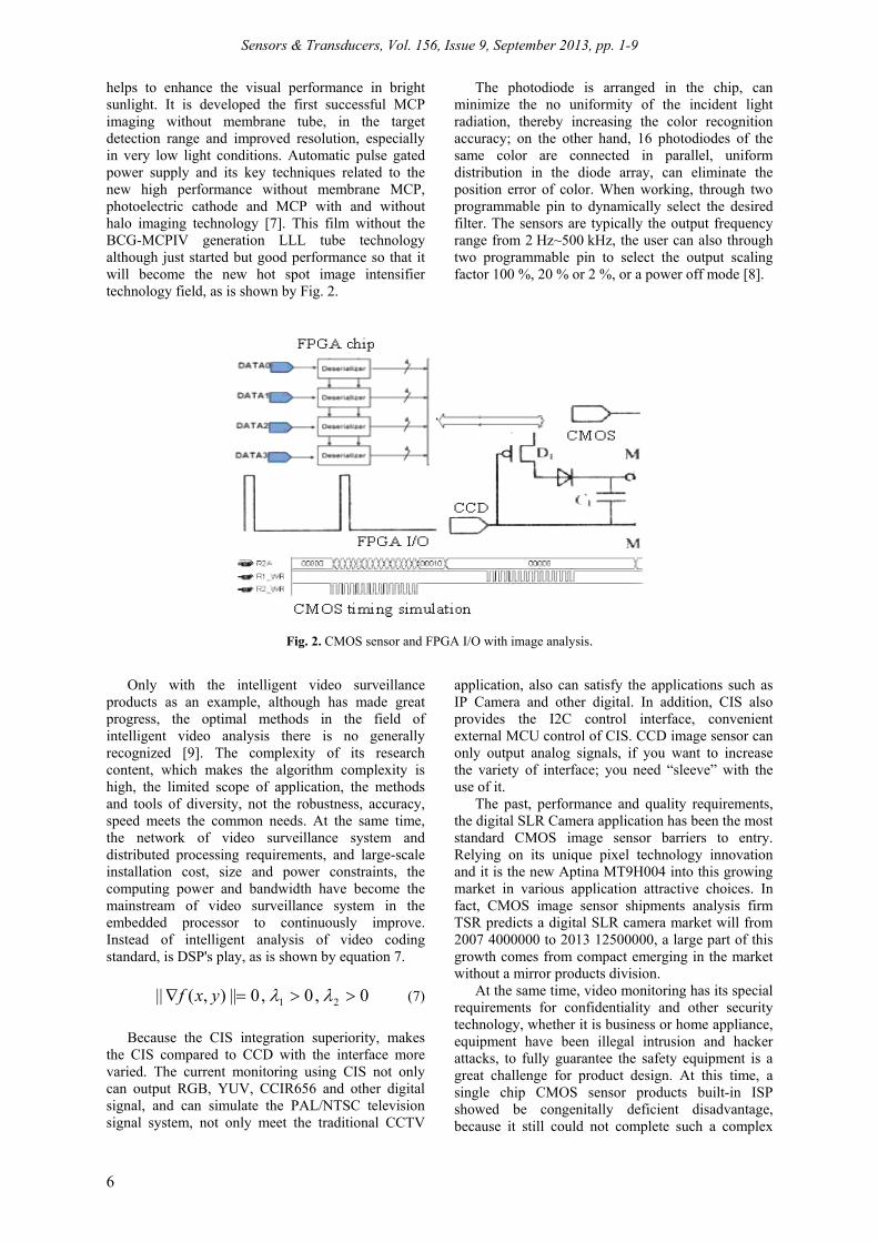
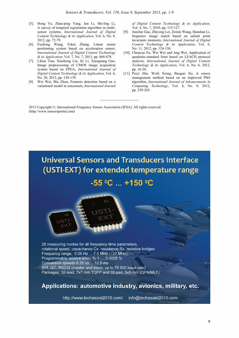
helps to enhance the visual performance in bright sunlight. It is developed the first successful MCP imaging without membrane tube, in the target detection range and improved resolution, especially in very low light conditions. Automatic pulse gated power supply and its key techniques related to the new high performance without membrane MCP, photoelectric cathode and MCP with and without halo imaging technology [7]. This film without the BCG-MCPIV generation LLL tube technology although just started but good performance so that it will become the new hot spot image intensifier technology field, as is shown by Fig. 2.
The photodiode is arranged in the chip, can minimize the no uniformity of the incident light radiation, thereby increasing the color recognition accuracy; on the other hand, 16 photodiodes of the same color are connected in parallel, uniform distribution in the diode array, can eliminate the position error of color. When working, through two programmable pin to dynamically select the desired filter. The sensors are typically the output frequency range from 2 Hz~500 kHz, the user can also through two programmable pin to select the output scaling factor 100 %, 20 % or 2 %, or a power off mode [8].
Fig. 2. CMOS sensor and FPGA I/O with image analysis.
Only with the intelligent video surveillance products as an example, although has made great progress, the optimal methods in the field of intelligent video analysis there is no generally recognized [9]. The complexity of its research content, which makes the algorithm complexity is high, the limited scope of application, the methods and tools of diversity, not the robustness, accuracy, speed meets the common needs. At the same time, the network of video surveillance system and distributed processing requirements, and large-scale installation cost, size and power constraints, the computing power and bandwidth have become the mainstream of video surveillance system in the embedded processor to continuously improve. Instead of intelligent analysis of video coding standard, is DSP's play, as is shown by equation 7.
0,0,0||),(|| 21 yxf (7)
Because the CIS integration superiority, makes
the CIS compared to CCD with the interface more varied. The current monitoring using CIS not only can output RGB, YUV, CCIR656 and other digital signal, and can simulate the PAL/NTSC television signal system, not only meet the traditional CCTV
application, also can satisfy the applications such as IP Camera and other digital. In addition, CIS also provides the I2C control interface, convenient external MCU control of CIS. CCD image sensor can only output analog signals, if you want to increase the variety of interface; you need “sleeve” with the use of it.
The past, performance and quality requirements, the digital SLR Camera application has been the most standard CMOS image sensor barriers to entry. Relying on its unique pixel technology innovation and it is the new Aptina MT9H004 into this growing market in various application attractive choices. In fact, CMOS image sensor shipments analysis firm TSR predicts a digital SLR camera market will from 2007 4000000 to 2013 12500000, a large part of this growth comes from compact emerging in the market without a mirror products division.
At the same time, video monitoring has its special requirements for confidentiality and other security technology, whether it is business or home appliance, equipment have been illegal intrusion and hacker attacks, to fully guarantee the safety equipment is a great challenge for product design. At this time, a single chip CMOS sensor products built-in ISP showed be congenitally deficient disadvantage, because it still could not complete such a complex
Sensors & Transducers, Vol. 156, Issue 9, September 2013, pp. 1-9
7
function, and must be equipped with image processor can separate meet the requirements. Although ASIC has a cost advantage, but it has inherent defects in the improvement and upgrading of the media formats, algorithm, video surveillance market continuous improvement in audio and video standard unceasing evolution and the algorithm, ASIC is inferior to many.
4. Novel Image Signal Analysis of Monitoring Video based on CMOS Image Sensor Dynamic range is a measure of the scene image
sensor for a larger difference between the performance of light and shade of light. In practical application, reflected in the image sensor can be in one image can clearly show the dark scene, and can clearly display the well-lit scene [10]. Especially when the Camera alignment window, you can see the window scene, but also can see out of the window of the scene, but not “overexposed” phenomenon. The dynamic range is higher, and that in different situations, image sensor performance. At present, the high-end CIS can achieve up to the dynamic range of more than 100 dB, and the dynamic range of common basic CCD at about 60 dB. From the dynamic scope, CIS be a stroke above.
ME1010 is a comprehensive image sensors use convenient, use the patent structure development, designed to make it easier to form a whole and computer products. CCD image sensor is different from the traditional or some new CMOS image sensor, ME1010 image sensor can provide very low X-Y address image output, so as to connect computer or DSP. It provides 352 × 290 pixels (352 × 288 effective pixels), an on-chip amplifier and supporting the ADC circuit, as is shown by equation 8.
inkii
M
Nii
N
i
nkii
kn eeuR 11
)0()(
(8)
Image signal processing traditional is
accomplished through image processor. With the continuous development of CMOS technology, also appeared the image signal processing (ISP) is built into the CMOS image sensor in the single chip products, this kind of sensor products with integrated function modules inside some image processing algorithms, including auto exposure, auto white balance, and color transformation of these basic algorithms. These kind of ASIC products appear once controversial, because although the ISP built-in sensor has lower power consumption and saving the occupied area advantage, but the mobile phone applications, from a cost perspective, ISP will be integrated in the sensor cost in mobile multimedia
processor or base band is much higher than the ISP integration.
The main difference between CMOS Image Sensor is made of a photosensitive unit and readout circuit structure is different in different manufacturing process. The photoelectric conversion realize CCD photosensitive unit, output in order to charge storage and charge transfer mode, need special process implementation; CIS image photographic unit for the photodiode, may be in general CMOS integrated circuit process to achieve, in addition to the image processing circuit, power consumption of the integrated and the lower the higher.
The image sensor can be said to be in the digital video or still camera video or still image processing line is the most important part of. If there is no sensor, there is no image signal processed [11]. As everyone knows the sensor is not standardized. In the scheme, they are different from the following: conversion of visible or infrared light into electrical signals in the way; especially before the signal from the chip, the signal by encoding and compression (sometimes) way. The sensor internal registers are programmed by the way, in order to adjust the gain, exposure time, sensor models (such as linear, HDR), the sensor image coordinates.
0)0(2)(2
QAxBuSQBBu
TTC
(9)
The CIS sensor is high speed, if directly by a
microprocessor (MPU) control timing generation CIS sensor, is the consumption of processor time and resources. Therefore, the drive circuit used CPLD as the control core; the microprocessor does not directly control the CIS sensor. The microprocessor only need is to control the CPLD page to enable signal (P_EN) and line enable signal (L_EN) the two signals line. CPLD can automatically generate A/D converter, control the timing generation, data storage and the ping-pong memory bus switching function of the CIS sequence control. The CPLD independently accomplish the image acquisition and data storage, reduced the control microprocessor on the bottom of the device, and improves the efficiency of the microprocessor in the image processing.
The main part of the software for the PC machine, and it is PC machine environment for Windows XP, using the software Microsoft Visual C++6.0 and Matlab 7. Startup VC++ is responsible for calling a sun function, altitude angle and the azimuth angle to return the current monitoring, and transformed into FYP and FWP operation steps. By calling the Windows API function, to realize the transfer of data between PC and MCU. By programming with MCC VC++ and Matlab, control of image acquisition camera in video surveillance, according to deviation monitoring the centurion coordinates and image coordinates of the center into FYP and FWP correction step number.
Sensors & Transducers, Vol. 156, Issue 9, September 2013, pp. 1-9
8
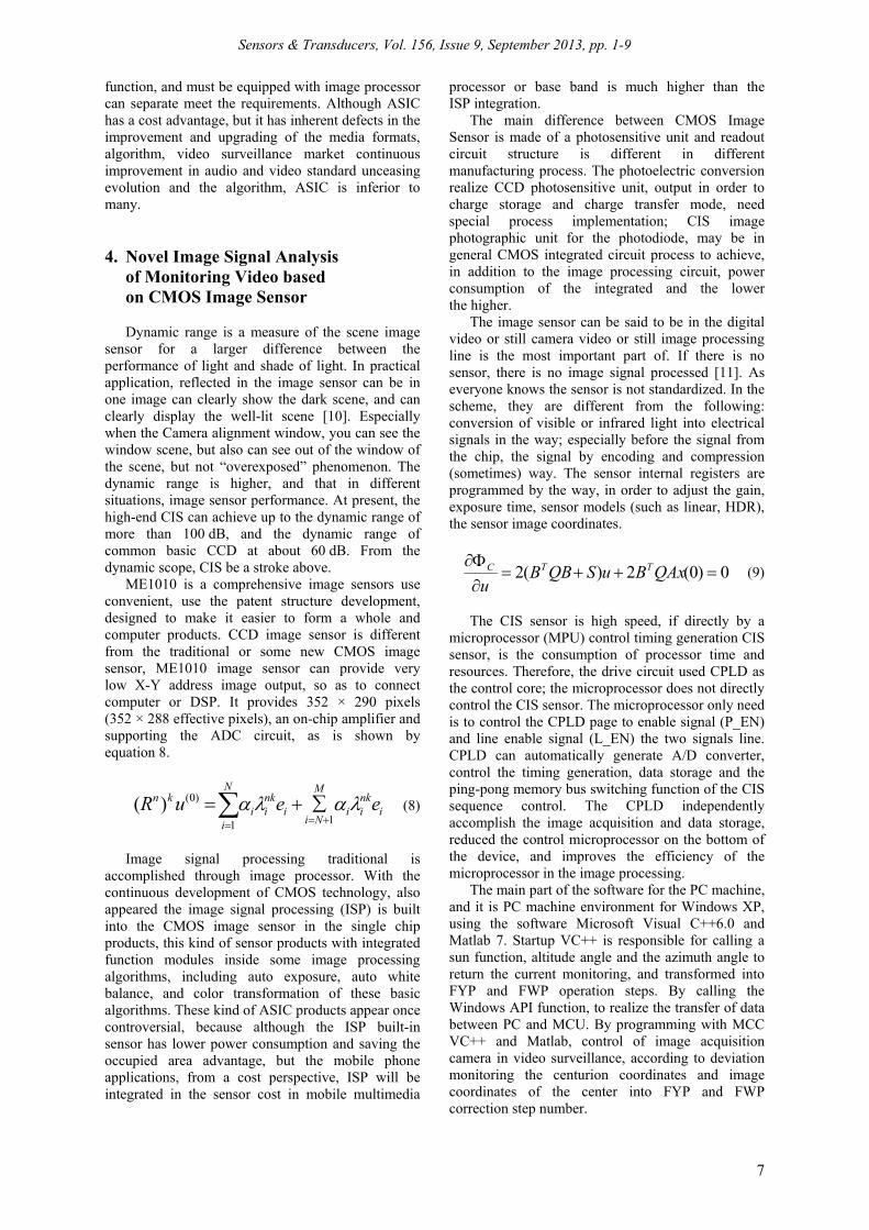
In order to improve the efficiency of the system, and it is when the CPLD in the acquisition of data, the microprocessor finished the processing of image data, so using double buffer in the system. When CPLD is to RAM1 write data, and buffer of RAM2 bus control is to the microprocessor. When the microprocessor finished in RAM2 data processing and CPLD to complete the current image acquisition, switching bus, the CPLD will be the next image data is written to the RAM2, the RAM1 bus control switch to the microprocessor. The bus switch triggered by the rising edge of P_EN EXCH signal inversion. The following program is EXCH signal in different situations, the bus working state of hardware description, as is shown by Fig. 3.
System working process: start, PC VC++ calls the sun function video motion control of height, angle and the azimuth angle of access to surveillance video,
and transformed into the operation step pitch and level of the stepper motor, through the RS 485 bus communication with MCU, drive tracking device operation, ensure that the video monitoring spots in from the perspective of CMOS image sensor. Through the realization of MCC VC++ and Matlab joint programming, real-time control of image sensor collect the monitoring video image. VC++ program for every 4 min automatically calls take a photo sensor, processing the Matlab images, to calculate the deviation of surveillance video center coordinates and image coordinates of the center, into a horizontal and pitching motor need to adjust the number of steps, return to VC++ again, sent to MCU, stepper motor driver, and a fine adjustment of plane mirror tracking device, the monitoring video always in the image center position.
Fig. 3. Comparison results of image signal analysis of monitoring video based on CMOS image sensor with CCD.
The author of this article innovation: bus switching and microprocessor interface function with CPLD as the core to realize CIS sensor timing driver, A/D converter control, double buffer; the microprocessor does not directly control the device, improves the efficiency of microprocessor; the use of video surveillance work mode of double buffer, image acquisition and image processing to realize the parallel work, improve the performance of image processing system. 5. Conclusions
Because the CIS fabricated in a standard CMOS process, the readout circuit (including CDS correlated double sampling, automatic gain amplifier AGC), analog-digital conversion circuit (ADC), image signal processing (ISP), television signal encoding circuit (TV-Encoder) are all integrated on a single chip. While the CCD manufacturing process because of special and complex, the need for a separate existence, processing circuit supporting the use of, it is “CCD chip set in the application”. “CCD” contains a CCD image sensor, V-Driver (timing control /CCD multi-channel power, gradually be integrated with CDS/AGC circuits), CDS/AGC (readout circuit
corresponding to the CIS), DSP (corresponding to CIS ISP) four. The paper proposes the novel image signal analysis of monitoring video based on CMOS image sensor. As one of the most important technical index of image sensor, the image sensor sensitivity is a measure of sensitivity to light.
References [1]. Yan Liping, Song Kai, Wang Chao, Design and
realization of forest fire monitoring system based on image analysis, International Journal of Digital Content Technology & its Application, Vol. 5, No. 12, 2011, pp. 452-458.
[2]. Jing Zhang, The application of CMOS image sensor and ZigBee in building smart home solutions, Journal of Convergence Information Technology, Vol. 8, No. 5, 2013, pp. 444-453.
[3]. Hui Fan, Yongliang Wang, Jinjiang Li, Exposing image fuzzy forgeries based on dyadic contrast contourlet, Journal of Convergence Information Technology, Vol. 6, No. 7, 2011, pp. 38-46.
[4]. Chen Xuefeng, Niu Lei, Study on the multi-focus image fusion based on combined opportunity curvelet and wavelet transform, Journal of Convergence Information Technology, Vol. 7, No. 18, 2012, pp. 266-273.
Sensors & Transducers, Vol. 156, Issue 9, September 2013, pp. 1-9
9
[5]. Hong Ye, Zhan-ping Yang, Jun Li, Shi-ling Li, A survey of temporal registration algorithm in multi-sensor systems, International Journal of Digital Content Technology & its Application, Vol. 6, No. 8, 2012, pp. 72-79.
[6]. Fuzhong Wang, Fukai Zhang, Linear motor positioning system based on acceleration sensor, International Journal of Digital Content Technology & its Application, Vol. 7, No. 7, 2013, pp. 868-878.
[7]. Likun Tian, Xiaohong Liu, Jie Li, Xiaoguang Guo, Image preprocessing of CMOS image acquisition system based on FPGA, International Journal of Digital Content Technology & its Application, Vol. 6, No. 20, 2012, pp. 130-139.
[8]. Wei Wei, Bin Zhou, Features detection based on a variational model in sensornets, International Journal
of Digital Content Technology & its Application, Vol. 4, No. 7, 2010, pp. 115-127.
[9]. Junchai Gao, Zhiyong Lei, Zemin Wang, Hanshan Li, Sequence image match based on salient point invariants moments, International Journal of Digital Content Technology & its Application, Vol. 6, No. 11, 2012, pp. 124-130.
[10]. Chunyao Fu, Wei Wei and Ang Wei, Application of quadratic-standard form based on LEACH protocol analysis, International Journal of Digital Content Technology & its Application, Vol. 6, No. 6, 2012, pp. 16-26.
[11]. Peiyi Zhu, Weili Xiong, Baoguo Xu, A sensor management method based on an improved PSO algorithm, International Journal of Advancements in Computing Technology, Vol. 4, No. 9, 2012, pp. 259-265.
___________________
2013 Copyright ©, International Frequency Sensor Association (IFSA). All rights reserved. (http://www.sensorsportal.com)


![3.5: Derivatives of Trigonometric Functions · Part 2 The Other Basic Functions ABriefReview Recall the derivatives of sin(x) and cos(x): d dx [sin(x)] = cos(x) d dx [cos(x)] = sin(x)](https://img.pdfslide.us/doc/110x75/5f4a9734fae87c301577fcbc/35-derivatives-of-trigonometric-functions-part-2-the-other-basic-functions-abriefreview.jpg)