Embed Size (px)
Citation preview

1
MCP N
anos
cale
IC D
evel
oper
s
Senio
r Des
ign E
xpo
04/27/2
012
Kenneth CorbettEndowment
2
Problem Definition
Design an optical communication Integrated Circuit (IC) chip that will allow full-duplex transmission of wireless data at a bandwidth of 100kbit/s over a distance of several meters using a Field Programmable Gate Array (FPGA) interface.

3
MCP Nano Design Team
Undergraduate Seniors pursuing a B.S.E.E.
Markus Geiger
Chris Goodale
Pin-Jen Wang

4
Consulting Faculty
Consulting Faculty
Dr. Ken Noren Dr. Suat Ay
5
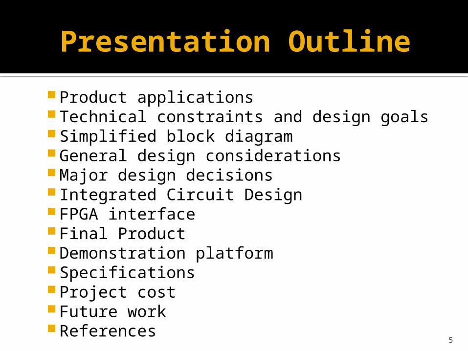
Presentation Outline
Product applications Technical constraints and design goals Simplified block diagram General design considerations Major design decisions Integrated Circuit Design FPGA interface Final Product Demonstration platform Specifications Project cost Future work References
6
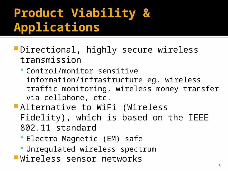
Product Viability & Applications
Directional, highly secure wireless transmission Control/monitor sensitive
information/infrastructure eg. wireless traffic monitoring, wireless money transfer via cellphone, etc.
Alternative to WiFi (Wireless Fidelity), which is based on the IEEE 802.11 standard Electro Magnetic (EM) safe Unregulated wireless spectrum
Wireless sensor networks

7
Transmitter (TX) requirements▪ Pdp_max = 500mW▪ V_bias = 1.5V (+/- 100mV)
Receiver (RX) requirements▪ Pdp_typ = 100mW▪ V_bias = -5V
Transmission distance through air▪ limited by power output of light-emitting
diode (LED) and beam half angle▪ Power decreases through air with
Technical Constraints
8
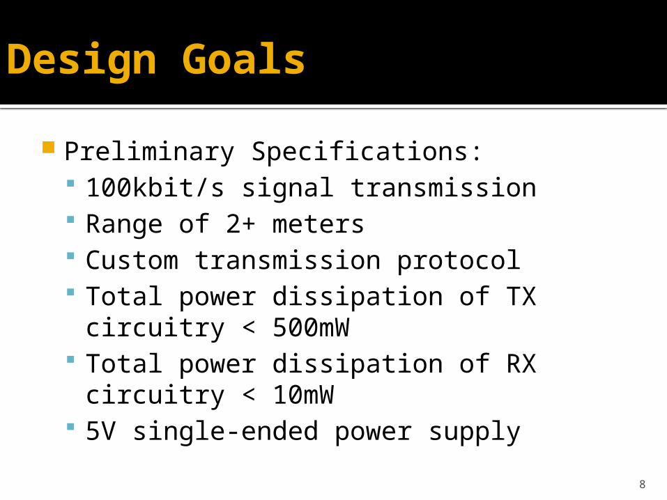
Design Goals
Preliminary Specifications: 100kbit/s signal transmission Range of 2+ meters Custom transmission protocol Total power dissipation of TX circuitry <
500mW Total power dissipation of RX circuitry <
10mW 5V single-ended power supply

9
Simplified Block Diagram
Light emitting element
(transmitter)
Photo sensitive element
(receiver)
use
r in
terf
ace
High gain trans
impedance amplifier
(TIA)
Comparator to
digitize the signal
Decoder that processes
binary input according to a communication
standard
Common Drain amplifier to provide sufficient
current
Encoder that processes the
received signal
FPGA MCPnano Transceiver IC
Free
space
Use
r
Receiver
Transmitter

10
General Design Considerations Off the shelf components
LED to transmit data (IR or visible light) Photo-diode to receive data (PIN or Avalanche)
MCPnano Integrated Circuit (IC) Design Amplifier / Comparator stages for the receiver
circuit Transmitter circuitry consisting of repeaters and
FET System integration/interface with FPGA
Connectivity/User-interface Encoding/Decoding schemes

11
Decisions: LED
INFRARED (IR) LEDVISIBLE LIGHT LED
Wavelength: 390nm to 780nm
Very susceptible to interference from ambient light (need for a versatile filter system & noise cancellation system)
May use solid-state lighting (more compact system, ease of deployment)
Wavelength: 780 nm to 950 nm
limits interference due to ambient light
Need for separate transmission circuitry
Vishay High Speed IR LED 890nm:
12
fff
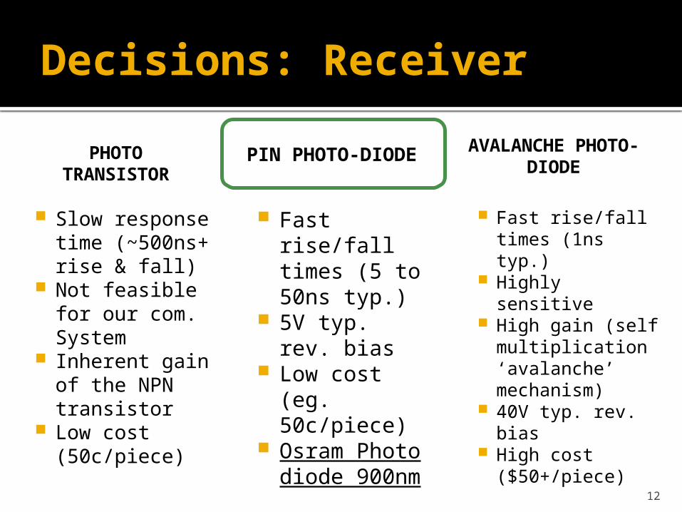
Decisions: Receiver
PHOTO TRANSISTOR
PIN PHOTO-DIODE
Slow response time (~500ns+ rise & fall)
Not feasible for our com. System
Inherent gain of the NPN transistor
Low cost (50c/piece)
AVALANCHE PHOTO-DIODE
Fast rise/fall times (5 to 50ns typ.)
5V typ. rev. bias
Low cost (eg. 50c/piece)
Osram Photo diode 900nm
Fast rise/fall times (1ns typ.)
Highly sensitive High gain (self
multiplication ‘avalanche’ mechanism)
40V typ. rev. bias
High cost ($50+/piece)
13
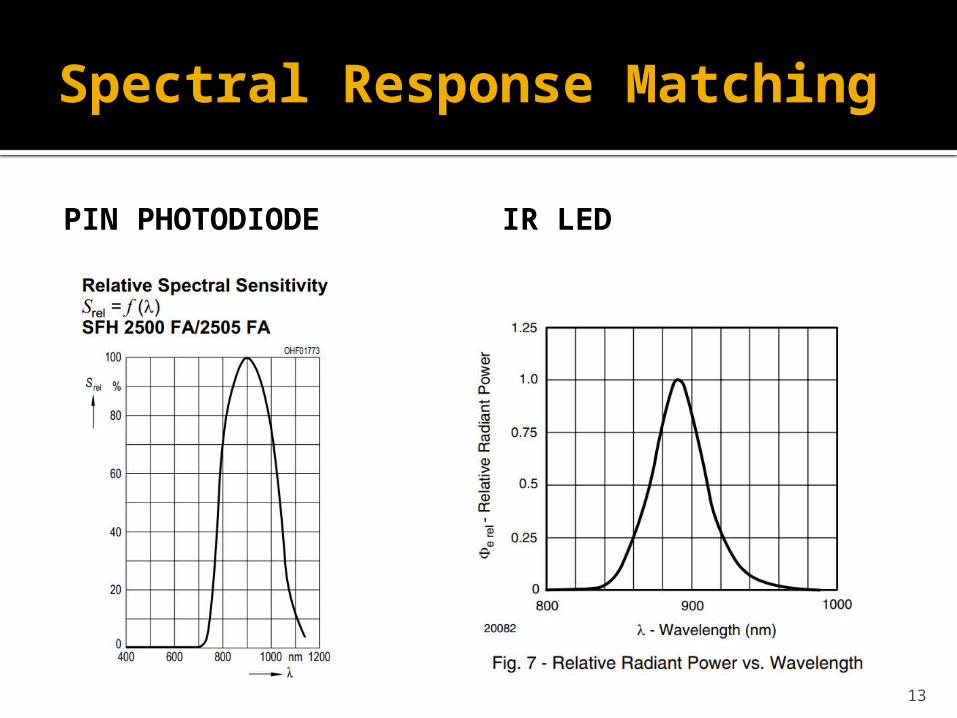
Spectral Response Matching
PIN PHOTODIODE IR LED
14
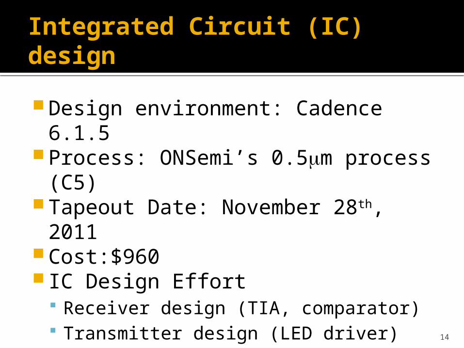
Integrated Circuit (IC) design
Design environment: Cadence 6.1.5 Process: ONSemi’s 0.5mm process
(C5) Tapeout Date: November 28th, 2011 Cost:$960 IC Design Effort
Receiver design (TIA, comparator) Transmitter design (LED driver)

15
IC Design considerations
Bias voltages to be set externally (adjustability) Allows use of different diodes Debugging
Feedback resistor/potentiometer located off chip impractical to implement 5MOhm resistor on-chip Flexibility, various distances possible
Reference current set through off-chip variable resistor (adjustable gain of opamp if needed)

16
Integrated Circuit (IC) Schematic

17
Integrated Circuit (IC) Micrograph

18
Dual Inline Package (DIP-40)
19
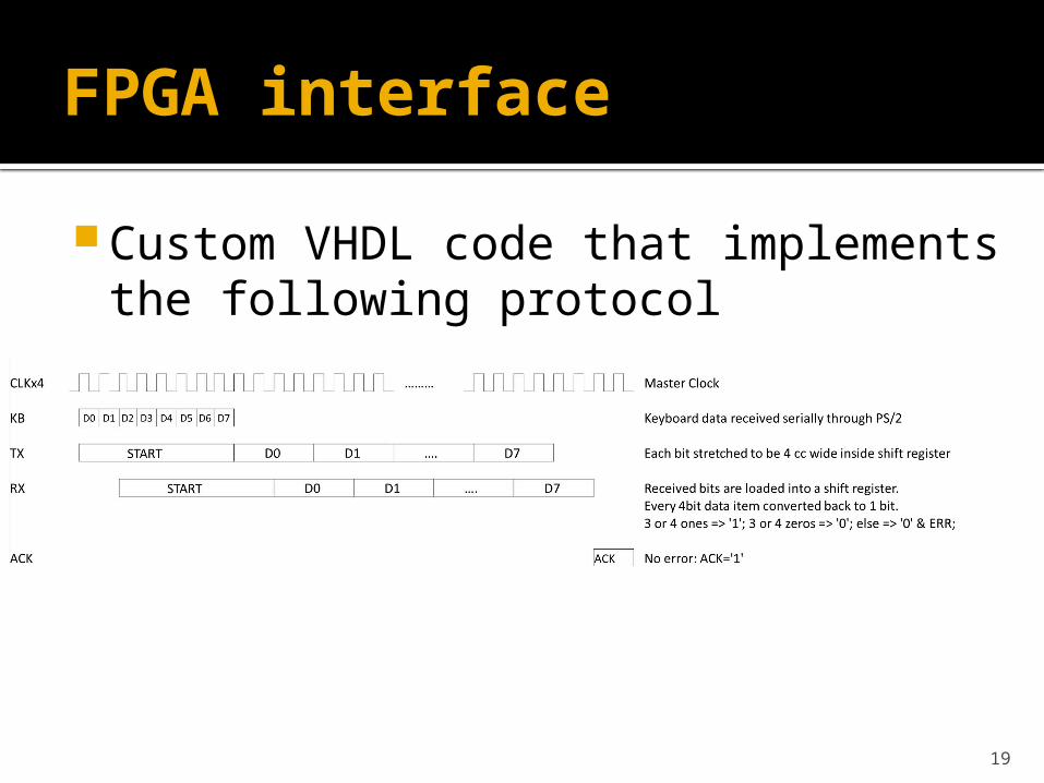
FPGA interface
Custom VHDL code that implements the following protocol

20
BASYS2 FPGA board
Special Thanks to Dr. James Frenzel (aka Dr. J) for supplying us with two Digilent BASYS2 boards
21
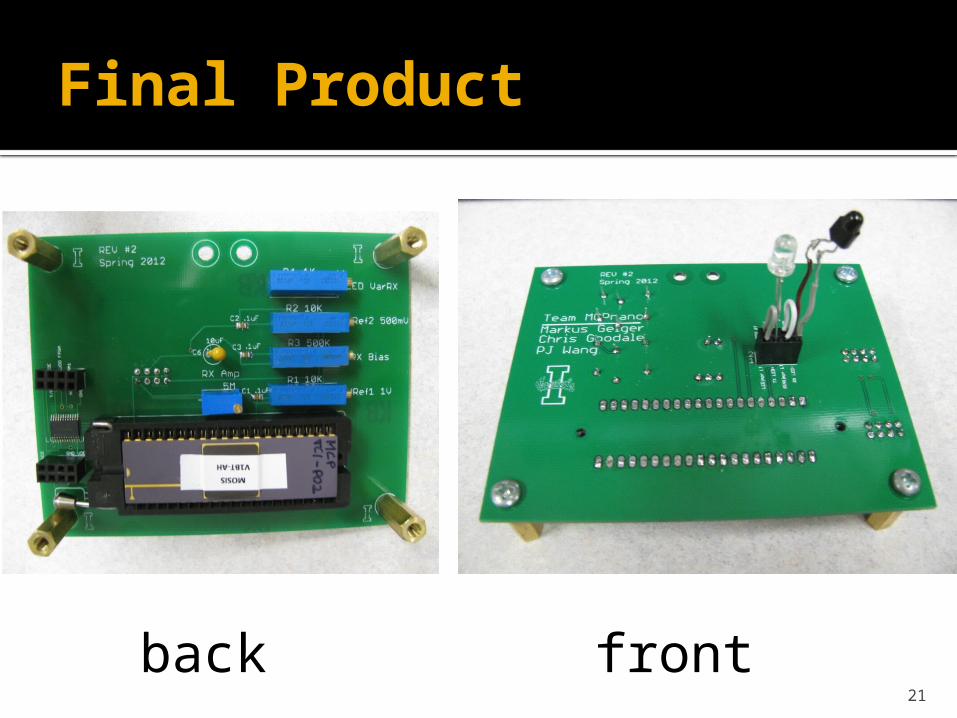
Final Product
back front
22
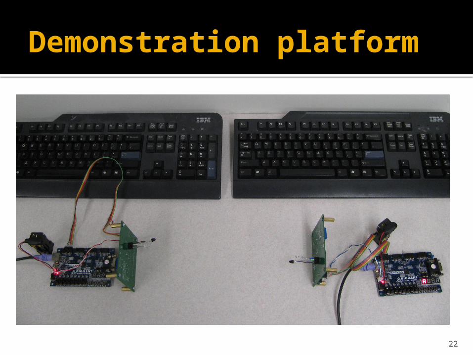
Demonstration platform

23
Transmission of letter A (“00011100”)

24
Specifications
Specifications: 100kbit/s signal transmission Maximum range of 3 meters Custom transmission protocol (FPGA in
VHDL) Total power dissipation of TX < 500mW Total power dissipation of RX < 10mW 5V single-ended power supply (battery
pack)

25
Project Deliverables
Compact IC transceiver unit on a PCB Datasheet/Documentation of
transceiver TX: LED RX: Photo-diode IC: TIA, Comparator, LED driver Discrete level shifter Custom Communication Protocol (VHDL)

26
Budget Breakdown
Parts $ 180.00
Fabrication and packaging – 20 parts (11/28/11) $ 960.00
Poster for presentation $ 100.00
Total cost $ 1,240.00

27
Future work
Incorporate the transmission protocol (using shift registers, etc.) onto the Integrated Circuit VHDL description may be used to create
the layout using automated place & route tools
Improve the comparator design on the IC (accomplish hysteresis)
Design for higher speed transmission (500kbit/s +)

28
Reference Information
FSO applications / outlook into the future http://
www.bu.edu/smartlighting/files/pdf/May808_slides_Little_FSO_Commun1.pdf
IR vs. RF https://www.audiolinks.com/articles/rfvsir/
Vishay High Speed IR LED 890nm: http
://www.mouser.com/Search/ProductDetail.aspx?qs=%2fjqivxn91cfAnyW9i5Zlpg%3d%3d
Osram Photo diode 900nm: http
://www.mouser.com/ProductDetail/Osram-Opto-Semiconductor/SFH-2500-FA-Z/?qs=K5ta8V%252bWhtarQtPwL45qKw%3d%3d