Embed Size (px)
Citation preview

Berlin 01-12-2017 Dr. J. J. Velasco-Vélez 1
Semiconductors in presence of gases: The relationship between
charge transfer and charge transport
FHI Seminar
Dr. Juan J. Velasco-VélezBerlin 01-12-2017

Berlin 01-12-2017 Dr. J. J. Velasco-Vélez 2
Outline
■ Motivation
■ Classic semicondutor theory Ideal „Bulk“
■ Semiconductor theory at the bulk edge Semiconductor surface-gas interactions
■ One example of device operation Electro-adsorptive effect Thin film transistor Drift of vacancies (dopants)
■ Remarks

Berlin 01-12-2017 Dr. J. J. Velasco-Vélez 3
Outline
■ Motivation
■ Classic semicondutor theory Ideal „Bulk“
■ Semiconductor theory at the bulk edge Semiconductor surface-gas interactions
■ One example of device operation Electro-adsorptive effect Thin film transistor Drift of vacancies (dopants)
■ Remarks

Berlin 01-12-2017 Dr. J. J. Velasco-Vélez 4
400° C
■ Change in the electron transport in semiconductors in presence of gases (Thin films) Resistance is a macro effect, however it is affected by atomic scale
interactions The interaction at the solid-gas interface influences the bulk
properties. Is the other way around also true?
Motivation

Berlin 01-12-2017 Dr. J. J. Velasco-Vélez 5
Catalysis on semiconductors
■ Why are important the semicondutors in catalysis? In most case, metals are enclosed in a semiconductor coat. Reactions take place at the surface, on the semiconductor.
■ The electron Theory of Catalysis on Semiconductors*. Heterogeneus catalytic process are based on electronic mechanisms. Elucidate the relationship between catalytic process and electronic
properties of semiconductors.
■ Theory limits Fully applicable to dielectrics. Cannot be applied directly to metals.
Based on the “many-electron“ aproach.
*F. F. Wolkenstein, W. B. Sandomirski, Dokl. Acad. Nauk. SSSR, 118, pp. 980-982, 1958.

Berlin 01-12-2017 Dr. J. J. Velasco-Vélez 6
Outline
■ Motivation
■ Classic semicondutor theory Ideal „Bulk“
■ Semiconductor theory at the bulk edge Semiconductor surface-gas interactions
■ One example of device operation Electro-adsorptive effect Thin film transistor Drift of vacancies (dopants)
■ Remarks

Berlin 01-12-2017 Dr. J. J. Velasco-Vélez 7
Semiconductors■ Is a material with an electrical conductivity between
metal and insulator Conductivity can be modified by different parameters:
TemperatureElectric field
Two types of carriers: electrons and holes

Berlin 01-12-2017 Dr. J. J. Velasco-Vélez 8
Physics of solids■ Weakly bound valence electrons interact with positively
charged atomic cores Schödinger equations rules the motion of electrons in solids
Charge doesn't change with time
Equipotential U(r)=0
solution Ψ(0)=Ψ(L)=0
Then we obtain as Eigenvalue:

Berlin 01-12-2017 Dr. J. J. Velasco-Vélez 9
Fermi distribution (U(r)=0)■ For N valence electrons, highest occupied level energy
Fermi energy
■ KE of electrons increases with temperature: distribution function

Berlin 01-12-2017 Dr. J. J. Velasco-Vélez 10
Types of semiconductors
■ Intrinsic■ Extrinsic
Type n Type p
■ Degenerate: |EC-ED|<3KBT |EV-EA|<3KBT

Berlin 01-12-2017 Dr. J. J. Velasco-Vélez 11
Conductivity in semiconductors■ Intrinsic carriers
■ Extrinsic carriers Electrons
Electron holes
■ Resistance: Resitivity
Conductivity
■ Current density
Thermo-ionic description!!

Berlin 01-12-2017 Dr. J. J. Velasco-Vélez 12
Met
al
Insu
lato
r
Sem
icon
.
Band bending (MOS)

Berlin 01-12-2017 Dr. J. J. Velasco-Vélez 13
Summary■ Semiconductor technology is everywhere
Scaling-down Close to the quantum limit LD/2: quantum confinement:
5n node (end of Moore law )
Defects grain domains Surface??
Thin Solid Films Volume 531, 15 March 2013, Pages 172-178
Shockley, Bardeen, Brattain 1948

Berlin 01-12-2017 Dr. J. J. Velasco-Vélez 14
Outline
■ Motivation
■ Classic semicondutor theory Ideal „Bulk“
■ Semiconductor theory at the bulk edge Semiconductor surface-gas interactions
■ One example of device operation Electro-adsorptive effect Thin film transistor Drift of vacancies (dopants)
■ Remarks

Berlin 01-12-2017 Dr. J. J. Velasco-Vélez 15
Surface physics
■ Thin film Co3O4 Charge transfer
informationMacro-scale
■ Cobalt thin film 240°C Chemical information
Atomic scale
*J. Wöllenstein, Sensors and Actuators B 93 (2003) 442–448

Berlin 01-12-2017 Dr. J. J. Velasco-Vélez 16
Charge Transfer Model: Needs Electron TransferBand BendingThermodynamics
Wolkenstein Model:Fully Quantum MechanicalEasy Access to EF, Semiconductor Device Modeling
LCAO:Quantum Chemistryd, p and s orbitals OverlapStereochemistrySome Access to EF
Links to Theory

Berlin 01-12-2017 Dr. J. J. Velasco-Vélez 17
Linear combination of atomic orbitals
Z.Fan and Jia G. Lu IEEE Trans Nanotech. 5(4),393,2006
Zhang, Nano Letters 4(10):1919-1924 2004
■ It can not describe macro effects: Different particle size Or tortuosity
Berlin 01-12-2017 Dr. J. J. Velasco-Vélez 18
Types of adsorptions
■ Heterogeneous catalysis bigins with the act of adsorption. Physisorption
Treated as dipol-dipol interaction (van der Waals interaction).“Long distance interactions“, from 3E-10m to 5E-10m.Novel-gas adsorbed on a metal.
Chemisorption:Weak or neutral.Strong or charged.
Ionsorption

Berlin 01-12-2017 Dr. J. J. Velasco-Vélez 19
Chemisorption
■ Chemisorbed particle simultaneosly both affinity: Acceptor Donor
■ Weak chemisorption (CL) Particle remains electrically neutral. Lattice electrons or holes do not
participate in the bond.
■ Strong chemisorption Particle adsorbs free electrons or holes
n-bond (acceptor bond), CeL.p-bond (donor bond), CpL.

Berlin 01-12-2017 Dr. J. J. Velasco-Vélez 20
Geistlinger theory■ If the electron at the conduction band and adatom has parallel spin, then a repulsive potential is
produced. Therefore due to Van der Waals forces, particles are localized at a minimum potential resulting in a physisorbed state. Alternatively, if they have antiparallel spin, the wave functions are overlapped, which leads to chemisorption. Because of this, Wolkenstein postulated a subdivision into two states: Neutral or "weak chemisorbed" and charged or "strong chemisorbed". They are represented as discrete states, meaning that.
Only strong chemisorbed molecules produce change in the conductivity
Geistlinger, H. (1993). Electron theory of thin-film gas sensors. Sensors and Actuators B: Chemical, 17(1), 47-60.

Berlin 01-12-2017 Dr. J. J. Velasco-Vélez 21
Fermi statistics
■ When still valid the Fermi statitics? Non-degenerated semiconductor,
EV+3kT<EF<EC-3kT.■ Fermi level
Controls the catalytics properties at the surface.
Once electronic equilibrium is stablished: Surface and bulk have the same Fermi
level.
■ Many factors control the Fermi level possition.
kTVeEEEf
kTEEVeEf
SFaaaaSF
/)(exp211;
/)(exp211
10
0
0

Berlin 01-12-2017 Dr. J. J. Velasco-Vélez 22
Wolkenstien Isotherm■ The Fermi level determines the probably of weak and strong occupancy
■ The number of chemisorbed particles and adsorption sites are related to the coverage:
■ The Langmuir isotherm is defined as
■ The Wolkenstein isotherm is expressed as

Berlin 01-12-2017 Dr. J. J. Velasco-Vélez 23
Co-Adsorption-Modell
■ They don‘t reach with each other■ Certain interaction
Adsorbates compite for the free adsorption centres
■ Problem to extend this model to catalysis Same problem with Langmuir isotherm
0
n
Surf ii
N N
0
1
j jj n
i ii
pf
p

Berlin 01-12-2017 Dr. J. J. Velasco-Vélez 24
eΔVs
Φ+ΔΦ
Band model (CTM)
Charge transfer
■ Band bending Surface potential. Work funtion change Depleted zone (SCR). Electrical neutrality
■ Electric properties Changes in the bulk conductivity

Berlin 01-12-2017 Dr. J. J. Velasco-Vélez 25
Charge transfer
■ Charge neutrality
■ Charge surface
■ Distribution function
■ Poisson equation
■ Surface potential
■ Movility thermally activated

Berlin 01-12-2017 Dr. J. J. Velasco-Vélez 26
Weisz limit
SFa VeEEfNN ,,)/( /0
Self Limitation of Strong (=charged) Chemisorption
This is the Weisz Effect
Electrochemistry knows the same Effect: Mott-Schottky
VVnmNZ
NforVV
µmcmEcmENNZ
S
SSCR
S
S
DSSCR
011.04)004.0(
004.0:!!!!!!!!!!!!!!!!!696
1181/141)/( 32
*Weisz, P. B. (1953). Effects of electronic charge transfer between adsorbate and solid on chemisorption and catalysis. The Journal of Chemical Physics, 21(9), 1531-1538.

Berlin 01-12-2017 Dr. J. J. Velasco-Vélez 27
Grain size Flat band limit
Crystallites dGrain ~ dSpace ChargeFermi statictis: Thermoionics vs tunneling
0
2r
D
D
kTLe N
Barsan, N., & Weimar, U. (2001). Conduction model of metal oxide gas sensors. Journal of Electroceramics, 7(3), 143-167.

Berlin 01-12-2017 Dr. J. J. Velasco-Vélez 28
Summary
■ Charge transport and transfer description Flat band conditions (Fermi-
Dirac statistic): Thermo-ionic
Wolkenstein isotherm Charge transfer
■ Complex description Schrödinger equation Shockley-Read statictics:
Tunneling

Berlin 01-12-2017 Dr. J. J. Velasco-Vélez 29
Outline
■ Motivation
■ Classic semicondutor theory Ideal „Bulk“
■ Semiconductor theory at the bulk edge Semiconductor surface-gas interactions
■ One example of device operation Electro-adsorptive effect Thin film transistor Drift of vacancies (dopants)
■ Remarks

Berlin 01-12-2017 Dr. J. J. Velasco-Vélez 30
SnO2
R [W]
Operation temperature approx: 300°C CMOS !
Surface:
EC
EV
EF
O-
O-
O-
O-
O-
CO-
SEMICONDUCTOR Surface
The challenge

Berlin 01-12-2017 Dr. J. J. Velasco-Vélez 31
Control adsorption/desorption
■ Temperature
■ Doping change Fermi level
■ Surface functionalization
■ External electric field
Nano Lett. 2011, 11, 751–756
0 100 200 300 400 500 6000,0
0,2
0,4
0,6
0,8 sensor response without Pd sensor response with Pd
sens
or re
spon
se R
/R0 -
1
temperature / °C

Berlin 01-12-2017 Dr. J. J. Velasco-Vélez 32
Electroadsorptive Effect
■ EAE: “Surface states
electrical modulation on the metal-oxide surface by means of an external electric field”

Berlin 01-12-2017 Dr. J. J. Velasco-Vélez 33
Field-Effect devices
JSE. Lilienfeld, "Method and apparatus for controlling electric currents",US Patent1, 745, 175, 1930.
It dind‘t work
Why…
O. Heil control of the layer conductivity by the surface states, 1935.
W. Shockley, GL. Pearson, "Modulation of Conductance of Thin Films of Semi-Conductors by Surface Charges", Phys. Rev. Vol. 74, pp. 232-233, 1948.
10% were mobile.
Surface states acts like electrical tramps.
F. Wolkenstein, 1958.
Patente de Lilienfeld (1930)
Patente de Heil (1935)
Short history: EAE

Berlin 01-12-2017 Dr. J. J. Velasco-Vélez 34
Adsorption of Methanol in Ge: Keier and Mikheeva 1964
O2 in ZnO: Hoenig and Lane, Surf. Sci 11, 1968
ZnO Film,E= 34 kV/cm
Oxygen
Short history: EAE

Berlin 01-12-2017 Dr. J. J. Velasco-Vélez 35
With micro always high electric field
SnO2 Gate Transistor: Popova and Stoyanov 1994
Consistency to the theory: Geistlinger 1994
SnO2 thin film: Hellmich and Müller 1996
SnO2 multi-electrode Sensor:
Hausner and Binder 1997
Thin film transistor gas sensor:
Jaegle and Wöllenstein 1998
Hellmich and Müller (1996)
Hausner and Binder (1997)
Short history: EAE

Berlin 01-12-2017 Dr. J. J. Velasco-Vélez 36
Thickness
■ Thickness:Must be in the
Debye Length range.
Energy levels are modulated
Reaction on the surface.
Sufficiently long to assure sensitivity.

Berlin 01-12-2017 Dr. J. J. Velasco-Vélez 37
Example at UHV: Fast transfer, EAE
*ChemPhysChem, 14(11), 2505-2510, 2013

Berlin 01-12-2017 Dr. J. J. Velasco-Vélez 38
Suspended Gate Effective control on the surface states Very difficult to realice this geometry
with standard CMOS processes.
Thin-Film-Transistor Gas Sensor Debye-Lenght:
Effective control of the Fermi-Level Technology: CMOS-Standard
processes
Multi-Gates Homogeneous surface reaction
Development
0
2r
D
D
kTLe N

Berlin 01-12-2017 Dr. J. J. Velasco-Vélez 39
Multigate concept

Berlin 01-12-2017 Dr. J. J. Velasco-Vélez 40
Technology■ SEM image „Multi-Gates“ Structure*
Source-Drain TFT Semiconductor SnO2 and insolator Si3N4 Contact Pt
■ Compact poly-crystalline** Non predominant orientation Grain size from 5 to 25 nm (Flat-band
condition)
■ Sensitiven layer 55 nm
*M. Lehmann, H. Frerichs **J. Wöllenstein
3 mm
Sensitive layer (55 nm)Multi-GatesSi3N4: 250nm

Berlin 01-12-2017 Dr. J. J. Velasco-Vélez 41
Technology
■ Gate electrode Multi-Gate-Structure, top view (Right) Gate electrode, Crossection (Left)

Berlin 01-12-2017 Dr. J. J. Velasco-Vélez 42
Material SnO2
■ Octahedron and rutile (a=b=0.47nm, c=0,32nm, O-Sn-O=77°20´)
■ Inert to the acid-base reaction■ Heat of formation ΔH=1.9E13(J/mol)■ Density at 300 K is 6,95 (g/cm^3)■ Melting point at 1630°C■ Direct band gap 3,5 eV■ Small electron effective mass m*=0,275 m0 ,
good conductivity■ Neutral oxygen vacancies (V0, they play role as
donators) form energy states at 0.035 eV and 0.140 eV
■ It is a n-type semiconductor due the existence of native donators levels
Berlin 01-12-2017 Dr. J. J. Velasco-Vélez 43
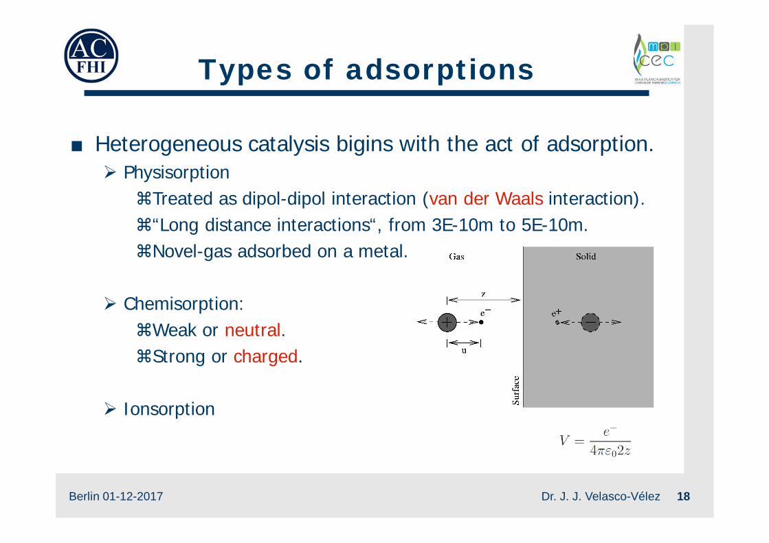
Technology■ SEM view of a multi-gate structure
Source and drain area of a multiple TFT (left) SnO2 and Si3N4, on right

Berlin 01-12-2017 Dr. J. J. Velasco-Vélez 44
Electric model ■ Sensor-Modell:
Poisson +continuity equation: Signal behaviour
Wolkenstein-Modell: Surface reaction
■ Drain-current: Controled by VDS
■ Sensor works like MOSFET with reaction to gases
( ) 0thJ e p nt
0 r
SS SCRQ Q
( )1
ppp
1
00 01 exp
ft cE Efb f
f kT

Berlin 01-12-2017 Dr. J. J. Velasco-Vélez 45
Gas measurements
■ Ideal current signal Proportional to the gate
potential Not time depending (stable)
■ Measurements with GasFET
■ Solution: Pulse at the gate
■ Parameter: Synthetic ait 80% N2 and 20%
O2, RH 40%, Work temperature 200°C, VDS=1 V

Berlin 01-12-2017 Dr. J. J. Velasco-Vélez 46
LEDs bei verschiedenen Wellenlängen (blau und UV)MesskammerGassensoren
Lichteinfluss auf gassensitive Nanoschichten
Messaufbau:
AP 2 Gasabhängige Charakterisierung der Schichten

Berlin 01-12-2017 Dr. J. J. Velasco-Vélez 47
Signal drift
*V. Brynzari et al. Sensors and Actuators B,61,143-153, 1999
■ MIS-condensator Low: C = 2.2 pf
■ Charge carriers Generation Ilumunation (LED 340 nm)
tON: 40-60 stOFF: 80-120 s
■ Surface kinetic reaction* Simulation parameters: 1010 times smaller
than real paremeters
■ Chemical reaction Vacuum measurements, same signal
behaviour

Berlin 01-12-2017 Dr. J. J. Velasco-Vélez 48
High vacuum H.L. Tuller, Massachusetts Institute of Technology*
„We're all in the same boat“

Berlin 01-12-2017 Dr. J. J. Velasco-Vélez 49
Oxygen vacancies diffusion Doping diffusion by
electric field
Fick diffusion
Fokker-Planck-Equation
Drift-Diffusions-Equation
Coupling of FP+DD by Poisson-equation
vacN D Nt
( )n e
n E n D nt
0
( )r
e n N
( ) vaceffvac
N e E N D Nt m
n(VO
+/++)
E
Vg<0EF
ECED
EV
PtSiO2
(a)
SnO2
E
EF
ECED
EV
PtSiO2
(b)
SnO2
Z
Ei
Z
n(VO+/++)
Ei
Vg<0
E
EF
ECED
EV
PtSiO2
(c)
SnO2
Z
Ei
n(VO+/++)

Berlin 01-12-2017 Dr. J. J. Velasco-Vélez 50
Drift-Diffusion simulations VG>0 V
Normalized vancies
distribution.
Internal electric field
distribution.

Berlin 01-12-2017 Dr. J. J. Velasco-Vélez 51
MemristorD.B. Strukov, Nature, Vol. 453, pp. 80-83, 2008.

Berlin 01-12-2017 Dr. J. J. Velasco-Vélez 52
Standard Halbleiter-TheorieStandard Halbleiter-Theorie
Summary
Electric Potential
Doping
EAE Adsorption
Drift
Co-Adsorption
Continuty equation
ND IDS SCR1 SCR2
Standard
Gasad.
Co-Ads.
EAE
Drift
Poisson-equation
EAE+Gas-adsorption
Gas-adsorption
Berlin 01-12-2017 Dr. J. J. Velasco-Vélez 53
Outline
■ Motivation
■ Classic semicondutor theory Ideal „Bulk“
■ Semiconductor theory at the bulk edge Semiconductor surface-gas interactions
■ One example of device operation Electro-adsorptive effect Thin film transistor Drift of vacancies (dopants)
■ Remarks

Berlin 01-12-2017 Dr. J. J. Velasco-Vélez 54
Conclusions■ Charge transport in semiconductors can be accurately described
Semiconductor theory
■ IMPORTANT: Not only the material properties are important in the charge transport also geometry!
■ Gas-solid intereaction influences the transport of charge in solid due to a charge transfer process. Atomistic intereaction at the surface modifies the conductivity of solid It can be accurately described by an extended semiconductor theory
Wolkenstein theory Charge transfer (band bending)
IMPORTANT! Check if this model is applicable directly to your system Grain size effects (Debye lenght)
■ Note: In catalytic processes the surface change continuosly: Dynamic phase transitions

Berlin 01-12-2017 Dr. J. J. Velasco-Vélez 55
Thank you!Greatings