Embed Size (px)
Citation preview

10p PhD Course 18 Lectures Nov-Dec 2011 and Jan – Feb 2012 Literature Semiconductor Physics – K. Seeger The Physics of Semiconductors – Grundmann Basic Semiconductors Physics - Hamaguchi Electronic and Optoelectronic Properties of Semiconductors - Singh Quantum Well Wires and Dots – Hartmann Wave Mechanics Applied to Semiconductor Heterostructures - Bastard Fundamentals of Semiconductor Physics and Devices – Enderlein & Horing Examination Homework Problems (6p) Written Exam (4p) Additionally Your own research area. Background courses (Solid State Physics, SC Physics, Sc Devices)
Semiconductor Physics

1. Introduction 2. Crystal and Energy Band structure 3. Semiconductor Statistics 4. Defects and Impurities 5. Optical Properties I : Absorption and Reflection 6. Optical Properties II : Recombinations 7. Carrier Diffusion 8. Scattering Processes 9. Charge Transport 10. Surface Properties 11. Low Dimensional Structures 12. Heterostructures 13. Quantum Wells/Dots 14. Organic Semiconductors 15. Graphene 16. Reserve and Summary
Course Layout

Lecture Layout Defects
• Classification • EMT Defects • Recombinations
Deep Level Defects
• SHR Kinetics • Configuration Coordinate
Electronic Structure of Deep Levels • Born-Oppenheimer Approximation • Hartree-Fock • DFA • Super Cell Calculations
Defects Examples
• Double Donor,Acceptors • Specific Defects • Semi-Insulating Semiconductors
Structural Defects

Classifications of Defects
a) Interstitial impurity atom, b) Edge dislocation, c) Self interstitial atom, d) Vacancy, e) Precipitate of impurity atoms, f) Vacancy type dislocation loop, g) Interstitial type dislocation loop, h) Substitutional impurity atom

Classifications of Defects
Intrinsic defects often causes dangling bonds, and relaxation of lattice to minimize energy.

Effective Mass Defects
In Effective-Mass Theory (EMT) the energy levels of the donor is obtained from Bohr’s theory for the hydrogen atom. The energy level for the electron in hydrogen is scaled with the ratio of the effective mass to the free electron mass and with the relative dielectric constant. For Si the EMT energy level is 6 meV, below The conduction band edge (hydrogen continuum) More detailed calculation using the Anisotropic effective mass gives 9.05 meV.

Double Donors, Acceptors
An impurity with two extra electrons give rise to a double donor. Typical examples for Si are substitutional chalcogenide atoms (VI). Similar to He atom. Donor energy for the single level Do/D+ smaller than for D+/D++. Double acceptors: Typical example substitutional Zn in Si. Zn0/Zn- Ev + 0.31 eV Zn-/Zn-- Ec – 0.55 eV

Deep Levels For deep levels the potential is short-range and the wavefunction strongly localized. Localisation in real space leads to a delocalisation in k-space. Deep levels usually traps carrier and act as recombination centers. A deep level can have different charge states depending on the occupancy of levels on the states. The energy level varies with the charge state. The energy level can also be influenced by lattice relaxation depending on charge state.

Recombination Mechanism
Excited Carriers, meaning carriers not in static thermal equilibrium, will recombine across the bandgap by different mechanisms. These can be either radiative or non-radiative.

Recombination Mechanism
For all recombination mechanisms both energy and momentum must be conserved.

Shockley-Read-Hall SRH
The theory of capture of carriers to a deep level, trap, and recombination of carriers across the bandgap is described by the SHR Kinetics.

Shockley-Read-Hall SRH
Non-degenerate semiconductor – majority of conduction band states empty – constant.

Shockley-Read-Hall SRH
Similar for holes
Recombination Rates

Shockley-Read-Hall SRH
Detailed Balance at Equilibrium, Steady-state rn = rp = 0
General assumption

Shockley-Read-Hall SRH
From statistics (Lecture 3)
Under Steady-State, rn = rp
Carrier Lifetimes

Shockley-Read-Hall SRH
Low Level Injection

Physical View of Carrier Capture
Average kinetic energy of electron in a non-defenerate
semiconductor is ½ mvth = 3/2 kT ~ 107 cm/sec at RT Capture coefficient cn and pn in units of cm3/s

Recombination Centers
Electron trap Cn >> Cp Hole trap Cn << Cp Recombination Center Cn ~ Cp

Defect Properties
Important properties of defects: Energy Level Concentration Capture Cross Section Measured by different electrical characterisation techniques.

Calculating Energylevels

Quantum Mechanics
With the solution
Where m is the electron mass, M the mass of the :th nuclei, ri the position of the i:th electron, and R and Z the position and charge of the :th nucleus. The Schrödinger equation is
For a system with N electrons and M nuclei, the full many-particle Hamiltonian is

Born-Oppenheimer Approximation
An approximation using the fact that m/M << 1. In the zero order approximation m/M=0 corresponding to M ∞ . This gives a Hamiltonian for the electrons in a static lattice.

The Adiabatic Approximation In the adiabatic approximation the contribution of the momentum operator on the electron wavefunction is neglected.
This gives a separate S.E. for the nucleii, which separates the problem into a electronical part and a vibrational part.
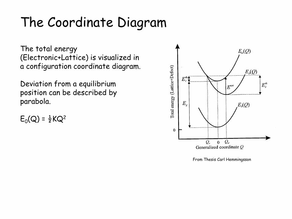
The Coordinate Diagram
The total energy (Electronic+Lattice) is visualized in a configuration coordinate diagram. Deviation from a equilibrium position can be described by parabola. E0(Q) = ½KQ2
From Thesis Carl Hemmingsson

Negative U-Centers
Some defects with strong lattice interaction has so called negative-U behaviour. This occurs when a defect, which can capture electrons, binds the second electron stronger than the first. The repulsive Coulomb force is overcome by a local distortion of the lattice lowering the total energy. Examples are vacancy in SiC, and the Z1/2 center in SiC.

Metastable Defects
From Thesis Franziska Beyer
Deep levels often have strong interaction with the lattice and generate local distortion. Different defect positions can have lowest energy depending on charge state.
Configuration B stable when occupied with electron (Bn-1). A change from configuration B A, can occur with an activation energy EA(B-A) which can come from temperature, electric fields or injection in a device. After electron emission the defect is stable in configuration A.

DX-Center
The DX is a deep level first seen in AlxGa1-xAs. It dominates the transport properties for x > 0.22. Concentration comparable to doping. The capture process is thermally activated. Optical Emission. Not identified. Proposed involving a donor and a vacancy.

EL2 Defect
EL2 is a deep donor in GaAs. Not related to impurities. Proposed to be an As antisite. Charged state has two electrons , and when charged the As atom is displaced from lattice position.

Semi-Insulating Defects Semiconductors with high resistivity, 107 – 109 cm, are called semi-insulating, SI. High resistivity is related to low free carrier concentration. SI substrates are needed for high-speed devices. SI requires fermi level in the center of the bandgap. Carriers from shallow impurities, dopands, need to be captured by deep level defects. Typical defects are transition metals: Si:Au, GaAs:Cr, InP:Fe, SiC:V In SiC also intrinsic defects such as VC
Conduction Band
Valence Band
Fermi Level

Isoelectronic Impurities
Isoelectronic impurities are usually deep levels with a short range potential. Example N on P place in GaP. The defect introduces a bound state for electron or hole. It is then charged and attracts the opposite particle via coulomb interaction.

Structural Defects

Structural Defects Structural defects often related to dangling bonds, which can cause trap levels in the bandgap. Structural defects has 1D or 2D extension.

Structural Defects
Stacking faults is one atomic plane with an error in the stacking sequence. Typical for SiC. 2D extended defect. Can occur during growth, or during operation of devices. Bipolar degredation.

Defect States Iwata et.al PRB 65, 0332 03 (2001)
Kuhr et.al JAP 92, 5863 (2002)
The change in periodicity in the crystal influences the bandstructure. In this case an extra band below the conduction band. This forms a 2D potential for electrons, similar to a quantum well. Captures electrons, which reduces number of electrons in the conduction band, which increases resistivity.

Bipolar Degredation
Electron-hole recombination gives energy to the lattice and moves dislocations. A movement of a partial dislocation in the Si-sublattice creates a stacking fault.
SWBXT Back reflection Cathodoluminescence CL
1min
2min