Embed Size (px)
Citation preview
Semiconductor Nanowire: What’s Next?Peidong Yang,* Ruoxue Yan, and Melissa Fardy
Department of Chemistry, University of California, Materials Sciences Division, Lawrence Berkeley NationalLaboratory, Berkeley, California 94720
ABSTRACT In this perspective, we take a critical look at the research progress within the nanowire community for the past decade.We discuss issues on the discovery of fundamentally new phenomena versus performance benchmarking for many of the nanowireapplications. We also notice that both the bottom-up and top-down approaches have played important roles in advancing ourfundamental understanding of this new class of nanostructures. Finally we attempt to look into the future and offer our personalopinions on what the future trends will be in nanowire research.
KEYWORDS Nanowire, photonics, energy conversion, bio-nano interface
When R. S. Wagner wrote down the followingequation Rmin ) [(2Vl)/(RT ln s)]σlv forvapor-liquid-solid whisker growth, where
Rmin is the minimum whisker radius, Vl is the molar vol-ume of the metal droplet, σlv is the liquid-vapor surfaceenergy, and s is the degree of supersaturation of the va-por,1 he probably did not expect that half a century laterresearch into semiconductor whiskers with nanoscale di-mensions would become such an active field. In the early1990s, Hitachi scientists picked up this growth techniqueand applied it to the growth of III-V nanowhiskers.2,3 Atthe time, good positional and orientational control wasachieved as well as the demonstration of the first pn junc-tions based on heterostructured nanowhiskers.4
This was followed by important studies in two separateresearch laboratories in the mid 1990s. A new whiskergrowth mechanism was proposed by William Buhro’sgroup at Washington University, where they synthesizedIII-V nanowhiskers using a solution-liquid-solid pro-cess.5 Meanwhile, the Charles Lieber group at Harvardinitiated a research program in the area of inorganicnanorods. Carbide6 and oxide nanorods7 were produced
through vapor phase conversion and transport processesin several of these early studies.
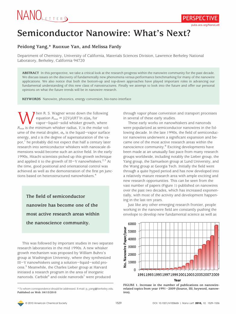
These early works on nanowhiskers and nanorodswere popularized as semiconductor nanowires in the fol-lowing decade. In the late 1990s, the field of semiconduc-tor nanowires underwent a significant expansion and be-came one of the most active research areas within thenanoscience community.8 Exciting developments havebeen made at an unusually fast pace from many researchgroups worldwide, including notably the Lieber group, theYang group, the Samuelson group at Lund University, andthe Wang group at Georgia Tech. Initially the field wentthrough a quite hyped period and has now developed intoa relatively mature research area with ample exciting andnew research opportunities. This can be seen from thevast number of papers (Figure 1) published on nanowiresover the past two decades, which has increased exponen-tially, with most of the activity and development happen-ing in the last ten years.
Just like any other emerging research frontier, peopleworking in the nanowire field are constantly pushing theenvelope to develop new fundamental science as well as
* To whom correspondence should be addressed. E-mail: [email protected] on Web: 04/15/2010
The field of semiconductor
nanowire has become one of the
most active research areas within
the nanoscience community.
FIGURE 1. Increase in the number of publications on nanowire-related topics from year 1991-2009 (Source, ISI; keyword, nanow-ires).
PERSPECTIVEpubs.acs.org/NanoLett
© 2010 American Chemical Society 1529 DOI: 10.1021/nl100665r | Nano Lett. 2010, 10, 1529–1536
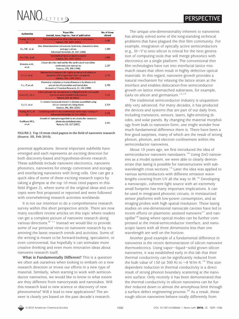
potential applications. Several important subfields haveemerged and each represents an exciting direction forboth discovery-based and hypothesis-driven research.These subfields include nanowire electronics, nanowirephotonics, nanowires for energy conversion and storage,and interfacing nanowires with living cells. One can get aquick idea of some of these exciting research topics bytaking a glimpse at the top 10 most cited papers in thisfield (Figure 2), where some of the original ideas and con-cepts were first proposed or reported and were followedwith overwhelming research activities worldwide.
It is not our intention to do a comprehensive researchsurvey within this short perspective article. There are nowmany excellent review articles on this topic where readerscan get a complete picture of nanowire research alongvarious directions.8-11 Instead we would like to providesome of our personal views on nanowire research by ex-amining the latest research trends and activities. Some ofthe writing is meant to be forward-looking, speculative, oreven controversial, but hopefully it can stimulate morecreative thinking and even more innovative ideas aboutnanowire research itself.
What is Fundamentally Different? This is a questionwe often ask ourselves when looking to embark on a newresearch direction or invest our efforts in a new type ofmaterial. Similarly, when starting to work with semicon-ductor nanowires, we would like to know to what extentare they different from nanocrystals and nanotubes. Willthis research lead to new science or discovery of newpheonomena? Will it lead to new applications? The an-swer is clearly yes based on the past decade’s research.
The unique one-dimensionality inherent to nanowireshas already solved some of the long-standing technicalproblems that have plagued the thin film community. Forexample, integration of optically active semiconductors(e.g., III-V’s) onto silicon is critical for the next genera-tion of computing tools that will merge photonics withelectronics on a single platform. The conventional thinfilm technologies have run into interfacial lattice mis-match issues that often result in highly defective opticalmaterials. In this regard, nanowire growth provides anatural mechanism for relaxing the lattice strain at theinterface and enables dislocation-free semiconductorgrowth on lattice mismatched substrates, for example,GaAs on silicon and germanium.12,13
The traditional semiconductor industry is unquestion-ably very advanced. For many decades, it has producedthe devices and systems that are part of our daily lives,including transistors, sensors, lasers, light-emitting di-odes, and solar panels. By changing the material morphol-ogy from bulk to nanowire form, one might wonder howmuch fundamental difference there is. There have been afew good surprises, many of which are the result of strongphoton, phonon, and electron confinement within thesemiconductor nanowires.
About 10 years ago, we first introduced the idea ofsemiconductor nanowire nanolasers.14 Using ZnO nanow-ires as a model system, we were able to clearly demon-strate that lasing is possible for nanostructures with sub-wavelength cross sections.15 Later the idea was applied tovarious semiconductors with different emission wave-lengths covering from UV all the way to IR.16 Developinga nanoscopic, coherent light source with an extremelysmall footprint has many important implications. It canbe used in integrated photonic circuits, in miniaturizedsensor platforms with low-power consumption, and asimaging probes with high spatial resolution. These lasingstudies on one-dimensional nanoscale cavities have led torecent efforts on plasmonic assisted nanowire17 and nan-opillar18 lasing where optical modes can be further com-pressed at the metal-semiconductor interface, and nano-scopic lasers with all three dimensions less than onewavelength are well on the horizon.
Another good example of a fundamental difference innanowires is the recent demonstration of silicon nanowirethermoelectrics. Using vapor-liquid-solid grown siliconnanowires, it was established early in this lab that theirthermal conductivity can be significantly reduced fromthe bulk value of 150 (at 300 K) to ∼8 W/m K.19 This size-dependent reduction in thermal conductivity is a directresult of strong phonon boundary scattering at the nano-wire surface. Only recently it has been demonstrated thatthe thermal conductivity in silicon nanowires can be fur-ther reduced down to almost the amorphous limit througha surface defect engineering process.20 As a result, theserough silicon nanowires behave totally differently from
FIGURE 2. Top 10 most cited papers in the field of nanowire research(Source: ISI, Feb 2010).
PERSPECTIVE
© 2010 American Chemical Society 1530 DOI: 10.1021/nl100665r | Nano Lett. 2010, 10, 1529-–1536
their bulk counterparts. At room temperature, bulk siliconis considered to be both a good thermal conductor andelectron conductor, while rough silicon nanowires are es-sentially thermal insulators and at the same time goodelectron conductors, making them good thermoelectricmaterials for waste heat recovery and power generationat a relevant temperature range.
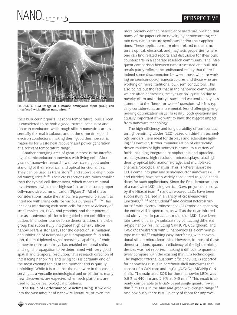
Another emerging area of great interest is the interfac-ing of semiconductor nanowires with living cells. Afteryears of nanowire research, we now have a good under-standing of their electrical and optical functionalities.They can be used as transistors21 and subwavelength opti-cal waveguides.22,23 Their cross sections are much smallerthan the typical cell dimensions, which means minimalinvasiveness, while their high surface area ensures propercell-nanowire communication (Figure 3). All of theseconsiderations make the nanowire a powerful platform tointerface with living cells for various purposes.24-26 Thisincludes interfacing with stem cells for precise delivery ofsmall molecules, DNA, and proteins, and their potentialuse as a universal platform for guided stem cell differen-tiation. In another tour de force demonstration, the Liebergroup has successfully integrated high density siliconnanowire transistor arrays for the detection, stimulation,and inhibition of neuronal signal propagation.27 In addi-tion, the multiplexed signal recording capability of entirenanowire transistor arrays has enabled temporal shiftsand signal propagation to be determined with very goodspatial and temporal resolution. This research direction ofinterfacing nanowires and living cells is certainly one ofthe most exciting topics at the moment and is quicklyunfolding. While it is true that the nanowire in this case isserving as a versatile technological tool or platform, manynew discoveries are expected when such platforms areused to tackle real biological problems.
The Issue of Performance Benchmarking. If we diveinto the vast amount of nanowire literature, or even the
more broadly defined nanoscience literature, we find thatmany of the papers claim novelty by demonstrating cer-tain new nanostructure syntheses and/or their applica-tions. These applications are often related to the struc-ture’s optical, electrical, and magnetic properties, whereone can find related reports and discussion for their bulkcounterparts in a separate research community. The infre-quent comparison between nanostructured and bulk ma-terials partly reflects the undisputed reality that there isindeed some disconnection between those who are work-ing on semiconductor nanostructures and those who areworking on more traditional bulk semiconductors. Thisalso points out the fact that in the nanowire communitywe are often addressing the “yes-or-no” question due tonovelty claim and priority issues, and we tend to pay lessattention to the “better-or-worse” question, which is typi-cally considered as an incremental, less-challenging, engi-neering optimization issue. In reality, both questions areequally important if we want to have the biggest impactfrom nanowire technology.
The high-efficiency and long-durability of semiconduc-tor light-emitting diodes (LED) based on thin-film technol-ogy renders them ideal for displays and solid-state light-ing.28 However, further miniaturization of electricallydriven multicolor light sources is crucial to a variety offields including integrated nanophotonic and optoelec-tronic systems, high-resolution microdisplays, ultrahighdensity optical information storage, and multiplexedchemical/biological analysis. This is where nanoscaleLEDs come into play and semiconductor nanowires (III-Vand nitrides) have been widely considered as good candi-dates for such applications. Since the first demonstrationof a nanowire LED using vertical GaAs pn-junction arraysby the Hitachi team,4 nanowire-based LEDs have beensuccessfully realized in a variety of cross-nanowirejunctions,29-31 longitudinal32 and coaxial heterostruc-tures33 with electroluminescence (EL) emission spanningthe entire visible spectrum, as well as the near-infraredand ultraviolet. In particular, multicolor LEDs have beenfabricated on a single substrate by contacting differentn-type nanowires, including GaN (UV), CdS (green), andCdSe (near-infrared) with Si nanowires as a common p-type material,30 enabling easy interfacing with conven-tional silicon microelectronics. However, in most of thesedemonstrations, quantum efficiency of the light-emittingdevices was not reported, making it difficult to quantita-tively compare with the existing thin film technologies.The highest external quantum efficiency (EQE) reportedfor nanowire-LEDs is in core/multishell nanowires thatconsist of n-GaN core and InxGa1-xN/GaN/p-AlGaN/p-GaNshells. The estimated EQE for these nanowire LEDs was5.8% at 440 nm and 3.9% at 540 nm.33 This result is al-ready comparable to InGaN-based single quantum-wellthin film LEDs in the blue and green wavelength range.34
And obviously there is still plenty of room for improve-
FIGURE 3. SEM image of a mouse embryonic stem (mES) cellinterfaced with silicon nanowires.24
PERSPECTIVE
© 2010 American Chemical Society 1531 DOI: 10.1021/nl100665r | Nano Lett. 2010, 10, 1529-–1536
ment by optimizing collection efficiency and interfacecontrol to minimize undesired nonradiativerecombination.
A similar comparison can be made between nanowireand conventional thin-film solar cells. Solar cells are beingpursued as environmentally friendly, renewable powersources to ease the energy crisis currently confrontinghuman society. However, it remains a challenge to makeinexpensive, high-efficiency photovoltaic devices for largescale energy conversion. Semiconductor nanowires havebeen proposed to be fundamentally advantageous forphotovoltaic applications due to their unique properties.Some of the many advantages that nanowires offer in-clude long absorption path lengths while maintainingshort distances for carrier collection/transport; interpen-etrating heterojunction interfaces, allowing efficient car-rier extraction following light absorption; strong light trap-ping in high-density nanowire arrays; and modification ofmaterial properties and cell efficiencies through size andcomposition variation of the nanostructures. Dye-sensi-tized solar cells using dense arrays of oriented, crystallineZnO nanowires as the anode have been designed to im-prove charge collection efficiency.35 The direct electricalpathways provided by the nanowires ensure the rapidcollection of carriers generated throughout the device,and an efficiency of 2.5%36 under AM 1.5 illuminationhas been demonstrated, limited primarily by the need toimprove dye-loading by increasing the surface area of thenanowire array. Coaxial silicon nanowires (p-type/intrin-sic/n-type (p-i-n)) have achieved an apparent energy con-version efficiency of up to 3.4% under AM 1.5 illumina-tion and are able to drive functional nanoelectronicsensors and logic devices.37 And more recently, stronglight-trapping effects were observed in high-density siliconcore-shell nanowire array solar cells with efficiencies upto 6%.38 Integrated with ultralow power nanosystems,such as remote and mobile chemical and environmentalsensors, nanoelectronic and nanophotonic circuitry, thesenanowire-based photovoltaic devices may serve as cleanand sustainable miniature power sources. However, itremains a scientific challenge to design and synthesizenanowires and their heterostructures with performancesexceeding that of the existing silicon photovoltaic technol-ogy, which has a commercial efficiency larger than 20%and is being pushed to it is theoretical limiting efficiencyof 29%.39 Issues to be considered include surface recom-bination problems associated with the high surface areaof the nanowires.
A couple of years ago, a nanogenerator based on ZnOnanowires40 was developed to power battery-free wirelessnanodevices by converting ambient vibrations, hydraulicenergy, or mechanical movement to electricity. Thesedevices with their varying configurations41-44 demon-strate the capability of harvesting energy from ambientvibrations in different media,41,45 even from body and
muscle movements,46 and under a variety of frequencies(<10 Hz to 41 kHz).41,42 However, the major bottleneck tothe application of these nanogenerators is their low out-put power, which is usually on the order of nanowatts(areal power density <1 µW/cm2)43,47 and low output volt-age, which is dictated by individual nanowires and is typi-cally <100 mV.44,46,48,49 In comparison, a commercialpiezo generator based on piezoceramic thin films operat-ing in the same frequency range can be 3-4 orders ofmagnitude higher in these parameters (e.g., piezoelectricheel-strike generators50). Although different strategies toimprove the output power and voltage have been pro-posed,51 these nanogenerators may never be able topower our homes or even our flash lights. However, ZnOnanowire-based nanogenerators possess unique featuresthat make them promising solutions for independent, sus-tainable, maintenance-free nanosystems that have low-power consumption, such as implantable biosensors, nan-orobotics, and possibly portable/wearable personalelectronics.
While the previous section focused on the scientificbreakthroughs achieved by constantly pushing the funda-mental limits of nanowires, here we would like to makethe case that a technological breakthrough will come onlyafter we address both “yes-or-no” and “better-or-worse”issues with all of our undivided attention. Long-term sta-bility will also be a common problem for many of thenanowire-based devices and systems. It is true for theLEDs, solar cells, and piezoelectric generators we dis-cussed here, as well as sensors, batteries, and transistors.We need to keep in mind that all of these areas have ex-isting mature industrial technologies (largely technologiesbased on thin film and bulk semiconductors). Unless thereare significant cost and/or performance benefits from us-ing nanowires, it will be difficult to displace the existingtechnologies.
Bottom-up versus Top-down. There are now manydifferent methods for making semiconductor nanowires.They are commonly placed into two categories, namely,the bottom-up and top-down approaches. The bottom-upapproach starts with individual atoms and molecules andbuilds up the desired nanostructures. For nanowire syn-thesis, this includes vapor-liquid-solid (VLS) chemicalvapor deposition, the solid-liquid-solid process, nanop-ore templating, and various hydrothermal methods. Thetop-down approach relies on dimensional reductionthrough selective etching and various nanoimprintingtechniques. Similarly, for the integration of nanowirebuilding blocks, there are also two such general ap-proaches, the first being chemical assembly such asLangmuir-Blodgett techniques, the other being litho-graphical processes. So, which one is better?
The answer as of now is a bit of both. It is clear at thispoint that we need both approaches for many of the ap-plications related to semiconductor nanowires. Synthesis-
PERSPECTIVE
© 2010 American Chemical Society 1532 DOI: 10.1021/nl100665r | Nano Lett. 2010, 10, 1529-–1536
based bottom-up approaches can be used to generatestructures with dimensions ranging from angstroms tohundreds of nanometers. On the other hand, while thefabrication based top-down processes still have difficultycreating structures below 10 nm, they have a great advan-tage when integration and addressability are concerned.
There are a couple of good examples that illustrate thevalue of both strategies. The thermoelectric performanceof silicon nanowires has been examined in both syntheticand fabricated nanowires. The Yang group has focused onVLS grown and chemically etched nanowires20 while theHeath group has had great success with their SuperlatticeNanowire Pattern Transfer (SNAP) process to producevery thin silicon nanowires.52 In both cases, similar ther-moelectric performance was observed.
The concept of nanowire based solar cells has attractedsignificant attention because of their potential benefits incarrier transport, charge separation, and light absorption.The Lieber group has developed a fairly sophiscatedcore-sheath growth and contact strategy for their siliconp-i-n nanowire solar cells with efficiencies up to 3.5%.37
On the other hand, etching and overgrowth processeshave also been developed to fabricate high density siliconcore-shell solar cells. Efficiencies up to 6% have beendemonstrated in this type of top-down fabricated nano-wire core-shell arrays.38 Here, both synthetic and fabri-cated nanowires offer similar core-shell solar cell de-signs, and therefore the same operational principle, butwith differences in interface sharpness and carrier recom-bination kinetics.
We can find a similar situation when it comes to sen-sor and laser research. On the basis of chemically synthe-sized nanowires, chemical/biological sensors53-55 andnanolasers14,56,57 have been developed in the Lieber andYang groups. On the other hand, fully integrated nano-wire chemical sensors58 and nanopillar lasers18 have beenfabricated and tested using all top-down processes. Thetop-down approach typically has the advantage of beinghigh throughput and more amenable for large scaleintegration.
As for the integration of ultrahigh density nanowirecircuitry, this has been one of the major challenges fornanowires prepared by either method. We have manydifferent methods to assemble high-density nanowire ar-rays in either two or three dimensions. However, whenone wants to carry out large scale integration, the choicesare fairly limited, especially for addressability at the singlenanowire level. In this regard, the SNAP method proposedby the Heath group is quite promising.59 They have pro-posed a demultiplexer architecture for bridging the sub-micrometer dimensions of lithographic patterning to thenanometer-scale dimensions for ultrahigh-density nano-wire circuits. This concept has been experimentally dem-onstrated on submicrometer wires and on an array of 150
silicon nanowires patterned at nanowire widths of 13 nmand a pitch of 34 nm.60
Where Is the Killer Application? So where is the killerapplication after all these years? Or is there one?
Optimistically, the field has made great progress inadvancing the fundamental science related to semicon-ductor nanowires. There are also many startups trying tocommercialize some of the important applications, includ-ing Nanosys, Alphabet Energy, Vista Therapeutics, andQuNano. Below are three areas, in our opinion, that willsee great research activity and progress in the comingyears.
Integrated Nanophotonics. Imagine what you can doif you can have a nanoscopic light source that is as smallas a semiconductor transistor.
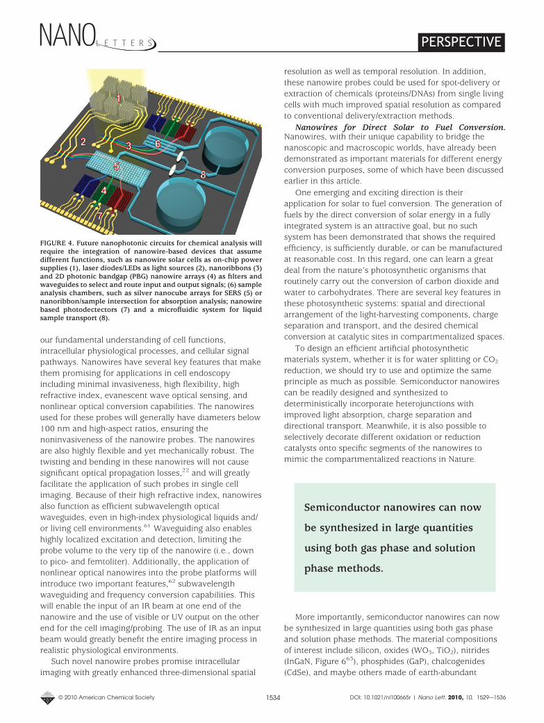
The ability to manipulate pulses of light withinsubmicrometer volumes is vital for highly integrated light-based devices, such as optical computers, to be realized.Chemically synthesized nanowires have several uniquefeatures that make them good photonic building blocks,including inherent one-dimensionality, a variety of opticaland electrical properties, good size control, low surfaceroughness and, in principle, the ability to operate bothabove and below the diffraction limit. While state-of-artlithography techniques are capable of fabricatingnanostructured features with dimensions discussed in thisarticle, chemically grown nanowires still possess uniqueadvantages such as single crystallinity, atomically smoothsurfaces and low defect density. Using a combination ofnanolithographic tools, it is highly feasible to assemblephotonic circuits (Figure 4) from a collection of nanowireelements that assume various functions, such as lightcreation, routing, and detection. Since the range ofnanowire materials now includes active, passive,nonlinear and semiconducting inorganic crystals,9
synthesizing from the bottom-up offers novel design-by-choice schemes to facilitate the assembly of multifunctioncomponents on the same substrate. Such systems can beused in parallel with existing sensing technologies such assurface-enhanced Raman spectroscopy and microfluidicsystems, and could be used in many potential areas suchas chemical/biological sensing, environmental monitoring,imaging, and information processing. Because of theirsmall footprint and low power consumption, they can beself-powered and readily embedded in cell phones orwrist-watches.
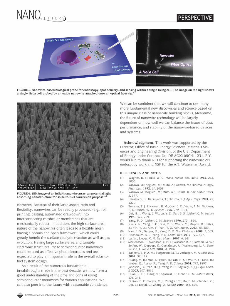
Nanowire-Based Single Cell Endoscopy. Thedevelopment of a nanoscopic coherent light source couldalso lead to a new type of nanowire probe for in situsingle cell imaging, essentially a nanowire-based singlecell endoscopy.
Development of such nanowire probes would enableus to carry out intracellular imaging and probing with highspatial resolution (Figure 5), monitor in vivo biologicalprocesses within single living cells and greatly improve
PERSPECTIVE
© 2010 American Chemical Society 1533 DOI: 10.1021/nl100665r | Nano Lett. 2010, 10, 1529-–1536
our fundamental understanding of cell functions,intracellular physiological processes, and cellular signalpathways. Nanowires have several key features that makethem promising for applications in cell endoscopyincluding minimal invasiveness, high flexibility, highrefractive index, evanescent wave optical sensing, andnonlinear optical conversion capabilities. The nanowiresused for these probes will generally have diameters below100 nm and high-aspect ratios, ensuring thenoninvasiveness of the nanowire probes. The nanowiresare also highly flexible and yet mechanically robust. Thetwisting and bending in these nanowires will not causesignificant optical propagation losses,22 and will greatlyfacilitate the application of such probes in single cellimaging. Because of their high refractive index, nanowiresalso function as efficient subwavelength opticalwaveguides, even in high-index physiological liquids and/or living cell environments.61 Waveguiding also enableshighly localized excitation and detection, limiting theprobe volume to the very tip of the nanowire (i.e., downto pico- and femtoliter). Additionally, the application ofnonlinear optical nanowires into the probe platforms willintroduce two important features,62 subwavelengthwaveguiding and frequency conversion capabilities. Thiswill enable the input of an IR beam at one end of thenanowire and the use of visible or UV output on the otherend for the cell imaging/probing. The use of IR as an inputbeam would greatly benefit the entire imaging process inrealistic physiological environments.
Such novel nanowire probes promise intracellularimaging with greatly enhanced three-dimensional spatial
resolution as well as temporal resolution. In addition,these nanowire probes could be used for spot-delivery orextraction of chemicals (proteins/DNAs) from single livingcells with much improved spatial resolution as comparedto conventional delivery/extraction methods.
Nanowires for Direct Solar to Fuel Conversion.Nanowires, with their unique capability to bridge thenanoscopic and macroscopic worlds, have already beendemonstrated as important materials for different energyconversion purposes, some of which have been discussedearlier in this article.
One emerging and exciting direction is theirapplication for solar to fuel conversion. The generation offuels by the direct conversion of solar energy in a fullyintegrated system is an attractive goal, but no suchsystem has been demonstrated that shows the requiredefficiency, is sufficiently durable, or can be manufacturedat reasonable cost. In this regard, one can learn a greatdeal from the nature’s photosynthetic organisms thatroutinely carry out the conversion of carbon dioxide andwater to carbohydrates. There are several key features inthese photosynthetic systems: spatial and directionalarrangement of the light-harvesting components, chargeseparation and transport, and the desired chemicalconversion at catalytic sites in compartmentalized spaces.
To design an efficient artificial photosyntheticmaterials system, whether it is for water splitting or CO2
reduction, we should try to use and optimize the sameprinciple as much as possible. Semiconductor nanowirescan be readily designed and synthesized todeterministically incorporate heterojunctions withimproved light absorption, charge separation anddirectional transport. Meanwhile, it is also possible toselectively decorate different oxidation or reductioncatalysts onto specific segments of the nanowires tomimic the compartmentalized reactions in Nature.
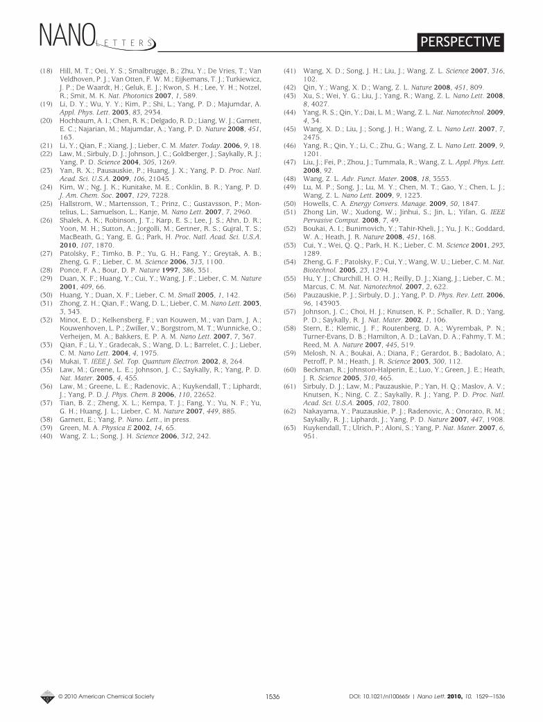
More importantly, semiconductor nanowires can nowbe synthesized in large quantities using both gas phaseand solution phase methods. The material compositionsof interest include silicon, oxides (WO3, TiO2), nitrides(InGaN, Figure 663), phosphides (GaP), chalcogenides(CdSe), and maybe others made of earth-abundant
FIGURE 4. Future nanophotonic circuits for chemical analysis willrequire the integration of nanowire-based devices that assumedifferent functions, such as nanowire solar cells as on-chip powersupplies (1), laser diodes/LEDs as light sources (2), nanoribbons (3)and 2D photonic bandgap (PBG) nanowire arrays (4) as filters andwaveguides to select and route input and output signals; (6) sampleanalysis chambers, such as silver nanocube arrays for SERS (5) ornanoribbon/sample intersection for absorption analysis; nanowirebased photodectectors (7) and a microfluidic system for liquidsample transport (8).
Semiconductor nanowires can now
be synthesized in large quantities
using both gas phase and solution
phase methods.
PERSPECTIVE
© 2010 American Chemical Society 1534 DOI: 10.1021/nl100665r | Nano Lett. 2010, 10, 1529-–1536
elements. Because of their large aspect ratio andflexibility, nanowires can be readily processed (e.g., rollprinting, casting, automated drawdown) intointerconnecting meshes or membranes that aremechanically robust. In addition, the high surface-areanature of the nanowires often leads to a flexible meshhaving a porous and open framework, which couldgreatly benefit the surface catalytic reaction as well as gasevolution. Having large surface-area and tunableelectronic structures, these semiconductor nanowirescould be used as effective photoelectrodes and areexpected to play an important role in the overall solar-to-fuel system design.
As a result of the numerous fundamentalbreakthroughs made in the past decade, we now have agood understanding of the pros and cons of usingsemiconductor nanowires for various applications. Wecan also peer into the future with reasonable confidence.
We can be confident that we will continue to see manymore fundamental new discoveries and science based onthis unique class of nanoscale building blocks. Meantime,the future of nanowire technology will be largelydependent on how well we can balance the issues of cost,performance, and stability of the nanowire-based devicesand systems.
Acknowledgment. This work was supported by theDirector, Office of Basic Energy Sciences, Materials Sci-ences and Engineering Division, of the U.S. Departmentof Energy under Contract No. DE-AC02-05CH11231. P.Y.would like to thank NIH for supporting the nanowire cellendoscopy work and NSF for the A.T. Waterman Award.
REFERENCES AND NOTES(1) Wagner, R. S.; Ellis, W. C. Trans. Metall. Soc. AIME 1965, 233,
1053.(2) Yazawa, M.; Koguchi, M.; Muto, A.; Ozawa, M.; Hiruma, K. Appl.
Phys. Lett. 1992, 61, 2051.(3) Yazawa, M.; Koguchi, M.; Muto, A.; Hiruma, K. Adv. Mater. 1993,
5, 577.(4) Haraguchi, K.; Katsuyama, T.; Hiruma, K. J. Appl. Phys. 1994, 75,
4220.(5) Trentler, T. J.; Hickman, K. M.; Goel, S. C.; Viano, A. M.; Gibbons,
P. C.; Buhro, W. E. Science 1995, 270, 1791.(6) Dai, H. J.; Wong, E. W.; Lu, Y. Z.; Fan, S. S.; Lieber, C. M. Nature
1995, 375, 769.(7) Yang, P. D.; Lieber, C. M. Science 1996, 273, 1836.(8) Xia, Y. N.; Yang, P. D.; Sun, Y. G.; Wu, Y. Y.; Mayers, B.; Gates,
B.; Yin, Y. D.; Kim, F.; Yan, Y. Q. Adv. Mater. 2003, 15, 353.(9) Yan, R. X.; Gargas, D.; Yang, P. D. Nat. Photonics 2009, 3, 569.(10) Hochbaum, A. I.; Yang, P. D. Chem. Rev. 2010, 110, 527.(11) Lu, W.; Lieber, C. M. Nat. Mater. 2007, 6, 841.(12) Martensson, T.; Svensson, C. P. T.; Wacaser, B. A.; Larsson, M. W.;
Seifert, W.; Deppert, K.; Gustafsson, A.; Wallenberg, L. R.; Sam-uelson, L. Nano Lett. 2004, 4, 1987.
(13) Bakkers, E. P. A. M.; Borgstrom, M. T.; Verheijen, M. A. MRS Bull.2007, 32, 117.
(14) Huang, M. H.; Mao, S.; Feick, H.; Yan, H. Q.; Wu, Y. Y.; Kind, H.;Weber, E.; Russo, R.; Yang, P. D. Science 2001, 292, 1897.
(15) Johnson, J. C.; Yan, H. Q.; Yang, P. D.; Saykally, R. J. J. Phys. Chem.B 2003, 107, 8816.
(16) Duan, X. F.; Huang, Y.; Agarwal, R.; Lieber, C. M. Nature 2003,421, 241.
(17) Oulton, R. F.; Sorger, V. J.; Zentgraf, T.; Ma, R. M.; Gladden, C.;Dai, L.; Bartal, G.; Zhang, X. Nature 2009, 461, 629.
FIGURE 5. Nanowire-based biological probe for endoscopy, spot delivery, and sensing within a single living cell. The image on the right showsa single HeLa cell probed by an oxide nanowire attached onto an optical fiber tip.62
FIGURE 6. SEM image of an InGaN nanowire array, an potential lightabsorbing nanostructure for solar-to-fuel conversion purpose.63
PERSPECTIVE
© 2010 American Chemical Society 1535 DOI: 10.1021/nl100665r | Nano Lett. 2010, 10, 1529-–1536
(18) Hill, M. T.; Oei, Y. S.; Smalbrugge, B.; Zhu, Y.; De Vries, T.; VanVeldhoven, P. J.; Van Otten, F. W. M.; Eijkemans, T. J.; Turkiewicz,J. P.; De Waardt, H.; Geluk, E. J.; Kwon, S. H.; Lee, Y. H.; Notzel,R.; Smit, M. K. Nat. Photonics 2007, 1, 589.
(19) Li, D. Y.; Wu, Y. Y.; Kim, P.; Shi, L.; Yang, P. D.; Majumdar, A.Appl. Phys. Lett. 2003, 83, 2934.
(20) Hochbaum, A. I.; Chen, R. K.; Delgado, R. D.; Liang, W. J.; Garnett,E. C.; Najarian, M.; Majumdar, A.; Yang, P. D. Nature 2008, 451,163.
(21) Li, Y.; Qian, F.; Xiang, J.; Lieber, C. M. Mater. Today. 2006, 9, 18.(22) Law, M.; Sirbuly, D. J.; Johnson, J. C.; Goldberger, J.; Saykally, R. J.;
Yang, P. D. Science 2004, 305, 1269.(23) Yan, R. X.; Pausauskie, P.; Huang, J. X.; Yang, P. D. Proc. Natl.
Acad. Sci. U.S.A. 2009, 106, 21045.(24) Kim, W.; Ng, J. K.; Kunitake, M. E.; Conklin, B. R.; Yang, P. D.
J. Am. Chem. Soc. 2007, 129, 7228.(25) Hallstrom, W.; Martensson, T.; Prinz, C.; Gustavsson, P.; Mon-
telius, L.; Samuelson, L.; Kanje, M. Nano Lett. 2007, 7, 2960.(26) Shalek, A. K.; Robinson, J. T.; Karp, E. S.; Lee, J. S.; Ahn, D. R.;
Yoon, M. H.; Sutton, A.; Jorgolli, M.; Gertner, R. S.; Gujral, T. S.;MacBeath, G.; Yang, E. G.; Park, H. Proc. Natl. Acad. Sci. U.S.A.2010, 107, 1870.
(27) Patolsky, F.; Timko, B. P.; Yu, G. H.; Fang, Y.; Greytak, A. B.;Zheng, G. F.; Lieber, C. M. Science 2006, 313, 1100.
(28) Ponce, F. A.; Bour, D. P. Nature 1997, 386, 351.(29) Duan, X. F.; Huang, Y.; Cui, Y.; Wang, J. F.; Lieber, C. M. Nature
2001, 409, 66.(30) Huang, Y.; Duan, X. F.; Lieber, C. M. Small 2005, 1, 142.(31) Zhong, Z. H.; Qian, F.; Wang, D. L.; Lieber, C. M. Nano Lett. 2003,
3, 343.(32) Minot, E. D.; Kelkensberg, F.; van Kouwen, M.; van Dam, J. A.;
Kouwenhoven, L. P.; Zwiller, V.; Borgstrom, M. T.; Wunnicke, O.;Verheijen, M. A.; Bakkers, E. P. A. M. Nano Lett. 2007, 7, 367.
(33) Qian, F.; Li, Y.; Gradecak, S.; Wang, D. L.; Barrelet, C. J.; Lieber,C. M. Nano Lett. 2004, 4, 1975.
(34) Mukai, T. IEEE J. Sel. Top. Quantum Electron. 2002, 8, 264.(35) Law, M.; Greene, L. E.; Johnson, J. C.; Saykally, R.; Yang, P. D.
Nat. Mater. 2005, 4, 455.(36) Law, M.; Greene, L. E.; Radenovic, A.; Kuykendall, T.; Liphardt,
J.; Yang, P. D. J. Phys. Chem. B 2006, 110, 22652.(37) Tian, B. Z.; Zheng, X. L.; Kempa, T. J.; Fang, Y.; Yu, N. F.; Yu,
G. H.; Huang, J. L.; Lieber, C. M. Nature 2007, 449, 885.(38) Garnett, E.; Yang, P. Nano. Lett., in press.(39) Green, M. A. Physica E 2002, 14, 65.(40) Wang, Z. L.; Song, J. H. Science 2006, 312, 242.
(41) Wang, X. D.; Song, J. H.; Liu, J.; Wang, Z. L. Science 2007, 316,102.
(42) Qin, Y.; Wang, X. D.; Wang, Z. L. Nature 2008, 451, 809.(43) Xu, S.; Wei, Y. G.; Liu, J.; Yang, R.; Wang, Z. L. Nano Lett. 2008,
8, 4027.(44) Yang, R. S.; Qin, Y.; Dai, L. M.; Wang, Z. L. Nat. Nanotechnol. 2009,
4, 34.(45) Wang, X. D.; Liu, J.; Song, J. H.; Wang, Z. L. Nano Lett. 2007, 7,
2475.(46) Yang, R.; Qin, Y.; Li, C.; Zhu, G.; Wang, Z. L. Nano Lett. 2009, 9,
1201.(47) Liu, J.; Fei, P.; Zhou, J.; Tummala, R.; Wang, Z. L. Appl. Phys. Lett.
2008, 92.(48) Wang, Z. L. Adv. Funct. Mater. 2008, 18, 3553.(49) Lu, M. P.; Song, J.; Lu, M. Y.; Chen, M. T.; Gao, Y.; Chen, L. J.;
Wang, Z. L. Nano Lett. 2009, 9, 1223.(50) Howells, C. A. Energy Convers. Manage. 2009, 50, 1847.(51) Zhong Lin, W.; Xudong, W.; Jinhui, S.; Jin, L.; Yifan, G. IEEE
Pervasive Comput. 2008, 7, 49.(52) Boukai, A. I.; Bunimovich, Y.; Tahir-Kheli, J.; Yu, J. K.; Goddard,
W. A.; Heath, J. R. Nature 2008, 451, 168.(53) Cui, Y.; Wei, Q. Q.; Park, H. K.; Lieber, C. M. Science 2001, 293,
1289.(54) Zheng, G. F.; Patolsky, F.; Cui, Y.; Wang, W. U.; Lieber, C. M. Nat.
Biotechnol. 2005, 23, 1294.(55) Hu, Y. J.; Churchill, H. O. H.; Reilly, D. J.; Xiang, J.; Lieber, C. M.;
Marcus, C. M. Nat. Nanotechnol. 2007, 2, 622.(56) Pauzauskie, P. J.; Sirbuly, D. J.; Yang, P. D. Phys. Rev. Lett. 2006,
96, 143903.(57) Johnson, J. C.; Choi, H. J.; Knutsen, K. P.; Schaller, R. D.; Yang,
P. D.; Saykally, R. J. Nat. Mater. 2002, 1, 106.(58) Stern, E.; Klemic, J. F.; Routenberg, D. A.; Wyrembak, P. N.;
Turner-Evans, D. B.; Hamilton, A. D.; LaVan, D. A.; Fahmy, T. M.;Reed, M. A. Nature 2007, 445, 519.
(59) Melosh, N. A.; Boukai, A.; Diana, F.; Gerardot, B.; Badolato, A.;Petroff, P. M.; Heath, J. R. Science 2003, 300, 112.
(60) Beckman, R.; Johnston-Halperin, E.; Luo, Y.; Green, J. E.; Heath,J. R. Science 2005, 310, 465.
(61) Sirbuly, D. J.; Law, M.; Pauzauskie, P.; Yan, H. Q.; Maslov, A. V.;Knutsen, K.; Ning, C. Z.; Saykally, R. J.; Yang, P. D. Proc. Natl.Acad. Sci. U.S.A. 2005, 102, 7800.
(62) Nakayama, Y.; Pauzauskie, P. J.; Radenovic, A.; Onorato, R. M.;Saykally, R. J.; Liphardt, J.; Yang, P. D. Nature 2007, 447, 1908.
(63) Kuykendall, T.; Ulrich, P.; Aloni, S.; Yang, P. Nat. Mater. 2007, 6,951.
PERSPECTIVE
© 2010 American Chemical Society 1536 DOI: 10.1021/nl100665r | Nano Lett. 2010, 10, 1529-–1536