Embed Size (px)
Citation preview
IFE T&CS
Semiconductor Devices
Chapter 5
Power devices
Prof. Zbigniew Lisik
room: 116
e-mail: [email protected]
Department of Semiconductor and
Optoelectronics Devices
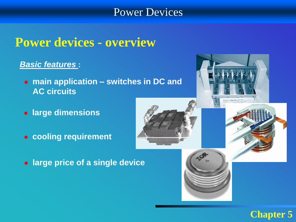
Power Devices
Chapter 5
Power devices - overview
Basic features :
● main application – switches in DC and
AC circuits
● large dimensions
● cooling requirement
● large price of a single device
Power Devices
Chapter 5
Power devices - overview
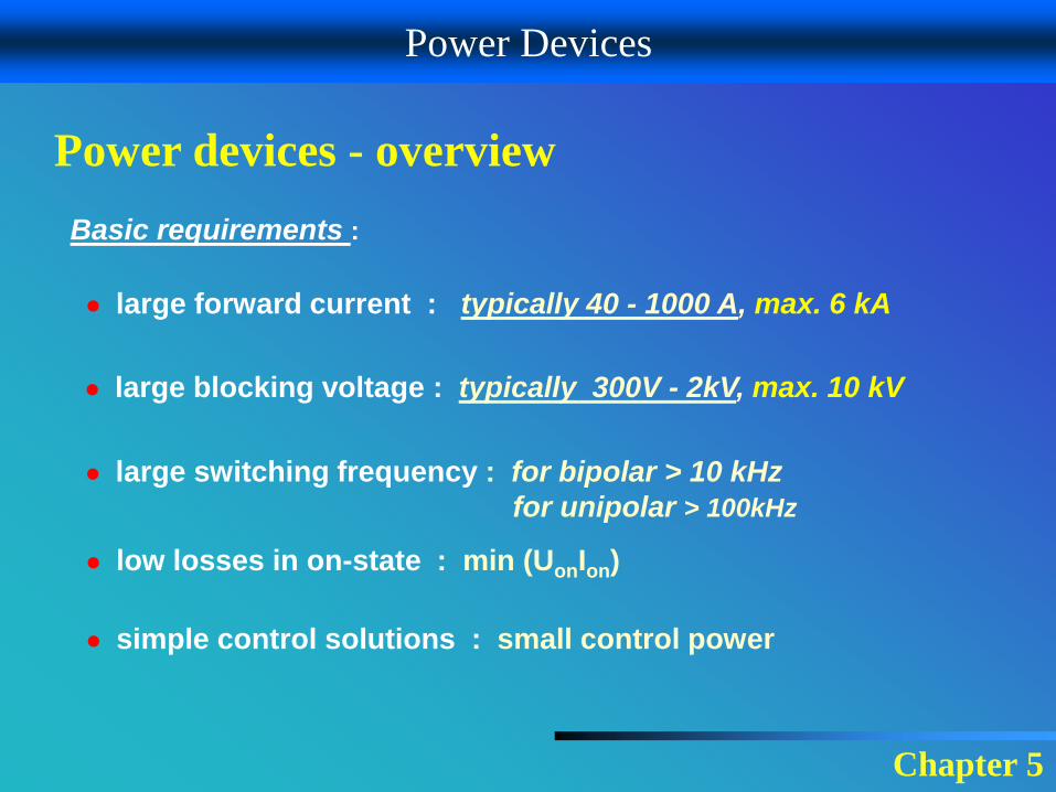
Basic requirements :
● large forward current : typically 40 - 1000 A, max. 6 kA
● large blocking voltage : typically 300V - 2kV, max. 10 kV
● large switching frequency : for bipolar > 10 kHz
for unipolar > 100kHz
● low losses in on-state : min (UonIon)
● simple control solutions : small control power
Power Devices
Chapter 5
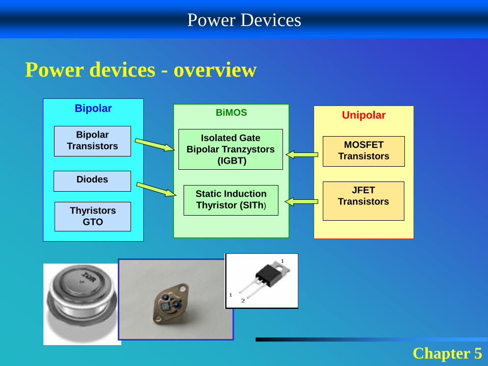
Bipolar
Diodes
Bipolar
Transistors
Thyristors
GTO
Unipolar
MOSFET
Transistors
JFET
Transistors
BiMOS
Isolated Gate
Bipolar Tranzystors
(IGBT)
Static Induction
Thyristor (SITh)
Power devices - overview
Power Devices - Thyristor
Chapter 5
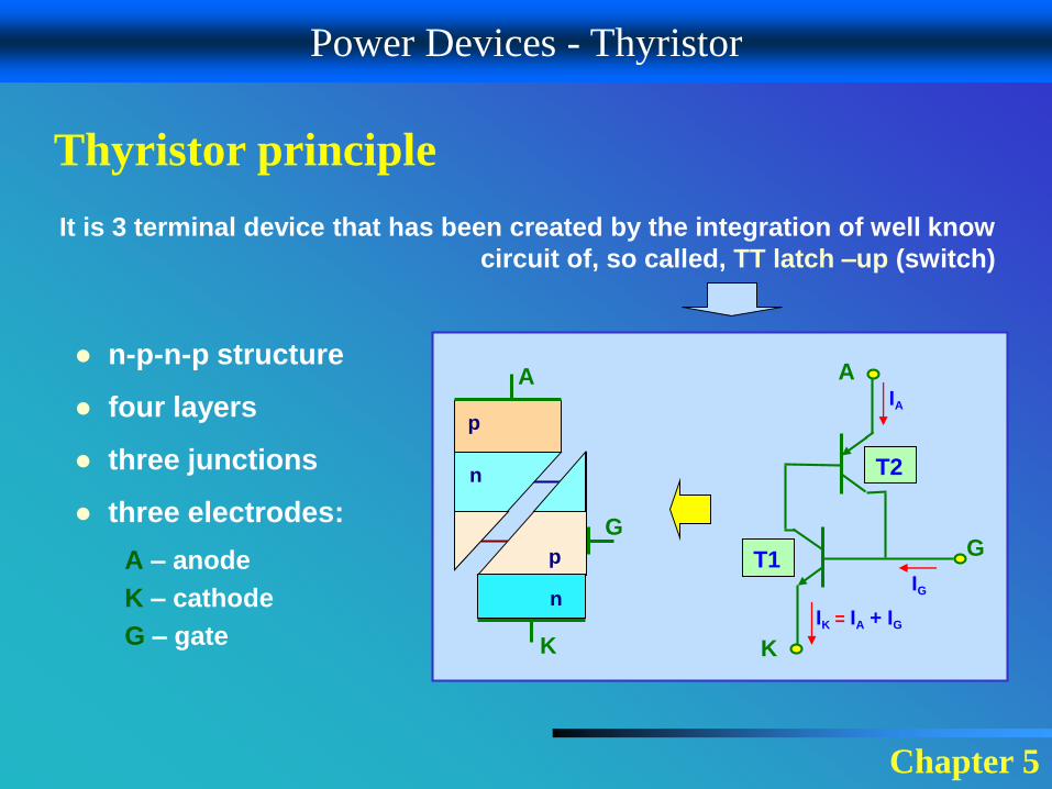
Thyristor principle
It is 3 terminal device that has been created by the integration of well know
circuit of, so called, TT latch –up (switch)
G
A
K
n
n
p
p
A
K
G
IA
T1
T2
IG
IK = IA + IG
● n-p-n-p structure
● four layers
● three junctions
● three electrodes:
A – anode
K – cathode
G – gate
Power Devices - Thyristor
Chapter 5
Work principle
G
A
K
n
n
p
p
A
K
G
IA
T1
T2
IG
IK = IA + IG
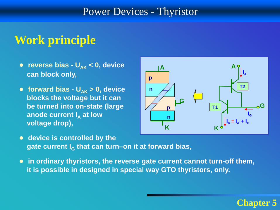
● reverse bias - UAK < 0, device
can block only,
● forward bias - UAK > 0, device
blocks the voltage but it can
be turned into on-state (large
anode current IA at low
voltage drop),
● device is controlled by the
gate current IG that can turn–on it at forward bias,
● in ordinary thyristors, the reverse gate current cannot turn-off them,
it is possible in designed in special way GTO thyristors, only.
Power Devices - Thyristor
Chapter 5
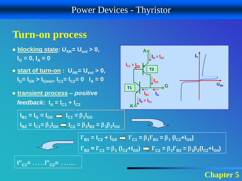
Turn-on process
A
K
G
IA = IE2
IC1 = IB2
T1
T2
IC2
IB1 IG
IK = IE1
UAK
IT
● blocking state: UAK= Uext > 0,
IG = 0, IA = 0
● start of turn-on : UAK= Uext > 0,
IG= IG0 > IGmin, IC1= IC2= 0 IA = 0
● transient process – positive
feedback: IA = IC1 + IC2
IB1 = IG = IG0 IC1 = 1IG0
IB2 = IC1= 1IG0 IC2 = 2IB2 = 12IG0
I’B1 = IC2 + IG0 I’C1 = 1I’B1 = 1 (IC2+IG0)
I’B2 = I’C1 = 1 (IC2+IG0) I’C2 = 2I’B2 = 12(IC2+IG0)
I’’C1= …..I’’C2= …...
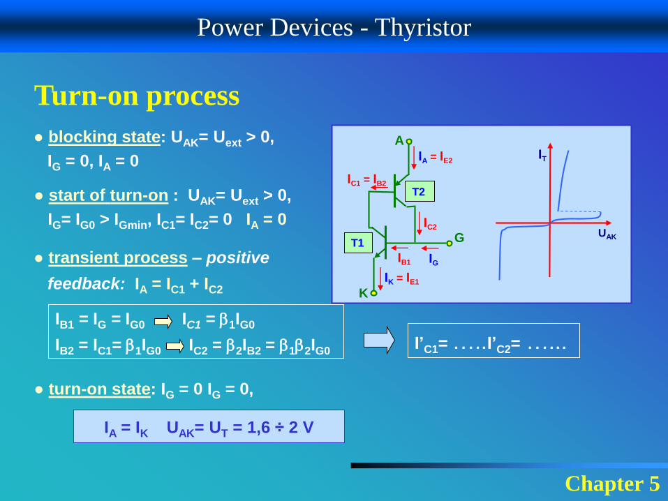
Power Devices - Thyristor
Chapter 5
Turn-on process
A
K
G
IA = IE2
IC1 = IB2
T1
T2
IC2
IB1 IG
IK = IE1
UAK
IT
● blocking state: UAK= Uext > 0,
IG = 0, IA = 0
● start of turn-on : UAK= Uext > 0,
IG= IG0 > IGmin, IC1= IC2= 0 IA = 0
● transient process – positive
feedback: IA = IC1 + IC2
IB1 = IG = IG0 IC1 = 1IG0
IB2 = IC1= 1IG0 IC2 = 2IB2 = 12IG0
● turn-on state: IG = 0 IG = 0,
IA = IK UAK= UT = 1,6 ÷ 2 V
I’C1= …..I’C2= …...
Power Devices - Thyristor
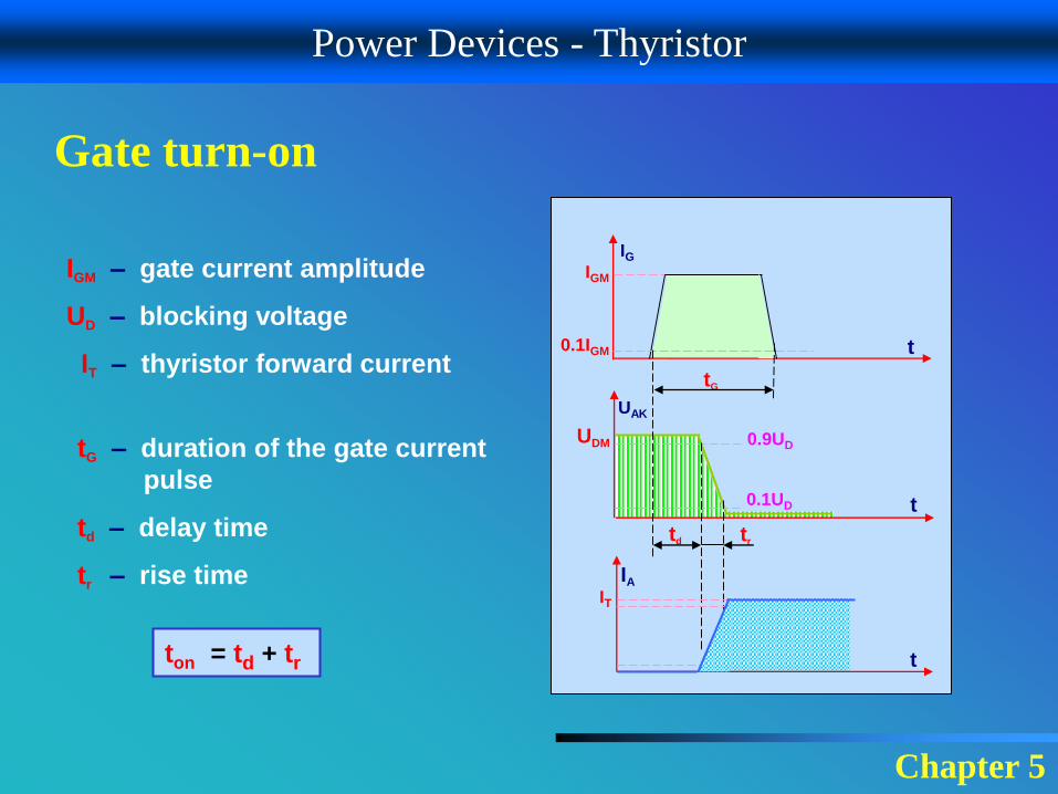
Chapter 5
Gate turn-on
t
t
t
IT
IA
0.1UD
0.9UDUDM
UAK
0.1IGM
IGM
IG
tG
trtd
IGM – gate current amplitude
UD – blocking voltage
IT – thyristor forward current
tG – duration of the gate current
pulse
td – delay time
tr – rise time
ton = td + tr
Power Devices - Thyristor
Chapter 5
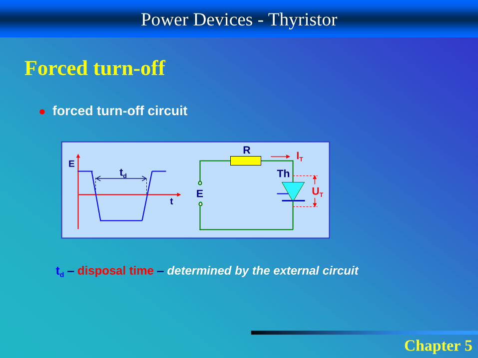
Forced turn-off
● forced turn-off circuit
td
E
t
RIT
UT
Th
E
td – disposal time – determined by the external circuit
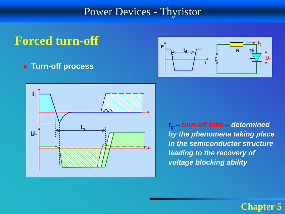
Power Devices - Thyristor
Chapter 5
Forced turn-off
● Turn-off process
td
E
t
R
IT
UT
Th
E
tq – turn-off time – determined
by the phenomena taking place
in the semiconductor structure
leading to the recovery of
voltage blocking ability
IT
tq
UT
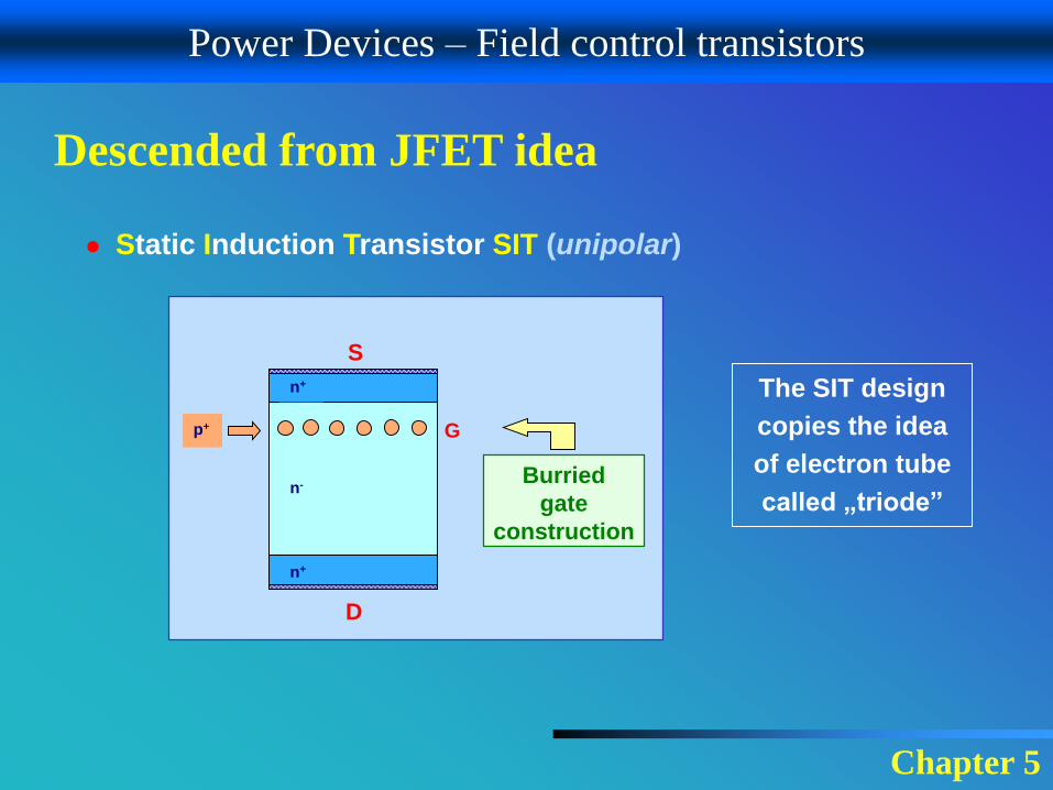
Power Devices – Field control transistors
Chapter 5
Descended from JFET idea
● Static Induction Transistor SIT (unipolar)
Burried
gate
construction
S
D
G
n+
n+
n-
p+
The SIT design
copies the idea
of electron tube
called „triode”
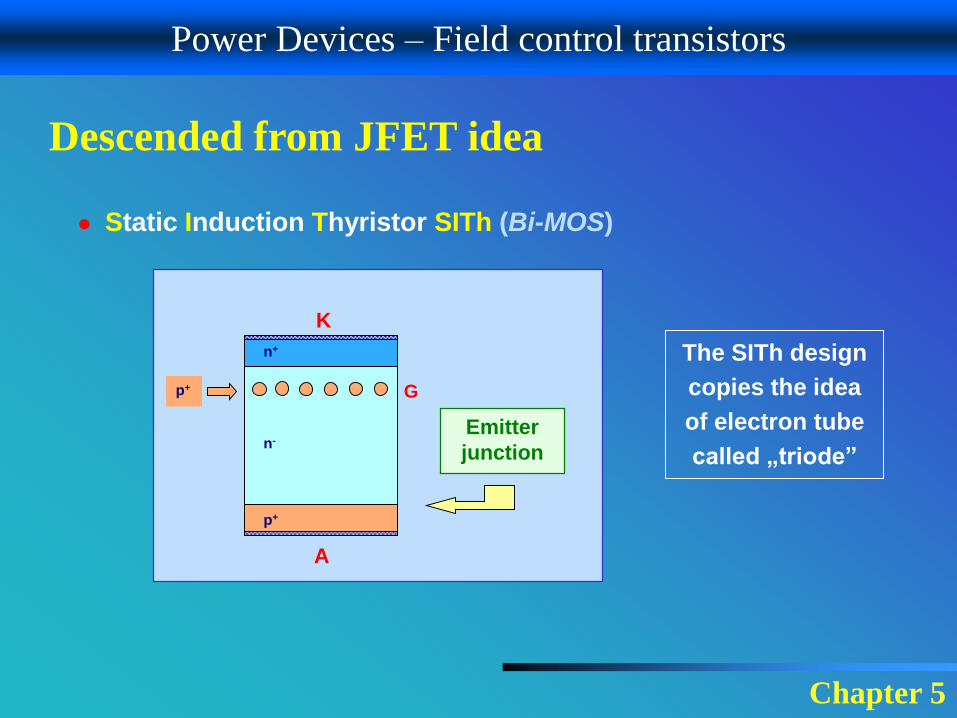
Power Devices – Field control transistors
Chapter 5
Descended from JFET idea
● Static Induction Thyristor SITh (Bi-MOS)
Emitter
junction
K
A
G
n+
p+
n-
p+
The SITh design
copies the idea
of electron tube
called „triode”
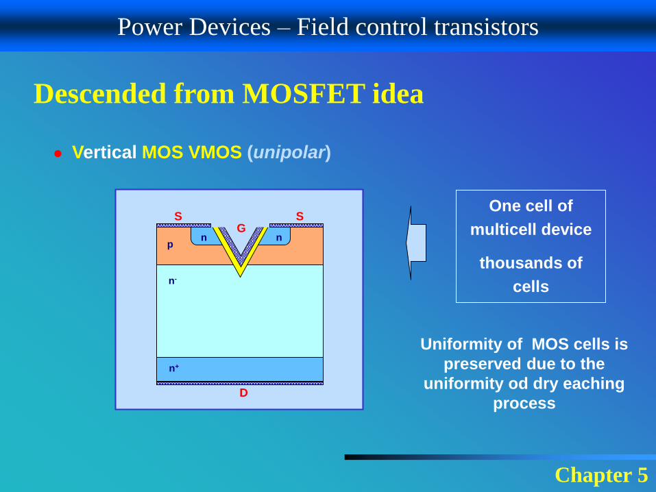
Power Devices – Field control transistors
Chapter 5
Descended from MOSFET idea
● Vertical MOS VMOS (unipolar)
One cell of
multicell device
thousands of
cells
D
pn
n-
n+
GS
n
S
Uniformity of MOS cells is
preserved due to the
uniformity od dry eaching
process
Power Devices – Field control transistors
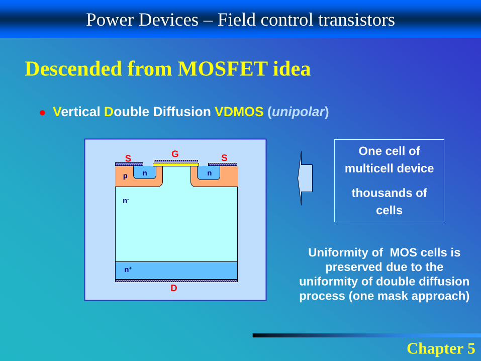
Chapter 5
Descended from MOSFET idea
● Vertical Double Diffusion VDMOS (unipolar)
One cell of
multicell device
thousands of
cells
Uniformity of MOS cells is
preserved due to the
uniformity of double diffusion
process (one mask approach)D
n-
n+
p n
GS S
n
Power Devices – Field control transistors
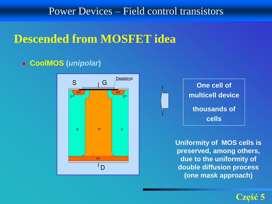
● CoolMOS (unipolar)
Część 5
Descended from MOSFET idea
One cell of
multicell device
thousands of
cells
Uniformity of MOS cells is
preserved, among others,
due to the uniformity of
double diffusion process
(one mask approach)
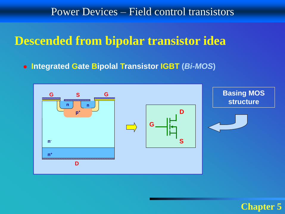
Power Devices – Field control transistors
Chapter 5
Descended from bipolar transistor idea
● Integrated Gate Bipolal Transistor IGBT (Bi-MOS)
G
S
D
D
n-
n+
p+
n
G S
n
G Basing MOS
structure
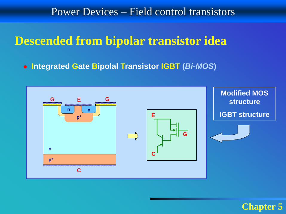
Power Devices – Field control transistors
Chapter 5
Descended from bipolar transistor idea
● Integrated Gate Bipolal Transistor IGBT (Bi-MOS)
Modified MOS
structure
IGBT structure
C
n-
p+
p+
n
G E
n
G
G
E
C
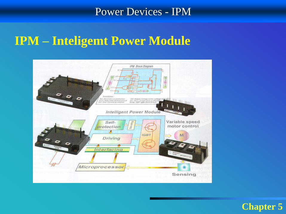
Power Devices - IPM
Chapter 5
IPM – Inteligemt Power Module


![Semiconductor Devices [Kanaan Kano]](https://img.pdfslide.us/doc/110x75/55cf931a550346f57b9bb747/semiconductor-devices-kanaan-kano.jpg)