Embed Size (px)
Citation preview
Wed. Oct. 5th, 2016
Semiconductor Devices (EE336)
Lec. 2: Energy Bands and Charge Carriers
Dr. Mohamed Hamdy Osman
2
Lecture Outline
What is a semiconductor? & Semiconductor materials Electronic configuration of Si atom Si crystal and covalent bonding Formation of energy bands and gaps in solid crystals Energy band diagram and measurement of energy gap Metals, insulators and semiconductors
3
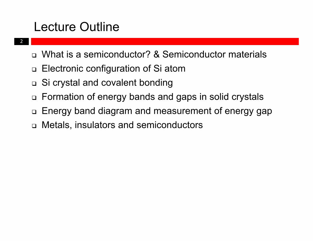
What is a semiconductor?
Low resistivity “conductor” High resistivity “insulator” Intermediate resistivity “semiconductor”
The conductivity (S/m) and at the same time the resistivity of semiconductors lies between that of conductors and insulators.
4
What is a semiconductor?
No recognizablelong-range order
Completely orderedin segments
Entire solid is made up of atoms in an orderly
three- dimensional array
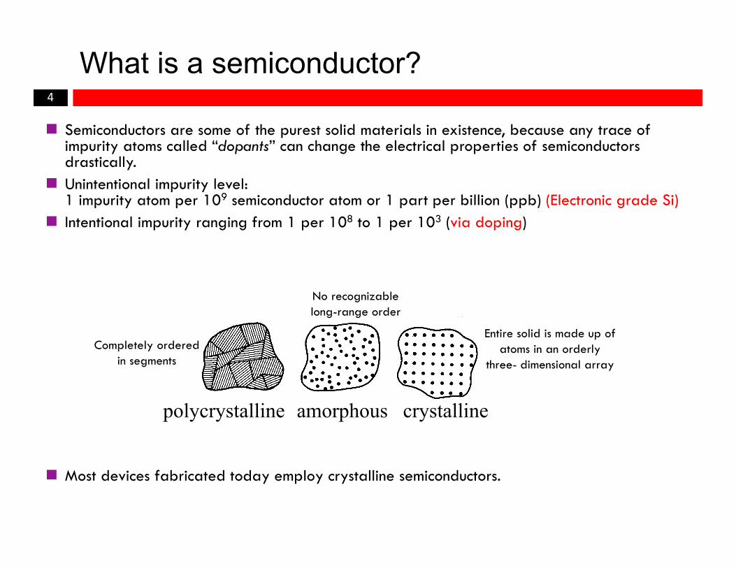
Semiconductors are some of the purest solid materials in existence, because any trace of impurity atoms called “dopants” can change the electrical properties of semiconductors drastically.
Unintentional impurity level: 1 impurity atom per 109 semiconductor atom or 1 part per billion (ppb) (Electronic grade Si)
Intentional impurity ranging from 1 per 108 to 1 per 103 (via doping)
Most devices fabricated today employ crystalline semiconductors.
polycrystalline amorphous crystalline
5
Semiconductor materials
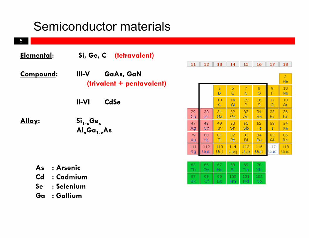
Elemental: Si, Ge, C (tetravalent)
Compound: III-V GaAs, GaN (trivalent + pentavalent)
II-VI CdSe
Alloy: Si1-xGexAlxGa1-xAs
As : ArsenicCd : CadmiumSe : SeleniumGa : Gallium
6
Recall four quantum numbers
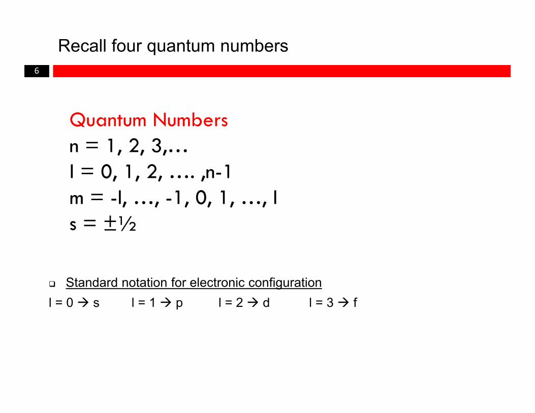
Quantum Numbersn = 1, 2, 3,…l = 0, 1, 2, …. ,n-1m = -l, …, -1, 0, 1, …, ls = ±½
Standard notation for electronic configurationl = 0 s l = 1 p l = 2 d l = 3 f
7
Electronic configuration of Si
+14 Nucleus
Inner Orbits(10 core electrons)
Valence Orbits(4 valence electrons)
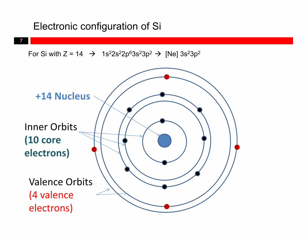
For Si with Z = 14 1s22s22p63s23p2 [Ne] 3s23p2
8
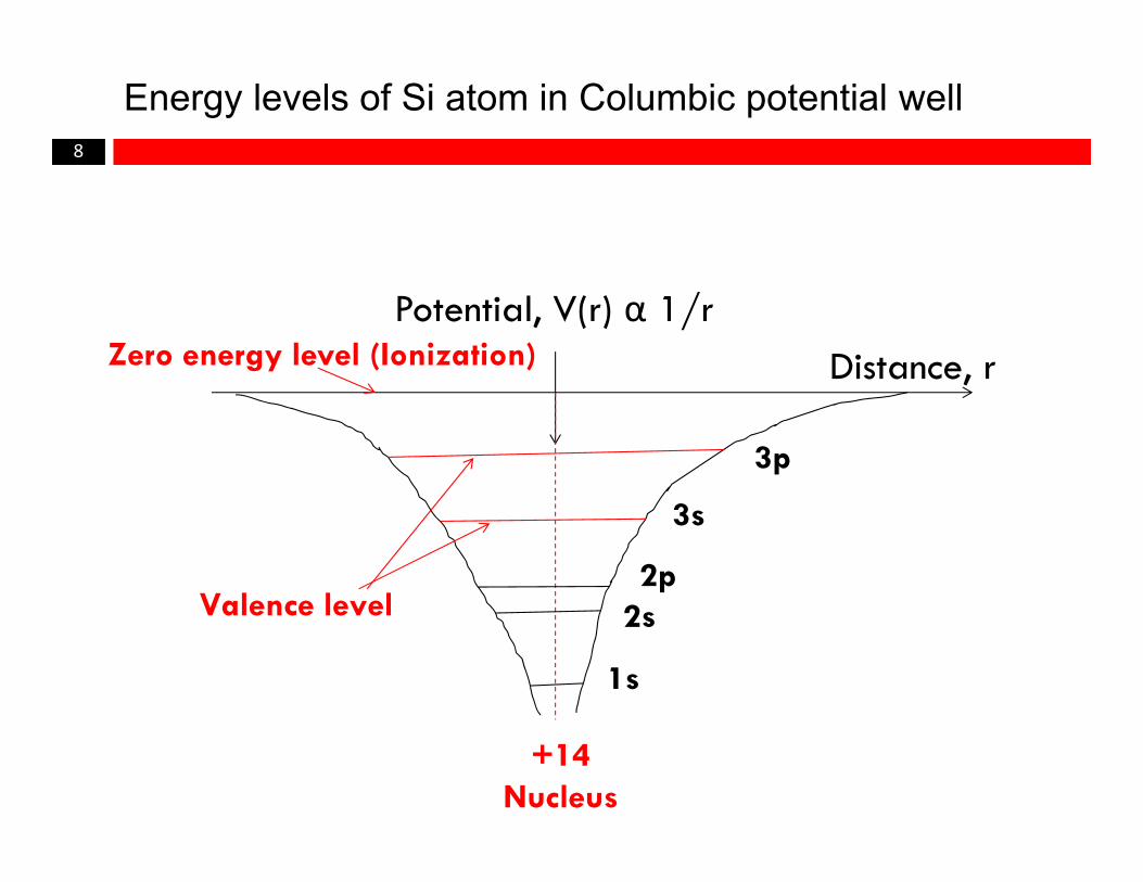
Energy levels of Si atom in Columbic potential well
Distance, rPotential, V(r) α 1/r
Zero energy level (Ionization)
Valence level
3p
3s
2p2s
1s
+14Nucleus
9
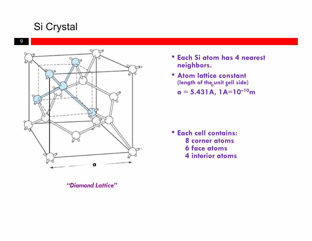
Si Crystal
“Diamond Lattice”
a
• Each Si atom has 4 nearest neighbors.
• Atom lattice constant(length of the unit cell side)
a = 5.431A, 1A=10–10m° °
• Each cell contains: 8 corner atoms6 face atoms4 interior atoms
10
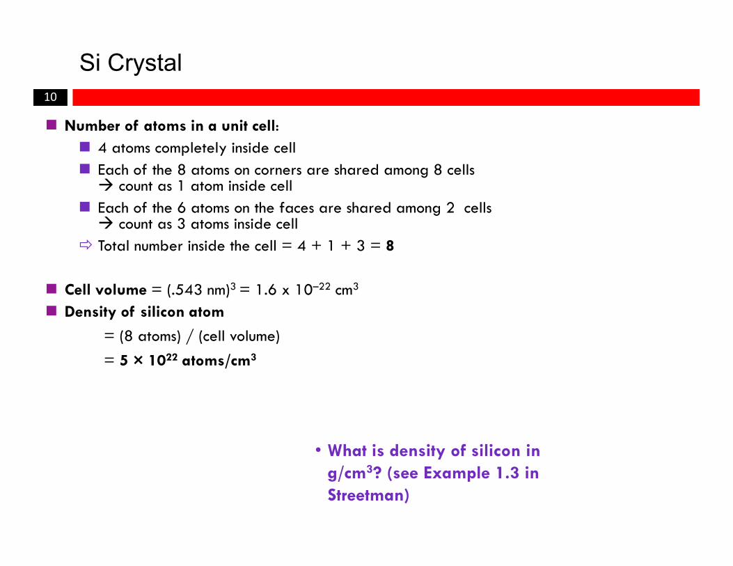
Si Crystal
Number of atoms in a unit cell: 4 atoms completely inside cell Each of the 8 atoms on corners are shared among 8 cells count as 1 atom inside cell
Each of the 6 atoms on the faces are shared among 2 cells count as 3 atoms inside cell
Total number inside the cell = 4 + 1 + 3 = 8
Cell volume = (.543 nm)3 = 1.6 x 10⁻²² cm3
Density of silicon atom
= (8 atoms) / (cell volume) = 5 × 10²² atoms/cm3
• What is density of silicon in g/cm3? (see Example 1.3 in Streetman)
11
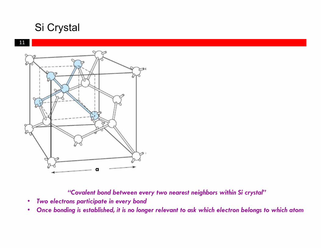
Si Crystal
“Covalent bond between every two nearest neighbors within Si crystal”• Two electrons participate in every bond• Once bonding is established, it is no longer relevant to ask which electron belongs to which atom
a
12
Why chemical bonding occurs and what happens?
• A chemical bond is an increase in electron density along or to the sides of the connecting line between the nuclei
• There are different types of bonding such as ionic bonding, covalent bonding, etc.
• In order for a chemical bond to be stable, there must be energy favoring compared to the case where bonding does not occur, i.e. electrons constituting the bond will fill lower energy levels relative to the isolated case
• In order to qualitatively understand why bonding occurs, we will use the concept of hybridization via linear combination of atomic orbitals (LCAO)
13
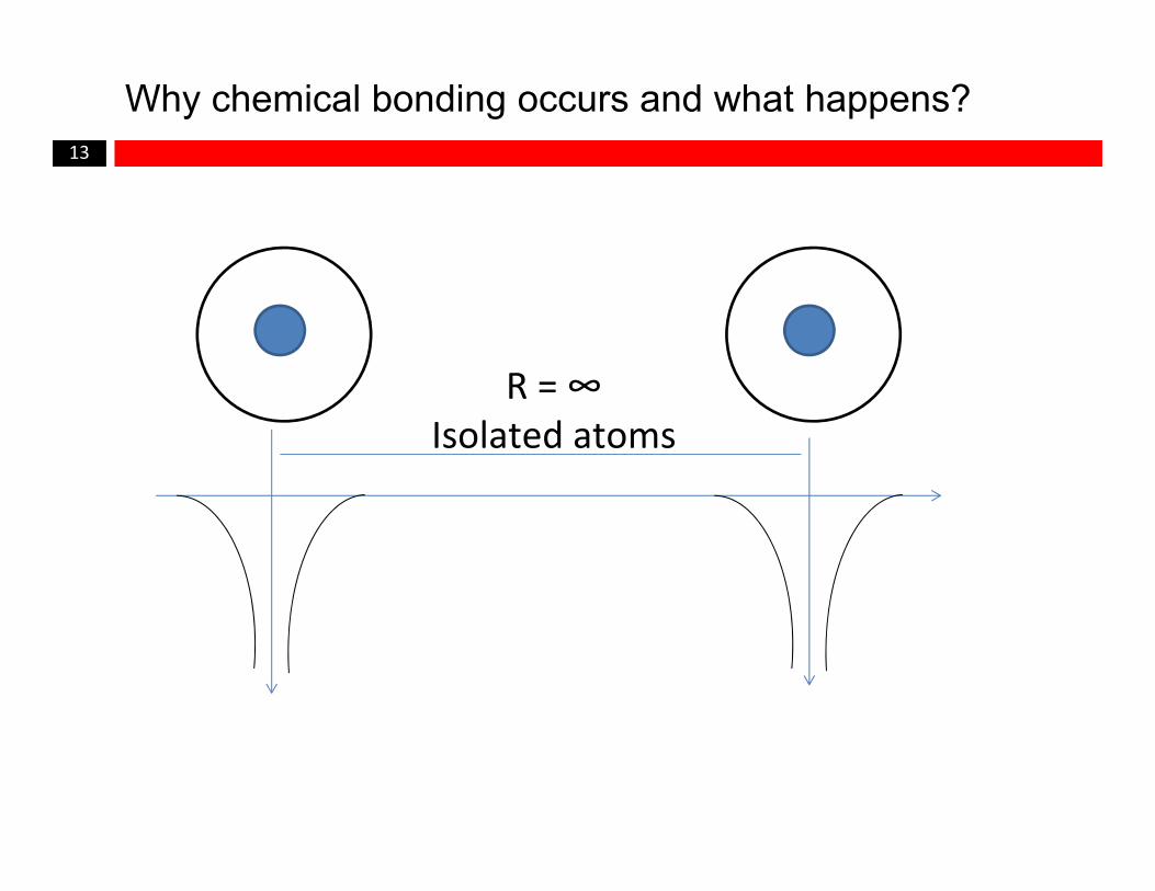
Why chemical bonding occurs and what happens?
R = ∞Isolated atoms
14
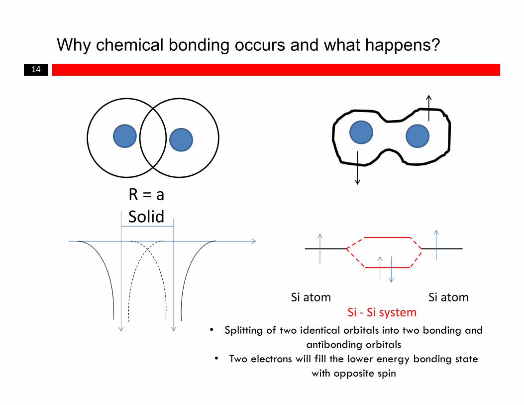
Why chemical bonding occurs and what happens?
R = aSolid
Si atomSi atomSi ‐ Si system
• Splitting of two identical orbitals into two bonding and antibonding orbitals
• Two electrons will fill the lower energy bonding state with opposite spin
15
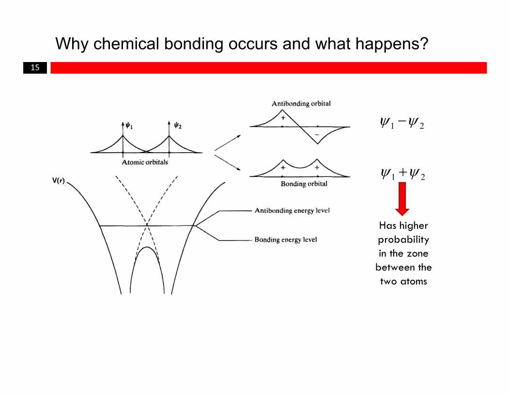
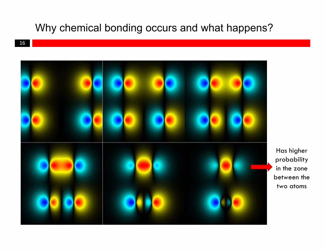
Why chemical bonding occurs and what happens?
21
21
Has higher probability in the zone
between the two atoms
16
Why chemical bonding occurs and what happens?
Has higher probability in the zone
between the two atoms
17
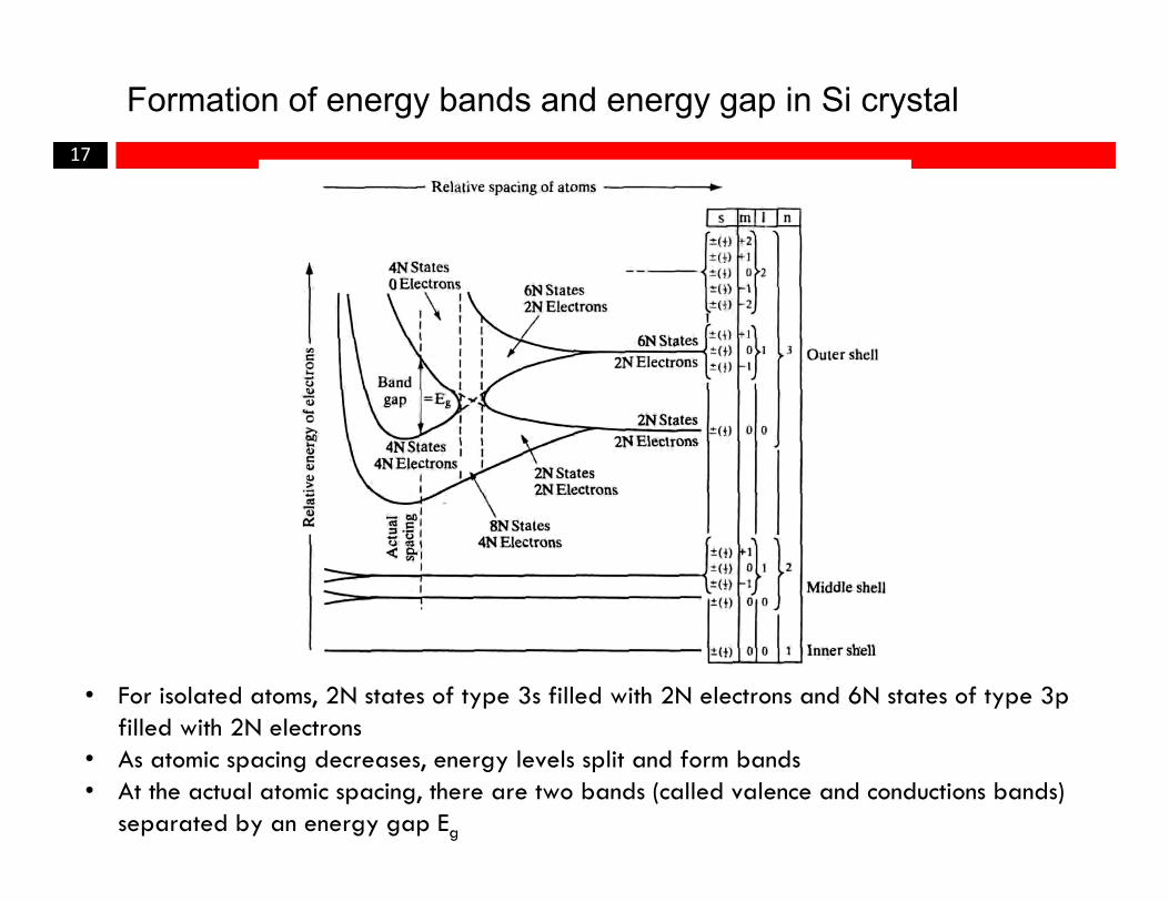
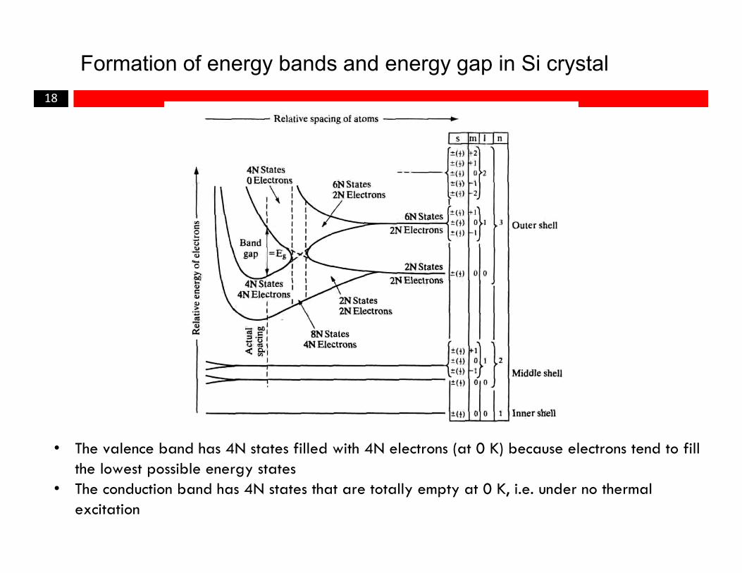
Formation of energy bands and energy gap in Si crystal
• For isolated atoms, 2N states of type 3s filled with 2N electrons and 6N states of type 3p filled with 2N electrons
• As atomic spacing decreases, energy levels split and form bands• At the actual atomic spacing, there are two bands (called valence and conductions bands)
separated by an energy gap Eg
18
Formation of energy bands and energy gap in Si crystal
• The valence band has 4N states filled with 4N electrons (at 0 K) because electrons tend to fill the lowest possible energy states
• The conduction band has 4N states that are totally empty at 0 K, i.e. under no thermal excitation
19
V(x)
V0
Formation of energy bands and energy gap in Si crystal
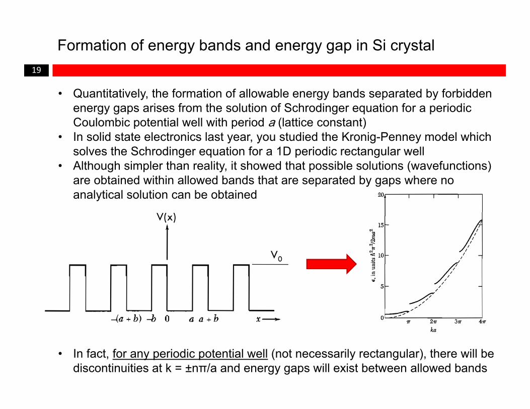
• Quantitatively, the formation of allowable energy bands separated by forbidden energy gaps arises from the solution of Schrodinger equation for a periodic Coulombic potential well with period a (lattice constant)
• In solid state electronics last year, you studied the Kronig-Penney model which solves the Schrodinger equation for a 1D periodic rectangular well
• Although simpler than reality, it showed that possible solutions (wavefunctions) are obtained within allowed bands that are separated by gaps where no analytical solution can be obtained
• In fact, for any periodic potential well (not necessarily rectangular), there will be discontinuities at k = ±nπ/a and energy gaps will exist between allowed bands
20
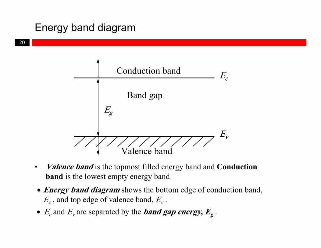
Energy band diagram
Conduction band Ec
Ev
Eg
Band gap
Valence band
Energy band diagram shows the bottom edge of conduction band, Ec , and top edge of valence band, Ev .
Ec and Ev are separated by the band gap energy, Eg .
• Valence band is the topmost filled energy band and Conduction band is the lowest empty energy band
21
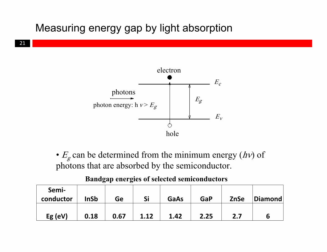
Measuring energy gap by light absorption
photons
photon energy: h v > Eg
Ec
Ev
Eg
electron
hole
Bandgap energies of selected semiconductors
• Eg can be determined from the minimum energy (h) of photons that are absorbed by the semiconductor.
Semi‐conductor InSb Ge Si GaAs GaP ZnSe Diamond
Eg (eV) 0.18 0.67 1.12 1.42 2.25 2.7 6
22
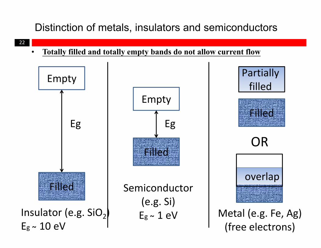
Distinction of metals, insulators and semiconductors
Filled
Empty
Eg
Insulator (e.g. SiO2)Eg ̴ 10 eV
Filled
Empty
Eg
Semiconductor (e.g. Si)Eg ̴ 1 eV
Filled
Partially filled
overlap
Metal (e.g. Fe, Ag)(free electrons)
OR
• Totally filled and totally empty bands do not allow current flow
23
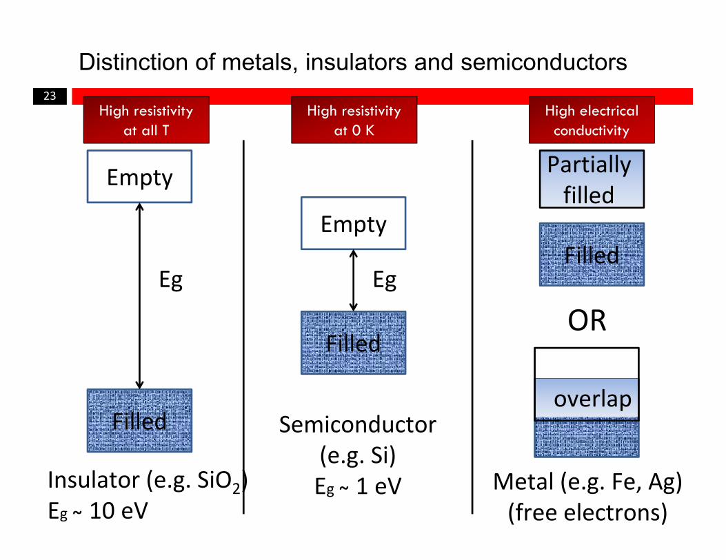
Distinction of metals, insulators and semiconductors
Filled
Empty
Eg
Insulator (e.g. SiO2)Eg ̴ 10 eV
Filled
Empty
Eg
Semiconductor (e.g. Si)Eg ̴ 1 eV
Filled
Partially filled
overlap
Metal (e.g. Fe, Ag)(free electrons)
OR
High resistivity at 0 K
High electrical conductivity
High resistivity at all T
24
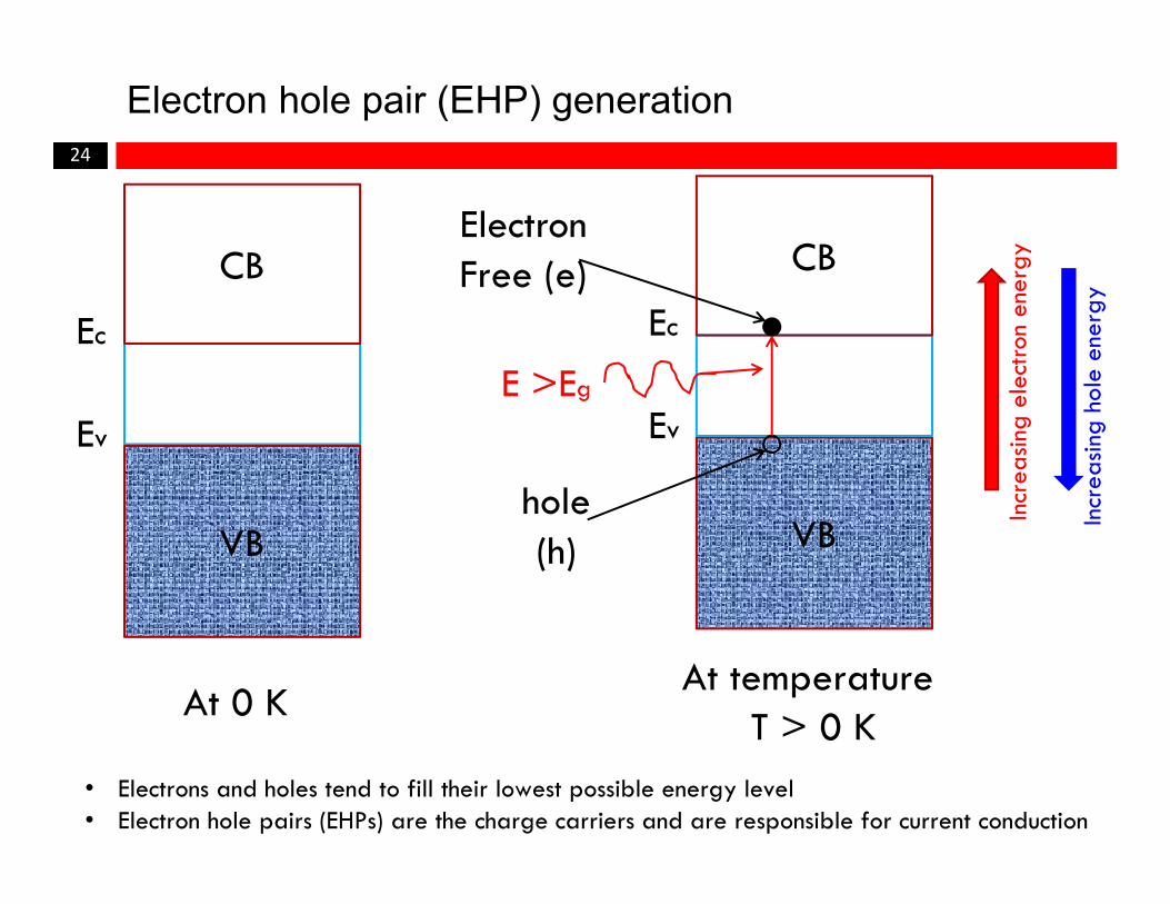
Electron hole pair (EHP) generation
VBVB
CB
Ec
Ev
At 0 K
CB
Ec
Ev
At temperature T > 0 K
ElectronFree (e)
hole(h)
E >Eg
Incr
easin
g el
ectro
n en
ergy
Incr
easin
g ho
le e
nerg
y
• Electrons and holes tend to fill their lowest possible energy level• Electron hole pairs (EHPs) are the charge carriers and are responsible for current conduction