Embed Size (px)
Citation preview

Self-Powered Wireless Sensor Module
Submitted by Eu Jin Ooi on 9 September 2013
Supervised by Ridha Ben Mrad

Page 1 of 32
1. Introduction
A self-powered wireless sensor module is developed in this project. The module will periodically
enter an operational mode where it gathers data from its sensors, and then transmit the data to a
receiver via its wireless module. While not operating, it will be put on standby mode to reduce
power consumption. It will be powered by a piezoceramic energy harvester which gathers and
stores energy through motion (humans, vehicles and wind).
It is made up of two main components, i.e., the loading unit and the supply unit. The loading unit
consists of a microcontroller, sensors and a wireless module for data transmission. The supply
unit primarily consists of a piezoceramic energy harvester and its conditioning circuitry.
2. Objectives
The wireless sensor module should meet the following objectives:
1. Reliable: Long product lifetime
2. Portable: Small and light
3. Durable: Should not be affected by wear and tear
4. Long working range of data transmission
3. Applications
The self-powered module can be applied for various applications based on the type of sensors
used. This technology can be applied in three main fields: structural health monitoring, human
tracking and animal tracking.
4. Electrical Design
The wireless sensor module is divided into two main components:
1. Loading unit: microcontroller, sensors, wireless module
2. Supply unit: piezoceramic energy harvester, conditioning circuitry
In this section, the designs for both units are discussed. At the end of this section, printed circuit
board (PCB) designs used to miniaturize the modules are shown.
4.1. Loading Unit
For the loading unit, two designs were developed. Design 1 integrates off-the-shelf electronics to
demonstrate the ability to produce a wireless sensor module. Design 2 integrates low power
electronics to allow the module to be self-powered.
4.1.1. Design 1: Off-the-shelf Electronics
Off-the-shelf electronics are integrated as a proof-of-concept that an idea of a wireless sensor
module is reasonable. The following are the products used:
1. Microcontroller: Arduino Fio board (ATmega328P)

Page 2 of 32
2. Sensors: Infrared thermometer (MLX90614), Pulse sensor
3. Radio module: XBee Series 1 running on IEEE 802.15.4 wireless standard
Initially, the Arduino Uno was used as the microcontroller board due to its simplicity. However,
due to its large size and higher power consumption (DC current of 50mA per pin, at an operating
voltage of 5V [1]), it is replaced by the Arduino Fio (refer to Figure 1) for Design 1.
Figure 1: Arduino Fio [2]
Table 1 shows a summary of Arduino Fio’s datasheet.
Table 1: Summary of Arduino Fio’s datasheet [2]
Microcontroller ATmega328P
Operating Voltage 3.3V
Input Voltage 3.35 -12 V
Input Voltage for Charge 3.7 - 7 V
Digital I/O Pins 14 (of which 6 provide 8-bit PWM output)
Analog Input Pins 8 (10-bit resolution)
DC Current per I/O Pin 40 mA
Flash Memory 32 KB (of which 2 KB used by bootloader)
SRAM 2 KB
EEPROM 1 KB
Clock Speed 8 MHz
MLX90614 (shown on Figure 2) is a non-contact infrared thermometer which has an internal 17-
bit analog-to-digital converter. Inter-integrated circuit (I2C 2-wire serial bus) is used to
communicate between the microcontroller and the MLX90614.

Page 3 of 32
Figure 2: Infrared thermometer [3]
Table 2 shows a summary of MLX90614’s datasheet.
Table 2: Summary of MLX90614’s datasheet [3]
Thermometer MLX90614
Supply Voltage 3.6V to 5V
Reverse Voltage 0.4V
Operating Temperature Range -40℃ to +85℃
DC Operating Current (maximum) 25mA
The pulse sensor (shown on Figure 3) is an open source hardware which is available through
Sparkfun. It runs on voltages from 3V to 5V and consumes 4mA at 5V. As an optical pulse
sensor, it emits light into a finger tip. The light will then either be reflected by the skin tissues or
absorbed by the blood cells. The time between the two occurrences of light absorption is defined
as a single heart beat.
Figure 3: Pulse sensor [4]
XBee Series 1 (refer to Figure 4) is a 2.4GHz wireless module with a PCB trace antenna which
runs on the IEEE 802.15.4 or ZigBee standard. It has 8 digital input-output pins and 6 10-bit
analog-to-digital input pins. The transmitter on the module is made to communicate serially to
the receiver on a separate unit at a 57600 baud rate. Table 3 shows a summary of XBee Series
1’s datasheet.

Page 4 of 32
Figure 4: XBee Series 1
Table 3: Summary of XBee Series 1
Wireless Module XBee Series 1
Supply Voltage 3.3V
DC Operating Current 50mA
Data Transmission Range 100m
Power Output 1mW
The design is powered using a 3.7V lithium-ion battery. The microcontroller is programmed
using the Arduino Integrated Drive Electronics (IDE) standard which is based on a modified C or
“wiring” programming language (part of the code shown on Figure 5). Interrupt service routines
are used to enable low power modes and re-activating the module through a microswitch.
Figure 5: Part of the code used for Design 1

Page 5 of 32
The logic used in programming the microcontroller for Design 1 is shown on Figure 6.
Measure Temperature
Measure Pulse Transmit DataSTARTSTANDBY-MODE
Wait for Interrupt
Interrupt Through Microswitch
Figure 6: Flow chart for Design 1 programming logic
Based on the power requirement tests, it is determined that the loading circuit powered by the
3.7V lithium-ion battery consumes 3.1mA (11.47mW) on standby mode and 64.6mA
(239.02mW) on operational mode (shown on Figure 7).
Figure 7: Power requirement tests (left: standby mode, right: operational mode)
The current state-of-the-art piezoceramic energy harvester is capable of generating 100𝜇W from
a body vibrating at a constant 1g or 9.81m/s2 acceleration. Since power consumption by this
design cannot be sustained by the energy harvester, it is required to seek low-power electronics.
4.1.2. Design 2: Low-power Electronics
Based on the issues faced in Design 1, it is required for Design 2 to consume less power in order
to meet the capabilities of the piezoceramic energy harvester. The frequency of data transmission
by the module will be governed by the ratio of power consumptions during operational mode and
during standby mode.
The low-power microcontrollers and radio frequency modules available in the market are shown
on Table 4 and Table 5.

Page 6 of 32
Table 4: Low-power microcontrollers
Company Part
Number Flash (kB) I/O ports Operating
Power (mW) Shut-down
Power (uW)
Texas Instruments MSP430G2 16 16 1.386 1.65
Microchip PIC12F1822 8 11 1.728 0.036
ST Microelectronics STM8L101 8 30 2.31 1.155
Lapis Semiconductor ML610Q421 32 22 8.25 1.65
Silicon Labs C8051F91 16 16 12.9 1.98
Table 5: Low-power radio frequency modules
Company Part
Number Frequency Range Operating
Power (mW) Shut-down
Power (uW)
Linx Technologies LR Series 433MHz 1km 5.94 16.5
RF Monolithics TRC104 2.4GHz <100m 27 1.32
Semtech SX1240 434/868MHz n/a 29.7 3.3
RF Monolithics XDM2140 2.4GHz <100m 54 28
RF Solutions TRX433 434/868/915 n/a 42.9 0.99
Current state-of-the-art low-power sensors are also looked into to improve the module’s
feasibility, as shown on Table 6 to Table 9.
Table 6: Low-power thermometers
Company Part
Number Output
(bits) Measurement
Range (C) Accuracy
Operating
Power
(uW)
Shut-
down
Power
(uW)
Texas Instruments TMP20 Analog -55 to 130 2.5 19.8 0.066 ST
Microelectronics STLM20 Analog -55 to 130 1.5 26.4 0.066
Microchip MCP9700 Analog -40 to 150 2 39.6 n/a ST
Microelectronics STTS75 Digital (9 to
12) -55 to 125 0.5 330 3.3
Texas Instruments TMP006 Digital (16) -40 to 125 n/a 1070 3.3

Page 7 of 32
Table 7: Low-power accelerometers
Company Part
Number # of Axis Measurement
Range (g) Sensitivity
(mg/LSB)
Operating
Power
(uW)
Shut-
down
Power
(uW)
Analog Devices ADXL362 3 2/4/8 1/2/4 5.9 0.033
Kionix KX023 3 2/4/8 1/2/4 33 6.6 ST
Microelectronics LIS3DH 3 2/4/8/16 1/2/4/12 36.3 1.65
Freescale MMA8450Q 3 2/4/8 1/2/4 138.6 3.3
Note: Data is for 50Hz operation
Table 8: Low-power gyroscope
Company Part
Number # of
Axis Measurement
Range (dps) Sensitivity
(mdps/LSB)
Operating
Power
(mW)
Shut-
down
Power
(mW) Maxim
Integrated MAX21000 3 500/1000/2000 16.7/33.3/66.7 17.82 0.028
InvenSense MPU3000 3 250/500/1000/2000 7.6/15.0/30.5/61.0 20.13 0.0165 ST
Microelectronics L3G4200D 3 250/500/2000 8.75/17.5/70 20.13 0.0165 Analog Devices ADXRS450 1 300 12.5 33 n/a Analog Devices ADIS16260 1 80/160/320 18.3/36.6/73.3 135.3 1.16
Note: dps: degrees/second; LSB: least significant bit
Table 9: Low-power GPS
Company Part
Number
Horizontal
Accuracy 90%
(m)
Altitude
Accuracy
90% (m) Operating
Power (mW)
Shut-down
Power
(mW)
Fastrax IT430 n/a n/a 68 0.036
Trimble Copernicus
2 4 5 132 0.0396
Trimble Lassen LP 9 18 221 24
The microcontroller, radio frequency module and sensors with the lowest operating power
consumptions are chosen for Design 2. Thermometers and accelerometers are chosen to be
integrated due to their relatively lower power consumptions compared to the other sensors. The
theoretical total power consumption by Design 2, integrating the chosen electronics is shown on
Table 10.

Page 8 of 32
Table 10: Total power consumption by Design 2
Component Company Operating Power Standby Power
Microcontroller Texas Instruments 1.386mW 1.65𝜇W
Thermometer Texas Instruments 19.8𝜇W 0.066𝜇W
Accelerometer Analog Devices 5.9𝜇W 0.033𝜇W
RF module (Transmitter) Linx Technologies 5.94mW 16.5𝜇W
Total 7.3517mW 18.249𝜇W
MSP430 Texas LaunchPad (refer to Figure 8) is used as the microcontroller board for
prototyping development purpose. The microcontroller (MSP430G2553) is programmed using
this board via USB serial communication.
Figure 8: MSP430 Texas LaunchPad [5]
MSP430G2553 is programmed using the Energia IDE, which is based on modified C or “wiring”
language (part of the code shown on Figure 9). Testing and evaluation of the program can be
done on the board itself which consists of voltage regulators, jumpers and male headers directly
connected to the pins of the microcontroller. The programmed microcontroller can then be
removed and plugged into a breadboard for further development. It is important to note that pin
XIN is programmed to be HIGH while pin XOUT is programmed to be LOW during operational
mode. These two pins are then used to provide power supply to the sensors and radio modules.
The microcontroller is initially integrated with the sensors, i.e., TMP20 which measures
temperature through contact and ADXL362 which measures tri-axial acceleration. Since TMP20
is a surface mount device (SMD), a breakout board is fabricated to enable prototyping using the
breadboard. Since breakout boards for ADXL362 are available in the market, additional
fabrication for this device is not required.
ADXL362 (refer to Figure 10) is a 12-bit digital accelerometer which communicates with the
microcontroller via the Serial Peripheral Interface (SPI) method. Using the SPI command, the

Page 9 of 32
range of ±2g is chosen for this application. It has a wide operating voltage range of 1.6V to 3.5V.
The pin connections from the breakout board to the microcontroller are shown on Table 11.
Figure 9: Part of the code used for Design 2
Figure 10: Digital accelerometer, ADXL362 [6]

Page 10 of 32
Table 11: Pin connections from ADXL362 to MSP430G2553
ADXL362 MSP430G2553
SCK Pin 1.5
MOSI Pin 1.7
MISO Pin 1.6
CS Pin 1.0
V+ XIN
GND XOUT
TMP20 (refer to Figure 11) is a precision analog output temperature sensor which operates from
-55℃ to +130℃ on a supply voltage of 2.7V to 5.5V. The pin connections from the breakout
board of TMP20 to the microcontroller are shown on Table 12.
Figure 11: Analog temperature sensor, TMP20
Table 12: Pin connections from TMP20 to MSP430G2553
TMP20 MSP430G2553
Analog VOut Pin 1.1
V+ XIN
GND (2) XOUT
The Linx Technologies LR Series Basic Evaluation kit (refer to Figure 12) is used to integrate
the radio module into Design 2. The kit includes a receiver module and a transmitter module.
The transmitter module is powered externally via the XIN and XOUT pins on the
microcontroller. The receiver module is also powered externally via another MSP430G2553
microcontroller to allow serial communication with the computer through the USB port.
Theoretically, the two modules are able to communicate up to a range of 1km. The antennas
included are external 433MHz antennas. The modules communicate via 8 digital bits (or 1 byte).
The pin connections from the transmitter module to the microcontroller are shown on Table 13.

Page 11 of 32
Figure 12: LR Series Basic Evaluation kit [7]
Table 13: Pin connections from LR Series transmitter to MSP430G2553
LR Series transmitter MSP430G2553
VCC XIN
GND XOUT
D0 – D5 Pin 2.0 – Pin 2.5
D6 Pin 1.3
D7 Pin 1.4
The 8 bits are utilized as shown on Table 14.
Table 14: 8-bit utilization
0 1 2 3 4 5 6 7
Alternate Data
Recognition
Single decimal digit of
data
A protocol is designed to ensure that the data transmitted is received correctly by the receiver. 4
bits (0, 1, 2 and 3) are used for this purpose. The first bit (Bit 0) will be alternately written 0 and
1 for subsequent data transmissions. Bits 1, 2, 3 are used to store binary digits converted from
decimal digits used for data recognition shown on Table 15.

Page 12 of 32
Table 15: Data recognition bits
Decimal Digit Binary Digits Representation
0 000 X-axis acceleration
1 001 Y-axis acceleration
2 010 Z-axis acceleration
3 011 Temperature
The transmitter transmits 4 data, i.e., accelerations in the X, Y and Z axes, and temperature.
Acceleration data have 4 decimal digits since the accelerometer have a 12-bit output resolution
(20 to 212 0 to 4096). Similarly, the temperature data have 4 decimal digits because TMP20’s
analog output is fed into MSP430G2553 microcontroller which uses a 10-bit analog-to-digital
converter for its Input/Output (I/O) pins (20 to 210 0 to 1024). A single decimal digit requires 4
bits for binary representation; thus, Bits 4 to 7 are used for this purpose.
In the first byte of a data, Bit 4 will be used to transmit the sign of the data, i.e., 1 for positive
and 0 for negative. Table 16 shows an example of the 4 distinct data being represented by 20
bytes.
Table 16: An example of the 8-bit representation of the data
Raw Data Represent Alternate Data Representation Single Decimal Digit
Bit 0 Bit 1 Bit 2 Bit 3 Bit 4 Bit 5 Bit 6 Bit 7
X-axis
acceleration
-0656
Negative 0 0 0 0 0
0 1 0 0 0 0 0 0 0
6 0 0 0 0 0 1 1 0
5 1 0 0 0 0 1 0 1
6 0 0 0 0 0 1 1 0
Y-axis
acceleration
-0077
Negative 1 0 0 1 0
0 0 0 0 1 0 0 0 0
0 1 0 0 1 0 0 0 0
7 0 0 0 1 0 1 1 1
7 1 0 0 1 0 1 1 1
Z-axis
acceleration
+1127
Positive 0 0 1 0 1
1 1 0 1 0 0 0 0 1
1 0 0 1 0 0 0 0 1
2 1 0 1 0 0 0 1 0
7 0 0 1 0 0 1 1 1
Temperature
+0388
Positive 1 0 1 1 1
0 0 0 1 1 0 0 0 0
3 1 0 1 1 0 0 1 1
8 0 0 1 1 1 0 0 0
8 1 0 1 1 1 0 0 0
Page 13 of 32
The 4-digit raw data provided in Table 16 requires further representation, in terms of standard SI
units. The accelerometer has a range of ±2g and 4096 states present (2number of bits=212). Since the
data provided through the SPI has both positive and negative values, it is assumed that there are
2048 states for both the positive and negative values. Thus, the acceleration resolution is shown
as such [8]:
𝐴𝑐𝑐𝑒𝑙𝑒𝑟𝑎𝑡𝑖𝑜𝑛 𝑅𝑒𝑠𝑜𝑙𝑢𝑡𝑖𝑜𝑛 =+2g × 9.80665
m/s2
g
2048= 0.0095768 m/s2
[Eq.1]
The acceleration can then be calculated using the following equation.
𝐴𝑐𝑐𝑒𝑙𝑒𝑟𝑎𝑡𝑖𝑜𝑛 = 𝑅𝑎𝑤 𝐷𝑎𝑡𝑎 × 0.0095768 m/s2 [Eq.2]
The microcontroller’s I/O pin connecting to the analog output of the thermometer has a range of
VCC = 3.7V. Since there are 1024 states present (2number of bits=210), the voltage resolution of the
analog I/O pin is shown as such [8]:
𝑉𝑜𝑙𝑡𝑎𝑔𝑒 𝑅𝑒𝑠𝑜𝑙𝑢𝑡𝑖𝑜𝑛 =3.7𝑉
1024= 0.003613𝑉 [Eq.3]
The voltage can then be calculated using the following equation.
𝑉𝑜𝑙𝑡𝑎𝑔𝑒 𝑂𝑢𝑡𝑝𝑢𝑡 = 𝑅𝑎𝑤 𝐷𝑎𝑡𝑎 × 0.003613𝑉 [Eq.4]
Based on the datasheet for TMP20 [9], the temperature can be calculated using the following
equation.
𝑇𝑒𝑚𝑝𝑒𝑟𝑎𝑡𝑢𝑟𝑒 =𝑉𝑜𝑙𝑡𝑎𝑔𝑒 𝑂𝑢𝑡𝑝𝑢𝑡 − 1.8576𝑉
−11.77𝑚𝑉/℃ ÷ 1000𝑉
𝑚𝑉
[Eq.5]
The 4-digit data in Table 16, represented in its meaningful standard SI units based on the
resolutions calculated in [Eq.1] and [Eq.3] are shown in Table 17.
Table 17: Data represented in standard SI units
Data Raw Values SI Units
X-axis acceleration -0656 −0656 × 0.0095768m/s2 = −6.2824 m/s2
Y-axis acceleration -0077 −0077 × 0.0095768m/s2 = −0.73741 m/s2
Z-axis acceleration +1127 +1127 × 0.0095768m/s2 = 10.7931 m/s2
Temperature +0388 [(388 × 0.003613𝑉) − 1.8576𝑉]/[−0.01177𝑉/℃] = 38.72℃
The wireless sensor module integrating the MSP430G2553, LR Series radio transmitter,
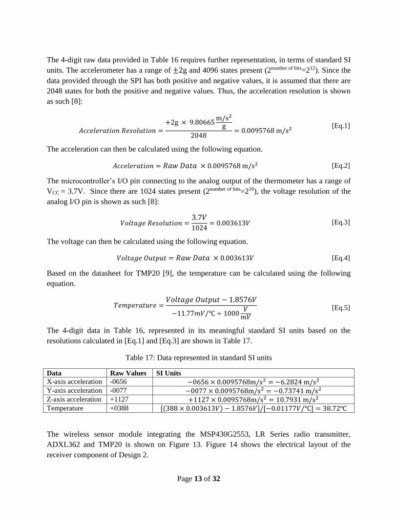
ADXL362 and TMP20 is shown on Figure 13. Figure 14 shows the electrical layout of the
receiver component of Design 2.
Page 14 of 32
Figure 13: Design 2 module physical layout
Figure 14: Design 2 receiver unit
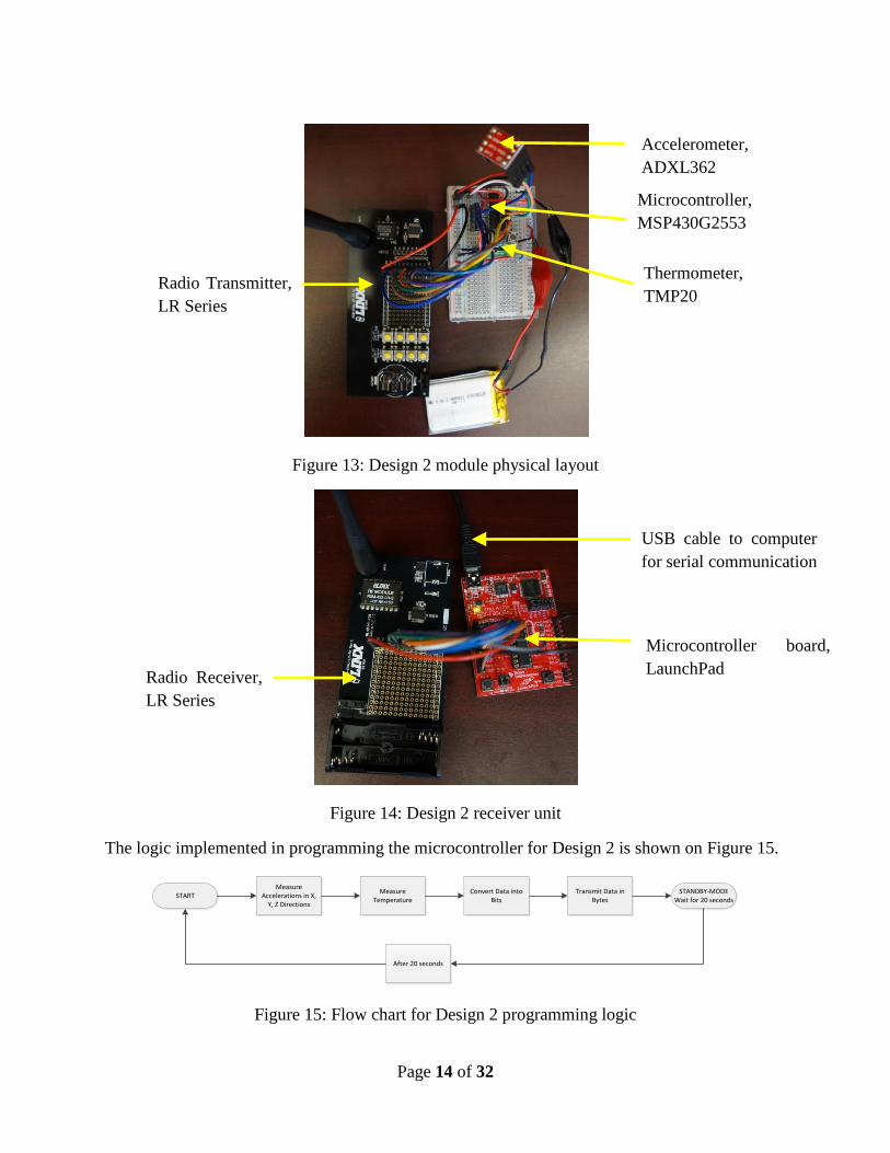
The logic implemented in programming the microcontroller for Design 2 is shown on Figure 15.
Measure Accelerations in X,
Y, Z Directions
Measure Temperature
Convert Data into Bits
STARTSTANDBY-MODE
Wait for 20 seconds
After 20 seconds
Transmit Data in Bytes
Figure 15: Flow chart for Design 2 programming logic
Accelerometer,
ADXL362
Microcontroller,
MSP430G2553
Thermometer,
TMP20 Radio Transmitter,
LR Series
Radio Receiver,
LR Series
USB cable to computer
for serial communication
Microcontroller board,
LaunchPad
Page 15 of 32
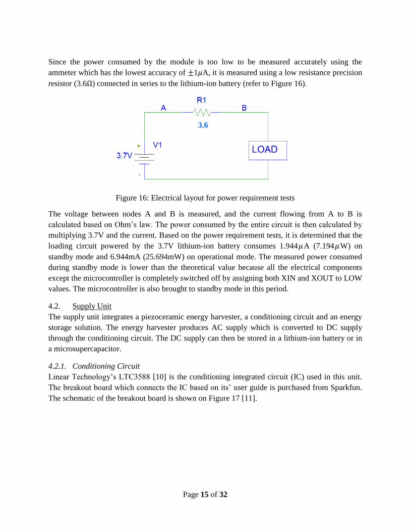
Since the power consumed by the module is too low to be measured accurately using the
ammeter which has the lowest accuracy of ±1𝜇A, it is measured using a low resistance precision
resistor (3.6Ω) connected in series to the lithium-ion battery (refer to Figure 16).
Figure 16: Electrical layout for power requirement tests
The voltage between nodes A and B is measured, and the current flowing from A to B is
calculated based on Ohm’s law. The power consumed by the entire circuit is then calculated by
multiplying 3.7V and the current. Based on the power requirement tests, it is determined that the
loading circuit powered by the 3.7V lithium-ion battery consumes 1.944𝜇A (7.194𝜇W) on
standby mode and 6.944mA (25.694mW) on operational mode. The measured power consumed
during standby mode is lower than the theoretical value because all the electrical components
except the microcontroller is completely switched off by assigning both XIN and XOUT to LOW
values. The microcontroller is also brought to standby mode in this period.
4.2. Supply Unit
The supply unit integrates a piezoceramic energy harvester, a conditioning circuit and an energy
storage solution. The energy harvester produces AC supply which is converted to DC supply
through the conditioning circuit. The DC supply can then be stored in a lithium-ion battery or in
a microsupercapacitor.
4.2.1. Conditioning Circuit
Linear Technology’s LTC3588 [10] is the conditioning integrated circuit (IC) used in this unit.
The breakout board which connects the IC based on its’ user guide is purchased from Sparkfun.
The schematic of the breakout board is shown on Figure 17 [11].
3.6

Page 16 of 32
Figure 17: Schematic of LTC3588 breakout board
LTC3588 integrates a full-wave rectifier which ensures the AC supply from the energy harvester
is converted to a constant positive polarity supply. It also has a under-voltage lockout (UVLO)
circuit which switches on the buck converter when the mean voltage is greater than 5V. The
buck converter then transfers the charge from the input capacitor (C3 in Figure 17) to the output
capacitor (C7 in Figure 17) by alternating the current passing through the inductor (U2 in Figure
17). A comparator is also present in the IC to compare the output voltage and the target voltage
(1.8V, 2.5V, 3.3V, 3.6V). If the output voltage is greater than 92% of the target voltage, pin EN
in Figure 17 will produce a HIGH logic output. The flow chart demonstrating the process carried
out in LTC3588 is shown on Figure 18.
PIEZOFULL-WAVE RECTIFIER
UVLOV_INBUCK CONVERTER
ONIF V_IN > 5V
BUCK CONVERTER OFF
IF V_IN < 5V
CHARGE TRANSFER FROM INPUT
CAPACITOR TO OUTPUT CAPACITOR
IF V_IN > 3.7V
IF V_IN < 3.7VCHARGE
ACCUMULATE IN INPUT CAPACITOR
COMPARE V_OUT AND TARGET
V_OUT
V_OUT
Figure 18: Flow chart demonstrating process in LTC3588
4.2.2. Energy Storage
The DC voltage conditioned by the LTC3588 IC can be stored in a lithium-ion battery or a
microsupercapacitor. In this project, the power generated is used to charge a lithium-ion battery.
Maxim Integrated’s MAX1555 is used as the battery charging IC which directly connects to
Page 17 of 32
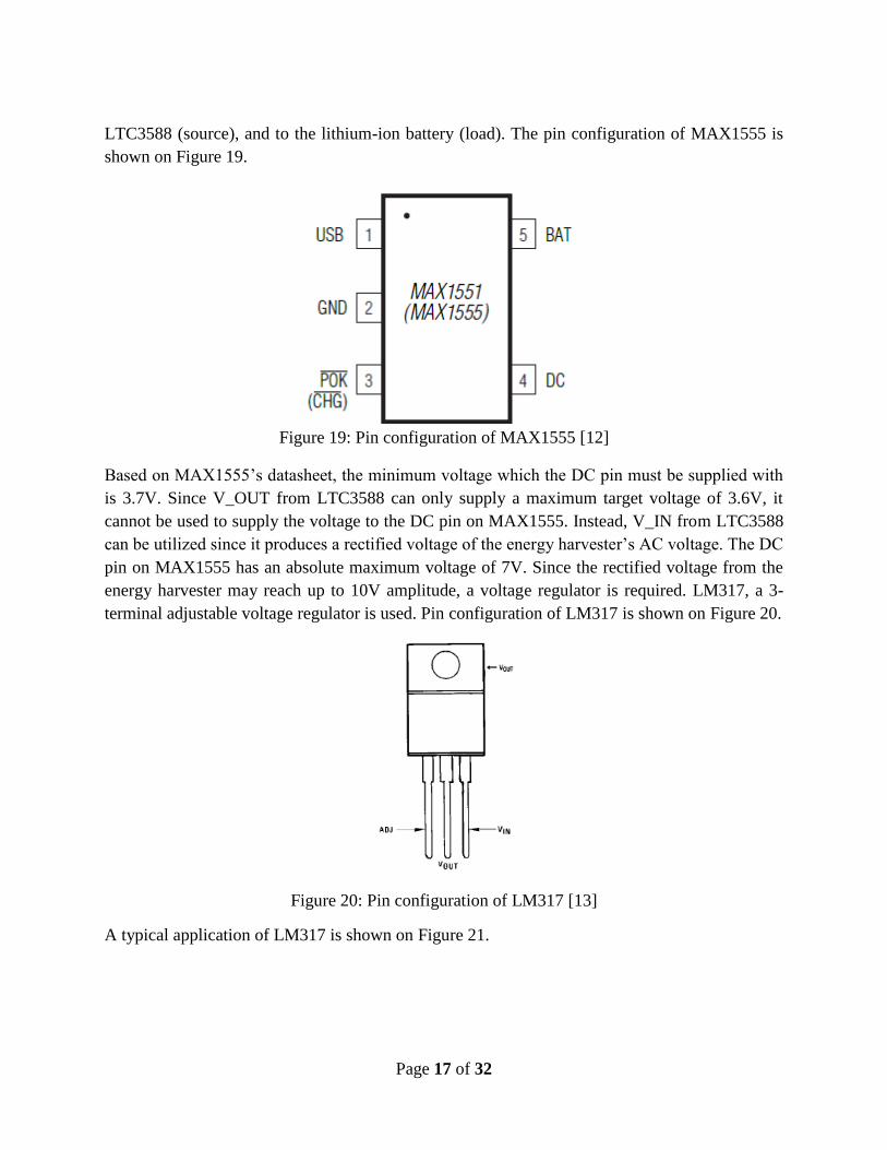
LTC3588 (source), and to the lithium-ion battery (load). The pin configuration of MAX1555 is
shown on Figure 19.
Figure 19: Pin configuration of MAX1555 [12]
Based on MAX1555’s datasheet, the minimum voltage which the DC pin must be supplied with
is 3.7V. Since V_OUT from LTC3588 can only supply a maximum target voltage of 3.6V, it
cannot be used to supply the voltage to the DC pin on MAX1555. Instead, V_IN from LTC3588
can be utilized since it produces a rectified voltage of the energy harvester’s AC voltage. The DC
pin on MAX1555 has an absolute maximum voltage of 7V. Since the rectified voltage from the
energy harvester may reach up to 10V amplitude, a voltage regulator is required. LM317, a 3-
terminal adjustable voltage regulator is used. Pin configuration of LM317 is shown on Figure 20.
Figure 20: Pin configuration of LM317 [13]
A typical application of LM317 is shown on Figure 21.

Page 18 of 32
Figure 21: Typical application of LM317 [14]
Based on LM317’s datasheet, the output voltage can be computed based on the following
equation:
𝑉𝑜𝑢𝑡𝑝𝑢𝑡 = 1.25𝑉 × (1 +𝑅2
𝑅1) [Eq.6]
Since it is required for 𝑉𝑜𝑢𝑡𝑝𝑢𝑡 to be less than 7V, 𝑅1 is chosen to be 4.7kΩ and 𝑅2 is chosen to
be 20k Ω . With this configuration, 𝑉𝑜𝑢𝑡𝑝𝑢𝑡 is regulated to 6.569V. The pin connections on
LTC3588, MAX1555 and LM317 are shown on Table 18.
Table 18: Pin connections on LTC3588, MAX1555, LM317
LTC3588 LM317 MAX1555
PZ1 Piezo + V_IN V_IN (LTC3588) GND GND
PZ2 Piezo - V_ADJ As shown on Figure 21 DC V_OUT (LM317)
GND GND V_OUT DC (MAX1555) BAT V+ (Battery)
V_IN V_IN (LM317)
The breadboard which integrates Design 2 with the energy conditioning and energy storage
circuitry is shown on Figure 22. The piezeoceramic energy harvester is substituted with an AC
source which provides a sinusoidal wave of 10Vpp. The frequency is varied from 10Hz to 1MHz
to determine the effect of frequency on the circuit. Based on the results, frequency does not
significantly affect the circuit’s performance.

Page 19 of 32
Figure 22: Breadboard layout with AC function generator
4.3. PCB Designs
PCBs are designed to miniaturize both the loading unit and the supply unit, and to integrate both
circuits onto a single PCB. The 5 PCBs designed are listed below:
1. WS-Module-rev1.0: Microcontroller and sensors
2. WS-Module-Transmitter: LR Series transmitter and encoder
3. WS-Module-rev1.2: Microcontroller, thermometer, energy harvester conditioning and
energy storage
4. WS-Module-rev1.3: Microcontroller, sensors, energy harvester conditioning and energy
storage
5. WS-Module-rev1.4: Microcontroller, sensors, energy harvester conditioning, energy
storage, and LR Series transmitter and encoder
In order to improve Design 2 (4.1.2), 2 PCBs are designed. The PCB integrating the
microcontroller and sensors is named WS-Module-rev1.0 while the PCB which integrates the LR
series transmitter and encoder is named WS-Module-Transmitter. It is important to note that WS-
Module-rev1.3 integrates all components except the radio module while WS-Module-rev1.4
integrates all the components in both the loading and supply units. The only difference between
AC Function Generator
LR Series Transmitter
Lithium-ion Battery
Breadboard
LED signalling status of
battery charger

Page 20 of 32
WS-Module-rev1.2 and WS-Module-rev1.3 is that WS-Module-rev1.2 is connected externally to
the accelerometer ADXL362 breakout board while WS-Module-rev1.3 has the ADXL362
mounted on it.
4.3.1. WS-Module-rev1.0
Schematic for WS-Module-rev1.0 is shown on Figure 23. Capacitors are added into the design to
reduce power fluctuations in the circuit. A momentary switch is used as a reset button for the
circuit.
Figure 23: Schematics of WS-Module-rev1.0
The board layout of WS-Module-rev1.0 is shown on Figure 24.
Figure 24: Board layout of WS-Module-rev1.0

Page 21 of 32
The WS-Module-rev1.0 PCB populated with the electronics required is shown on Figure 25.
Figure 25: Populated WS-Module-rev1.0 PCB
Electronics are soldered using the hot air reflow technique. The PCB is powered via the GND
and VCC header pins and connected to the radio module via the remaining 10 header pins. After
carrying out some tests (PCB connected to radio module shown on Figure 26), it is determined
that the accelerometer is not functioning on this PCB due to improper soldering technique. The
accelerometer is in a quad-flat no-leads (QFN) package which cannot be soldered through
regular application of solder paste and hot air reflow technique. Bridges are created through this
technique for this particular sensor and cannot be removed using regular solder wick.
Figure 26: WS-Module-rev1.0 connected externally to radio module
Lithium-ion Battery LR Series Transmitter
WS-Module-rev1.0

Page 22 of 32
4.3.2. WS-Module-Transmitter
Schematic for WS-Module-Transmitter is shown on Figure 27. The circuit is designed based on
the application notes and user guides provided by the manufacturer, Linx Technologies [15].
Jumper wires will be connected from the header pins on WS-Module to the header pins on WS-
Module-Transmitter. The board layout of WS-Module-Transmitter is shown on Figure 28.
Figure 27: Schematics of WS-Module-Transmitter

Page 23 of 32
Figure 28: Board layout of WS-Module-Transmitter
In order to improve the radio transmission of data, high power transfer efficiency from the source
(LR series transmitter module) to the load (radio antenna) must be achieved. This can be done
through impedance matching, i.e., the impedance at the loading unit must be equal to the
impedance at the source unit for maximum power transfer. Since the radio antenna has an
impedance of 50Ω, the trace from the radio transmitter to the SMA connector (which directly
connects to the antenna) must also have an impedance of 50Ω. Figure 29 shows the location of a
trace on a standard PCB and the values of variables provided by the PCB manufacturer [16].
W Trace width [mm] 3.21mm
T Trace thickness [mm] 0.035mm
H Dielectric thickness [mm] 1.6mm
𝜀𝑟 Relative permittivity 3.7
Figure 29: Trace on a PCB [17]
Using the following formula [18], the trace width required to obtain the 50Ω impedance is
3.21mm.
𝑍𝑜[𝛺] =87
√𝜀𝑟 + 1.41𝑙𝑛
5.98𝐻
0.8𝑊 + 𝑇 [Eq.7]

Page 24 of 32
Electronics are soldered onto the PCB using the hot air reflow technique. The PCB is connected
to WS-Module-rev10 via header pins. The populated WS-Module-Transmitter PCB connected to
the WS-Module-rev10 is shown on Figure 30. After carrying out some tests, it is determined that
the transmitter PCB is not functioning. It is deduced that it may be due to incorrect trace width
design.
Figure 30: Populated WS-Module Transmitter connected to WS-Module-rev1.0
4.3.3. WS-Module-rev1.2
WS-Module-rev1.2 integrates the microcontroller, thermometer, energy conditioning and energy
storage circuitry. The accelerometer ADXL362 breakout board and radio module are then
connected externally to this PCB. Schematic of this design is shown in Figure 31.
WS-Module Transmitter
Lithium-ion Battery
WS-Module-rev1.0

Page 25 of 32
Figure 31: Schematics of WS-Module-rev1.2
The board layout is shown in Figure 32.
Figure 32: Board layout of WS-Module-rev1.2
Page 26 of 32
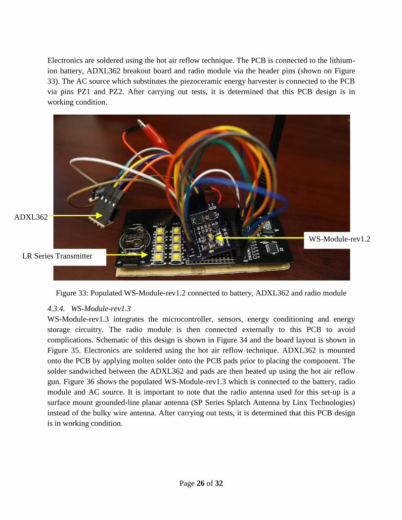
Electronics are soldered using the hot air reflow technique. The PCB is connected to the lithium-
ion battery, ADXL362 breakout board and radio module via the header pins (shown on Figure
33). The AC source which substitutes the piezoceramic energy harvester is connected to the PCB
via pins PZ1 and PZ2. After carrying out tests, it is determined that this PCB design is in
working condition.
Figure 33: Populated WS-Module-rev1.2 connected to battery, ADXL362 and radio module
4.3.4. WS-Module-rev1.3
WS-Module-rev1.3 integrates the microcontroller, sensors, energy conditioning and energy
storage circuitry. The radio module is then connected externally to this PCB to avoid
complications. Schematic of this design is shown in Figure 34 and the board layout is shown in
Figure 35. Electronics are soldered using the hot air reflow technique. ADXL362 is mounted
onto the PCB by applying molten solder onto the PCB pads prior to placing the component. The
solder sandwiched between the ADXL362 and pads are then heated up using the hot air reflow
gun. Figure 36 shows the populated WS-Module-rev1.3 which is connected to the battery, radio
module and AC source. It is important to note that the radio antenna used for this set-up is a
surface mount grounded-line planar antenna (SP Series Splatch Antenna by Linx Technologies)
instead of the bulky wire antenna. After carrying out tests, it is determined that this PCB design
is in working condition.
LR Series Transmitter
ADXL362
WS-Module-rev1.2

Page 27 of 32
Figure 34: Schematics of WS-Module-rev1.3
Figure 35: Board layout of WS-Module-rev1.3

Page 28 of 32
Figure 36: Populated WS-Module-rev1.3 connected to battery, radio module and AC source
LR Series Transmitter Surface Mount Antenna
WS-Module-rev1.3
AC Function Generator
LED signalling status of
battery charger

Page 29 of 32
4.3.5. WS-Module-rev1.4
WS-Module-rev1.4 integrates all the components in this design: microcontroller, sensors, radio
module, energy conditioning and energy storage circuitry. The PCB is powered externally
through a lithium-ion battery. Schematic of this design is shown in Figure 37 while the board
layout is shown in Figure 38. Since this PCB was designed based on WS-Module Transmitter, it
can be deduced that this design will not be functional due to the flaws in WS-Module
Transmitter. However, this design demonstrates that this concept can be realized into a 50mm ×
35mm PCB.
5. Summary and Future Work
In summary, a self-powered wireless sensor module is an idea which can be developed into
reality. In this project, a microcontroller (MSP430G2553), a thermometer (TMP20), an
accelerometer (ADXL362), a 433MHz radio transmitter (LR Series) and a PCB antenna (SP
Series) are integrated into a 50mm × 35mm PCB. The circuit consumes 7.194𝜇W on standby
mode and 25.694mW on operational mode. This can be sustained by the current state-of-the-art
piezoceramic energy harvester which is capable of generating 100𝜇W from a body vibrating at a
constant 1g or 9.81m/s2 acceleration. This project serves as a proof of concept, and can be
modified accordingly to requirements by using different electronic components.
If future work is to be carried out to this design, impedance matching to allow data transmission
must be carried out, through proper PCB trace design. Range of data transmission should be
tested to ensure it meets the theoretical 1km range. Packaging of the wireless sensor module
must also be taken into account, and should be tested for robustness.

Page 30 of 32
Figure 37: Schematics of WS-Module-rev1.4

Page 31 of 32
Figure 38: Board layout of WS-Module-rev1.4

Page 32 of 32
6. References
[1] Arduino, "Arduino Uno," 2013. [Online]. Available:
http://arduino.cc/en/Main/arduinoBoardUno. [Accessed 1 May 2013].
[2] Arduino, "Arduino Fio," 2013. [Online]. Available:
http://arduino.cc/en/Main/ArduinoBoardFio. [Accessed 1 May 2013].
[3] Sparkfun Electronics, "Infrared Thermometer - MLX90614," 2013. [Online]. Available:
https://www.sparkfun.com/products/9570. [Accessed 15 May 2013].
[4] Sparkfun Electronics, "Pulse Sensor," 2013. [Online]. Available:
https://www.sparkfun.com/products/11574. [Accessed 15 May 2013].
[5] Texas Instruments, "MSP430 LaunchPad Value Line Development Kit," 2013. [Online].
Available: http://www.ti.com/tool/msp-exp430g2#0. [Accessed 1 June 2013].
[6] Sparkfun Electronics, "Triple Axis Accelerometer Breakout - ADXL362," 2013. [Online].
Available: https://www.sparkfun.com/products/11446. [Accessed 10 June 2013].
[7] Mouser Electronics, "Linx Technologies EVAL-433-LR," 2013. [Online]. Available:
http://ca.mouser.com/ProductDetail/Linx-Technologies/EVAL-433-
LR/?qs=K5ta8V%252bWhtZQ8bzSTCQmsg==. [Accessed 10 June 2013].
[8] R. Ben Mrad, Quantization Theory, A/D and D/A Conversions, Toronto, 2013.
[9] Texas Instrument, "Application Information," Temperature Sensor (TMP20), vol. SBOS466,
December, 2009.
[10] Linear Technology, "LTC3588 - Piezoelectric Energy Harvesting Power Supply," 2013.
[Online]. Available: http://www.linear.com/product/LTC3588-1. [Accessed 25 July 2013].
[11] Sparkfun Electronics, "Energy Harvester - LTC3588 Breakout," 2013. [Online]. Available:
https://www.sparkfun.com/products/9946. [Accessed 10 July 2013].
[12] Maxim Integrated, "MAX1551/MAX1555," 19-2902, 2003.
[13] Electronics Lab, "LM317 Calculator," 2013. [Online]. Available: http://www.electronics-
lab.com/articles/LM317/. [Accessed 1 August 2013].
[14] Fairchild Semiconductor, "LM317: 3-Terminal Positive Adjustable Regulator," 2013.
[15] Linx Technologies, "LR Series Basic Evaluation Kit," 2012. [Online]. Available:
https://www.linxtechnologies.com/resources/data-guides/eval-xxx-lr.pdf. [Accessed 1 July
2013].
[16] OSH Park, "Pricing and Specifications," 2013. [Online]. Available:
http://oshpark.com/pricing. [Accessed 22 July 2013].
[17] Missouri University of Science and Technology, "Microstrip Impedance Calculator," 2008.
[Online]. Available: http://emclab.mst.edu/pcbtlc2/microstrip/. [Accessed 23 July 2013].
[18] Institute for Interconnecting and Packaging Electronic Circuits (Northbrook, Ill.), Institute
for Interconnecting and Packaging Electronic Circuits (Evanston, Ill.). High Speed/High
Frequency Committee. IPC-D-317 Task Group, Design Guidelines for Electronic Packaging
Utilizing High-speed Techniques, IPC, 1995.