Embed Size (px)
Citation preview
—
'
-
’
-
-
-
’
- -
“ ”-
-
- --
--
-
-
--
-
--
-
—
-
’
-
’-
-
-
Seeing Matter at Atomic and Molecular Scales From Nanoscale Structure to Macroscale Properties
Studying matter at the level of atoms and molecules requires measuring structures that are billionths of a meter (nanometers) or less in size. This nanoscale realm is where the fundamental properties of materials
are established. Melting temperature, magnetic properties, charge capacity, and even color are dictated by the arrangements of atoms and molecules. The ability to understand, design, and control these properties will lead to a new world of materials and technologies for numerous application areas.
An atom s typical size is tenths of a nanometer. The wavelength range of visible light is a few hundred nanometers, which is too large to detect atoms. Seeing matter at the level of atoms requires instruments that can measure structures that are one thousand times smaller than those detectable by the most advanced light microscopes. Thus, to characterize structures with atomic detail, we must use probes such as x-rays, electrons, and neutrons that are at least as small as the atoms being investigated.
X-Ray Science For nearly a century, x-ray beams have been our principal means of unraveling the identities and positions of atoms in crystallized samples ranging from relatively simple metal materials to highly complex biological molecules like proteins and DNA. Due to their short wave length, hard x-rays are very useful for probing atomic structure. Today s synchrotron radiation and free electron laser light sources produce x-rays so intense that they have vastly eclipsed historical methods and have given rise to scores of new ways to do experiments.
Crystallized samples of materials are analyzed by passing x-rays through them. The x-rays are scattered by the atoms of a crystal, producing a difraction image on detectors. This image
By understanding the atom by atom assembly of provides unique information on the identity of the atoms and structure of the crystal. Large, fexible materials into stable confgurations, researchers membrane proteins, such as Photosystem I in plant cells, form very small crystals that tend to be are gaining new insights into improving existing imperfect and weakly difracting. Intense x-ray sources have been invaluable for determining the materials and synthesizing new nanostructures with structures and properties of such macromolecules. superior strength, durability, corrosion resistance, and other desired properties.
How do only 118 building blocks—all the known elements in the periodic table combine to create every substance on Earth? How do these atoms make materials with a seemingly endless variety of forms and properties—soft and hard, ductile and brittle, magnetic and nonmagnetic, insulating and superconducting, living and nonliving? Why do the same atoms connected in varying ways yield remarkably diferent materials? Finding out is key to creating the materials and technologies needed to thrive in an age of natural resource, environ mental, and fscal constraints. This quest begins with visualizing atoms (nuclei and electrons) and their interactions.
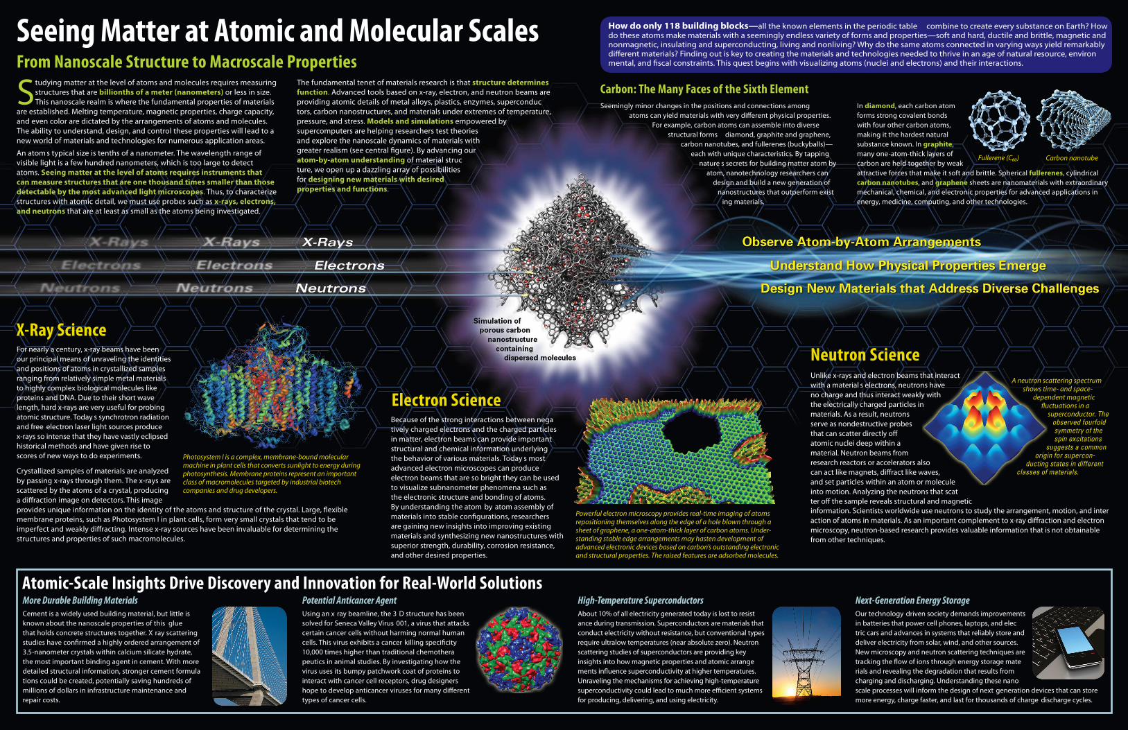
Carbon: The Many Faces of the Sixth Element Seemingly minor changes in the positions and connections among
atoms can yield materials with very diferent physical properties. For example, carbon atoms can assemble into diverse
structural forms diamond, graphite and graphene, carbon nanotubes, and fullerenes (buckyballs)—
each with unique characteristics. By tapping nature s secrets for building matter atom by
atom, nanotechnology researchers can design and build a new generation of
nanostructures that outperform exist ing materials.
In diamond, each carbon atom forms strong covalent bonds with four other carbon atoms, making it the hardest natural substance known. In graphite, many one-atom-thick layers of Fullerene (C₆₀) Carbon nanotube carbon are held together by weak attractive forces that make it soft and brittle. Spherical fullerenes, cylindrical carbon nanotubes, and graphene sheets are nanomaterials with extraordinary mechanical, chemical, and electronic properties for advanced applications in energy, medicine, computing, and other technologies.
Photosystem I is a complex, membrane-bound molecular machine in plant cells that converts sunlight to energy during photosynthesis. Membrane proteins represent an important class of macromolecules targeted by industrial biotech companies and drug developers.
The fundamental tenet of materials research is that structure determines function. Advanced tools based on x-ray, electron, and neutron beams are providing atomic details of metal alloys, plastics, enzymes, superconduc tors, carbon nanostructures, and materials under extremes of temperature, pressure, and stress. Models and simulations empowered by supercomputers are helping researchers test theories and explore the nanoscale dynamics of materials with greater realism (see central fgure). By advancing our atom-by-atom understanding of material struc ture, we open up a dazzling array of possibilities for designing new materials with desired properties and functions.
Electron Science Because of the strong interactions between nega tively charged electrons and the charged particles in matter, electron beams can provide important structural and chemical information underlying the behavior of various materials. Today s most advanced electron microscopes can produce electron beams that are so bright they can be used to visualize subnanometer phenomena such as the electronic structure and bonding of atoms.
Neutron Science
origin for supercon-suggests a common
dependent magnetic the electrically charged particles in fuctuations in a materials. As a result, neutrons superconductor. The serve as nondestructive probes observed fourfold
symmetry of the
research reactors or accelerators also can act like magnets, difract like waves, and set particles within an atom or molecule into motion. Analyzing the neutrons that scat ter of the sample reveals structural and magnetic information. Scientists worldwide use neutrons to study the arrangement, motion, and inter action of atoms in materials. As an important complement to x-ray difraction and electron microscopy, neutron-based research provides valuable information that is not obtainable from other techniques.
with a material s electrons, neutrons have Unlike x-rays and electron beams that interact
A neutron scattering spectrum shows time- and space-
ducting states in different classes of materials.
no charge and thus interact weakly with
that can scatter directly of spin excitationsatomic nuclei deep within a
material. Neutron beams from
Powerful electron microscopy provides real-time imaging of atoms repositioning themselves along the edge of a hole blown through a sheet of graphene, a one-atom-thick layer of carbon atoms. Under-standing stable edge arrangements may hasten development of advanced electronic devices based on carbon’s outstanding electronic and structural properties. The raised features are adsorbed molecules.
Atomic-Scale Insights Drive Discovery and Innovation for Real-World Solutions More Durable Building Materials Potential Anticancer Agent High-Temperature Superconductors Next-Generation Energy Storage Cement is a widely used building material, but little is Using an x ray beamline, the 3 D structure has been About 10% of all electricity generated today is lost to resist Our technology driven society demands improvements known about the nanoscale properties of this glue solved for Seneca Valley Virus 001, a virus that attacks ance during transmission. Superconductors are materials that in batteries that power cell phones, laptops, and elec that holds concrete structures together. X ray scattering certain cancer cells without harming normal human conduct electricity without resistance, but conventional types tric cars and advances in systems that reliably store and studies have confrmed a highly ordered arrangement of cells. This virus exhibits a cancer killing specifcity require ultralow temperatures (near absolute zero). Neutron deliver electricity from solar, wind, and other sources. 3.5-nanometer crystals within calcium silicate hydrate, 10,000 times higher than traditional chemothera scattering studies of superconductors are providing key New microscopy and neutron scattering techniques are the most important binding agent in cement. With more peutics in animal studies. By investigating how the insights into how magnetic properties and atomic arrange tracking the fow of ions through energy storage mate detailed structural information, stronger cement formula virus uses its bumpy patchwork coat of proteins to ments infuence superconductivity at higher temperatures. rials and revealing the degradation that results from tions could be created, potentially saving hundreds of interact with cancer cell receptors, drug designers Unraveling the mechanisms for achieving high-temperature charging and discharging. Understanding these nano millions of dollars in infrastructure maintenance and hope to develop anticancer viruses for many diferent superconductivity could lead to much more efcient systems scale processes will inform the design of next generation devices that can store repair costs. types of cancer cells. for producing, delivering, and using electricity. more energy, charge faster, and last for thousands of charge discharge cycles.

User Facilities: Tools for Seeing Atoms Revealing the atomic-scale secrets of materials requires a variety of cutting-edge imaging and analytical instru-
ments that use beams of diferent types of particles or radiation. These beams of x-rays, neutrons, and electrons provide complementary information about various aspects of a material’s nanoscale structure. These techniques
together are revealing insights that enable us to understand and ultimately control the properties of materials.
Building on investments made by the Department of Energy (DOE) and its predecessor agencies in pioneering work to develop nuclear reactors and particle accelerators, the DOE Ofce of Science today provides the research community with a suite of scientifc user facilities—x-ray light sources, neutron sources, and electron-beam micro-characterization centers—to explore the atomic world. Since their inception in the 1970s, the growth of scientifc user facilities worldwide has been remarkable. Major scientifc user facilities make possible experimental studies that cannot be done in ordinary laboratories, and these facilities have created a new style of research in which scientists conduct investigations that beneft from a merging of ideas and techniques from diferent disciplines.
Together, these DOE facilities help more than 10,000 researchers pursue discoveries that improve the economy, energy options, medical treatments, technologies, and our fundamental understanding of the materials that make up our world. The leading-edge research conducted at these facilities has earned numerous awards, including Nobel prizes in chemistry, physics, and medicine. Selected facilities are described below.
X-Ray Light Sources Millions of times brighter than medical x-rays, light sources generate high-quality, stable beams of x-rays and other elec-tromagnetic radiation that can be used for numerous experi-mental techniques. Electrons are defected as they travel past bending magnets along the circular track of a synchrotron or through other specially designed magnetic devices. This creates a continuous spectrum of radia-tion with various wavelengths and strengths (e.g., ultraviolet light and hard or soft x-rays) that scientists can select to suit their particular experiment. These rays are then sent down pipes called beamlines to sophisticated instruments in work areas or end stations where studies are conducted.
The Advanced Photon Source (APS) is the largest scientifc user facility in the United States (its electron storage ring could encircle a major-league baseball stadium). By bending accelerated electrons into a circular path with magnetic felds, the APS produces ultrabright radiation in the hard x-ray range that can be focused onto small samples, allowing researchers to quickly gather large amounts of detailed data. With over 60 beamlines equipped with numerous instruments customized to particular research needs, the APS ofers a broad range of experimental capabilities.
The Linac Coherent Light Source (LCLS) is an x-ray free-electron laser that is used much like a super high-speed strobe fash that produces very short pulses of electrons. The LCLS electron beam is linear, and the electrons travel through a 1-kilometer-long accelerator before emitting x-rays as they slalom back and forth within the fnal 100-meter stretch of undulators. The waves of x-rays become synchronized as they further interact with the electron pulses. The resulting ultrafast pulses of hard x-rays allow scientists to take stop-motion pictures of moving molecules, shedding light on the fundamental processes of chemistry, technology, and life itself.
Each 2-m-long, 1-ton undulator at LCLS contains many “teeth,” or alternating pairs of north-south magnets that force electrons to follow a wavy path, creating x-rays.
Measurement Techniques for Instruments Using X-Ray, Electron, and Neutron Beams Imaging Imaging techniques use particle beams to obtain pictures with fne spatial resolution of materials. Microscopy using electrons or x-rays is now powerful enough to image individual atoms within a structure, reveal local physical properties by measuring Arrangement small shifts in the positions of atoms, and of atoms in study molecular events that last only one an aluminum millionth of a billionth of a second. alloy.
Scattering Scattering or difraction occurs when a stream of particles or a wave strikes an object and is defected from its original trajectory. When a particle beam is aimed at a sample, some of these particles will interact with nuclei or with X-ray the electrons surrounding nuclei and bounce diffraction away at an angle. The scattering pattern created of a single when the “bounced” particles hit a detector gives virus information about the structure of the sample. particle.
Neutron Sources Neutrons are produced for scientifc experiments in a reactor or using an accelerator-based process called spallation. By bombarding a heavy-element target (e.g., mercury) with accelerated protons, spallation causes some neutrons to be knocked out or “boiled of” as the bombarded nuclei heat up. When the energetic protons collide with the heavy atomic nuclei in the target, about 20 to 30 neutrons are expelled from each nucleus.
Neutrons from these sources are guided through beamlines to the sample material being investigated. The neutrons bounce of the sample, scattering in diferent directions. Where they bounce, how fast, and where they land reveal details about the sample’s properties. Special detectors measure these scattering patterns and send the data to a computer for various analyses and processing, which often include reconstructing a three-dimensional image of a sample’s nanoscale archi-tecture. Such images provide unique insights into a material’s structure, dynamics, and magnetic properties.
The Spallation Neutron Source (SNS) is a pulsed accelerator-based neu-tron source. Before hitting a target, protons are accelerated to very high energies and passed into a ring where they accumulate in bunches. Each bunch is released from the ring as a pulse, creating a neutron beam 10 times more intense than any other such source in the world. Each pulse contains neutrons in a range of wavelengths and energies tuned to a specifc experiment by moder-ators. The highest energy neutrons are moderated to room temperature or cooler. Cooling neutrons slows their speed and lengthens their wavelengths to levels suitable for analyzing certain magnetic properties or studying the larger structural components of “soft” materials such as proteins and polymers.
The SNS chamber contains the central liquid mercury target that is bombarded by protons to produce spallation neutrons.
Electron-Beam Microcharacterization More than a thousand times smaller than neutrons, electrons are tiny, negatively charged particles that can be energized, defected, or focused into beams by electric and magnetic felds. Electrons interact so strongly with the nuclei and electrons of atoms that they scatter with much higher intensity than x-rays or neutrons, thereby generating powerful signals from small numbers of atoms and even from just a single atom. These attributes make electrons very useful not only for characterizing matter at subnanometer to micrometer scales but also for capturing images of individual atoms within a sample.
The National Center for Electron Microscopy (NCEM) at Lawrence Berkeley National Laboratory is home to the Transmission Electron Aberration-corrected Microscope (TEAM). TEAM is the product of a collaboration among DOE electron-beam experts to develop the frst electron microscope to surpass a spatial resolution of 0.05 nanometers, roughly half the diameter of a hydrogen atom.
TEAM is the world’s most powerful electron microscope.
An electron gun atop the TEAM instrument applies an intense electrical feld and heat to emit electrons from a source material. The electron gun accelerates and focuses the emitted electrons into a tight beam traveling at more than half the speed of light. The accelerated electrons behave like waves with very short wave-lengths. Once shot from the electron gun, the beam is condensed and directed toward the sample. The electron waves zoom through the sample and into a series of magnetic lenses that magnify and focus them to form an image on a screen at the bottom of the microscope column. As they pass through the magnetic lenses, some electron waves are bent at diferent angles, blurring the image. TEAM components correct these aberrations, giving this instrument its unprecedented capability of directly imaging subatomic distances with ultrahigh precision.
Scientifc User Facilities U.S. Department of Energy, Ofce of Science Ofce of Basic Energy Sciences
X-Ray Light Sources National Synchrotron Light Source (NSLS) Brookhaven National Laboratory, Upton, New York
Stanford Synchrotron Radiation Lightsource (SSRL) SLAC National Accelerator Laboratory, Menlo Park, California
Advanced Light Source (ALS) Lawrence Berkeley National Laboratory, Berkeley, California
Advanced Photon Source (APS) Argonne National Laboratory, Argonne, Illinois
Linac Coherent Light Source (LCLS) SLAC National Accelerator Laboratory, Menlo Park, California
Aerial view of the Advanced Photon Source
Neutron Scattering Facilities Spallation Neutron Source (SNS) Oak Ridge National Laboratory, Oak Ridge, Tennessee
High Flux Isotope Reactor (HFIR) Oak Ridge National Laboratory, Oak Ridge, Tennessee
Manuel Lujan Jr. Neutron Scattering Center (Lujan Center) Los Alamos National Laboratory, Los Alamos, New Mexico
Aerial view of the Spallation Neutron Source
Electron-Beam Microcharacterization Centers Electron Microscopy Center (EMC) Argonne National Laboratory, Argonne, Illinois
National Center for Electron Microscopy (NCEM) Lawrence Berkeley National Laboratory, Berkeley, California
Shared Research Equipment (SHaRE) User Facility Oak Ridge National Laboratory, Oak Ridge, Tennessee
Ofce of Basic Energy Sciences science.energy.gov/bes/suf/user-facilities/
Image credits. Fullerene and nanotube: Laguna Design/Photo Researchers. Carbon nanostructure, neutron scattering spectrum, scale of subvisible world, SNS chamber, and aerial of Spallation Neutron Source: Oak Ridge National Laboratory. Photosystem I: Protein Data Bank (www.rcsb.org) PDB ID 3PCQ visualized using iMol. Hole in sheet of carbon atoms, TEAM instrument, and micrograph of atoms in alloy: Lawrence Berkeley National Laboratory. Bridge, powerline, and electronic devices: iStockphoto. Undulator: Linac Coherent Light Source, SLAC National Accelerator Laboratory. X-ray difraction of virus: T. Ekeberg, Uppsala University. Seneca Valley Virus, orbitals in metal oxide, and aerial of Advanced Photon Source: Argonne National Laboratory.
May 2011
Spectroscopy Spectroscopy is the study of the interac-tions between matter and radiated energy. The spectrum of wavelengths or frequen-cies of energies absorbed or emitted by the sample under investigation contains information about the electronic struc-ture of the matter, such as the nature of its chemical bonds or the behavior of its electrons during excitation.
Electron orbital positioning of a metal oxide interface revealed by x-ray spectroscopy.


![HANGING SCALES/CRANE SCALES - Aviga HFO 159 page 166 1020,-from € Hanging scales/Crane scales Lisa Mayer Product specialist Hanging scales/Crane scales Tel. +49 [0] 7433 9933 - 219](https://img.pdfslide.us/doc/110x75/5afd22507f8b9a68498c727e/hanging-scalescrane-scales-hfo-159-page-166-1020-from-hanging-scalescrane.jpg)