Embed Size (px)
Citation preview
Security assessment for automotive
controllers using side channel and
fault injection attacks
A Master’s ThesisSubmitted to the Faculty of the
Escola Tecnica d’Enginyeria de Telecomunicacio deBarcelona
Universitat Politecnica de Catalunyaby
Santiago Cordoba Pellicer
In partial fulfilmentof the requirements for the degree of
MASTER IN ELECTRONIC ENGINEERING
Advisor: Francesc Moll Echeto
Barcelona, February 2018
Title of the thesis: Security assessment for automotive controllers usingside channel and fault injection attacks
Author: Santiago Cordoba Pellicer
Advisor: Francesc Moll Echeto
Abstract
Embedded security is nowadays a hot topic. With the arrival of Inter-net of Things and the increasing demand of connectivity for embedded sys-tems in many industrial markets, including automotive systems, securityhas become an important factor in product design. This thesis is aimedto test the security capabilities of automotive electronic devices, usingphysical attacks known as fault injection. Although other industries havebeen using countermeasures against physical attacks for decades, theseare rarely used in automotive embedded systems. Automotive industryefforts have been focused in improving safety and reliability (e.g. ISO26262 ASIL certification) instead of security. Previous research provedthe risk of fault injection attacks on automotive SoCs, but these workswere limited to small testing applications running on evaluation boardsand not real automotive systems. The current work aims to assess the se-curity of off-the-shelf automotive systems running real applications. Morespecifically, fault injection attacks are used to bypass the authenticationmechanism of the Unified Diagnostic System (ISO 14229) present in twodifferent commercial car dashboards. The findings are exposed in orderto suggest design improvements and recommendations for a more secureautomotive embedded systems and SoCs.
Keywords - Fault Injection; Automotive; ECU; UDS; ISO14229
1
Para todos aquellos que me han acompanado en este viaje:
a mi familia, desde siempre y hasta siempre;a mis amigos, a quienes la distanca nunca ha importado;
y a los errantes y nomadas de este mundo, esten donde esten.
S.
Contents
1 Introduction 41.1 Motivation and Objectives . . . . . . . . . . . . . . . . . . . . . . 51.2 About Riscure BV . . . . . . . . . . . . . . . . . . . . . . . . . . 5
2 State of the Art 82.1 Side Channels . . . . . . . . . . . . . . . . . . . . . . . . . . . . . 82.2 Fault Injection Techniques . . . . . . . . . . . . . . . . . . . . . . 9
2.2.1 Clock Glitching . . . . . . . . . . . . . . . . . . . . . . . . 92.2.2 Voltage Glitching . . . . . . . . . . . . . . . . . . . . . . . 102.2.3 Electromagnetic Fault Injection . . . . . . . . . . . . . . . 112.2.4 Optical Fault Injection . . . . . . . . . . . . . . . . . . . . 14
2.3 Effects of Fault Injection . . . . . . . . . . . . . . . . . . . . . . . 152.3.1 Fault Models . . . . . . . . . . . . . . . . . . . . . . . . . 16
3 Methodology 193.1 Objectives . . . . . . . . . . . . . . . . . . . . . . . . . . . . . . . 193.2 Targets . . . . . . . . . . . . . . . . . . . . . . . . . . . . . . . . 193.3 Fault injection setup . . . . . . . . . . . . . . . . . . . . . . . . . 203.4 Perturbation parameters . . . . . . . . . . . . . . . . . . . . . . . 223.5 Experimental setup . . . . . . . . . . . . . . . . . . . . . . . . . . 22
3.5.1 ECU1 . . . . . . . . . . . . . . . . . . . . . . . . . . . . . 233.5.2 ECU2 . . . . . . . . . . . . . . . . . . . . . . . . . . . . . 26
3.6 Characterization . . . . . . . . . . . . . . . . . . . . . . . . . . . 283.6.1 Diagnostic Services . . . . . . . . . . . . . . . . . . . . . . 283.6.2 FI characterization . . . . . . . . . . . . . . . . . . . . . . 313.6.3 ECU1 . . . . . . . . . . . . . . . . . . . . . . . . . . . . . 333.6.4 ECU2 . . . . . . . . . . . . . . . . . . . . . . . . . . . . . 35
4 Results 444.1 ECU1 . . . . . . . . . . . . . . . . . . . . . . . . . . . . . . . . . 444.2 ECU2 . . . . . . . . . . . . . . . . . . . . . . . . . . . . . . . . . 45
5 Conclusions and Future Work 465.1 Countermeasures . . . . . . . . . . . . . . . . . . . . . . . . . . . 46
5.1.1 Hardware . . . . . . . . . . . . . . . . . . . . . . . . . . . 465.1.2 Software . . . . . . . . . . . . . . . . . . . . . . . . . . . . 47
5.2 Future work . . . . . . . . . . . . . . . . . . . . . . . . . . . . . . 47
A ISO 14229: Unified Diagnostic Services (UDS) 49A.1 DiagnosticSessionControl . . . . . . . . . . . . . . . . . . . . . . 49A.2 ReadMemoryByAddress . . . . . . . . . . . . . . . . . . . . . . . 50A.3 SecurityAccess . . . . . . . . . . . . . . . . . . . . . . . . . . . . 50
B Listings 54
Acronyms 60
References 61
3
1 Introduction
Vehicles have changed considerably in the last decades. Automotive design isabandoning traditional mechanical solutions for newer electronic based solu-tions. Modern cars include all type of electronic systems implementing a widevariety of functionalities, from switching lights to control the injection of fuel inthe engine. These electronic systems have great advantages and they make pos-sible to design more efficient, more comfortable and safer cars. With a notableincrease in the number of electronic controllers in vehicles, electronic design isnowadays an important stage on automotive industry.
Electronic design has many aspects to consider in its work-flow. Every designhas a certain purpose in mind, usually in terms of performance, power savingand cost. In industrial and some consumer designs, reliability is a critical aspectto consider. Reliability is specially important when a malfunction on the designmay lead to a dangerous and harmful situation. It is not hard to see why anautomotive design would have strict reliability requirements: malfunctions in acritical electronic system of a car can put in risk the car passengers and otherpeople in the car surroundings.
Along with the reliability requirements, there is another aspect in electronicdesign that is less known and not frequently considered: security. Designs withsecurity in scope have protection from undesired modifications and accessesthat may as well lead to a undesired or dangerous situation. A poor securityautomotive electronic design may be exposed to attacks that may lead to severeconsequences:
• Firmware extraction: this implies the extraction of the program runningin the digital system, which may contain proprietary technologies, an im-portant asset for manufacturers, leading to industrial espionage and unfaircompetitive edge. The analysis of the extracted firmware can reveal alsoexploitable vulnerabilities that the attacker may use to compromise thesystem in a different way. For example, a vulnerability found in a cryp-tographic function from the system, discovered using firmware extractionand analysis, could lead to an exploit that would allow an attacker tounlock the doors of the car without the genuine keys.
• Firmware modification: after a firmware extraction attackers could makea firmware modifications. Applying patches to the firmware of a automo-tive electronic controller is one of the objective of a car tuner attacker,motivated by a possible increase of performance in the vehicle by alteringthe software. These modifications are a great risk to the integrity of thecar and could potentially lead to accidents. Furthermore, it is possible tomodify the software of a car controller intentionally and inflict damage tothe vehicle and its occupants by the means of sabotage.
• Runtime control and access to debug interfaces: these are usually inter-mediate steps in the way to the previously mentioned situations. Hav-ing runtime control and access to debug interfaces could also help in thefirmware download, analysis and modification. Having a running target
4

is very helpful in order to reverse engineer a firmware image, and also todevelop patches and modifications.
Along with this scenarios, other security related issues may happen. Anexample of this is the violation of passenger’s privacy, as an attacker could com-promise the convenience system in which the hands-free phone call system isbuilt in, listening to the phone calls made or answered from the car, or evenlistening what the car microphone is recording. Moreover, an attacker couldtarget the GPS navigation system and track a given vehicle, gathering preciousinformation about the passengers’ location.
1.1 Motivation and Objectives
The objective of the present work is to assess the security of automotive sys-tems using fault injection (FI) techniques. Academic research regarding faultinjection in automotive systems with security implications in scope is almostnonexistent. Previous work regarding security in automotive hardware makeuse of FI to unlock access to debug interfaces [1] and then compromise thesystem. Nevertheless, these experiments are performed under laboratory con-ditions, commonly using a development board as targets, whereas the presentwork uses commercially available electronic control units (ECUs) as targets.
The present work aims to discern whether Fault Injection attacks are feasi-ble or not in commercially available out-of-the-shelf electronic control units usedin nowadays vehicles. For that purpose, the diagnostic services commonly inte-grated in the ECUs are used. These services are used to obtain the current statusof a vehicle and the issues that the electronic system may have self-diagnosed.Diagnostic services are often used also for upgrade and update the firmwaresrunning in the vehicle electronic controllers. Unified Diagnostic Services (UDS,see Appendix A) is a common specification for diagnostic services, present inmost modern vehicles. UDS specifies services for firmware upgrading, securityaccess and other security-critical aspects of vehicle diagnostic. This fact makesUDS an excellent target application for assessing the security of automotivecontrollers by means of fault injection, as bypassing the security measures im-plemented for UDS using FI techniques could lead to compromise the controlleritself.
Lastly, the task organization for this thesis is shown in Figure 1. The initialtask list is included, along with some subtask that were defined and added later.The duration of the tasks has been updated to match the final time investment,as no previsions for their duration were made beforehand.
1.2 About Riscure BV
This thesis was developed in collaboration with Riscure BV. Riscure is an in-dependent security test laboratory specializing in security testing of productsbased on smart card and embedded technology. Riscure evaluates the securityof chip technology and embedded/connected devices that are meant to oper-ate securely in any environment. We are the leading security test lab for chips
5
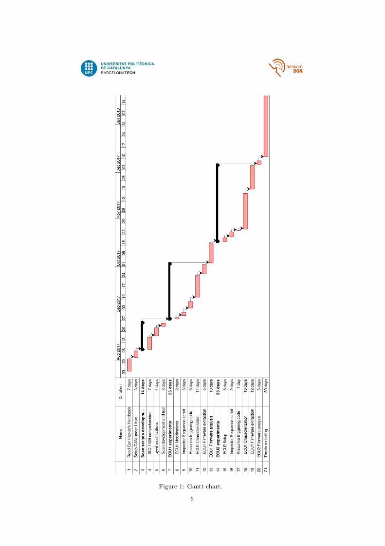
Figure 1: Gantt chart.
6

and set-top boxes deployed in the pay-TV industry. Riscure is also interna-tional market leader in providing test equipment for side channel robustnessof chip technology. Riscure laboratory equipment is used by chip manufactur-ers, government agencies and security test laboratories around the world. Inorder to achieve the main objectives, it is needed experience and backgroundin automotive embedded systems, along with deep knowledge in fault injectiontechniques and adequate equipment to perform experiments, and Riscure pro-vided the needed experience, supervision and support during the research.
7

2 State of the Art
This section will discuss the techniques known as Side Channel Attacks, usedin this work to assess the security of complex electronic automotive systems.
2.1 Side Channels
When evaluating a secure application, even when the application itself is con-sidered secure, the implementation of it is not implied to be secure. The wayan application is implemented on a device can make it vulnerable. Side channelattacks rely on physical aspects of the implementation, instead of theoreticalvulnerabilities of the implemented application itself. The name of side channelis given because of the use of unintended physical channels, intrinsic to the im-plementation, to interact with the application itself. Different ways of exploitingthe implementation aspects of a target have been proposed in [2].
In [3] there are described two common criteria to categorize these attacks.The first criterion is whether the attack is passive or active:
• Passive attacks: In this kind of attack, the device under attack runs mostlyor entirely under normal circumstances. The device is compromised byobserving physical properties of the device operation (e.g. execution time,power consumption, electromagnetic emissions).
• Active attacks: In these attacks the device, its inputs, and/or its environ-ment are manipulated in a way such the device behave abnormally. Thedevice is then compromised exploiting undefined or undesired behavior.
The second criterion for categorizing SCA is the interface used to attack thedevice. A device may have several interfaces, logical or physical. Based on theinterface used and the easiness to access it, it is possible to distinguish betweeninvasive, semi-invasive and non-invasive attacks:
• Invasive attacks: In these kind of attacks there is essentially no limit interms of interfacing and exploiting. Invasive attacks typically start withthe decapsulation of the device, and followed with high technology passiveor active techniques.Among the passive invasive attacks, microprobing is one of the most com-mon. Invasive active techniques worth mentioning are modifications usinglaser cutters or focused ion beams.The equipment needed for this attack is expensive, and they are rarelyperformed.
• Semi-Invasive attacks: In these attacks, the target device is usually alsodecapsulated, but in contrast with invasive attacks, in semi-invasive at-tacks no direct electrical contact is made.Passive semi-invasive attacks are usually related with reading memory cellswithout probing. Active semi-invasive attacks are intended to introducefaults in the device using electromagnetic fields or light.These attacks typically do not require equipment as expensive as invasiveattacks, but the effort and time needed to conduct them are relativelyhigh.
8
• Non-Invasive attacks: In these kind of attacks the device is attacked as is,without modification and exploiting only the directly accessible interfaces.Passive non-invasive attacks are usually known as side-channel analysis,and the most popular types are timing analysis attacks, power analysis at-tacks and electromagnetic (EM) analysis attacks. The idea behind thesetechniques is to compromise a device by measuring its execution time,its power consumption or its electromagnetic emissions, relating the mea-sured traces to the operation running in the target. On the other hand,active non-invasive attacks are frequently known as fault injection (FI)attacks. The main objective for FI attacks is to introduce a fault into adevice that results in unexpected or undesired behavior without the needof heavily modify the target. The most used techniques to inject faultsare clock glitching, power glitches, electromagnetic fault injection (EMFI)and Optical fault injection.Most of these attacks can be performed with inexpensive equipment incomparison with invasive attacks and even with semi-invasive attacks.Hence, non-invasive attacks are a major threat to devices security.
2.2 Fault Injection Techniques
As discussed, FI attacks are active side channel attacks. The main idea of faultinjection attacks is to deliberately put the device under stress by perturbing itsworking conditions through different methods [4].
2.2.1 Clock Glitching
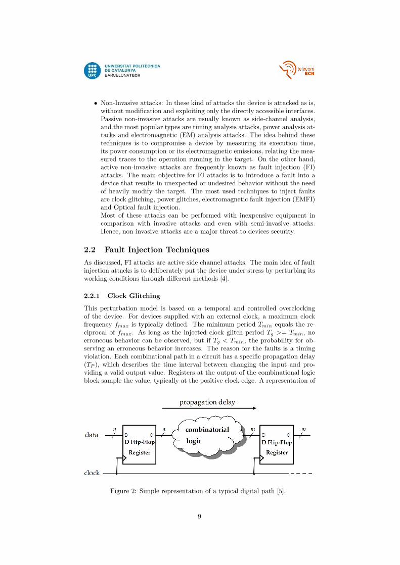
This perturbation model is based on a temporal and controlled overclockingof the device. For devices supplied with an external clock, a maximum clockfrequency fmax is typically defined. The minimum period Tmin equals the re-ciprocal of fmax. As long as the injected clock glitch period Tg >= Tmin, noerroneous behavior can be observed, but if Tg < Tmin, the probability for ob-serving an erroneous behavior increases. The reason for the faults is a timingviolation. Each combinational path in a circuit has a specific propagation delay(TP ), which describes the time interval between changing the input and pro-viding a valid output value. Registers at the output of the combinational logicblock sample the value, typically at the positive clock edge. A representation of
Figure 2: Simple representation of a typical digital path [5].
9

Figure 3: Clock glitch example.
this is provided in Figure 2. If the positive clock edge arrives before the outputof the combinational logic has settled to a stable value due to a timing violationenforced by a clock glitch (Tg < TP ), the registers store erroneous values leadingto faulty computations as a consequence [6].
For achieving this, a clock period such as Tg << Tmin < Tn is inserted,with the intention that it causes a transient malfunction of the target as theresult of a critical path timing violation. The clock signal is usually generatedas described in Figure 3. Notice that after injecting a glitch, the following clockperiod is reduced from Tn to Tn − Tg. However, given that Tg << Tn, thispost-glitch period does not affect the normal behavior of the target [7].Obviously, these kind of attacks require access to the target device clock signal,and modern microcontrollers usually synthesize different internal clock signalsfor several domains from an external reference clock, so clock glitching is notpossible, at least in a non-invasive attack.
2.2.2 Voltage Glitching
This perturbation model is based on a temporal and controlled underpoweringof the device. Underpowering means to reduce the value of the supply voltageof the attacked device below the minimum value the device is specified for.
Consider a simple CMOS inverter gate as shown in Figure 4. According to[8], it is possible to recall the propagation delay tpLH (Equation 1) as a functionof the power supply by means of a first order analysis of the inverter dynamics:
tpLH =CL[
2|Vth,p|VDD−|Vth,p| + ln(3− 4
|Vth,p|VDD
)]
µpCoxWp
Lp(VDD − |Vth,p|)
(1)
where VDD is the power supply voltage, CL the load capacitance, Vth,p thePMOS threshold voltage, µp the holes mobility, Cox the gate oxyde capacitanceand (Wp/Lp) the aspect ratio of the PMOS. A similar equation for tpHL may bederived from Equation 1 by substituting the parameters related to the inverterNMOS transistor for those related to the PMOS. Note that tpHL and tpLH mayhave different values. Hence, the data propagation time through the inverter(and through any logic block) depends on the handled data: the propagation
10

Figure 4: Inverter: architecture and waveforms.
time is data-dependent.
As stated by Equation 1 any decrease of VDD will induce an increase ofthe propagation delay of the inverter. By extension, the data propagation timethrough any logic block is increased as long as the IC is underpowered. Hence,underpowering is a valid technique to achieve fault injection by violation of thetiming constraints [9]. Due to this fact, similar effects can be achieved whenglitching the clock signal and the supply voltage [6].
Voltage glitching attacks usually need minor modifications on the targetdevice [10], such as:
• Power cut: the target IC needs to be disconnected from the on-boardpower supply, and then obtain control over the target voltage supply.
• Capacitance: the target capacitance impacts the effectiveness of the in-jected glitch. Therefore, the capacitance is reduced to a minimum byremoving as many bypass capacitors as possible from the PCB.
Nevertheless, there are other characteristics present in modern devices thatprevent voltage glitching attacks, such as on-die voltage regulators, multiplepower domains and active countermeasures such as voltage sensors. The pres-ence of regulators in the IC makes the attack drastically more difficult, as theinjected glitch becomes compensated by those regulators.
2.2.3 Electromagnetic Fault Injection
This perturbation model is based on a temporal and controlled electromagneticpulse over the device. By means of electromagnetic induction, the pulse inducesa current in the target. This current momentarily changes the voltages and logicvalues of the internal gates, and this may lead to a computational fault in thetarget [11].
Electromagnetic induction is caused by the interaction between electric fieldsand magnetic fields, according to Ampere’s circuital law and the Maxwell-Faraday equations. Alternating the polarity of a magnetic field in time causesan electric field to be generated. The consequence of this is, if a varying mag-netic field flux passes through a closed circuit, then a current is generated in
11

Figure 5: Schematic view of a loop of electrical wire with a current I in clockwisedirection The current generates a magnetic field B and B′.
that circuit. Figure 5 shows a schematic view of the effect of a magnetic fieldon a ring-shaped conductor. If the strength of the flux (i.e. number of B linescrossing the loop area) is changed, then the current I in the ring will changeas well. If the polarity of the flux is changed then the direction of the currentis switched as well. Similarly, a varying magnetic field can be generated byvarying the current in a ring-shaped conductor [12].
The intensity of the magnetic field B generated at the center of a ring-shapedconductor with radius R and constant current I can be calculated using Equation2:
B =µoµrI
4πR2
∮dL =
µoµrI
4πR22πR =
µoµrI
2R(2)
where µo is the magnetic permeability of vacuum and µr is the relative per-meability of the material the loop is filled with. Homogeneously, the currentinduced in a loop by a magnetic field B can be calculated using Maxwell-FaradayEquation, described in Equation 3:
∮δΣ
E dl = −∫
Σ
∂B
∂tdS (3)
where Σ is the surface bounded by the loop, with contour δΣ and E is theelectrical field. If we assume that the surface does not change (i.e. the conductorloop geometry remains constant in time) we can rewrite Equation 3:∮
δΣ
E dl = − ∂
∂t
∫Σ
B dS = − ∂
∂tΦB (4)
where ΦB is the value for the magnetic flux through Σ.
Equation 4 implies that an electric field can be injected in a closed circuitby varying over time the magnetic flux traversing the surface identified by thecircuit itself, hence the time partial derivative term on the right side of theEquation 4. The electric field generates a difference of potentials across differ-ent parts of the circuit, which induces currents as the free charges move to follow
12
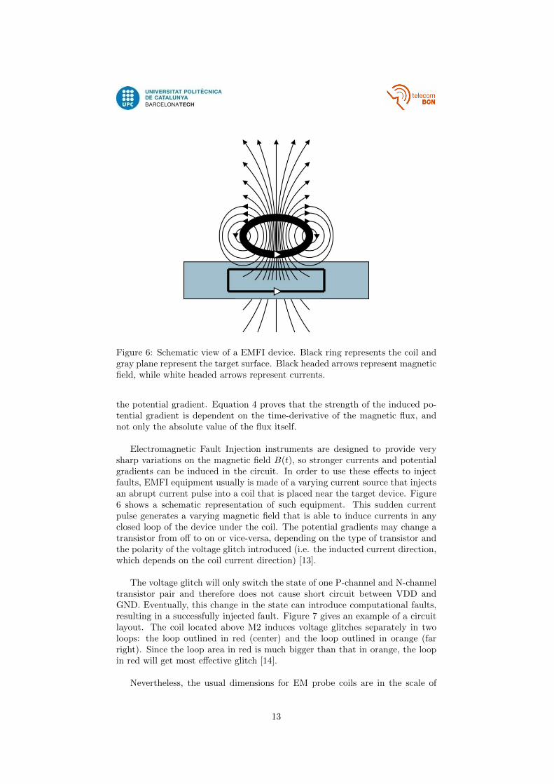
Figure 6: Schematic view of a EMFI device. Black ring represents the coil andgray plane represent the target surface. Black headed arrows represent magneticfield, while white headed arrows represent currents.
the potential gradient. Equation 4 proves that the strength of the induced po-tential gradient is dependent on the time-derivative of the magnetic flux, andnot only the absolute value of the flux itself.
Electromagnetic Fault Injection instruments are designed to provide verysharp variations on the magnetic field B(t), so stronger currents and potentialgradients can be induced in the circuit. In order to use these effects to injectfaults, EMFI equipment usually is made of a varying current source that injectsan abrupt current pulse into a coil that is placed near the target device. Figure6 shows a schematic representation of such equipment. This sudden currentpulse generates a varying magnetic field that is able to induce currents in anyclosed loop of the device under the coil. The potential gradients may change atransistor from off to on or vice-versa, depending on the type of transistor andthe polarity of the voltage glitch introduced (i.e. the inducted current direction,which depends on the coil current direction) [13].
The voltage glitch will only switch the state of one P-channel and N-channeltransistor pair and therefore does not cause short circuit between VDD andGND. Eventually, this change in the state can introduce computational faults,resulting in a successfully injected fault. Figure 7 gives an example of a circuitlayout. The coil located above M2 induces voltage glitches separately in twoloops: the loop outlined in red (center) and the loop outlined in orange (farright). Since the loop area in red is much bigger than that in orange, the loopin red will get most effective glitch [14].
Nevertheless, the usual dimensions for EM probe coils are in the scale of
13
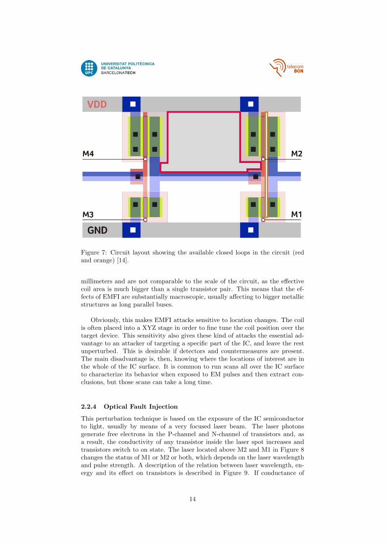
Figure 7: Circuit layout showing the available closed loops in the circuit (redand orange) [14].
millimeters and are not comparable to the scale of the circuit, as the effectivecoil area is much bigger than a single transistor pair. This means that the ef-fects of EMFI are substantially macroscopic, usually affecting to bigger metallicstructures as long parallel buses.
Obviously, this makes EMFI attacks sensitive to location changes. The coilis often placed into a XYZ stage in order to fine tune the coil position over thetarget device. This sensitivity also gives these kind of attacks the essential ad-vantage to an attacker of targeting a specific part of the IC, and leave the restunperturbed. This is desirable if detectors and countermeasures are present.The main disadvantage is, then, knowing where the locations of interest are inthe whole of the IC surface. It is common to run scans all over the IC surfaceto characterize its behavior when exposed to EM pulses and then extract con-clusions, but those scans can take a long time.
2.2.4 Optical Fault Injection
This perturbation technique is based on the exposure of the IC semiconductorto light, usually by means of a very focused laser beam. The laser photonsgenerate free electrons in the P-channel and N-channel of transistors and, asa result, the conductivity of any transistor inside the laser spot increases andtransistors switch to on state. The laser located above M2 and M1 in Figure 8changes the status of M1 or M2 or both, which depends on the laser wavelengthand pulse strength. A description of the relation between laser wavelength, en-ergy and its effect on transistors is described in Figure 9. If conductance of
14
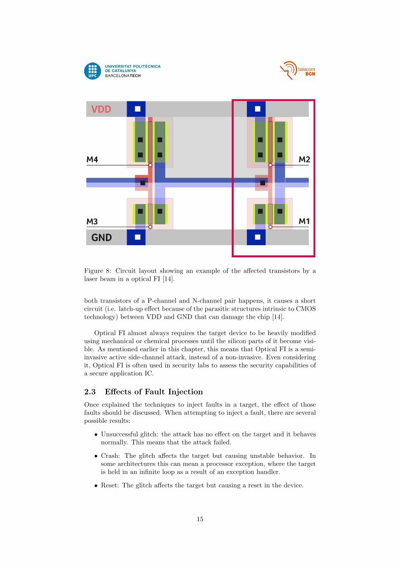
Figure 8: Circuit layout showing an example of the affected transistors by alaser beam in a optical FI [14].
both transistors of a P-channel and N-channel pair happens, it causes a shortcircuit (i.e. latch-up effect because of the parasitic structures intrinsic to CMOStechnology) between VDD and GND that can damage the chip [14].
Optical FI almost always requires the target device to be heavily modifiedusing mechanical or chemical processes until the silicon parts of it become visi-ble. As mentioned earlier in this chapter, this means that Optical FI is a semi-invasive active side-channel attack, instead of a non-invasive. Even consideringit, Optical FI is often used in security labs to assess the security capabilities ofa secure application IC.
2.3 Effects of Fault Injection
Once explained the techniques to inject faults in a target, the effect of thosefaults should be discussed. When attempting to inject a fault, there are severalpossible results:
• Unsuccessful glitch: the attack has no effect on the target and it behavesnormally. This means that the attack failed.
• Crash: The glitch affects the target but causing unstable behavior. Insome architectures this can mean a processor exception, where the targetis held in an infinite loop as a result of an exception handler.
• Reset: The glitch affects the target but causing a reset in the device.
15
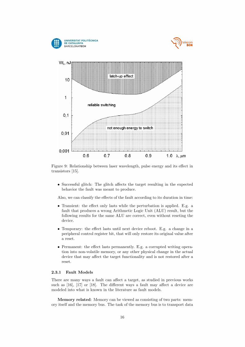
Figure 9: Relationship between laser wavelength, pulse energy and its effect intransistors [15].
• Successful glitch: The glitch affects the target resulting in the expectedbehavior the fault was meant to produce.
Also, we can classify the effects of the fault according to its duration in time:
• Transient: the effect only lasts while the perturbation is applied. E.g. afault that produces a wrong Arithmetic Logic Unit (ALU) result, but thefollowing results for the same ALU are correct, even without reseting thedevice.
• Temporary: the effect lasts until next device reboot. E.g. a change in aperipheral control register bit, that will only restore its original value aftera reset.
• Permanent: the effect lasts permanently. E.g. a corrupted writing opera-tion into non-volatile memory, or any other physical change in the actualdevice that may affect the target functionality and is not restored after areset.
2.3.1 Fault Models
There are many ways a fault can affect a target, as studied in previous workssuch as [16], [17] or [18]. The different ways a fault may affect a device aremodeled into what is known in the literature as fault models.
Memory related: Memory can be viewed as consisting of two parts: mem-ory itself and the memory bus. The task of the memory bus is to transport data
16
and instructions to and from memory. The bus is usually composed of the dataand the address bus:
• Address bus: selects the memory location to read from or the memorylocation to store to.
• Memory data bus: transports the data stored at these locations.
Both can fail independently of each other. If there is a fault on the databus, incorrect data are presented. If the address bus is glitched, the data pre-sented will be correct but from/to the wrong location. Identifying which faultsoccurred will be hard, especially if both occur at the same time.
Registers related: Registers are an important part of the execution. Tar-get devices usually contain both special use registers and general purpose regis-ters. They can be glitched mainly causing a static corruption on the contents.Then, depending on the affected register it may lead to wrong results (e.g. ageneral purpose register was corrupted and then used in an ALU instruction) orto more sophisticated faults (e.g. corrupting the program counter register leadsto a corrupted jump, corrupting the stack pointer register leads to incorrectdata retrieving from the stack).
Instructions related: Instructions are commonly categorized into threegroups: flow control, memory operations and ALU operations. Flow controloperations include instructions like branch and jump. Memory operations ei-ther store or load data from memory. Last, ALU operations are computationaloperations. Instructions and the way they are executed are highly architecturedependent. For example, in a Von Neumann architecture, instructions have afour phases cycle for execution:
1. Fetch phase: in this phase the instruction is retrieved from memory. Herememory related faults apply, as discussed in 2.3.1, so corrupted instruc-tions can be fetched, leading to different instructions or even illegal in-structions being fetched.
2. Decode phase: in this phase the fetched instruction gets decoded, assigningmeaning to the data retrieved. A fault in this phase changes the waythe instruction is decoded, leading to different instructions or even illegalinstructions being executed. Thus, it is very hard to distinguish this faultsfrom the fetch phase faults.
3. Execution phase: Once decoded, the instruction gets executed. Faults in-troduced during the execution phase would manifest themselves by com-puting an incorrect result.
4. Store phase: The store result phase of the instruction execution cyclestores the result from the executed instruction in a register or memory. Afault during this phase would manifest itself as a corrupted or un-updatedvalue being stored.
Corrupted instructions may transform themselves into illegal instructions,causing a crash or reset; or may transform into legal (but different) instructions.
17
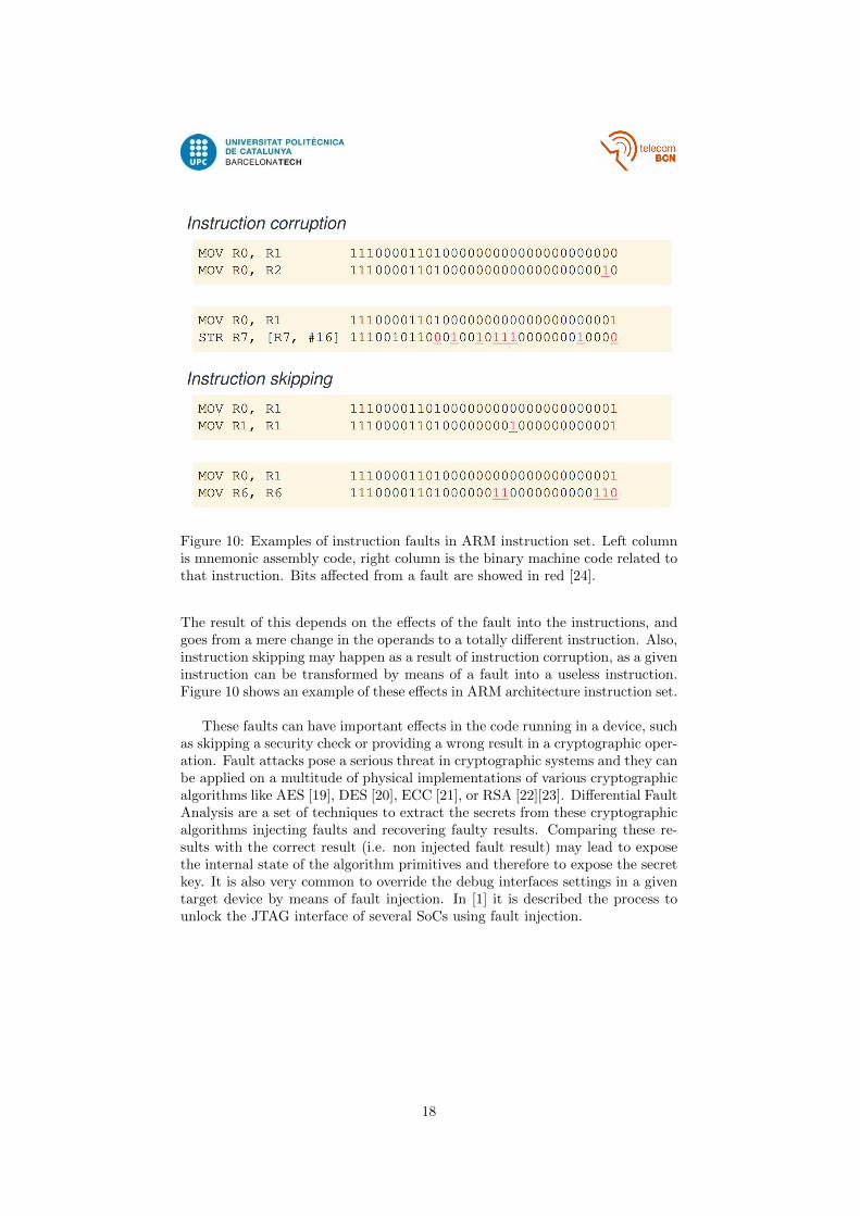
Figure 10: Examples of instruction faults in ARM instruction set. Left columnis mnemonic assembly code, right column is the binary machine code related tothat instruction. Bits affected from a fault are showed in red [24].
The result of this depends on the effects of the fault into the instructions, andgoes from a mere change in the operands to a totally different instruction. Also,instruction skipping may happen as a result of instruction corruption, as a giveninstruction can be transformed by means of a fault into a useless instruction.Figure 10 shows an example of these effects in ARM architecture instruction set.
These faults can have important effects in the code running in a device, suchas skipping a security check or providing a wrong result in a cryptographic oper-ation. Fault attacks pose a serious threat in cryptographic systems and they canbe applied on a multitude of physical implementations of various cryptographicalgorithms like AES [19], DES [20], ECC [21], or RSA [22][23]. Differential FaultAnalysis are a set of techniques to extract the secrets from these cryptographicalgorithms injecting faults and recovering faulty results. Comparing these re-sults with the correct result (i.e. non injected fault result) may lead to exposethe internal state of the algorithm primitives and therefore to expose the secretkey. It is also very common to override the debug interfaces settings in a giventarget device by means of fault injection. In [1] it is described the process tounlock the JTAG interface of several SoCs using fault injection.
18
3 Methodology
In this section it will be described the experiments performed during the researchof this work.
3.1 Objectives
As introduced in Chapter 1, the objective of the experiments is to assess thesecurity of automotive systems using fault injection techniques. Previous worksregarding security in automotive hardware make use of FI to unlock access todebug interfaces and then compromise the system [1]. The present work takesa different approach: using the automotive diagnostic services built in modernElectronic Controller Units (ECUs) as a attack vector instead. Furthermore,previous works experiments are performed under laboratory conditions, com-monly using a development board as targets, whereas the present work usescommercially available ECUs as targets.
3.2 Targets
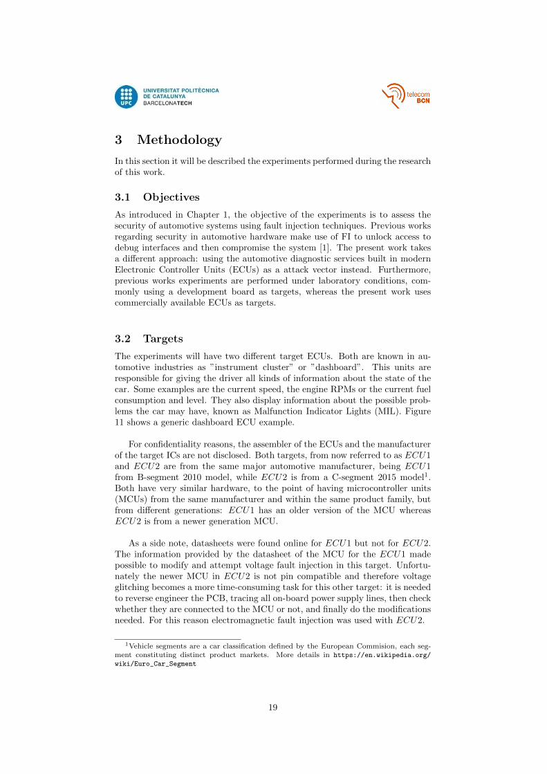
The experiments will have two different target ECUs. Both are known in au-tomotive industries as ”instrument cluster” or ”dashboard”. This units areresponsible for giving the driver all kinds of information about the state of thecar. Some examples are the current speed, the engine RPMs or the current fuelconsumption and level. They also display information about the possible prob-lems the car may have, known as Malfunction Indicator Lights (MIL). Figure11 shows a generic dashboard ECU example.
For confidentiality reasons, the assembler of the ECUs and the manufacturerof the target ICs are not disclosed. Both targets, from now referred to as ECU1and ECU2 are from the same major automotive manufacturer, being ECU1from B-segment 2010 model, while ECU2 is from a C-segment 2015 model1.Both have very similar hardware, to the point of having microcontroller units(MCUs) from the same manufacturer and within the same product family, butfrom different generations: ECU1 has an older version of the MCU whereasECU2 is from a newer generation MCU.
As a side note, datasheets were found online for ECU1 but not for ECU2.The information provided by the datasheet of the MCU for the ECU1 madepossible to modify and attempt voltage fault injection in this target. Unfortu-nately the newer MCU in ECU2 is not pin compatible and therefore voltageglitching becomes a more time-consuming task for this other target: it is neededto reverse engineer the PCB, tracing all on-board power supply lines, then checkwhether they are connected to the MCU or not, and finally do the modificationsneeded. For this reason electromagnetic fault injection was used with ECU2.
1Vehicle segments are a car classification defined by the European Commision, each seg-ment constituting distinct product markets. More details in https://en.wikipedia.org/
wiki/Euro_Car_Segment
19
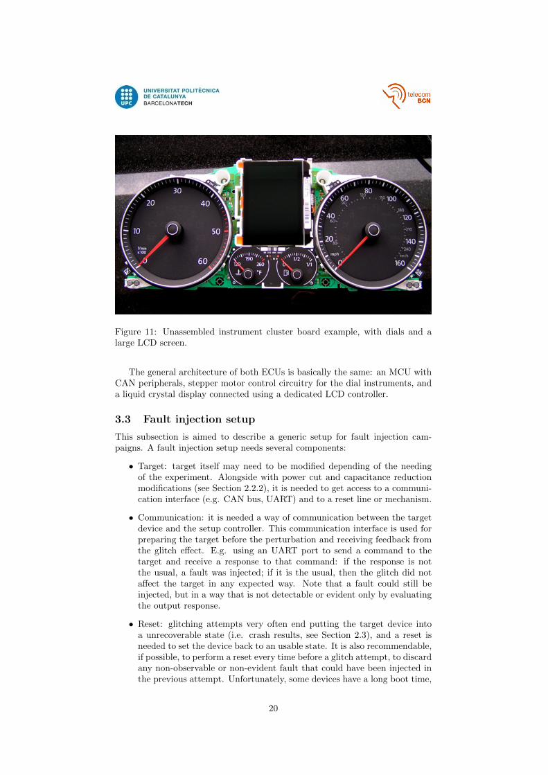
Figure 11: Unassembled instrument cluster board example, with dials and alarge LCD screen.
The general architecture of both ECUs is basically the same: an MCU withCAN peripherals, stepper motor control circuitry for the dial instruments, anda liquid crystal display connected using a dedicated LCD controller.
3.3 Fault injection setup
This subsection is aimed to describe a generic setup for fault injection cam-paigns. A fault injection setup needs several components:
• Target: target itself may need to be modified depending of the needingof the experiment. Alongside with power cut and capacitance reductionmodifications (see Section 2.2.2), it is needed to get access to a communi-cation interface (e.g. CAN bus, UART) and to a reset line or mechanism.
• Communication: it is needed a way of communication between the targetdevice and the setup controller. This communication interface is used forpreparing the target before the perturbation and receiving feedback fromthe glitch effect. E.g. using an UART port to send a command to thetarget and receive a response to that command: if the response is notthe usual, a fault was injected; if it is the usual, then the glitch did notaffect the target in any expected way. Note that a fault could still beinjected, but in a way that is not detectable or evident only by evaluatingthe output response.
• Reset: glitching attempts very often end putting the target device intoa unrecoverable state (i.e. crash results, see Section 2.3), and a reset isneeded to set the device back to an usable state. It is also recommendable,if possible, to perform a reset every time before a glitch attempt, to discardany non-observable or non-evident fault that could have been injected inthe previous attempt. Unfortunately, some devices have a long boot time,
20
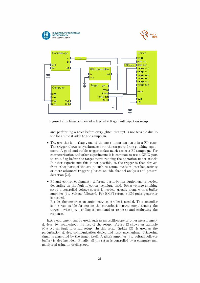
Figure 12: Schematic view of a typical voltage fault injection setup.
and performing a reset before every glitch attempt is not feasible due tothe long time it adds to the campaign.
• Trigger: this is, perhaps, one of the most important parts in a FI setup.The trigger allows to synchronize both the target and the glitching equip-ment. A good and stable trigger makes much easier a FI campaign. Forcharacterization and other experiments it is common to use a GPIO portto set a flag before the target starts running the operation under attack.In other experiments this is not possible, so the trigger is then derivedfrom other parts of the setup, such as communication interface activityor more advanced triggering based on side channel analysis and patterndetection [25].
• FI and control equipment: different perturbation equipment is neededdepending on the fault injection technique used. For a voltage glitchingsetup a controlled voltage source is needed, usually along with a bufferamplifier (i.e. voltage follower). For EMFI setups a EM pulse generatoris needed.Besides the perturbation equipment, a controller is needed. This controlleris the responsible for setting the perturbation parameters, arming thetarget device (i.e. sending a command or request) and evaluating theresponse.
Extra equipment can be used, such as an oscilloscope or other measurementdevices, to troubleshoot the rest of the setup. Figure 12 shows an exampleof a typical fault injection setup. In this setup, Spider [26] is used as theperturbation device, communication device and reset mechanism. Triggeringsignal is generated by the target itself. A glitch amplifier (i.e. voltage followerbuffer) is also included. Finally, all the setup is controlled by a computer andmonitored using an oscilloscope.
21
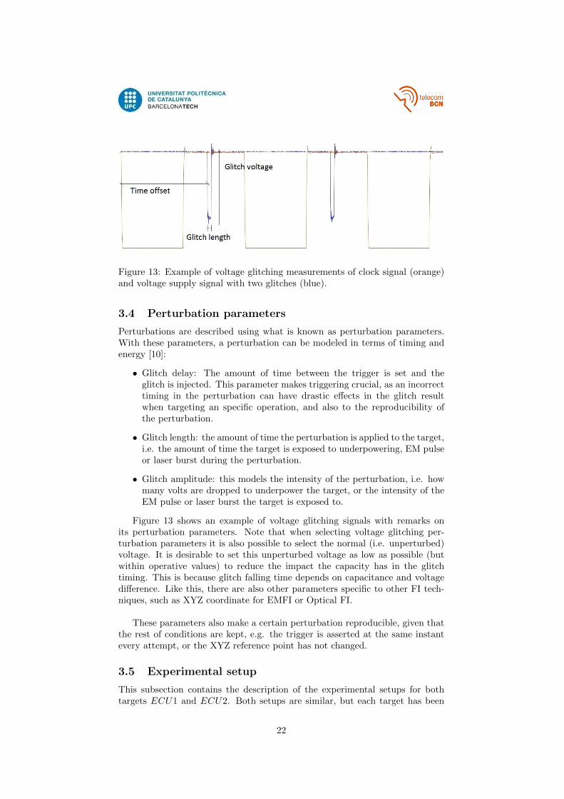
Figure 13: Example of voltage glitching measurements of clock signal (orange)and voltage supply signal with two glitches (blue).
3.4 Perturbation parameters
Perturbations are described using what is known as perturbation parameters.With these parameters, a perturbation can be modeled in terms of timing andenergy [10]:
• Glitch delay: The amount of time between the trigger is set and theglitch is injected. This parameter makes triggering crucial, as an incorrecttiming in the perturbation can have drastic effects in the glitch resultwhen targeting an specific operation, and also to the reproducibility ofthe perturbation.
• Glitch length: the amount of time the perturbation is applied to the target,i.e. the amount of time the target is exposed to underpowering, EM pulseor laser burst during the perturbation.
• Glitch amplitude: this models the intensity of the perturbation, i.e. howmany volts are dropped to underpower the target, or the intensity of theEM pulse or laser burst the target is exposed to.
Figure 13 shows an example of voltage glitching signals with remarks onits perturbation parameters. Note that when selecting voltage glitching per-turbation parameters it is also possible to select the normal (i.e. unperturbed)voltage. It is desirable to set this unperturbed voltage as low as possible (butwithin operative values) to reduce the impact the capacity has in the glitchtiming. This is because glitch falling time depends on capacitance and voltagedifference. Like this, there are also other parameters specific to other FI tech-niques, such as XYZ coordinate for EMFI or Optical FI.
These parameters also make a certain perturbation reproducible, given thatthe rest of conditions are kept, e.g. the trigger is asserted at the same instantevery attempt, or the XYZ reference point has not changed.
3.5 Experimental setup
This subsection contains the description of the experimental setups for bothtargets ECU1 and ECU2. Both setups are similar, but each target has been
22
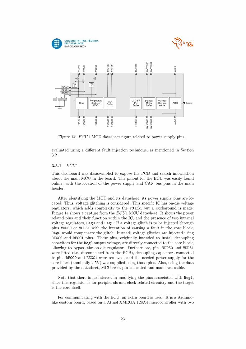
Figure 14: ECU1 MCU datasheet figure related to power supply pins.
evaluated using a different fault injection technique, as mentioned in Section3.2.
3.5.1 ECU1
This dashboard was disassembled to expose the PCB and search informationabout the main MCU in the board. The pinout for the ECU was easily foundonline, with the location of the power supply and CAN bus pins in the mainheader.
After identifying the MCU and its datasheet, its power supply pins are lo-cated. Thus, voltage glitching is considered. This specific IC has on-die voltageregulators, which adds complexity to the attack, but a workaround is made.Figure 14 shows a capture from the ECU1 MCU datasheet. It shows the powerrelated pins and their function within the IC, and the presence of two internalvoltage regulators, Reg0 and Reg1. If a voltage glitch is to be injected throughpins VDD50 or VDD51 with the intention of causing a fault in the core block,Reg0 would compensate the glitch. Instead, voltage glitches are injected usingREGC0 and REGC1 pins. These pins, originally intended to install decouplingcapacitors for the Reg0 output voltage, are directly connected to the core block,allowing to bypass the on-die regulator. Furthermore, pins VDD50 and VDD51
were lifted (i.e. disconnected from the PCB), decoupling capacitors connectedto pins REGC0 and REGC1 were removed, and the needed power supply for thecore block (nominally 2.5V) was supplied using those pins. Also, using the dataprovided by the datasheet, MCU reset pin is located and made accessible.
Note that there is no interest in modifying the pins associated with Reg1,since this regulator is for peripherals and clock related circuitry and the targetis the core itself.
For communicating with the ECU, an extra board is used. It is a Arduino-like custom board, based on a Atmel XMEGA 128A4 microcontroller with two
23
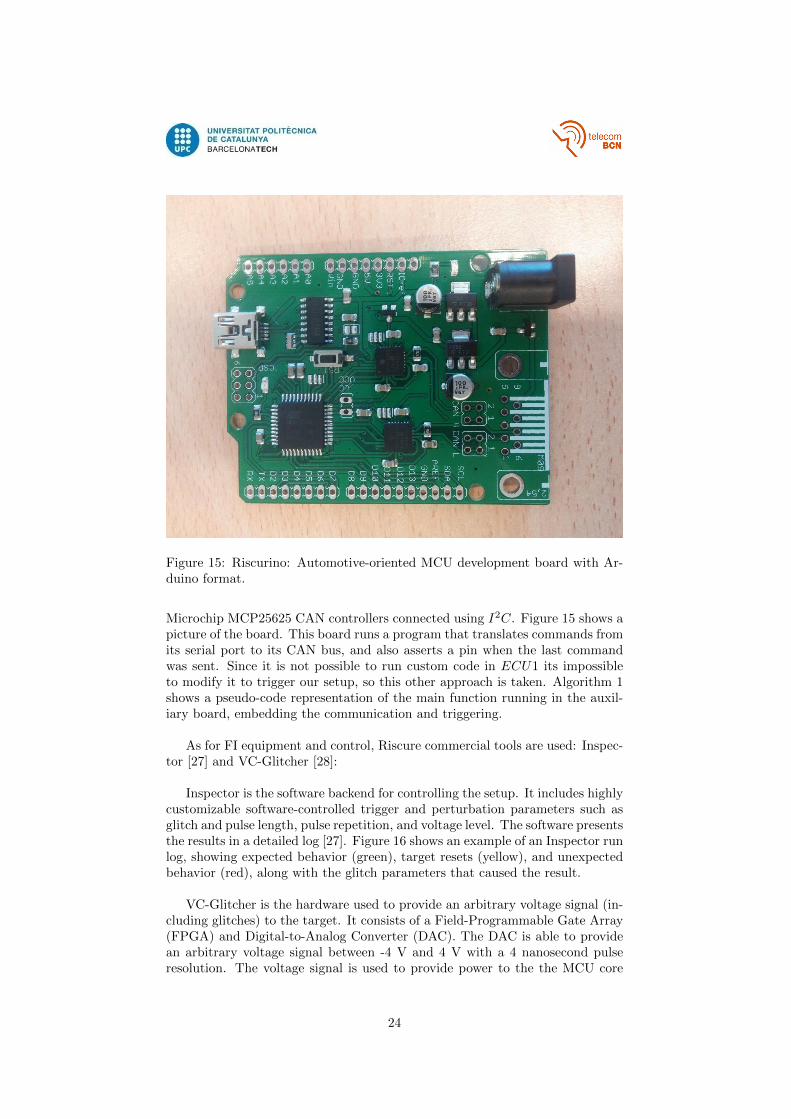
Figure 15: Riscurino: Automotive-oriented MCU development board with Ar-duino format.
Microchip MCP25625 CAN controllers connected using I2C. Figure 15 shows apicture of the board. This board runs a program that translates commands fromits serial port to its CAN bus, and also asserts a pin when the last commandwas sent. Since it is not possible to run custom code in ECU1 its impossibleto modify it to trigger our setup, so this other approach is taken. Algorithm 1shows a pseudo-code representation of the main function running in the auxil-iary board, embedding the communication and triggering.
As for FI equipment and control, Riscure commercial tools are used: Inspec-tor [27] and VC-Glitcher [28]:
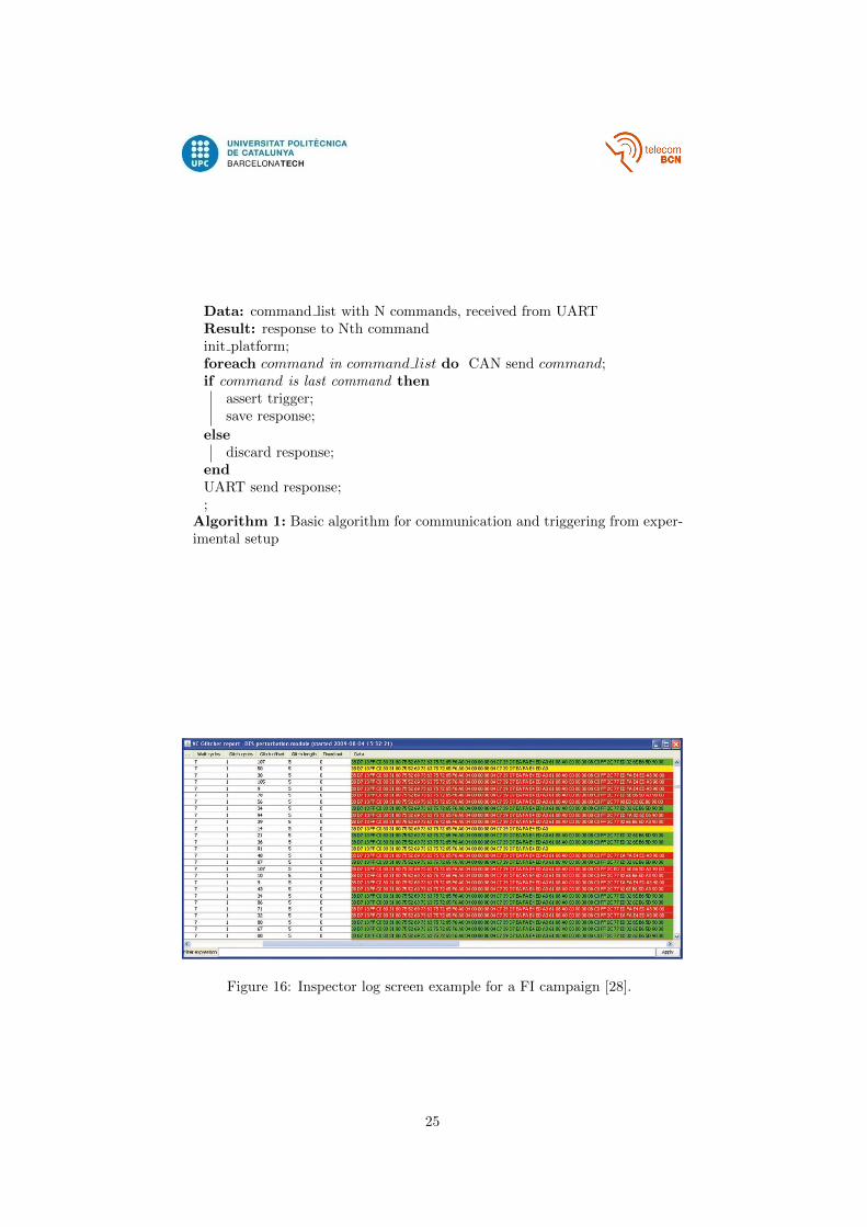
Inspector is the software backend for controlling the setup. It includes highlycustomizable software-controlled trigger and perturbation parameters such asglitch and pulse length, pulse repetition, and voltage level. The software presentsthe results in a detailed log [27]. Figure 16 shows an example of an Inspector runlog, showing expected behavior (green), target resets (yellow), and unexpectedbehavior (red), along with the glitch parameters that caused the result.
VC-Glitcher is the hardware used to provide an arbitrary voltage signal (in-cluding glitches) to the target. It consists of a Field-Programmable Gate Array(FPGA) and Digital-to-Analog Converter (DAC). The DAC is able to providean arbitrary voltage signal between -4 V and 4 V with a 4 nanosecond pulseresolution. The voltage signal is used to provide power to the the MCU core
24
Data: command list with N commands, received from UARTResult: response to Nth commandinit platform;foreach command in command list do CAN send command;if command is last command then
assert trigger;save response;
elsediscard response;
endUART send response;;
Algorithm 1: Basic algorithm for communication and triggering from exper-imental setup
Figure 16: Inspector log screen example for a FI campaign [28].
25
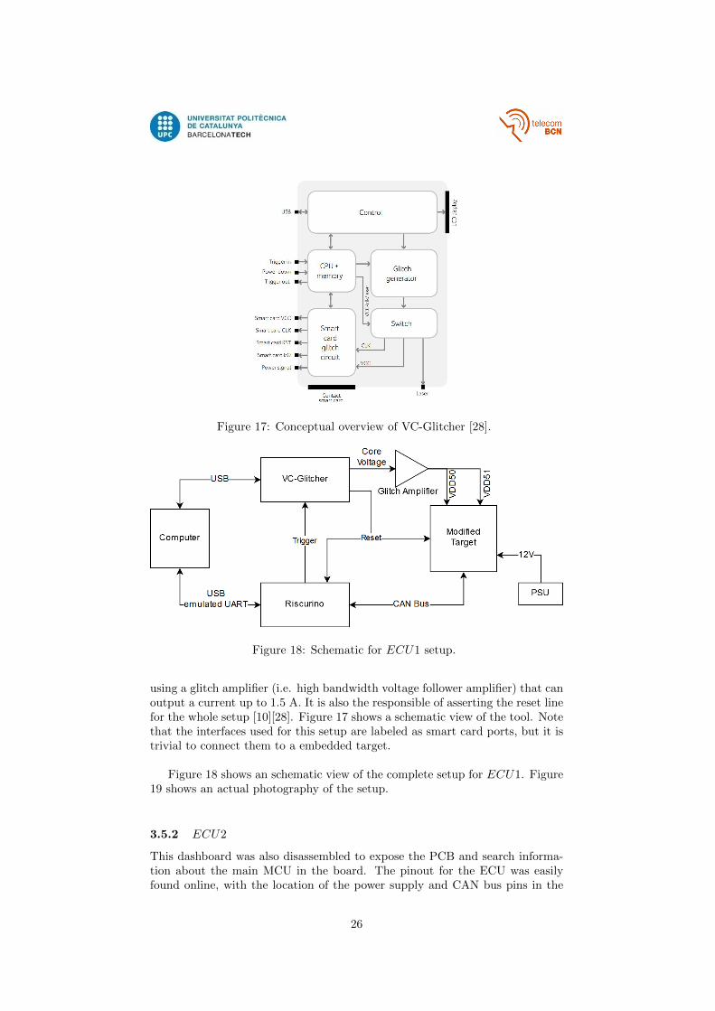
Figure 17: Conceptual overview of VC-Glitcher [28].
Figure 18: Schematic for ECU1 setup.
using a glitch amplifier (i.e. high bandwidth voltage follower amplifier) that canoutput a current up to 1.5 A. It is also the responsible of asserting the reset linefor the whole setup [10][28]. Figure 17 shows a schematic view of the tool. Notethat the interfaces used for this setup are labeled as smart card ports, but it istrivial to connect them to a embedded target.
Figure 18 shows an schematic view of the complete setup for ECU1. Figure19 shows an actual photography of the setup.
3.5.2 ECU2
This dashboard was also disassembled to expose the PCB and search informa-tion about the main MCU in the board. The pinout for the ECU was easilyfound online, with the location of the power supply and CAN bus pins in the
26
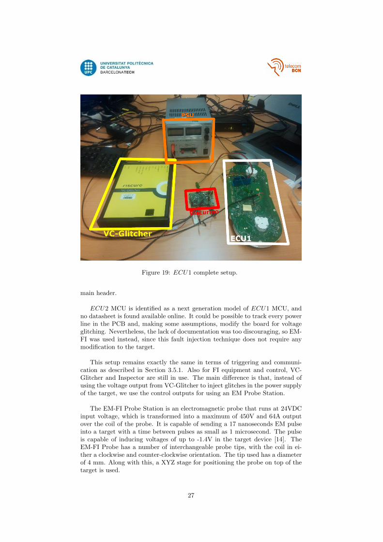
Figure 19: ECU1 complete setup.
main header.
ECU2 MCU is identified as a next generation model of ECU1 MCU, andno datasheet is found available online. It could be possible to track every powerline in the PCB and, making some assumptions, modify the board for voltageglitching. Nevertheless, the lack of documentation was too discouraging, so EM-FI was used instead, since this fault injection technique does not require anymodification to the target.
This setup remains exactly the same in terms of triggering and communi-cation as described in Section 3.5.1. Also for FI equipment and control, VC-Glitcher and Inspector are still in use. The main difference is that, instead ofusing the voltage output from VC-Glitcher to inject glitches in the power supplyof the target, we use the control outputs for using an EM Probe Station.
The EM-FI Probe Station is an electromagnetic probe that runs at 24VDCinput voltage, which is transformed into a maximum of 450V and 64A outputover the coil of the probe. It is capable of sending a 17 nanoseconds EM pulseinto a target with a time between pulses as small as 1 microsecond. The pulseis capable of inducing voltages of up to -1.4V in the target device [14]. TheEM-FI Probe has a number of interchangeable probe tips, with the coil in ei-ther a clockwise and counter-clockwise orientation. The tip used has a diameterof 4 mm. Along with this, a XYZ stage for positioning the probe on top of thetarget is used.
27
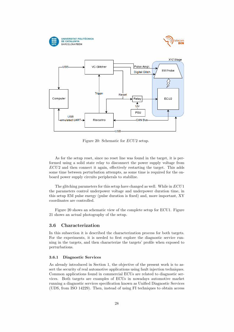
Figure 20: Schematic for ECU2 setup.
As for the setup reset, since no reset line was found in the target, it is per-formed using a solid state relay to disconnect the power supply voltage fromECU2 and then connect it again, effectively restarting the target. This addssome time between perturbation attempts, as some time is required for the on-board power supply circuits peripherals to stabilize.
The glitching parameters for this setup have changed as well. While in ECU1the parameters control underpower voltage and underpower duration time, inthis setup EM pulse energy (pulse duration is fixed) and, more important, XYcoordinates are controlled.
Figure 20 shows an schematic view of the complete setup for ECU1. Figure21 shows an actual photography of the setup.
3.6 Characterization
In this subsection it is described the characterization process for both targets.For the experiments, it is needed to first explore the diagnostic service run-ning in the targets, and then characterize the targets’ profile when exposed toperturbations.
3.6.1 Diagnostic Services
As already introduced in Section 1, the objective of the present work is to as-sert the security of real automotive applications using fault injection techniques.Common applications found in commercial ECUs are related to diagnostic ser-vices. Both targets are examples of ECUs in nowadays automotive marketrunning a diagnostic services specification known as Unified Diagnostic Services(UDS, from ISO 14229). Then, instead of using FI techniques to obtain access
28
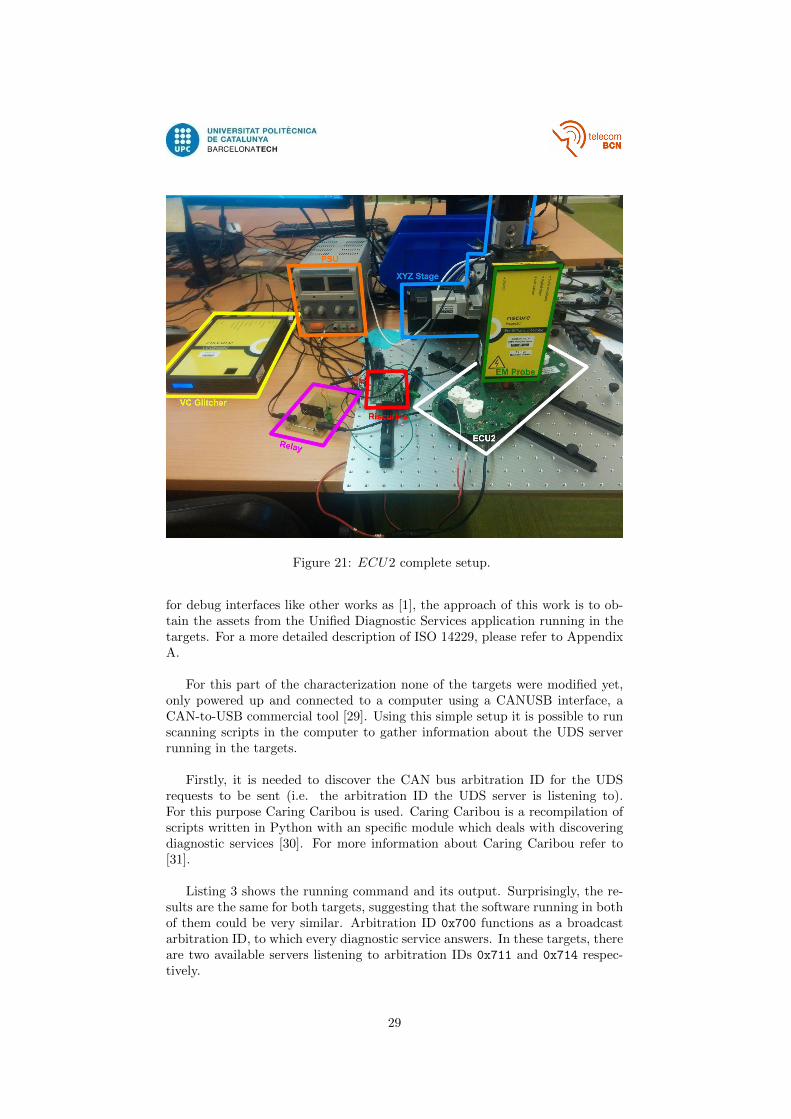
Figure 21: ECU2 complete setup.
for debug interfaces like other works as [1], the approach of this work is to ob-tain the assets from the Unified Diagnostic Services application running in thetargets. For a more detailed description of ISO 14229, please refer to AppendixA.
For this part of the characterization none of the targets were modified yet,only powered up and connected to a computer using a CANUSB interface, aCAN-to-USB commercial tool [29]. Using this simple setup it is possible to runscanning scripts in the computer to gather information about the UDS serverrunning in the targets.
Firstly, it is needed to discover the CAN bus arbitration ID for the UDSrequests to be sent (i.e. the arbitration ID the UDS server is listening to).For this purpose Caring Caribou is used. Caring Caribou is a recompilation ofscripts written in Python with an specific module which deals with discoveringdiagnostic services [30]. For more information about Caring Caribou refer to[31].
Listing 3 shows the running command and its output. Surprisingly, the re-sults are the same for both targets, suggesting that the software running in bothof them could be very similar. Arbitration ID 0x700 functions as a broadcastarbitration ID, to which every diagnostic service answers. In these targets, thereare two available servers listening to arbitration IDs 0x711 and 0x714 respec-tively.
29
Now it is desirable to have a listing of every service available in those servers.Listing 4 shows the running commands and results for discovering services avail-able in both servers. Since the server listening to 0x714 has more services avail-able, it becomes the target server for the rest of the experiments. Nevertheless,according to the ISO 14229 services are sometimes available only under certainsession. Caring Caribou lacks the functionality for scanning session codes andthe services available in each session. For this, a custom scanning script wasmade, based on pyvit [32] (formerly known as CANard [33]). pyvit is a toolkitfor interfacing with automotive hardware from Python. It aims to implementcommon hardware interfaces and protocols used in the automotive systems.
A typical UDS operation starts with a client (i.e. tester that makes use ofthe diagnostic services) sending a request to the server (i.e. part of an ECUand that provides the diagnostic services) for a certain diagnostic service, iden-tified by its service ID. The server then sends a response to the client, that canbe either positive, meaning that the requested operation was successful; or anegative response, meaning that the request could not be fulfilled. Positive re-sponses contain the result of the request, while negative responses contain a codeassociated with the circumstances for which the operation was not performed.
The strategy behind the services scanner is really simple: send requestsincreasing the service ID, with no sub-function nor parameters, and then obtainthe response. Then, depending on the negative response code it can be guessedif that service ID is supported or not:
• Not supported: The negative response will have a negative response codeof 0x11 (serviceNotSupported).
• Supported: Positive responses or negative responses with any other nega-tive response code different from 0x11.
Then, after obtaining a list of services, a list of session codes is needed.Again, the strategy is simple: send request of DiagnosticSessionControl in-creasing the sessionID parameter and evaluating the response code to guess ifthe session code is supported or not. Appendix A.1 shows a detailed descriptionof the DiagnosticSessionControl service. If the response is positive, servicesfound to be supported in the previous scan are requested again, to check whetherthey are supported or not in the current session code (i.e. negative responsecode different from 0x7F (serviceNotSupportedInActiveSession).
Listing 5 shows the result of this custom scanning script. It is worth men-tioning that the available services results match the results from Caring Caribouservices scan (i.e. Listing 4).
As introduced in Section 1, firmware extraction is a main concern in hard-ware security, as the posterior analysis of the binary can expose even more vul-nerabilities. For extracting the firmware from the targets, ReadMemoryByAddress(Service ID 0x23) is the most suitable service, since it allows to recover the con-tent of physical addresses. Appendix A.2 shows a detailed description of theReadMemoryByAddress service.
30
The first step for using this service is being in a diagnosticSession inwhich ReadMemoryByAddres is available. According to the scans performed,diagnosticSession 0x4F has access to this service, so a diagnosticSessionControlrequest with sessionID parameter set to 0x4F is sent, obtaining a positive re-sponse. From this session it is possible to make ReadMemoryByAddres requests.But after any read request for any portion of memory, the response is nega-tive, with a negative response code of 0x33 (i.e. SecurityAccessDenied). Thismeans that the service is protected and a successful SecurityAccess request isfirst needed to get to use ReadMemoryByAddress.
SecurityAccess service allows clients to authenticate and grants access todifferent services with protected access, such as the service ReadMemoryByAddress.This authentication is based on a challenge-response scheme. First a seed is re-quested, then an algorithm known for both client and server transforms the seed.This algorithm is not defined by the ISO 14229 standard, so manufacturers arefree to design and implement their own algorithm, which is usually confidentialand not publicly available. Last, the result from applying the challenge algo-rithm to the seed is sent back to the server as a key in a new request. At theserver, if the key matches with the expected result, security access is granted tothe client. Every time a wrong key is entered a new seed is generated to avoidbrute-force attacks. Also, a new seed is generated every time the target is re-seted. This protection mechanism are not required by the ISO 14229 standard,so they are an implementation decision from the targets manufacturer. Moredetails about SecurityAccess service can be found in Appendix A.3.
SecurityAccess itself could be a target for an attacker. A successful glitchat the right instant could bypass the key comparison instruction and grantaccess to an attacker that does not know the challenge algorithm. For thesetargets not the case: after 3 wrong keys, there is a timeout of 10 minutes untilthe next authentication attempt. Moreover, this timeout is also run after everyboot as well (i.e. no authentication requests are possible within the first 10 min-utes from power up), so the timeout cannot be avoided by resetting the target.This timeout is described in the ISO 14229 standard, but it is not mandatory.The vehicle manufacturer shall then select if the delay timer is supported or not.
Considering the options, the final approach is trying to glitch at the au-thentication checking that happens in the server after a ReadMemoryByAddress
request. Again, a successful glitch at the right instant could bypass the authen-tication status check instruction, posing as autheticated and therefore allowingthe ReadMemoryByAddress service execution. This would allow an attacker toreceive the memory content even when not authenticated.
3.6.2 FI characterization
Before attempting to glitch a target, it is customary to first obtain a set ofperturbation parameters that optimize the faults injection process. This pa-rameters are obtained in an experimental way, running an example programwith predictable timing and result. For example, in [1] the authors approachedthe FI characterization using two different experiments, both with predictable
31
result and with a stable trigger signal:
• unroll experiment: a sequence of increment instructions is performed onthe same CPU register. This should produce a predictable final value inthe counter register. The final value of the register is sent over a serialconnection at the end of the sequence. A pseudo code version of this setupis given in Listing 1. A successful glitch affects the value of the counterregister by altering the content of the register itself or by changing thecode flow and skipping one (or more) increment instruction(s).
• auth experiment: an if-statement determines the program flow, simulatinga situation where an authentication check is performed, as shown in Listing2. A successful glitch affects the if-statement so the unintended branch(i.e. send serial authenticated function call) is executed.
Listing 1: unroll scenario pseudocode [1]
trigger_up()
asm(add r1 #1)
asm(add r1 #1)
...
asm(add r1 #1)
asm(add r1 #1)
trigger_down()
send_serial(r1)
Listing 2: auth scenario pseudocode [1]
flag = 1
...
trigger_up()
if (flag == 0):
send_serial_authenticated()
else
send_serial_denied()
trigger_down()
The methodology used for finding the optimal parameters (i.e. those withthe highest success rate) involves running multiple FI campaigns. In each cam-paign, thousands of glitches are attempted while varying the parameters withina certain range. The initial FI campaign runs on very broad parameters. Theparameters of the successful glitches found are used to restrict the search rangein the next campaign and after few iterations of this process the optimal pa-rameters are found.
It is not possible to run custom code in the target devices: programmingtools and documentation are missing, and even with those, the firmware thatis to be extracted would be erased from the targets if any experiment code isflashed. Therefore, it is impossible to run experiments like unroll or auth.The main problem behind this is the impossibility to obtain a trigger signal,controlled and synchronized with the characterization experiment. In this case,
32
other triggering mechanisms are used, such as triggering based on communica-tion traffic events.
For triggering the setup the auxiliary board Riscurino is used. It sets thetrigger after sending the UDS ReadMemoryByAddress request, and clears thetrigger after receiving any response. Figure 22 shows DSO measurements over-lapped over time for both the trigger line and CAN high line for ECU1. It canbe appreciated the time between the trigger asserting and the server responsetransmission (second group of activity, near the measuring cursors). That pe-riod is the whole time window for the glitch offset parameter. Similar behaviorwas measured for ECU2 but with different timing values.
It is also worth mentioning that the persistence view of the scope shows jitterin the response timing. This jitter is shown in the Figure 22 between the timeaxis cursors, caused by variations in the timing between the trigger assertingand the response transmission. This variations can have an origin in the targetfirmware, which probably is based on a Real Time Operating System (RTOS)solution with different scheduled tasks sharing the resources of the MCU. ARTOS scheduler could explain the measured jitter. This jitter is an inconve-nience in terms of reproducibility, as the relative time between the triggeringand the computation of the response is not constant and therefore there is alimit for the glitch offset parameter narrowing.
For the rest of perturbation parameters, such as glitch voltage, glitch lengthfor ECU1 or pulse intensity for ECU2, broad but yet reasonable ranges weredefined. As for the XYZ coordinates in the case of ECU2, a squared scan areawas defined in the inner part of the package, focusing on the die location andskipping the bonding wires area.
3.6.3 ECU1
For the first voltage glitching campaign the following perturbation parametersare selected:
• Glitch Offset: Random within 783,79 µs and 1299,59 µs (515 µs wide)
• Glitch Voltage: Random within -1 V and -0.7 V (relative to VCC = 2.3V )
• Glitch Length: Random within 150 ns and 350 ns
After a small number of glitch attempts a successful glitch was injected. Fig-ure 23 shows a plot of the results. Each dot in the plots represents a FI attempt,and the color of the dot represents the result: no effect (green), restart or mute(yellow) and successful glitch (red). The three different plots show all threevariable (i.e. randomized) parameters against each other. Note that the glitchoffset time window is about 515 µs, and each glitch offset step has a resolutionof 2 ns, so there is a great amount of possible values. It is not usual to extractconclusions after such a small number of attempts, but with such a broad glitchoffset time window it is desirable to reduce it as soon as possible and not tospend more attempts in parameter values that have no desired effect on the
33
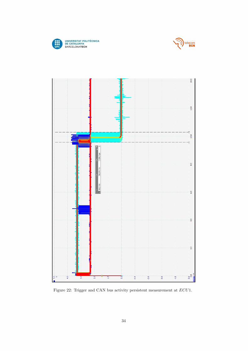
Figure 22: Trigger and CAN bus activity persistent measurement at ECU1.
34

target. Therefore, it is considered that the optimal glitch offset parameter valueis more likely to be near the value of that single successful glitch.
The next experiment keeps all the parameters equal to the previous one, butreducing the glitch offset time window to 9 µs wide and centered on the firstsuccessful glitch offset value:
• Glitch Offset: Random within 1050 µs and 1059 µs (9 µs wide)
• Glitch Voltage: Random within -1 V and -0.7 V (relative to VCC = 2.3V )
• Glitch Length: Random within 150 ns and 350 ns
The results after almost 150k glitch attempts are shown in Figure 24. Addi-tional colors such as cyan, magenta and orange shows unexpected, non-successfulresponses. The final successful glitch rate is about 0.5%.
Figure 24 shows that there is a quasi-linear relation in the glitch energy pa-rameters (i.e. glitch voltage times glitch time), and for reducing these parame-ters a smaller area is selected, keeping in mind the mentioned linear relationship.As for the glitch offset, glitches are rarely taking place past the 1055 µs value,so a new and narrower time window is defined for the next experiment:
• Glitch Offset: Random within 1052 µs and 1055 µs (3 µs wide)
• Glitch Voltage: Random within -0.85 V and -0.8 V (relative to VCC =2.3V )
• Glitch Length: Random within 250 ns and 274 ns
Figure 25 shows the results for the third and last experiment, which in lessthan 15k glitch attempts achieved a successful glitch rate of 0.88%.
Table 1 show a summary of ECU1 experiments parameters and hit rate:
3.6.4 ECU2
For the first EM-FI experiment the following perturbation parameters are se-lected:
• Glitch Offset: Random within 260 µs and 420 µs (160 µs wide)
• Glitch Power: Random within 25% and 55% of EM probe maximum power
• XY coordinates: defined a grid of 30x15 points over the inner part of theIC.
Table 1: ECU1 experiments summary# Glitch Offset Glitch Voltage Glitch Length Hit rate1 [783.79, 1299.59] us [-1, -0.7] V [150, 350] ns N/A2 [1050, 1059] us [-1, -0.7] V [150, 350] ns 0.50%3 [1052, 1055] us [-0.85, -0.8 ] V [250, 274] ns 0.88%
35
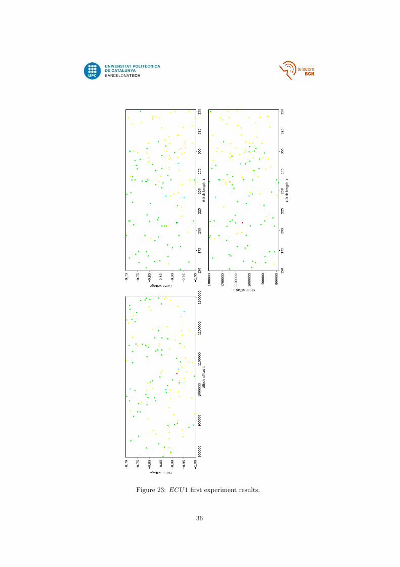
Figure 23: ECU1 first experiment results.
36
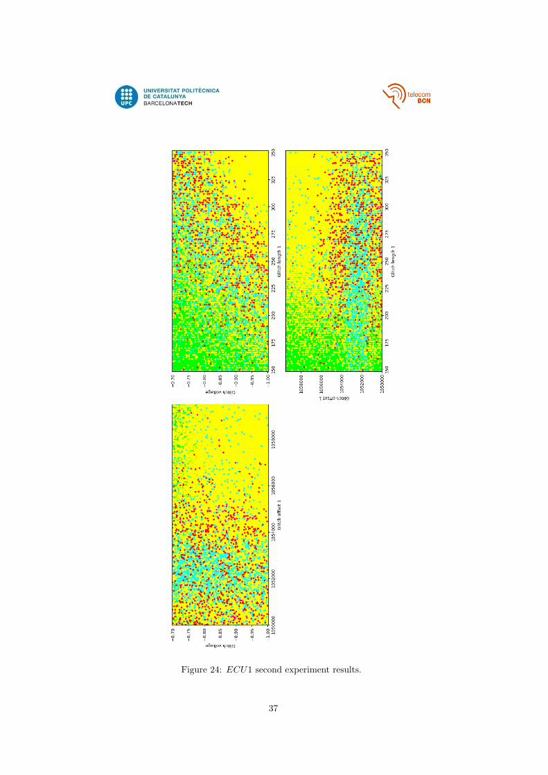
Figure 24: ECU1 second experiment results.
37
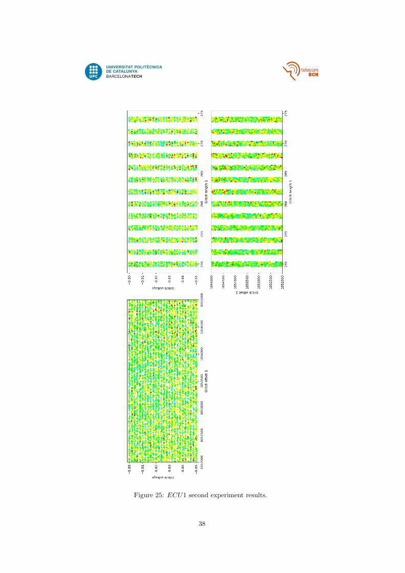
Figure 25: ECU1 second experiment results.
38
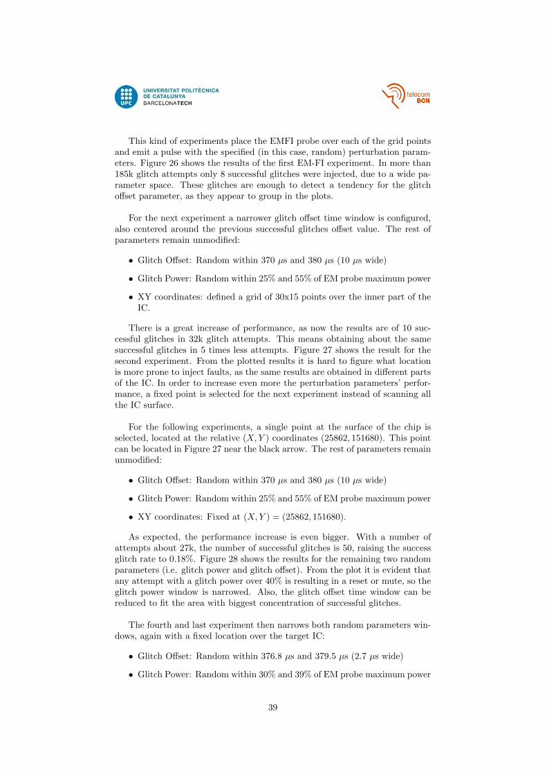
This kind of experiments place the EMFI probe over each of the grid pointsand emit a pulse with the specified (in this case, random) perturbation param-eters. Figure 26 shows the results of the first EM-FI experiment. In more than185k glitch attempts only 8 successful glitches were injected, due to a wide pa-rameter space. These glitches are enough to detect a tendency for the glitchoffset parameter, as they appear to group in the plots.
For the next experiment a narrower glitch offset time window is configured,also centered around the previous successful glitches offset value. The rest ofparameters remain unmodified:
• Glitch Offset: Random within 370 µs and 380 µs (10 µs wide)
• Glitch Power: Random within 25% and 55% of EM probe maximum power
• XY coordinates: defined a grid of 30x15 points over the inner part of theIC.
There is a great increase of performance, as now the results are of 10 suc-cessful glitches in 32k glitch attempts. This means obtaining about the samesuccessful glitches in 5 times less attempts. Figure 27 shows the result for thesecond experiment. From the plotted results it is hard to figure what locationis more prone to inject faults, as the same results are obtained in different partsof the IC. In order to increase even more the perturbation parameters’ perfor-mance, a fixed point is selected for the next experiment instead of scanning allthe IC surface.
For the following experiments, a single point at the surface of the chip isselected, located at the relative (X,Y ) coordinates (25862, 151680). This pointcan be located in Figure 27 near the black arrow. The rest of parameters remainunmodified:
• Glitch Offset: Random within 370 µs and 380 µs (10 µs wide)
• Glitch Power: Random within 25% and 55% of EM probe maximum power
• XY coordinates: Fixed at (X,Y ) = (25862, 151680).
As expected, the performance increase is even bigger. With a number ofattempts about 27k, the number of successful glitches is 50, raising the successglitch rate to 0.18%. Figure 28 shows the results for the remaining two randomparameters (i.e. glitch power and glitch offset). From the plot it is evident thatany attempt with a glitch power over 40% is resulting in a reset or mute, so theglitch power window is narrowed. Also, the glitch offset time window can bereduced to fit the area with biggest concentration of successful glitches.
The fourth and last experiment then narrows both random parameters win-dows, again with a fixed location over the target IC:
• Glitch Offset: Random within 376.8 µs and 379.5 µs (2.7 µs wide)
• Glitch Power: Random within 30% and 39% of EM probe maximum power
39
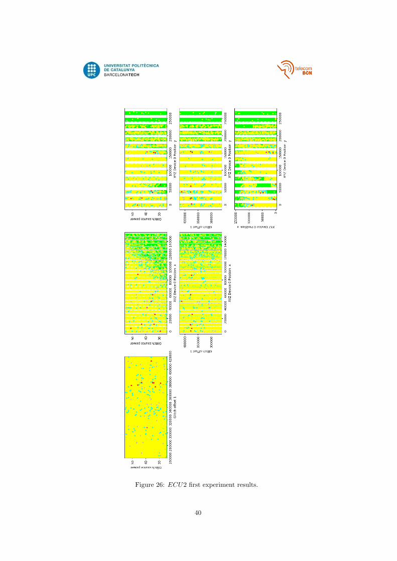
Figure 26: ECU2 first experiment results.
40
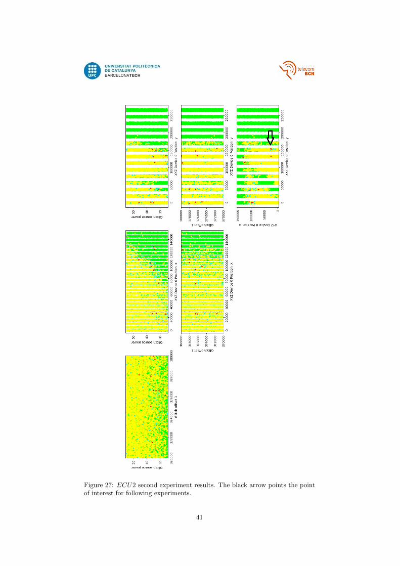
Figure 27: ECU2 second experiment results. The black arrow points the pointof interest for following experiments.
41
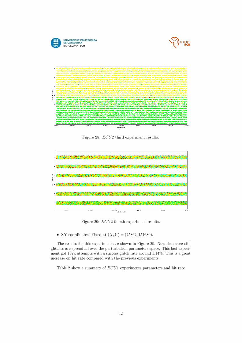
Figure 28: ECU2 third experiment results.
Figure 29: ECU2 fourth experiment results.
• XY coordinates: Fixed at (X,Y ) = (25862, 151680).
The results for this experiment are shown in Figure 29. Now the successfulglitches are spread all over the perturbation parameters space. This last experi-ment got 137k attempts with a success glitch rate around 1.14%. This is a greatincrease on hit rate compared with the previous experiments.
Table 2 show a summary of ECU1 experiments parameters and hit rate.
42
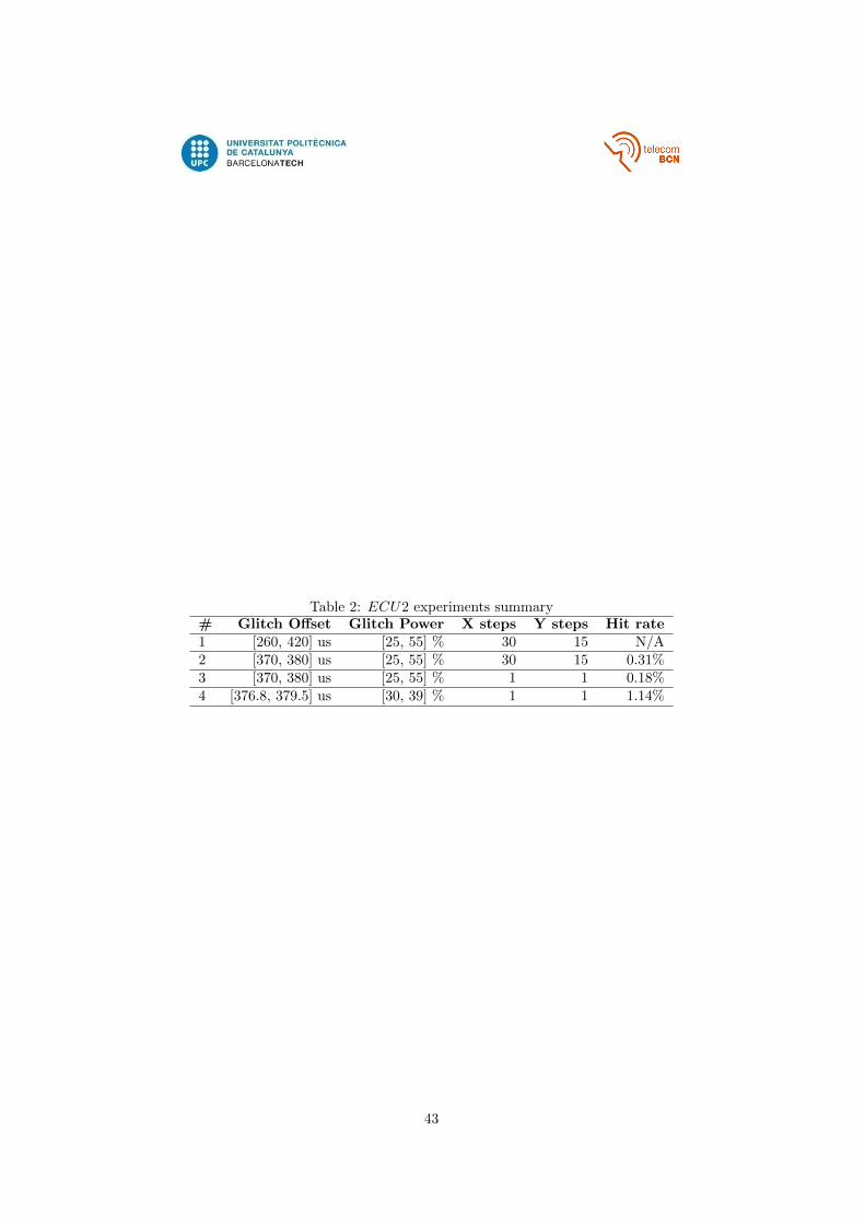
Table 2: ECU2 experiments summary# Glitch Offset Glitch Power X steps Y steps Hit rate1 [260, 420] us [25, 55] % 30 15 N/A2 [370, 380] us [25, 55] % 30 15 0.31%3 [370, 380] us [25, 55] % 1 1 0.18%4 [376.8, 379.5] us [30, 39] % 1 1 1.14%
43
4 Results
After the characterization experiments, two sets of perturbation parameterswith a high success glitch score are obtained (one for each target). These pa-rameters are applied in a final experiment for extracting the firmware.
This experiment is identical to the characterization experiments, with theonly difference that now the response from the target is logged in the com-puter in order to reconstruct the firmware binary, and the address for theReadMemoryByAddress request is incremented after each successful glitch. Thissection collects the results of the firmware extraction attacks in both targets.
4.1 ECU1
For this target, the final perturbation parameters were as follow:
• VCC Voltage: 2.3 V
• Glitch Offset: Random within 1052 µs and 1055 µs (3 µs wide)
• Glitch Voltage: Random within -0.85 V and -0.8 V
• Glitch Length: Random within 250 ns and 274 ns
The firmware downloading experiment achieved a final successful glitch scoreof about 3% after 300k attempts.
A total of 512 KB were downloaded, corresponding to the IC flash memoryaddress space (0x000000 - 0x080000). The download was made at 63 bytes persuccessful glitch, as the target device implementation of ReadMemoryByAddresswould only accept a addressAndLengthFormatIdentifier parameter value of0x14 (i.e. one byte for memorySize parameter and 4 bytes for memoryAddress
parameter, refer to Appendix A.2 for details.) and a maximum memorySize pa-rameter of 0x3F. The reasons behind this peculiar values may be related to thesecurity implications of implementing dynamic memory allocators, as a staticbuffer for the implementation must be used, according to the MISRA C guide-lines2. Moreover, the relatively small size of this static buffer may be due to thetarget RAM limitations.
Once the entire firmware binary was downloaded and reconstructed, it wasdisassembled and analyzed using IDA Pro, a commercial interactive disassem-bler. IDA performs automatic code analysis, using cross-references betweencode sections and other information. However, the process of reverse engineeran executable binary requires of human intervention, so IDA has interactivefunctionality to aid in improving the disassembly. A typical IDA user will beginwith an automatically generated disassembly listing and then convert sectionsof the binary into code or data, rename, annotate and add information to thelisting, until it becomes clear what the binary does [34].
2MISRA C is a set of guidelines and best practices for developing C code for safety-relatedapplications in critical systems. More details at https://www.misra.org.uk/Activities/
MISRAC/tabid/160/Default.aspx
44
With the help of Riscure security analysts experienced in binary reverse engi-neering it was possible to locate the routine responsible for the SecurityAccessauthentication. The algorithm used for transforming the seed into the keywas extracted, implemented in the testing computer and later verified with aSecurityAccess request. The response to that request was positive, meaningthat the correct algorithm was obtained and from now on it is possible to au-thenticate and perform more advanced requests, posing as an authorized testinguser.
4.2 ECU2
For this target, the final perturbation parameters were as follow:
• Glitch Offset: Random within 376.8 µs and 379.5 µs (2.7 µs wide)
• Glitch Power: Random within 30% and 39% of EM probe maximum power
• XY coordinates: Fixed at (X,Y ) = (25862, 151680).
The firmware downloading experiment achieved a final successful glitch scoreof about 1.7% after 500k attempts.
This target ReadMemoryByAddress implementation was more flexible, al-lowing a addressAndLengthFormatIdentifier parameter value of 0x23 andan arbitrary value for memorySize parameter. There was an attempt of settinga value for memorySize parameter to 0xFFFF but with such a big value the per-turbation parameters were no longer adequate and any successful glitch was ob-tained, most probably due to a change in the request handler timing introducedby such a big memorySize parameter. After some tries, memorySize parameterwas set to 0x01FF, obtaining 511 bytes per successful glitch. According to ICmanufacturer website the target has 3 MB of flash memory, and the experi-ment downloaded its entire memory address space (0x000000 - 0x300000). Itis worth mentioning that this address space is determined by an educated guess,since no datasheet is available for this target.
The resulting binary firmware was also disassembled and analyzed using IDAPro. Some efforts in finding the SecurityAccess authentication routine weremade without success. The big size of the binary makes the analysis tediousand time consuming, and it is left for future work. Even without finding therequired authentication algorithm, the device is to be considered compromised,as the firmware is already extracted.
45
5 Conclusions and Future Work
The present work has shown that, without the proper countermeasures, a givenECU could be target of a non-invasive, active side channel attack and be com-promised with relative easiness.
As shown in Section 4, both targets were compromised extracting the run-ning firmware by means of fault injection techniques. Section 1 describes therisks and possible consequences that could follow to an attack such as the per-formed in the present work. Moreover, Section 4.1 shows that the analysis of theextracted firmware running in ECU1 allowed to obtain the needed credentialsthat give security access to the device, in a way that fault injection is no longerneeded. This makes the rest of threats easier to accomplish, as an attacker couldpatch the firmware safely using UDS services such as WriteMemoryByAddress
or RequestDownload and run arbitrary code in the device.
5.1 Countermeasures
For protecting the devices against fault injection attacks, there exist counter-measures that makes a fault injection attack much harder or even unfeasible.These countermeasures can be built in hardware or implemented in software.When any of the countermeasures detect a fault injection attempt, a reactionis to be made, usually a hardware reset or a interruption that triggers otheractions.
5.1.1 Hardware
There are many ways to protect a circuit against fault injection techniques,active and passive protections [35]. Some active protection examples are thefollowing:
• Supply voltage detectors: react to abrupt variations in the applied poten-tial and continuously ascertain that voltage is within the circuit tolerancethresholds, to detect voltage glitching.
• Hardware redundancy: redundancy of hardware blocks (or a single blockprocessing the operation multiple times) followed by a test by a compara-tor. When different results don’t match, a reaction is made.
• Light detectors: detect changes in the gradient of light, in order to detectoptical fault injection attacks.
• Frequency detectors: impose an interval of operation outside which theelectronic circuit will reset itself, to detect clock glitching.
• Active shields: metal meshes that cover the entire chip and has data pass-ing continuously in them. If there is a disconnection or modification of thismesh the chip will not operate anymore. This is primarily a countermea-sure against probing, although it helps protecting against fault injectionas it makes the location of specific blocks in a circuit harder
46
The second class of hardware protection mechanisms consists of passive pro-tections that increase the difficulty of successfully attacking a device:
• Mechanisms that introduce dummy random cycles (i.e. random delays)during code processing. This effectively causes jitter, making triggeringand obtaining timing perturbation parameters much harder.
• Passive shield: a full metal layer covers some sensitive chip parts, whichmakes light or electromagnetic pulse attacks more difficult as the shieldneeds to be removed before the attack can proceed.
• Unstable internal frequency generators: protect against attacks that needto be synchronized with a certain event, as events occur at different mo-ments in different executions generating again artificial jitter.
5.1.2 Software
This countermeasures are implemented when hardware countermeasures are in-sufficient or as cautious protection against future attack techniques that mightdefeat present-generation hardware countermeasures. The advantage of softwarecountermeasures is that they do not increase the hardware block size, althoughthey do impact the protected functions’ execution time. Some examples of soft-ware countermeasures are the following:
• Checksums and integrity checks: this mechanisms can be implementedin software, often complementary to hardware checksums. Software CRCscan be applied to buffers of data (sometimes fragmented over various phys-ical addresses) rather than machine words.
• Software redundancy: as hardware redundancy, it consists in performingthe same operations several times and comparing the results to verifythat the correct result is generated. This redundancy is more secure if thefollowing calculations are different (e.g. encrypt-decrypt-encrypt, sign-verify) than the first so that the same fault cannot be used at differenttimes. Also, it is desirable to limit compiler optimizations, as sometimesredundant source code is optimized by them.
• Use non-trivial values for constant values if possible, preferably with maxi-mal hamming distance. Boolean and simple data values are easy to manip-ulate, as bit flipping is one of the most common effects of fault injection.This reduces the chances of matching a non trivial value using FI.
5.2 Future work
This work leaves several open questions that are interesting for future work:
• Perform similar experiments with newer ECUs (late 2016 or later) andassess the security of modern automotive systems using fault injectiontechniques, specially if the MCU built in the targets has ASIL-D certifi-cation [1].
47

• Continue with the extracted firmware analysis. Reverse engineering theextracted binaries could reveal additional security vulnerabilities that couldbe used to compromise the targets without using FI. Additionally, thesevulnerabilities need to be evaluated in case that they can be used for at-tack escalation, i.e. extending the attack from the compromised target toothers devices in the same network.
48
A ISO 14229: Unified Diagnostic Services (UDS)
ISO 14229 specifies data link independent requirements of diagnostic services,which allow a diagnostic tester (client) to control diagnostic functions in anon-vehicle Electronic Control Unit (server) such as an electronic fuel injection,automatic gear box, anti-lock braking system, etc. connected on a serial datalink embedded in a road vehicle. It also specifies generic services which al-low the diagnostic tester (client) to stop or to resume non-diagnostic messagetransmission on the data link. ISO 14229 does not, by itself, specify any imple-mentation requirements [36]. Nevertheless, the target ECUs mentioned in thepresent work follow the ISO 14229-3 implementation requirements. These spec-ifications, known as UDSonCAN, detail the implementation of a common set ofunified diagnostic services (UDS), in accordance with ISO 14229, on controllerarea networks (CAN) as specified in ISO 11898 [37].
This standard describes, among other specifications and requirements, a setof diagnostic services to perform functions such as test, inspection, monitoringor diagnosis of on-board vehicle servers. The client uses these services to re-quest diagnostic functions to be performed in one or more servers. The server,usually a function that is part of an ECU, uses the services to send responsedata, provided by the requested diagnostic service, back to the client.
In the situation that a request is not valid (e.g. bad request format, unau-thorized client or service not supported) the server answers with a negativeresponse, containing a Negative Response Code (NRC). Table 3 defines some ofthe most common negative response codes used within ISO 14229. More NRCsexist in the specification [36], but are not included in the table for the sake ofbrevity. Each diagnostic service specifies applicable negative response codes butthe diagnostic service implementation in the server may also use additional andapplicable negative response codes specified in the standard.
Table 4 collects the Service ID and description for all the services found inthe targets used for this work. More services exist in the ISO 14229 specification[36], but are not included in the table for the sake of brevity.
A.1 DiagnosticSessionControl
The DiagnosticSessionControl service is used to enable different diagnostic ses-sions in the server. A diagnostic session enables a specific set of diagnosticservices and/or functionality in the server. There shall always be exactly onediagnostic session active in a server. A server shall always start the default di-agnostic session when powered up. If no other diagnostic session is started, thenthe default diagnostic session shall be running as long as the server is powered.Any non-defaultSession is tied to a diagnostic session timer that has to be keptactive by the client using the service TesterPresent.
Figure 30 shows the service request format definition. More details can befound in Section 9.2 of [36].
49
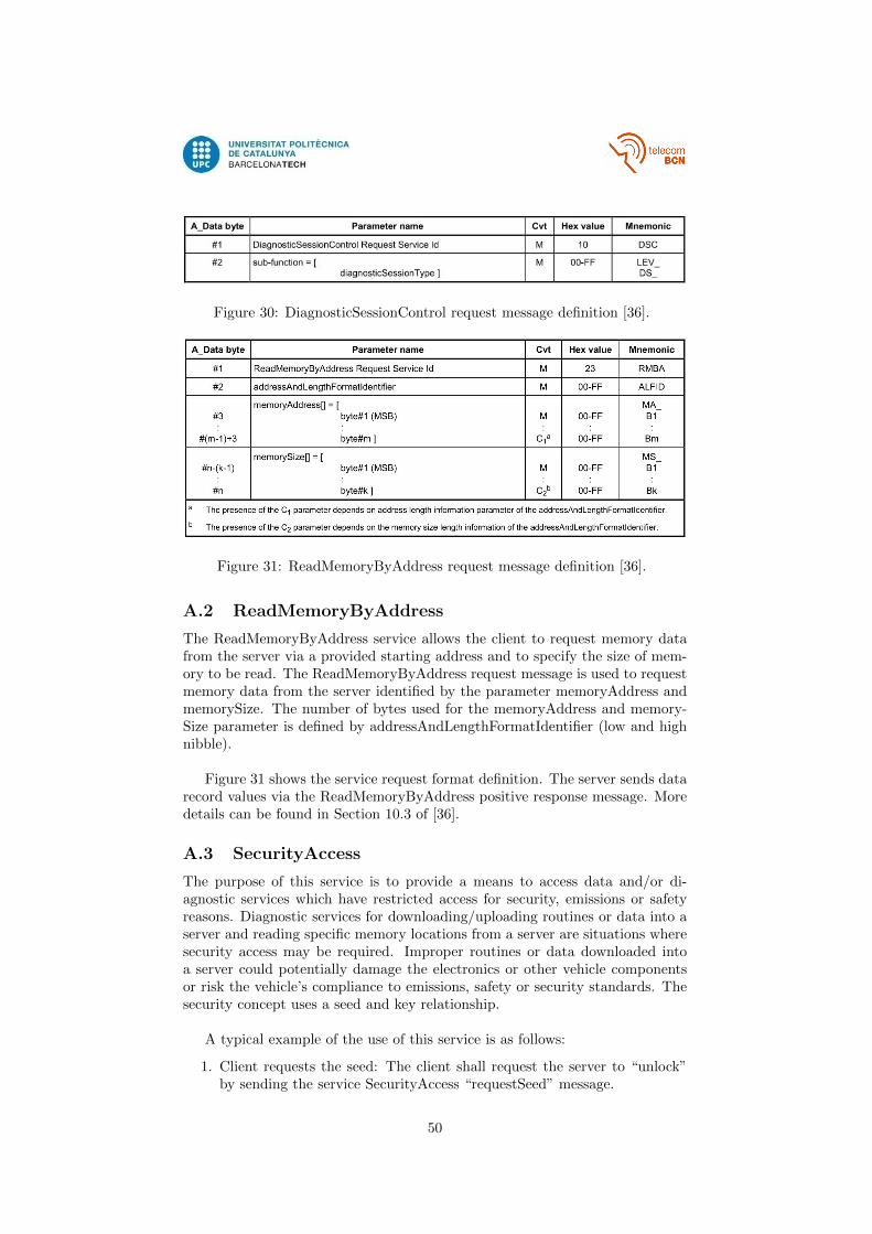
Figure 30: DiagnosticSessionControl request message definition [36].
Figure 31: ReadMemoryByAddress request message definition [36].
A.2 ReadMemoryByAddress
The ReadMemoryByAddress service allows the client to request memory datafrom the server via a provided starting address and to specify the size of mem-ory to be read. The ReadMemoryByAddress request message is used to requestmemory data from the server identified by the parameter memoryAddress andmemorySize. The number of bytes used for the memoryAddress and memory-Size parameter is defined by addressAndLengthFormatIdentifier (low and highnibble).
Figure 31 shows the service request format definition. The server sends datarecord values via the ReadMemoryByAddress positive response message. Moredetails can be found in Section 10.3 of [36].
A.3 SecurityAccess
The purpose of this service is to provide a means to access data and/or di-agnostic services which have restricted access for security, emissions or safetyreasons. Diagnostic services for downloading/uploading routines or data into aserver and reading specific memory locations from a server are situations wheresecurity access may be required. Improper routines or data downloaded intoa server could potentially damage the electronics or other vehicle componentsor risk the vehicle’s compliance to emissions, safety or security standards. Thesecurity concept uses a seed and key relationship.
A typical example of the use of this service is as follows:
1. Client requests the seed: The client shall request the server to “unlock”by sending the service SecurityAccess “requestSeed” message.
50
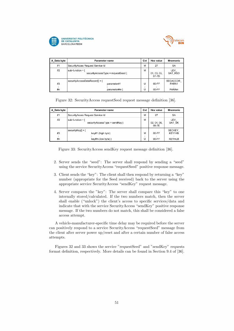
Figure 32: SecurityAccess requestSeed request message definition [36].
Figure 33: SecurityAccess sendKey request message definition [36].
2. Server sends the “seed”: The server shall respond by sending a “seed”using the service SecurityAccess “requestSeed” positive response message.
3. Client sends the “key”: The client shall then respond by returning a “key”number (appropriate for the Seed received) back to the server using theappropriate service SecurityAccess “sendKey” request message.
4. Server compares the ”key”: The server shall compare this “key” to oneinternally stored/calculated. If the two numbers match, then the servershall enable (“unlock”) the client’s access to specific services/data andindicate that with the service SecurityAccess “sendKey” positive responsemessage. If the two numbers do not match, this shall be considered a falseaccess attempt.
A vehicle-manufacturer-specific time delay may be required before the servercan positively respond to a service SecurityAccess “requestSeed” message fromthe client after server power up/reset and after a certain number of false accessattempts.
Figures 32 and 33 shows the service ”requestSeed” and ”sendKey” requestsformat definition, respectively. More details can be found in Section 9.4 of [36].
51
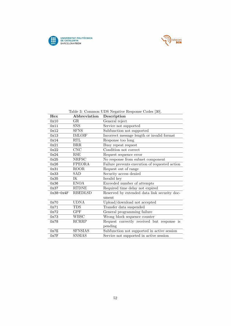
Table 3: Common UDS Negative Response Codes [30].Hex Abbreviation Description0x10 GR General reject0x11 SNS Service not supported0x12 SFNS Subfunction not supported0x13 IMLOIF Incorrect message length or invalid format0x14 RTL Response too long0x21 BRR Busy repeat request0x22 CNC Condition not correct0x24 RSE Request sequence error0x25 NRFSC No response from subnet component0x26 FPEORA Failure prevents execution of requested action0x31 ROOR Request out of range0x33 SAD Security access denied0x35 IK Invalid key0x36 ENOA Exceeded number of attempts0x37 RTDNE Required time delay not expired0x38-0x4F RBEDLSD Reserved by extended data link security doc-
ument0x70 UDNA Upload/download not accepted0x71 TDS Transfer data suspended0x72 GPF General programming failure0x73 WBSC Wrong block sequence counter0x78 RCRRP Request correctly received but response is
pending0x7E SFNSIAS Subfunction not supported in active session0x7F SNSIAS Service not supported in active session
52
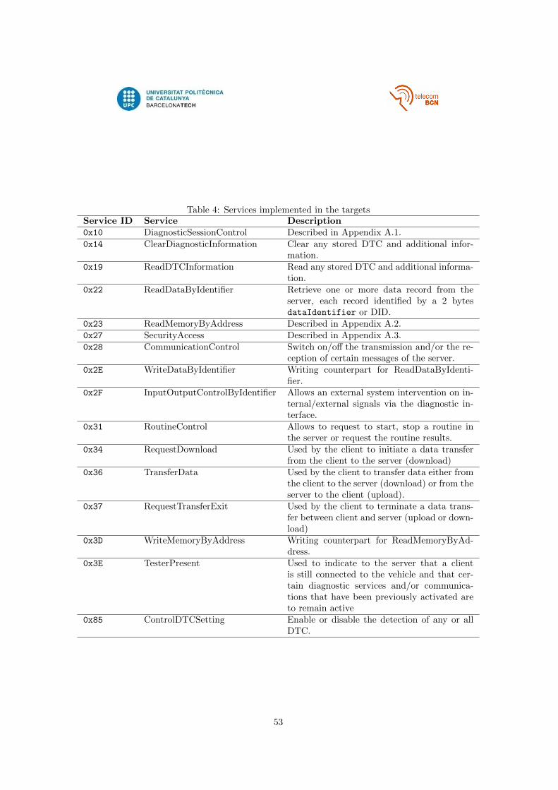
Table 4: Services implemented in the targetsService ID Service Description0x10 DiagnosticSessionControl Described in Appendix A.1.0x14 ClearDiagnosticInformation Clear any stored DTC and additional infor-
mation.0x19 ReadDTCInformation Read any stored DTC and additional informa-
tion.0x22 ReadDataByIdentifier Retrieve one or more data record from the
server, each record identified by a 2 bytesdataIdentifier or DID.
0x23 ReadMemoryByAddress Described in Appendix A.2.0x27 SecurityAccess Described in Appendix A.3.0x28 CommunicationControl Switch on/off the transmission and/or the re-
ception of certain messages of the server.0x2E WriteDataByIdentifier Writing counterpart for ReadDataByIdenti-
fier.0x2F InputOutputControlByIdentifier Allows an external system intervention on in-
ternal/external signals via the diagnostic in-terface.
0x31 RoutineControl Allows to request to start, stop a routine inthe server or request the routine results.
0x34 RequestDownload Used by the client to initiate a data transferfrom the client to the server (download)
0x36 TransferData Used by the client to transfer data either fromthe client to the server (download) or from theserver to the client (upload).
0x37 RequestTransferExit Used by the client to terminate a data trans-fer between client and server (upload or down-load)
0x3D WriteMemoryByAddress Writing counterpart for ReadMemoryByAd-dress.
0x3E TesterPresent Used to indicate to the server that a clientis still connected to the vehicle and that cer-tain diagnostic services and/or communica-tions that have been previously activated areto remain active
0x85 ControlDTCSetting Enable or disable the detection of any or allDTC.
53
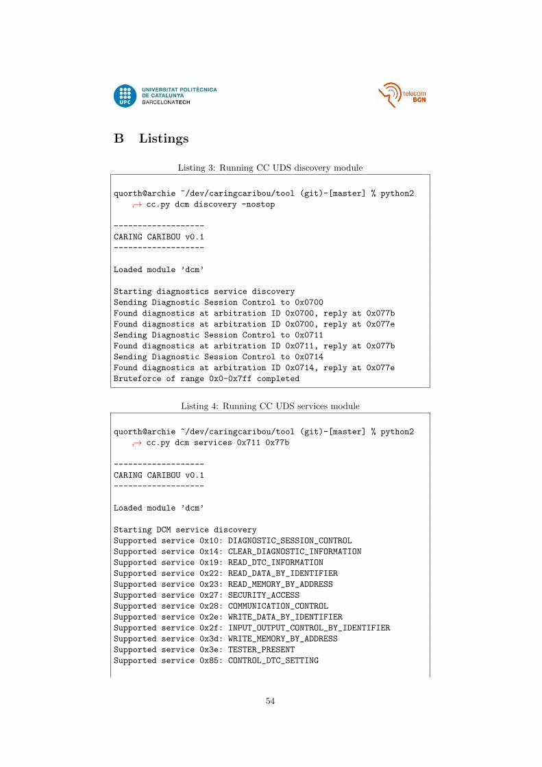
B Listings
Listing 3: Running CC UDS discovery module
quorth@archie ~/dev/caringcaribou/tool (git)-[master] % python2
↪→ cc.py dcm discovery -nostop
-------------------
CARING CARIBOU v0.1
-------------------
Loaded module ’dcm’
Starting diagnostics service discovery
Sending Diagnostic Session Control to 0x0700
Found diagnostics at arbitration ID 0x0700, reply at 0x077b
Found diagnostics at arbitration ID 0x0700, reply at 0x077e
Sending Diagnostic Session Control to 0x0711
Found diagnostics at arbitration ID 0x0711, reply at 0x077b
Sending Diagnostic Session Control to 0x0714
Found diagnostics at arbitration ID 0x0714, reply at 0x077e
Bruteforce of range 0x0-0x7ff completed
Listing 4: Running CC UDS services module
quorth@archie ~/dev/caringcaribou/tool (git)-[master] % python2
↪→ cc.py dcm services 0x711 0x77b
-------------------
CARING CARIBOU v0.1
-------------------
Loaded module ’dcm’
Starting DCM service discovery
Supported service 0x10: DIAGNOSTIC_SESSION_CONTROL
Supported service 0x14: CLEAR_DIAGNOSTIC_INFORMATION
Supported service 0x19: READ_DTC_INFORMATION
Supported service 0x22: READ_DATA_BY_IDENTIFIER
Supported service 0x23: READ_MEMORY_BY_ADDRESS
Supported service 0x27: SECURITY_ACCESS
Supported service 0x28: COMMUNICATION_CONTROL
Supported service 0x2e: WRITE_DATA_BY_IDENTIFIER
Supported service 0x2f: INPUT_OUTPUT_CONTROL_BY_IDENTIFIER
Supported service 0x3d: WRITE_MEMORY_BY_ADDRESS
Supported service 0x3e: TESTER_PRESENT
Supported service 0x85: CONTROL_DTC_SETTING
54
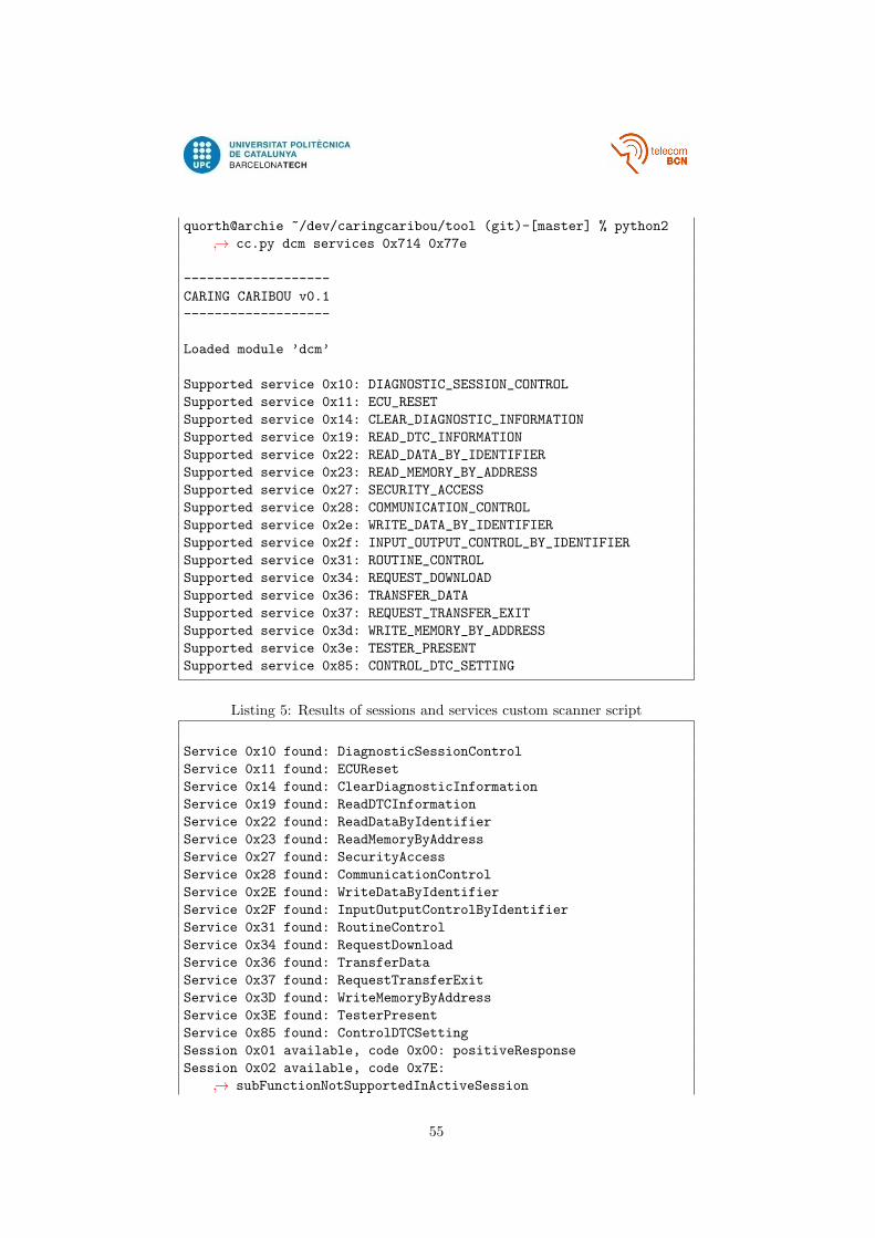
quorth@archie ~/dev/caringcaribou/tool (git)-[master] % python2
↪→ cc.py dcm services 0x714 0x77e
-------------------
CARING CARIBOU v0.1
-------------------
Loaded module ’dcm’
Supported service 0x10: DIAGNOSTIC_SESSION_CONTROL
Supported service 0x11: ECU_RESET
Supported service 0x14: CLEAR_DIAGNOSTIC_INFORMATION
Supported service 0x19: READ_DTC_INFORMATION
Supported service 0x22: READ_DATA_BY_IDENTIFIER
Supported service 0x23: READ_MEMORY_BY_ADDRESS
Supported service 0x27: SECURITY_ACCESS
Supported service 0x28: COMMUNICATION_CONTROL
Supported service 0x2e: WRITE_DATA_BY_IDENTIFIER
Supported service 0x2f: INPUT_OUTPUT_CONTROL_BY_IDENTIFIER
Supported service 0x31: ROUTINE_CONTROL
Supported service 0x34: REQUEST_DOWNLOAD
Supported service 0x36: TRANSFER_DATA
Supported service 0x37: REQUEST_TRANSFER_EXIT
Supported service 0x3d: WRITE_MEMORY_BY_ADDRESS
Supported service 0x3e: TESTER_PRESENT
Supported service 0x85: CONTROL_DTC_SETTING
Listing 5: Results of sessions and services custom scanner script
Service 0x10 found: DiagnosticSessionControl
Service 0x11 found: ECUReset
Service 0x14 found: ClearDiagnosticInformation
Service 0x19 found: ReadDTCInformation
Service 0x22 found: ReadDataByIdentifier
Service 0x23 found: ReadMemoryByAddress
Service 0x27 found: SecurityAccess
Service 0x28 found: CommunicationControl
Service 0x2E found: WriteDataByIdentifier
Service 0x2F found: InputOutputControlByIdentifier
Service 0x31 found: RoutineControl
Service 0x34 found: RequestDownload
Service 0x36 found: TransferData
Service 0x37 found: RequestTransferExit
Service 0x3D found: WriteMemoryByAddress
Service 0x3E found: TesterPresent
Service 0x85 found: ControlDTCSetting
Session 0x01 available, code 0x00: positiveResponse
Session 0x02 available, code 0x7E:
↪→ subFunctionNotSupportedInActiveSession
55
Session 0x03 available, code 0x00: positiveResponse
Session 0x40 available, code 0x00: positiveResponse
Session 0x4F available, code 0x00: positiveResponse
Session 0x60 available, code 0x00: positiveResponse
(!!) Timeout in session 0x81
Session 0x82 available, code 0x7E:
↪→ subFunctionNotSupportedInActiveSession
(!!) Timeout in session 0x83
(!!) Timeout in session 0xC0
(!!) Timeout in session 0xCF
(!!) Timeout in session 0xE0
Evaluating available services in session 0x01
Service 0x10 (DiagnosticSessionControl) positive response
Service 0x11 (ECUReset) response 0x12:
↪→ subFunctionNotSupported
Service 0x14 (ClearDiagnosticInformation) response 0x31:
↪→ requestOutOfRange
Service 0x19 (ReadDTCInformation) response 0x13:
↪→ incorrectMessageLengthOrInvalidFormat
(!!) Timeout in serviceTry 0x22 (ReadDataByIdentifier)
Service 0x23 (ReadMemoryByAddress) response 0x7F:
↪→ serviceNotSupportedInActiveSession
Service 0x27 (SecurityAccess) response 0x7F:
↪→ serviceNotSupportedInActiveSession
Service 0x28 (CommunicationControl) response 0x7F:
↪→ serviceNotSupportedInActiveSession
Service 0x2E (WriteDataByIdentifier) response 0x31:
↪→ requestOutOfRange
Service 0x2F (InputOutputControlByIdentifier) response 0
↪→ x13: incorrectMessageLengthOrInvalidFormat
Service 0x31 (RoutineControl) response 0x13:
↪→ incorrectMessageLengthOrInvalidFormat
Service 0x34 (RequestDownload) response 0x7F:
↪→ serviceNotSupportedInActiveSession
Service 0x36 (TransferData) response 0x7F:
↪→ serviceNotSupportedInActiveSession
Service 0x37 (RequestTransferExit) response 0x7F:
↪→ serviceNotSupportedInActiveSession
Service 0x3D (WriteMemoryByAddress) response 0x7F:
↪→ serviceNotSupportedInActiveSession
(!!) Timeout in serviceTry 0x3E (TesterPresent)
Service 0x85 (ControlDTCSetting) response 0x7F:
↪→ serviceNotSupportedInActiveSession
Evaluating available services in session 0x02
Not able to enter to session 0x02 from extendedDiagnosticSession,
↪→ received code 0x78 (responsePending), skipping...
Evaluating available services in session 0x03
Service 0x10 (DiagnosticSessionControl) positive response
Service 0x11 (ECUReset) response 0x12:
↪→ subFunctionNotSupported
56
Service 0x14 (ClearDiagnosticInformation) response 0x31:
↪→ requestOutOfRange
Service 0x19 (ReadDTCInformation) response 0x13:
↪→ incorrectMessageLengthOrInvalidFormat
(!!) Timeout in serviceTry 0x22 (ReadDataByIdentifier)
Service 0x23 (ReadMemoryByAddress) response 0x7F:
↪→ serviceNotSupportedInActiveSession
Service 0x27 (SecurityAccess) response 0x12:
↪→ subFunctionNotSupported
Service 0x28 (CommunicationControl) response 0x31:
↪→ requestOutOfRange
Service 0x2E (WriteDataByIdentifier) response 0x31:
↪→ requestOutOfRange
Service 0x2F (InputOutputControlByIdentifier) response 0
↪→ x13: incorrectMessageLengthOrInvalidFormat
Service 0x31 (RoutineControl) response 0x13:
↪→ incorrectMessageLengthOrInvalidFormat
Service 0x34 (RequestDownload) response 0x7F:
↪→ serviceNotSupportedInActiveSession
Service 0x36 (TransferData) response 0x7F:
↪→ serviceNotSupportedInActiveSession
Service 0x37 (RequestTransferExit) response 0x7F:
↪→ serviceNotSupportedInActiveSession
Service 0x3D (WriteMemoryByAddress) response 0x7F:
↪→ serviceNotSupportedInActiveSession
(!!) Timeout in serviceTry 0x3E (TesterPresent)
Service 0x85 (ControlDTCSetting) response 0x13:
↪→ incorrectMessageLengthOrInvalidFormat
Evaluating available services in session 0x40
Service 0x10 (DiagnosticSessionControl) positive response
Service 0x11 (ECUReset) response 0x12:
↪→ subFunctionNotSupported
Service 0x14 (ClearDiagnosticInformation) response 0x31:
↪→ requestOutOfRange
Service 0x19 (ReadDTCInformation) response 0x13:
↪→ incorrectMessageLengthOrInvalidFormat
(!!) Timeout in serviceTry 0x22 (ReadDataByIdentifier)
Service 0x23 (ReadMemoryByAddress) response 0x7F:
↪→ serviceNotSupportedInActiveSession
Service 0x27 (SecurityAccess) response 0x12:
↪→ subFunctionNotSupported
Service 0x28 (CommunicationControl) response 0x31:
↪→ requestOutOfRange
Service 0x2E (WriteDataByIdentifier) response 0x31:
↪→ requestOutOfRange
Service 0x2F (InputOutputControlByIdentifier) response 0
↪→ x13: incorrectMessageLengthOrInvalidFormat
Service 0x31 (RoutineControl) response 0x13:
↪→ incorrectMessageLengthOrInvalidFormat
Service 0x34 (RequestDownload) response 0x13:
57
↪→ incorrectMessageLengthOrInvalidFormat
Service 0x36 (TransferData) response 0x33:
↪→ securityAccessDenied
Service 0x37 (RequestTransferExit) response 0x33:
↪→ securityAccessDenied
Service 0x3D (WriteMemoryByAddress) response 0x7F:
↪→ serviceNotSupportedInActiveSession
(!!) Timeout in serviceTry 0x3E (TesterPresent)
Service 0x85 (ControlDTCSetting) response 0x13:
↪→ incorrectMessageLengthOrInvalidFormat
Evaluating available services in session 0x4F
Service 0x10 (DiagnosticSessionControl) positive response
Service 0x11 (ECUReset) response 0x12:
↪→ subFunctionNotSupported
Service 0x14 (ClearDiagnosticInformation) response 0x31:
↪→ requestOutOfRange
Service 0x19 (ReadDTCInformation) response 0x13:
↪→ incorrectMessageLengthOrInvalidFormat
(!!) Timeout in serviceTry 0x22 (ReadDataByIdentifier)
Service 0x23 (ReadMemoryByAddress) response 0x13:
↪→ incorrectMessageLengthOrInvalidFormat
Service 0x27 (SecurityAccess) response 0x12:
↪→ subFunctionNotSupported
Service 0x28 (CommunicationControl) response 0x31:
↪→ requestOutOfRange
Service 0x2E (WriteDataByIdentifier) response 0x31:
↪→ requestOutOfRange
Service 0x2F (InputOutputControlByIdentifier) response 0
↪→ x13: incorrectMessageLengthOrInvalidFormat
Service 0x31 (RoutineControl) response 0x13:
↪→ incorrectMessageLengthOrInvalidFormat
Service 0x34 (RequestDownload) response 0x13:
↪→ incorrectMessageLengthOrInvalidFormat
Service 0x36 (TransferData) response 0x33:
↪→ securityAccessDenied
Service 0x37 (RequestTransferExit) response 0x33:
↪→ securityAccessDenied
Service 0x3D (WriteMemoryByAddress) response 0x13:
↪→ incorrectMessageLengthOrInvalidFormat
(!!) Timeout in serviceTry 0x3E (TesterPresent)
Service 0x85 (ControlDTCSetting) response 0x13:
↪→ incorrectMessageLengthOrInvalidFormat
Evaluating available services in session 0x60
Service 0x10 (DiagnosticSessionControl) positive response
Service 0x11 (ECUReset) response 0x12:
↪→ subFunctionNotSupported
Service 0x14 (ClearDiagnosticInformation) response 0x31:
↪→ requestOutOfRange
Service 0x19 (ReadDTCInformation) response 0x13:
↪→ incorrectMessageLengthOrInvalidFormat
58
(!!) Timeout in serviceTry 0x22 (ReadDataByIdentifier)
Service 0x23 (ReadMemoryByAddress) response 0x13:
↪→ incorrectMessageLengthOrInvalidFormat
Service 0x27 (SecurityAccess) response 0x12:
↪→ subFunctionNotSupported
Service 0x28 (CommunicationControl) response 0x31:
↪→ requestOutOfRange
Service 0x2E (WriteDataByIdentifier) response 0x31:
↪→ requestOutOfRange
Service 0x2F (InputOutputControlByIdentifier) response 0
↪→ x13: incorrectMessageLengthOrInvalidFormat
Service 0x31 (RoutineControl) response 0x13:
↪→ incorrectMessageLengthOrInvalidFormat
Service 0x34 (RequestDownload) response 0x13:
↪→ incorrectMessageLengthOrInvalidFormat
Service 0x36 (TransferData) response 0x33:
↪→ securityAccessDenied
Service 0x37 (RequestTransferExit) response 0x33:
↪→ securityAccessDenied
Service 0x3D (WriteMemoryByAddress) response 0x13:
↪→ incorrectMessageLengthOrInvalidFormat
(!!) Timeout in serviceTry 0x3E (TesterPresent)
Service 0x85 (ControlDTCSetting) response 0x13:
↪→ incorrectMessageLengthOrInvalidFormat
Evaluating available services in session 0x82
Not able to enter to session 0x82 from extendedDiagnosticSession,
↪→ received code 0x78 (responsePending), skipping...
59
Acronyms
ALU Arithmetic Logic Unit.
ASIL Automotive Safety Integrity Level.
CAN Controller Area Network.
CRC Cyclic Redundancy Check.
DSO Digital Signal Oscilloscope.
DTC Diagnostic Trouble Code.
ECU Electronic Control Unit.
EMFI ElectroMagnetic Fault Injection.
FI Fault Injection.
GPIO General Purpose Input/Output.
IC Integrated Circuit.
MCU MicroController Unit.
NRC Negative Response Code.
PCB Printed Circuit Board.
RTOS Real Time Operating System.
SCA Side Channel Analysis.
SoC System on Chip.
UART Universal Asynchronous Receiver-Transmitter.
UDS Unified Diagnostic Services.
60
References
[1] Nils Wiersma and Ramiro Pareja. Safety != security: On the resilience ofASIL-D certified microcontrollers against fault injection attacks. In 2017Workshop on Fault Diagnosis and Tolerance in Cryptography (FDTC),pages 9–16. IEEE, 2017.
[2] Paul C. Kocher, Joshua Jaffe, and Benjamin Jun. Differential power analy-sis. In Proceedings of the 19th Annual International Cryptology Conferenceon Advances in Cryptology, CRYPTO ’99, pages 388–397, London, UK,1999. Springer-Verlag.
[3] Stefan Mangard, Elisabeth Oswald, and Thomas Popp. Power analysisattacks: Revealing the secrets of smart cards. Springer Publishing Company,Incorporated, 2010.
[4] Baris Ege. Physical Security Analysis of Embedded Devices. PhD thesis,Radboud University Nijmegen, 2016.
[5] Michel Agoyan, Jean-Max Dutertre, David Naccache, Bruno Robisson,and Assia Tria. When clocks fail: On critical paths and clock faults. InCARDIS, volume 10, pages 182–193. Springer, 2010.
[6] Thomas Korak and Michael Hoefler. On the effects of clock and powersupply tampering on two microcontroller platforms. In Fault Diagnosisand Tolerance in Cryptography (FDTC), 2014 Workshop on, pages 8–17.IEEE, 2014.
[7] Josep Balasch, Benedikt Gierlichs, and Ingrid Verbauwhede. An in-depthand black-box characterization of the effects of clock glitches on 8-bitMCUs. In Proceedings of the 2011 Workshop on Fault Diagnosis and Tol-erance in Cryptography, FDTC ’11, pages 105–114, Washington, DC, USA,2011. IEEE Computer Society.
[8] Behzad Razavi. Fundamentals of microelectronics. Jhon Wiley india Pvt.Ltd, 2009.
[9] Loic Zussa, Jean-Max Dutertre, Jessy Clediere, and Assia Tria. Powersupply glitch induced faults on FPGA: An in-depth analysis of the injectionmechanism. In On-Line Testing Symposium (IOLTS), 2013 IEEE 19thInternational, pages 110–115. IEEE, 2013.
[10] Niek Timmers and Cristofaro Mune. Escalating privileges in linux usingvoltage fault injection. In 2017 Workshop on Fault Diagnosis and Tolerancein Cryptography (FDTC), pages 1–8. IEEE, 2017.
[11] Robert Van Spyk Rajesh Velegalati and Jasper van Woudenberg. Electromagnetic fault injection in practice. In International Cryptographic ModuleConference (ICMC), 2013.
[12] Maurice Aarts. Electromagnetic fault injection using transient pulse injec-tions. Master’s thesis, Technical University Eindhoven, 2013, 2013.
[13] Riscure B.V. EM-FI R&D report v0.5. technical report. Technical report,Riscure B.V., 2013. [Confidential/Unpublished].
61
[14] Riscure B.V. EM-FI transient probe datasheet. https://www.riscure.
com/uploads/2017/07/datasheet_em-fi_transient_probe.pdf, 2017.[Online; accessed 16 January 2018].
[15] Riscure B.V. FI training. Technical report, Riscure B.V., 2017. [Confiden-tial/Unpublished].
[16] Nicolas Moro, Amine Dehbaoui, Karine Heydemann, Bruno Robisson, andEmmanuelle Encrenaz. Electromagnetic fault injection: towards a faultmodel on a 32-bit microcontroller. In Fault Diagnosis and Tolerance inCryptography (FDTC), 2013 Workshop on, pages 77–88. IEEE, 2013.
[17] Albert Spruyt. Building fault models for microcontrollers. University ofAmsterdam, Amsterdam, 2012.
[18] Cyril Roscian, Alexandre Sarafianos, Jean-Max Dutertre, and Assia Tria.Fault model analysis of laser-induced faults in sram memory cells. In FaultDiagnosis and Tolerance in Cryptography (FDTC), 2013 Workshop on,pages 89–98. IEEE, 2013.
[19] Johannes Blomer and Jean-Pierre Seifert. Fault based cryptanalysis ofthe advanced encryption standard (AES). In Computer Aided Verification,pages 162–181. Springer, 2003.
[20] Eli Biham and Adi Shamir. Differential fault analysis of secret key cryp-tosystems. Advances in Cryptology—CRYPTO’97, pages 513–525, 1997.
[21] Ingrid Biehl, Bernd Meyer, and Volker Muller. Differential fault attacks onelliptic curve cryptosystems. In Advances in Cryptology—CRYPTO 2000,pages 131–146. Springer, 2000.
[22] Dan Boneh, Richard DeMillo, and Richard Lipton. On the importanceof checking cryptographic protocols for faults. In Advances in Cryptol-ogy—EUROCRYPT’97, pages 37–51. Springer, 1997.
[23] Jorn-Marc Schmidt and Michael Hutter. Optical and EM fault-attacks oncrt-based rsa: Concrete results. na, 2007.
[24] Niek Timmer, Albert Spruyt, and Marc Witteman. Controlling PC onARM using fault injection slides. https://www.riscure.com/uploads/
2017/09/Riscure_Controlling_PC_FDTC_slides.pdf, 2016. [Online; ac-cessed 16 January 2018].
[25] Riscure B.V. icWaves datasheet. https://www.riscure.com/uploads/
2017/06/datasheet_icwaves_3c.pdf, 2017. [Online; accessed 16 January2018].
[26] Riscure B.V. Spider datasheet. https://www.riscure.com/uploads/
2017/07/spider_datasheet_1.pdf, 2017. [Online; accessed 16 January2018].
[27] Riscure B.V. Inspector FI brochure. https://www.riscure.com/uploads/2017/07/inspector_brochure.pdf, 2017. [Online; accessed 16 January2018].
62
[28] Riscure B.V. VC-Glitcher datasheet. https://www.riscure.com/
uploads/2017/07/datasheet_vcglitcher.pdf, 2017. [Online; accessed16 January 2018].
[29] LAWICEL AB. CANUSB product webpage. http://www.can232.com/
?page_id=16, 2017. [Online; accessed 16 January 2018].
[30] Craig Smith. The Car Hacker’s Handbook : A Guide for the PenetrationTester. No Starch Press, San Francisco, CA, 2016.
[31] Caring Caribou Github repository. https://github.com/CaringCaribou/caringcaribou, 2017. [Online; accessed 16 January 2018].
[32] pyvit Github repository. https://github.com/linklayer/pyvit, 2017.[Online; accessed 16 January 2018].
[33] Eric Evenchick. An introduction to the CANardtoolkit. http://www.blackhat.com/docs/asia-15/materials/
asia-15-Evenchick-Hopping-On-The-Can-Bus-wp.pdf, 2015. [On-line; accessed 16 January 2018].
[34] Wikipedia contributors. Interactive disassembler — wikipedia, thefree encyclopedia. https://en.wikipedia.org/w/index.php?title=
Interactive_Disassembler&oldid=801058000, 2017. [Online; accessed16 January 2018].
[35] Hagai Bar-El, Hamid Choukri, David Naccache, Michael Tunstall, andClaire Whelan. The sorcerer’s apprentice guide to fault attacks. Proceedingsof the IEEE, 94(2):370–382, 2006.
[36] ISO ISO. 14229-1: 2013 Road vehicles–Unified Diagnostic services (UDS)–Part 1: Specification and requirements, 2013.
[37] ISO ISO. 14229-3: 2012 Road vehicles–Unified Diagnostic services (UDS)–Part 3: Unified diagnostic services on CAN implementation (UDSonCAN),2013.
63