Embed Size (px)
Citation preview

Section 22. Direct Memory Access (DMA)
Direct M
emory
Access (D
MA
)
22
HIGHLIGHTSThis section of the manual contains the following major topics:
22.1 Introduction .................................................................................................................. 22-222.2 DMA Registers.............................................................................................................22-422.3 DMA Block Diagram...................................................................................................22-1822.4 DMA Data Transfer ....................................................................................................22-1922.5 DMA Setup.................................................................................................................22-2122.6 DMA Operating Modes .............................................................................................. 22-2722.7 Starting DMA Transfers..............................................................................................22-5022.8 DMA Channel Arbitration and Overruns .................................................................... 22-5122.9 Debugging Support .................................................................................................... 22-5322.10 Data Write and Request Collisions ............................................................................ 22-5322.11 Operation in Power-Saving Modes ............................................................................22-5522.12 Register Map.............................................................................................................. 22-5622.13 Related Application Notes.......................................................................................... 22-5722.14 Revision History .........................................................................................................22-58
© 2011 Microchip Technology Inc. DS70348B-page 22-1

dsPIC33E/PIC24E Family Reference Manual
22.1 INTRODUCTIONThe Direct Memory Access (DMA) controller is an important subsystem in Microchip’s high-performance 16-bit Digital Signal Controller (DSC) families. This subsystem facilitates the transfer of data between the CPU and its peripheral without CPU assistance. The dsPIC33E/PIC24E DMA controller is optimized for high-performance, real-time, embedded applications where determinism and system latency are priorities.
The DMA controller transfers data between peripheral data registers and data space SRAM. The dsPIC33E/PIC24E DMA subsystem uses dual-ported SRAM memory (DPSRAM) and register structures that allow the DMA to operate across its own independent address and data buses with no impact on CPU operation. This architecture eliminates the need for cycle stealing, which halts the CPU when a higher priority DMA transfer is requested. Both the CPU and DMA controller can write and read to/from addresses within data space without interference, such as CPU stalls, resulting in maximized, real-time performance. Alternatively, DMA operation and data transfer to/from the memory and peripherals are not impacted by CPU processing. For example, when a Run-Time Self-Programming (RTSP) operation is performed, the CPU does not execute any instructions until RTSP is finished. This condition, however, does not impact data transfer to/from memory and the peripherals.
In addition, DMA can access entire data memory space (SRAM and DPSRAM). The Data Memory Bus Arbiter is utilized when either the CPU or DMA attempt to access non-dual-ported SRAM, resulting in potential DMA or CPU stalls.
Figure 22-1: DMA Controller
Note: This family reference manual section is meant to serve as a complement to device data sheets. Depending on the device variant, this manual section may not apply to all dsPIC33E/PIC24E devices.
Please consult the note at the beginning of the “Direct Memory Access (DMA)”chapter in the current device data sheet to check whether this document supports the device you are using.
Device data sheets and family reference manual sections are available for download from the Microchip Worldwide Web site at: http://www.microchip.com
DMA CPU
DPSRAM
Peripheral
Arbiter
SRAM
DS70348B-page 22-2 © 2011 Microchip Technology Inc.
Section 22. Direct Memory Access (DMA)D
irect Mem
ory A
ccess (DM
A)
22
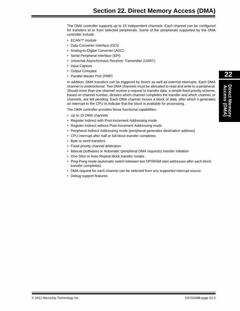
The DMA controller supports up to 15 independent channels. Each channel can be configured for transfers to or from selected peripherals. Some of the peripherals supported by the DMA controller include:
• ECAN™ module• Data Converter Interface (DCI)• Analog-to-Digital Converter (ADC)• Serial Peripheral Interface (SPI)• Universal Asynchronous Receiver Transmitter (UART)• Input Capture• Output Compare• Parallel Master Port (PMP)
In addition, DMA transfers can be triggered by timers as well as external interrupts. Each DMA channel is unidirectional. Two DMA channels must be allocated to read and write to a peripheral. Should more than one channel receive a request to transfer data, a simple fixed priority scheme, based on channel number, dictates which channel completes the transfer and which channel, or channels, are left pending. Each DMA channel moves a block of data, after which it generates an interrupt to the CPU to indicate that the block is available for processing.
The DMA controller provides these functional capabilities:
• Up to 15 DMA channels• Register Indirect with Post-Increment Addressing mode• Register Indirect without Post-Increment Addressing mode• Peripheral Indirect Addressing mode (peripheral generates destination address)• CPU interrupt after half or full-block transfer completes• Byte or word transfers• Fixed priority channel arbitration• Manual (software) or Automatic (peripheral DMA requests) transfer initiation• One-Shot or Auto-Repeat block transfer modes• Ping-Pong mode (automatic switch between two DPSRAM start addresses after each block
transfer completes)• DMA request for each channel can be selected from any supported interrupt source• Debug support features
© 2011 Microchip Technology Inc. DS70348B-page 22-3
dsPIC33E/PIC24E Family Reference Manual
22.2 DMA REGISTERSEach DMA channel has a set of six status and control registers.
• DMAxCON: DMA Channel x Control RegisterThis register configures the corresponding DMA channel by enabling/disabling the channel, specifying data transfer size, direction and block interrupt method, and selecting DMA Channel Addressing mode, Operating mode and Null Data Write mode.
• DMAxREQ: DMA Channel x IRQ Select RegisterThis register associates the DMA channel with a specific DMA capable peripheral by assigning the peripheral IRQ to the DMA channel.
• DMAxSTAH: DMA Channel x Start Address Register A (High)/DMAxSTAL: DMA Chan-nel x Start Address Register A (Low)This register specifies the primary start address of the data block to be transferred by DMA channel x to or from the DPSRAM (or RAM). Reads of this register return the value of the latest transfer address. Writes to this register while the channel x is enabled (i.e., active) may result in unpredictable behavior and should be avoided.
DMAxSTA is a 24-bit register, which is composed of two 16-bit registers, DMAxSTAH and DMAxSTAL, containing bits 23-16 and 15-0, respectively. The DMAxSTA register can only be accessed by reading and writing the DMAxSTAH and DMAxSTAL registers. However, throughout this document, the names DMAxSTA and DMAxSTAH/DMAxSTAL are used interchangeably.
• DMAxSTBH: DMA Channel x Start Address Register B (High)/DMAxSTBL: DMA Channel x Start Address Register B (Low)This register specifies the secondary start address of the data block to be transferred by DMA channel x to or from the DPSRAM (or RAM). Reads of this register return the value of the latest transfer address. Writes to this register while the channel x is enabled (i.e., active) may result in unpredictable behavior and should be avoided.
DMAxSTB is a 24-bit register, which is composed of two 16-bit registers, DMAxSTBH and DMAxSTBL, containing bits 23-16 and 15-0, respectively. The DMAxSTB register can only be accessed by reading and writing the DMAxSTBH and DMAxSTBL registers. However, throughout this document, the names DMAxSTB and DMAxSTBH/DMAxSTBL are used interchangeably.
• DMAxPAD: DMA Channel x Peripheral Address RegisterThis register contains the static address of the peripheral data register. Writes to this register while the corresponding DMA channel is enabled (i.e., active) may result in unpredictable behavior and should be avoided.
• DMAxCNT: DMA Channel x Transfer Count RegisterThis register contains the transfer count. DMAxCNT + 1 represents the number of DMA requests the channel must service before the data block transfer is considered complete. That is, a DMAxCNT value of ‘0’ will transfer one element. The value of the DMAxCNT register is independent of the transfer data size (SIZE bit in the DMAxCON register). Writes to this register while the corresponding DMA channel is enabled (i.e., active) may result in unpredictable behavior and should be avoided.
DS70348B-page 22-4 © 2011 Microchip Technology Inc.

Section 22. Direct Memory Access (DMA)D
irect Mem
ory A
ccess (DM
A)
22
In addition to the individual DMA channel registers, the DMA controller has five DMA status registers.
• DSADR: Most Recent DMA DPSRAM Address RegisterThis 16-bit, read-only, status register is common to all DMA channels. It captures the address of the most recent DPSRAM access (read or write). It is cleared at Reset and, therefore, contains the value ‘0x0000’ if read prior to any DMA activity. This register is accessible at any time but is primarily intended as a debug aid.
• DMAPWC: DMA Peripheral Write Collision Status RegisterThis 16-bit, read-only, status register is common to all DMA channels. It contains peripheral write collisions flags, PWCOLx. For detailed information, see 22.10 “Data Write and Request Collisions” for detailed information.
• DMARQC: DMA Request Collision Status RegisterThis 16-bit, read-only, status register is common to all DMA channels. It contains DMA request collision flags, RQCOLx. For detailed information, see 22.10 “Data Write and Request Collisions”.
• DMALCA: DMA Last Channel Active Status Register This 16-bit, read-only status register indicates which DMA channel was most recently active.
• DMAPPS: DMA Ping-Pong Status RegisterThis 16-bit, read-only status register provides the Ping-Pong mode status of each DMA channel by indicating which Start Address register is selected (DMAxSTA or DMAxSTB).
© 2011 Microchip Technology Inc. DS70348B-page 22-5
dsPIC33E/PIC24E Family Reference Manual
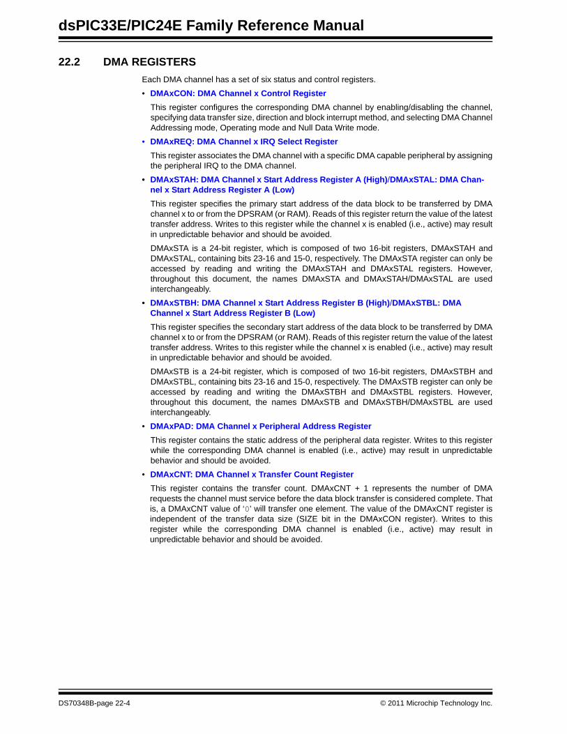
Register 22-1: DMAXCON: DMA Channel X Control Register
R/W-0 R/W-0 R/W-0 R/W-0 R/W-0 U-0 U-0 U-0CHEN SIZE DIR HALF NULLW — — —
bit 15 bit 8
U-0 U-0 R/W-0 R/W-0 U-0 U-0 R/W-0 R/W-0— — AMODE<1:0> — — MODE<1:0>
bit 7 bit 0
Legend:R = Readable bit W = Writable bit U = Unimplemented bit, read as ‘0’-n = Value at POR ‘1’ = Bit is set ‘0’ = Bit is cleared x = Bit is unknown
bit 15 CHEN: Channel Enable bit1 = Channel enabled0 = Channel disabled
bit 14 SIZE: Data Transfer Size bit1 = Byte0 = Word
bit 13 DIR: Transfer Direction bit (source/destination bus select)1 = Read from DPSRAM (or RAM) address, write to peripheral address0 = Read from Peripheral address, write to DPSRAM (or RAM) address
bit 12 HALF: Block Transfer Interrupt Select bit1 = Initiate interrupt when half of the data has been moved0 = Initiate interrupt when all of the data has been moved
bit 11 NULLW: Null Data Peripheral Write Mode Select bit1 = Null data write to peripheral in addition to DPSRAM (or RAM) write (DIR bit must also be clear)0 = Normal operation
bit 10-6 Unimplemented: Read as ‘0’bit 5-4 AMODE<1:0>: DMA Channel Addressing Mode Select bits
11 = Reserved 10 = Peripheral Indirect Addressing mode01 = Register Indirect without Post-Increment mode00 = Register Indirect with Post-Increment mode
bit 3-2 Unimplemented: Read as ‘0’bit 1-0 MODE<1:0>: DMA Channel Operating Mode Select bits
11 = One-Shot, Ping-Pong modes enabled (one block transfer from/to each DMA buffer)10 = Continuous, Ping-Pong modes enabled01 = One-Shot, Ping-Pong modes disabled00 = Continuous, Ping-Pong modes disabled
DS70348B-page 22-6 © 2011 Microchip Technology Inc.

Section 22. Direct Memory Access (DMA)D
irect Mem
ory A
ccess (DM
A)
22
Register 22-2: DMAXREQ: DMA Channel X IRQ Select Register
R/W-0 U-0 U-0 U-0 U-0 U-0 U-0 U-0FORCE(1) — — — — — — —
bit 15 bit 8
R/W-0 R/W-0 R/W-0 R/W-0 R/W-0 R/W-0 R/W-0 R/W-0IRQSEL<7:0>(2)
bit 7 bit 0
Legend:R = Readable bit W = Writable bit U = Unimplemented bit, read as ‘0’-n = Value at POR ‘1’ = Bit is set ‘0’ = Bit is cleared x = Bit is unknown
bit 15 FORCE: Force DMA Transfer bit(1)
1 = Force a single DMA transfer (manual mode)0 = Automatic DMA transfer initiation by DMA request
bit 14-8 Unimplemented: Read as ‘0’bit 7-0 IRQSEL<7:0>: DMA Peripheral IRQ Number Select bits(2)
00000000 = INT0 – External Interrupt 000000001 = IC1 – Input Capture 100000010 = OC1 – Output Compare 100000101 = IC2 – Input Capture 200000110 = OC2 – Output Compare 200000111 = TMR2 – Timer200001000 = TMR3 – Timer300001010 = SPI1 – Transfer Done00001011 = UART1RX – UART1 Receiver00001100 = UART1TX – UART1 Transmitter00001101 = ADC1 – ADC1 Convert Done00010101 = ADC2 – ADC2 Convert Done00011001 = OC3 – Output Compare 300011010 = OC4 – Output Compare 400011011 = TMR4 – Timer400011100 = TMR5 – Timer500011110 = UART2RX – UART2 Receiver00011111 = UART2TX – UART2 Transmitter00100001 = SPI2 Transfer Done00100010 = ECAN1 – RX Data Ready00100101 = IC3 – Input Capture 300100110 = IC4 – Input Capture 400101101 = PMP Data mode00110111 = ECAN2 – RX Data Ready00111100 = DCI – CODEC Transfer Done01000110 = ECAN1 – TX Data Request01000111 = ECAN2 – TX Data Request01010010 = UART3RX – UART3 Receiver01010011 = UART3TX – UART3 Transmitter01011000 = UART4RX – UART4 Receiver01011001 = UART4TX – UART4 Transmitter01011011 = SPI3 – Transfer Done01111011 = SPI4 – Transfer Done
Note 1: The FORCE bit cannot be cleared by user software. The FORCE bit is cleared by hardware when the forced DMA transfer is complete or the channel is disabled (CHEN = 0).
2: For a list of DMA-supported peripherals, refer to the specific device data sheet.
© 2011 Microchip Technology Inc. DS70348B-page 22-7
dsPIC33E/PIC24E Family Reference Manual
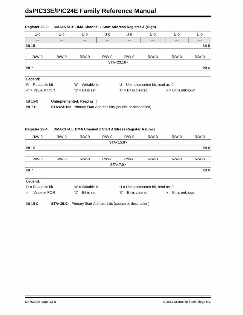
Register 22-3: DMAXSTAH: DMA Channel X Start Address Register A (High)
U-0 U-0 U-0 U-0 U-0 U-0 U-0 U-0— — — — — — — —
bit 15 bit 8
R/W-0 R/W-0 R/W-0 R/W-0 R/W-0 R/W-0 R/W-0 R/W-0STA<23:16>
bit 7 bit 0
Legend:R = Readable bit W = Writable bit U = Unimplemented bit, read as ‘0’-n = Value at POR ‘1’ = Bit is set ‘0’ = Bit is cleared x = Bit is unknown
bit 15-8 Unimplemented: Read as ‘0’bit 7-0 STA<23:16>: Primary Start Address bits (source or destination)
Register 22-4: DMAXSTAL: DMA Channel X Start Address Register A (Low)
R/W-0 R/W-0 R/W-0 R/W-0 R/W-0 R/W-0 R/W-0 R/W-0STA<15:8>
bit 15 bit 8
R/W-0 R/W-0 R/W-0 R/W-0 R/W-0 R/W-0 R/W-0 R/W-0STA<7:0>
bit 7 bit 0
Legend:R = Readable bit W = Writable bit U = Unimplemented bit, read as ‘0’-n = Value at POR ‘1’ = Bit is set ‘0’ = Bit is cleared x = Bit is unknown
bit 15-0 STA<15:0>: Primary Start Address bits (source or destination)
DS70348B-page 22-8 © 2011 Microchip Technology Inc.

Section 22. Direct Memory Access (DMA)D
irect Mem
ory A
ccess (DM
A)
22
Register 22-5: DMAXSTBH: DMA Channel X Start Address Register B (High)
U-0 U-0 U-0 U-0 U-0 U-0 U-0 U-0— — — — — — — —
bit 15 bit 8
R/W-0 R/W-0 R/W-0 R/W-0 R/W-0 R/W-0 R/W-0 R/W-0STB<23:16>
bit 7 bit 0
Legend:R = Readable bit W = Writable bit U = Unimplemented bit, read as ‘0’-n = Value at POR ‘1’ = Bit is set ‘0’ = Bit is cleared x = Bit is unknown
bit 15-8 Unimplemented: Read as ‘0’bit 7-0 STB<23:16>: Primary Start Address bits (source or destination)
Register 22-6: DMAXSTBL: DMA Channel X Start Address Register B (Low)
R/W-0 R/W-0 R/W-0 R/W-0 R/W-0 R/W-0 R/W-0 R/W-0STB<15:8>
bit 15 bit 8
R/W-0 R/W-0 R/W-0 R/W-0 R/W-0 R/W-0 R/W-0 R/W-0STB<7:0>
bit 7 bit 0
Legend:R = Readable bit W = Writable bit U = Unimplemented bit, read as ‘0’-n = Value at POR ‘1’ = Bit is set ‘0’ = Bit is cleared x = Bit is unknown
bit 15-0 STB<15:0>: Secondary Start Address Offset bits (source or destination)
© 2011 Microchip Technology Inc. DS70348B-page 22-9

dsPIC33E/PIC24E Family Reference Manual
Register 22-7: DMAXPAD: DMA Channel X Peripheral Address Register
R/W-0 R/W-0 R/W-0 R/W-0 R/W-0 R/W-0 R/W-0 R/W-0PAD<15:8>
bit 15 bit 8
R/W-0 R/W-0 R/W-0 R/W-0 R/W-0 R/W-0 R/W-0 R/W-0PAD<7:0>
bit 7 bit 0
Legend:R = Readable bit W = Writable bit U = Unimplemented bit, read as ‘0’-n = Value at POR ‘1’ = Bit is set ‘0’ = Bit is cleared x = Bit is unknown
bit 15-0 PAD<15:0>: Peripheral Address Register bits
Register 22-8: DMAXCNT: DMA Channel X Transfer Count Register
U-0 U-0 R/W-0 R/W-0 R/W-0 R/W-0 R/W-0 R/W-0— — CNT<13:8>
bit 15 bit 8
R/W-0 R/W-0 R/W-0 R/W-0 R/W-0 R/W-0 R/W-0 R/W-0CNT<7:0>
bit 7 bit 0
Legend:R = Readable bit W = Writable bit U = Unimplemented bit, read as ‘0’-n = Value at POR ‘1’ = Bit is set ‘0’ = Bit is cleared x = Bit is unknown
bit 15-14 Unimplemented: Read as ‘0’bit 13-0 CNT<13:0>: DMA Transfer Count Register bits
Register 22-9: DSADR: Most Recent DMA DPSRAM Address Register
R-0 R-0 R-0 R-0 R-0 R-0 R-0 R-0DSADR<15:8>
bit 15 bit 8
R-0 R-0 R-0 R-0 R-0 R-0 R-0 R-0DSADR<7:0>
bit 7 bit 0
Legend:R = Readable bit W = Writable bit U = Unimplemented bit, read as ‘0’-n = Value at POR ‘1’ = Bit is set ‘0’ = Bit is cleared x = Bit is unknown
bit 15-0 DSADR<15:0>: Most Recent DMA Address Accessed by DMA bits
DS70348B-page 22-10 © 2011 Microchip Technology Inc.

Section 22. Direct Memory Access (DMA)D
irect Mem
ory A
ccess (DM
A)
22
Register 22-10: DMAPWC: DMA Peripheral Write Collision Status Register
U-0 R-0 R-0 R-0 R-0 R-0 R-0 R-0— PWCOL14 PWCOL13 PWCOL12 PWCOL11 PWCOL10 PWCOL9 PWCOL8
bit 15 bit 8
R-0 R-0 R-0 R-0 R-0 R-0 R-0 R-0PWCOL7 PWCOL6 PWCOL5 PWCOL4 PWCOL3 PWCOL2 PWCOL1 PWCOL0
bit 7 bit 0
Legend:R = Readable bit W = Writable bit U = Unimplemented bit, read as ‘0’-n = Value at POR ‘1’ = Bit is set ‘0’ = Bit is cleared x = Bit is unknown
bit 15 Unimplemented: Read as ‘0’bit 14 PWCOL14: Channel 14 Peripheral Write Collision Flag bit
1 = Write collision detected0 = No write collision detected
bit 13 PWCOL13: Channel 13 Peripheral Write Collision Flag bit1 = Write collision detected0 = No write collision detected
bit 12 PWCOL12: Channel 12 Peripheral Write Collision Flag bit1 = Write collision detected0 = No write collision detected
bit 11 PWCOL11: Channel 11 Peripheral Write Collision Flag bit1 = Write collision detected0 = No write collision detected
bit 10 PWCOL10: Channel 10 Peripheral Write Collision Flag bit1 = Write collision detected0 = No write collision detected
bit 9 PWCOL9: Channel 9 Peripheral Write Collision Flag bit1 = Write collision detected0 = No write collision detected
bit 8 PWCOL8: Channel 8 Peripheral Write Collision Flag bit1 = Write collision detected0 = No write collision detected
bit 7 PWCOL7: Channel 7 Peripheral Write Collision Flag bit1 = Write collision detected0 = No write collision detected
bit 6 PWCOL6: Channel 6 Peripheral Write Collision Flag bit1 = Write collision detected0 = No write collision detected
bit 5 PWCOL5: Channel 5 Peripheral Write Collision Flag bit1 = Write collision detected0 = No write collision detected
bit 4 PWCOL4: Channel 4 Peripheral Write Collision Flag bit1 = Write collision detected0 = No write collision detected
bit 3 PWCOL3: Channel 3 Peripheral Write Collision Flag bit1 = Write collision detected0 = No write collision detected
bit 2 PWCOL2: Channel 2 Peripheral Write Collision Flag bit1 = Write collision detected0 = No write collision detected
© 2011 Microchip Technology Inc. DS70348B-page 22-11

dsPIC33E/PIC24E Family Reference Manual
bit 1 PWCOL1: Channel 1 Peripheral Write Collision Flag bit1 = Write collision detected0 = No write collision detected
bit 0 PWCOL0: Channel 0 Peripheral Write Collision Flag bit1 = Write collision detected0 = No write collision detected
Register 22-10: DMAPWC: DMA Peripheral Write Collision Status Register (Continued)
DS70348B-page 22-12 © 2011 Microchip Technology Inc.
Section 22. Direct Memory Access (DMA)D
irect Mem
ory A
ccess (DM
A)
22
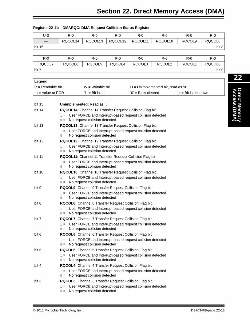
Register 22-11: DMARQC: DMA Request Collision Status Register
U-0 R-0 R-0 R-0 R-0 R-0 R-0 R-0— RQCOL14 RQCOL13 RQCOL12 RQCOL11 RQCOL10 RQCOL9 RQCOL8
bit 15 bit 8
R-0 R-0 R-0 R-0 R-0 R-0 R-0 R-0RQCOL7 RQCOL6 RQCOL5 RQCOL4 RQCOL3 RQCOL2 RQCOL1 RQCOL0
bit 7 bit 0
Legend:R = Readable bit W = Writable bit U = Unimplemented bit, read as ‘0’-n = Value at POR ‘1’ = Bit is set ‘0’ = Bit is cleared x = Bit is unknown
bit 15 Unimplemented: Read as ‘0’bit 14 RQCOL14: Channel 14 Transfer Request Collision Flag bit
1 = User FORCE and Interrupt-based request collision detected0 = No request collision detected
bit 13 RQCOL13: Channel 13 Transfer Request Collision Flag bit1 = User FORCE and Interrupt-based request collision detected0 = No request collision detected
bit 12 RQCOL12: Channel 12 Transfer Request Collision Flag bit1 = User FORCE and Interrupt-based request collision detected0 = No request collision detected
bit 11 RQCOL11: Channel 11 Transfer Request Collision Flag bit1 = User FORCE and Interrupt-based request collision detected0 = No request collision detected
bit 10 RQCOL10: Channel 10 Transfer Request Collision Flag bit1 = User FORCE and Interrupt-based request collision detected0 = No request collision detected
bit 9 RQCOL9: Channel 9 Transfer Request Collision Flag bit1 = User FORCE and Interrupt-based request collision detected0 = No request collision detected
bit 8 RQCOL8: Channel 8 Transfer Request Collision Flag bit1 = User FORCE and Interrupt-based request collision detected0 = No request collision detected
bit 7 RQCOL7: Channel 7 Transfer Request Collision Flag bit1 = User FORCE and Interrupt-based request collision detected0 = No request collision detected
bit 6 RQCOL6: Channel 6 Transfer Request Collision Flag bit1 = User FORCE and Interrupt-based request collision detected0 = No request collision detected
bit 5 RQCOL5: Channel 5 Transfer Request Collision Flag bit1 = User FORCE and Interrupt-based request collision detected0 = No request collision detected
bit 4 RQCOL4: Channel 4 Transfer Request Collision Flag bit1 = User FORCE and Interrupt-based request collision detected0 = No request collision detected
bit 3 RQCOL3: Channel 3 Transfer Request Collision Flag bit1 = User FORCE and Interrupt-based request collision detected0 = No request collision detected
© 2011 Microchip Technology Inc. DS70348B-page 22-13

dsPIC33E/PIC24E Family Reference Manual
bit 2 RQCOL2: Channel 2 Transfer Request Collision Flag bit1 = User FORCE and Interrupt-based request collision detected0 = No request collision detected
bit 1 RQCOL1: Channel 1 Transfer Request Collision Flag bit1 = User FORCE and Interrupt-based request collision detected0 = No request collision detected
bit 0 RQCOL0: Channel 0 Transfer Request Collision Flag bit1 = User FORCE and Interrupt-based request collision detected0 = No request collision detected
Register 22-11: DMARQC: DMA Request Collision Status Register (Continued)
DS70348B-page 22-14 © 2011 Microchip Technology Inc.

Section 22. Direct Memory Access (DMA)D
irect Mem
ory A
ccess (DM
A)
22
Register 22-12: DMALCA: DMA Last Channel Active Status Register
U-0 U-0 U-0 U-0 U-0 U-0 U-0 U-0— — — — — — — —
bit 15 bit 8
U-0 U-0 U-0 U-0 R-1 R-1 R-1 R-1— — — — LSTCH<3:0>
bit 7 bit 0
Legend:R = Readable bit W = Writable bit U = Unimplemented bit, read as ‘0’-n = Value at POR ‘1’ = Bit is set ‘0’ = Bit is cleared x = Bit is unknown
bit 15-4 Unimplemented: Read as ‘0’bit 3-0 LSTCH<3:0>: Last DMAC Channel Active Status bits
1111 = No DMA transfer has occurred since system Reset1110 = Last data transfer was handled by Channel 141101 = Last data transfer was handled by Channel 131100 = Last data transfer was handled by Channel 121011 = Last data transfer was handled by Channel 111010 = Last data transfer was handled by Channel 101001 = Last data transfer was handled by Channel 91000 = Last data transfer was handled by Channel 80111 = Last data transfer was handled by Channel 70110 = Last data transfer was handled by Channel 60101 = Last data transfer was handled by Channel 50100 = Last data transfer was handled by Channel 40011 = Last data transfer was handled by Channel 30010 = Last data transfer was handled by Channel 20001 = Last data transfer was handled by Channel 10000 = Last data transfer was handled by Channel 0
© 2011 Microchip Technology Inc. DS70348B-page 22-15

dsPIC33E/PIC24E Family Reference Manual
Register 22-13: DMAPPS: DMA Ping-Pong Status Register
U-0 R-0 R-0 R-0 R-0 R-0 R-0 R-0— PPST14 PPST13 PPST12 PPST11 PPST10 PPST9 PPST8
bit 15 bit 8
R-0 R-0 R-0 R-0 R-0 R-0 R-0 R-0PPST7 PPST6 PPST5 PPST4 PPST3 PPST2 PPST1 PPST0
bit 7 bit 0
Legend:R = Readable bit W = Writable bit U = Unimplemented bit, read as ‘0’-n = Value at POR ‘1’ = Bit is set ‘0’ = Bit is cleared x = Bit is unknown
bit 15 Unimplemented: Read as ‘0’bit 14 PPST14: Channel 14 Ping-Pong Mode Status Flag bit
1 = DMASTB14 register selected0 = DMASTA14 register selected
bit 13 PPST13: Channel 13 Ping-Pong Mode Status Flag bit1 = DMASTB13 register selected0 = DMASTA13 register selected
bit 12 PPST12: Channel 12 Ping-Pong Mode Status Flag bit1 = DMASTB12 register selected0 = DMASTA12 register selected
bit 11 PPST11: Channel 11 Ping-Pong Mode Status Flag bit1 = DMASTB11 register selected0 = DMASTA11 register selected
bit 10 PPST10: Channel 10 Ping-Pong Mode Status Flag bit1 = DMASTB10 register selected0 = DMASTA10 register selected
bit 9 PPST9: Channel 9 Ping-Pong Mode Status Flag bit1 = DMASTB9 register selected0 = DMASTA9 register selected
bit 8 PPST8: Channel 8 Ping-Pong Mode Status Flag bit1 = DMASTB8 register selected0 = DMASTA8 register selected
bit 7 PPST7: Channel 7 Ping-Pong Mode Status Flag bit1 = DMASTB7 register selected0 = DMASTA7 register selected
bit 6 PPST6: Channel 6 Ping-Pong Mode Status Flag bit1 = DMASTB6 register selected0 = DMASTA6 register selected
bit 5 PPST5: Channel 5 Ping-Pong Mode Status Flag bit1 = DMASTB5 register selected0 = DMASTA5 register selected
bit 4 PPST4: Channel 4 Ping-Pong Mode Status Flag bit1 = DMASTB4 register selected0 = DMASTA4 register selected
bit 3 PPST3: Channel 3 Ping-Pong Mode Status Flag bit1 = DMASTB3 register selected0 = DMASTA3 register selected
DS70348B-page 22-16 © 2011 Microchip Technology Inc.

Section 22. Direct Memory Access (DMA)D
irect Mem
ory A
ccess (DM
A)
22
bit 2 PPST2: Channel 2 Ping-Pong Mode Status Flag bit1 = DMASTB2 register selected0 = DMASTA2 register selected
bit 1 PPST1: Channel 1 Ping-Pong Mode Status Flag bit1 = DMASTB1 register selected0 = DMASTA1 register selected
bit 0 PPST0: Channel 0 Ping-Pong Mode Status Flag bit1 = DMASTB0 register selected0 = DMASTA0 register selected
Register 22-13: DMAPPS: DMA Ping-Pong Status Register (Continued)
© 2011 Microchip Technology Inc. DS70348B-page 22-17

dsPIC33E/PIC24E Family Reference Manual
22.3 DMA BLOCK DIAGRAMFigure 22-2 is a block diagram that shows how DMA integrates into the dsPIC33E/PIC24E internal architecture. The CPU communicates with conventional SRAM across the X-bus. It also communicates with Port 1 of the Dual Port SRAM (DPSRAM) block across the same X-bus. The CPU communicates with the peripherals across a separate Peripheral X-bus, which also resides within X data space.
The DMA channels communicate with Port 2 of the DPSRAM and the DMA port of each of the DMA-ready peripherals across a dedicated DMA bus.
Figure 22-2: DMA Controller Block Diagram
Unlike other architectures, the dsPIC33E/PIC24E CPU is capable of a read and a write access within each CPU bus cycle. Similarly, DMA can complete the transfer of a byte or word every bus cycle across its dedicated bus. This also ensures that all DMA transfers are not interrupted. That is, once the transfer has started, it will complete within the same cycle, regardless of other channel activity.
In addition, DMA can access the entire data memory space (SRAM and DPSRAM). The Data Memory Bus Arbiter will be utilized when either the CPU or DMA tries to access non dual-ported SRAM, which results in potential DMA or CPU stalls.
The user application can designate any DMA-ready peripheral interrupt to be a DMA request, the term given to an IRQ when it is directed to the DMA. It is assumed that when a DMA channel is configured to respond to a particular interrupt as a DMA request, the corresponding CPU interrupt is disabled, otherwise a CPU interrupt will also be requested.
Each DMA channel can also be triggered manually through software. Setting the FORCE bit in the DMAxCON register initiates a manual DMA request that is subject to the same arbitration as all interrupt-based DMA requests (see 22.8 “DMA Channel Arbitration and Overruns”).
CPU
Arbiter
DPSRAMPeripheral 1
DMA
PeripheralNon-DMA
PORT 2PORT 1
Peripheral 2
DMAReady
Peripheral 3
DMAReady
Ready
DMA X-Bus
CPU DMA
CPU DMA CPU DMA
Peripheral Indirect Address
Note: CPU and DMA address buses are not shown for clarity.
DM
AC
ontro
lDMA Controller
DMAChannels
CPU Peripheral X-Bus
IRQ to DMA and Interrupt
Controller Modules
SRAM X-Bus
IRQ to DMA and Interrupt Controller
Modules
IRQ to DMA and Interrupt Controller
Modules
0 1 2 3 N
SRAM
4 · ·
DS70348B-page 22-18 © 2011 Microchip Technology Inc.

Section 22. Direct Memory Access (DMA)D
irect Mem
ory A
ccess (DM
A)
22
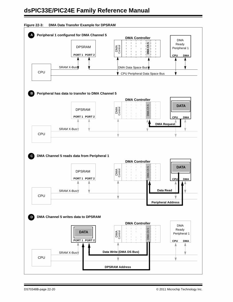
22.4 DMA DATA TRANSFERFigure 22-3 illustrates data transfer between a peripheral and the Dual Port SRAM.
A. In this example, DMA Channel 5 is configured to operate with DMA Ready Peripheral 1.B. When data is ready to be transferred from the peripheral, a DMA request is issued by the
peripheral. The DMA request is arbitrated with any other coincident requests. If this channel has the highest priority, the transfer is completed during the next cycle. Otherwise, the DMA request remains pending until it becomes the highest priority.
C. The DMA channel executes a data read from the designated peripheral address, which is user-application defined within the active channel.
D. The DMA channel writes the data to the designated DPSRAM address.
This example represents Register Indirect mode, where the DPSRAM address is designated within the DMA channel via the DMA registers (DMAxSTA or DMAxSTB). In Peripheral Indirect mode, the DPSRAM address is derived from the peripheral, not the active channel. More information on this topic is presented in 22.6.6 “Peripheral Indirect Addressing Mode”.
The entire DMA read and write transfer operation is accomplished uninterrupted in a single instruction cycle. During this entire process, a DMA request remains latched in the DMA channel until the data transfer is complete.
The DMA channel concurrently monitors the Transfer Counter register (DMA5CNT). When the transfer count reaches a user-application specified limit, data transfer is considered complete and a CPU interrupt is asserted to alert the CPU to process the newly received data.
During the data transfer cycle, the DMA controller continues to arbitrate pending or subsequent DMA requests to maximize throughput.
Data transfer between a peripheral and SRAM will be similar to the example shown in Figure 22-3; however, all access to SRAM will be gated via an arbiter, which can result in potential DMA or CPU stalls.
© 2011 Microchip Technology Inc. DS70348B-page 22-19
dsPIC33E/PIC24E Family Reference Manual
Figure 22-3: DMA Data Transfer Example for DPSRAM
CPU
DPSRAM Peripheral 1
DMA
PORT 2PORT 1
Ready
DMA Data Space Bus
CPU DMA
DM
AC
ontro
l
DMA Controller
CPU Peripheral Data Space Bus
SRAM X-Bus
DMA
Ch 5
CPU
DPSRAM Peripheral 1
DMA
PORT 2PORT 1
Ready
CPU DMAD
MA
Con
trol
DMA Controller
SRAM X-Bus
CPU
DPSRAM Peripheral 1
DMA
PORT 2PORT 1
Ready
CPU DMA
DM
AC
ontro
l
DMA Controller
SRAM X-Bus
DM
A C
h 5
CPU
DPSRAM Peripheral 1
DMA
PORT 2PORT 1
Ready
CPU DMA
DM
AC
ontro
l
DMA Controller
SRAM X-Bus
DM
A C
h 5
Peripheral 1 configured for DMA Channel 5
B
A
C
D
Peripheral has data to transfer to DMA Channel 5
DMA Channel 5 reads data from Peripheral 1
DMA Channel 5 writes data to DPSRAM
DATA
DATA
DATA
DMA Request
DM
A C
h 5
Peripheral Address
Data Read
Data Write (DMA DS Bus)
DPSRAM Address
DS70348B-page 22-20 © 2011 Microchip Technology Inc.

Section 22. Direct Memory Access (DMA)D
irect Mem
ory A
ccess (DM
A)
22
22.5 DMA SETUPFor DMA data transfer to function properly, the DMA channels and peripherals must be appropriately configured:
• DMA channels must be associated with peripherals (see 22.5.1 “DMA Channel to Peripheral Association Setup”)
• Peripherals must be properly configured (see 22.5.2 “Peripheral Configuration Setup”)• DPSRAM (or RAM) data start addresses must be initialized (see 22.5.3 “Memory Address
Initialization”)• Initializing DMA transfer count must be initialized (see 22.5.4 “DMA Transfer Count
Setup”)• Appropriate addressing and operating modes must be selected (see 22.6 “DMA
Operating Modes”)
22.5.1 DMA Channel to Peripheral Association SetupThe DMA channel needs to know which peripheral target address to read from or write to, and when to do so. This information is configured in the DMA Channel x Peripheral Address register (DMAxPAD) and DMA Channel x IRQ Select register (DMAxREQ), respectively.
Table 22-1 lists the values to be written to these registers to associate a particular peripheral with a given DMA channel.
© 2011 Microchip Technology Inc. DS70348B-page 22-21

dsPIC33E/PIC24E Family Reference Manual
If two DMA channels select the same peripheral as the source of their DMA request, both channels receive the DMA request simultaneously. However, the highest priority channel executes its transfer first, leaving the other channel pending. This situation is common where a single DMA request is used to move data both from and to a peripheral (For example, SPI). Two DMA channels are used. One is allocated for peripheral reads, and the other is allocated for peripheral data writes. Both use the same DMA request.
If the DMAxPAD register is initialized to a value not listed in the Table 22-1, DMA channel writes to this peripheral address will be ignored. DMA channel reads from this address will result in a read of ‘0’.
Table 22-1: DMA Channel to Peripheral Associations(1)
Peripheral to DMA Association DMAxREQ RegisterIRQSEL<7:0> Bits
DMAxPAD Register (Values to Read from
Peripheral)
DMAxPAD Register (Values to Write to
Peripheral)INT0 – External Interrupt 0 00000000 — —IC1 – Input Capture 1 00000001 0x0144 (IC1BUF) —IC2 – Input Capture 2 00000101 0x014C (IC2BUF) —IC3 – Input Capture 3 00100101 0x0154 (IC3BUF) —IC4 – Input Capture 4 00100110 0x015C (IC4BUF) —OC1 – Output Compare 1 00000010 — 0x0906 (OC1R)
0x0904 (OC1RS)OC2 – Output Compare 2 00000110 — 0x0910 (OC2R)
0x090E (OC2RS)OC3 – Output Compare 3 00011001 — 0x091A (OC3R)
0x0918 (OC3RS)OC4 – Output Compare 4 00011010 — 0x0924 (OC4R)
0x0922 (OC4RS)TMR2 – Timer2 00000111 — —TMR3 – Timer3 00001000 — —TMR4 – Timer4 00011011 — —TMR5 – Timer5 00011100 — —SPI1 Transfer Done 00001010 0x0248 (SPI1BUF) 0x0248 (SPI1BUF)SPI2 Transfer Done 00100001 0x0268 (SPI2BUF) 0x0268 (SPI2BUF)SPI3 Transfer Done 01011011 0x02A8 (SPI3BUF) 0x02A8 (SPI3BUF)SPI4 Transfer Done 01111011 0x02C8 (SPI4BUF) 0x02C8 (SPI4BUF)UART1RX – UART1 Receiver 00001011 0x0226 (U1RXREG) —UART1TX – UART1 Transmitter 00001100 — 0x0224 (U1TXREG)UART2RX – UART2 Receiver 00011110 0x0236 (U2RXREG) —UART2TX – UART2 Transmitter 00011111 — 0x0234 (U2TXREG)UART3RX – UART3 Receiver 01010010 0x0256 (U3RXREG) —UART3TX – UART3 Transmitter 01010011 — 0x0254 (U3TXREG)UART4RX – UART4 Receiver 01011000 0x02B6 (U4RXREG) —UART4TX – UART4 Transmitter 01011001 — 0x02B4 (U4TXREG)ECAN1 – RX Data Ready 00100010 0x0440 (C1RXD) —ECAN1 – TX Data Request 01000110 — 0x0442 (C1TXD)ECAN2 – RX Data Ready 00110111 0x0540 (C2RXD) —ECAN2 – TX Data Request 01000111 — 0x0542 (C2TXD)DCI – CODEC Transfer Done 00111100 0x0290 (RXBUF0) 0x0298 (TXBUF0)ADC1 – ADC1 Convert Done 00001101 0x0300 (ADC1BUF0) —ADC2 – ADC2 Convert Done 00010101 0x0340 (ADC2BUF0) —PMP – PMP Data Move 00101101 0x0608 (PMDIN1) 0x0608 (PMDIN1)Note 1: For a list of DMA-supported peripherals, refer to the specific device data sheet.
DS70348B-page 22-22 © 2011 Microchip Technology Inc.

Section 22. Direct Memory Access (DMA)D
irect Mem
ory A
ccess (DM
A)
22
22.5.2 Peripheral Configuration SetupThe second step in the DMA setup process is to properly configure DMA-ready peripherals for DMA operation. Table 22-2 outlines the configuration requirements for DMA-ready peripherals.
An error condition within a DMA-enabled peripheral generally sets a status flag and generates an interrupt (if interrupts are enabled by the user application). When a peripheral is serviced by the CPU, the data interrupt handler is required to check for error flags and, if necessary, take appropriate action. However, when a peripheral is serviced by the DMA channel, the DMA can only respond to data transfer requests and it is not aware of any subsequent error conditions. All error conditions in DMA compatible peripherals must have an associated interrupt enabled and be serviced by the user-defined Interrupt Service Routine (ISR), if such an interrupt is present in the peripheral.
Table 22-2: Configuration Considerations for DMA-Ready Peripherals
DMA-Ready Peripheral Configuration Considerations
ECAN™ ECAN buffers are managed by the DMA. The overall size of the CAN buffer area and FIFO is specified by the user application and must be defined via the DMA Buffer Size bits (DMABS<2:0>) in the ECAN FIFO Control register (C1FCTRL). Sample code is shown in Example 22-9.
Data Converter Interface (DCI)
The DCI must be configured to generate an interrupt for every buffered data word by setting Buffer Length Control bits (BLEN<1:0>) to ‘00’ in the DCI Control 2 register (DCICON2). The same DCI interrupt must be used as the request for two DMA channels to support RX and TX data transfers. If the DCI module is operating as master and only receiving data, the second DMA channel must be used to send dummy transmit data. Sample code is shown in Example 22-11.
10-bit/12-bit Analog-to-Digital Converter (ADC)
When the ADC is used with the DMA in Peripheral Indirect mode, the Increment Rate for the DMA Addresses bits (SMPI<4:0>) in the ADCx Control 2 register (ADCxCON2), and the number of DMA Buffer Locations per Analog Input bits (DMABL<2:0>) in the ADCx Control 4 register (ADCxCON4) must be set properly. Also, the DMA Buffer Build Mode bit (ADDMABM) in the ADCx Control 1 register (ADxCON1) must be properly set for ADC address generation. See 22.6.6.1 “ADC Support for DMA Address Generation” for detailed information. Sample code is shown in Example 22-5 and Example 22-7.
Serial Peripheral Interface (SPI)
If the SPI module is operating as the master and only receiving data, the second DMA channel must be allocated and used to send dummy transmit data. Alternatively, a single DMA channel can be used in Null Data Write mode. See 22.6.11 “Null Data Write Mode” for detailed information. Sample code is shown in Example 22-12.
UART UART must be configured to generate interrupts for every character received or transmitted. For the UART receiver to generate an RX interrupt for each character received, Receive Inter-rupt Mode Selection bits (URXISEL<1:0>) must be set to ‘00’ or ‘01’ in the Status and Control register (UxSTA). For the UART transmitter to generate a TX interrupt for each character transmitted, Transmis-sion Interrupt Mode Selection bits, UTXISEL0 and UTXISEL1, must be set to ‘0’ in the Status and Control register (UxSTA). Sample code is shown in Example 22-10.The DMA channel for UART receiver should be configured for Word mode if the status bits are to be monitored. For more details, refer to Section 17. “UART” (DS70582) in the “dsPIC33E/PIC24E Family Reference Manual”.
Input Capture The Input Capture module must be configured to generate an interrupt for each capture event by setting the Number of Captures per Interrupt bits (ICI<1:0>) to ‘00’ in the Input Capture Control register (ICxCON). Sample code is shown in Example 22-4.
Output Compare The Output Compare module requires no special configuration to work with DMA. Typically, however, the timer is used to provide the DMA request, and it needs to be properly configured. Sample code is shown in Example 22-3.
External Interrupt and Timers
Only External Interrupt 0 and Timers 2 and 3 can be selected for a DMA request. Although, these peripherals do not support DMA transfers themselves, they can be used to trigger DMA transfers for other DMA supported peripherals. For example, Timer2 can trigger DMA trans-actions for the Output Compare peripheral in PWM mode. Sample code is shown in Example 22-3.
© 2011 Microchip Technology Inc. DS70348B-page 22-23
dsPIC33E/PIC24E Family Reference Manual
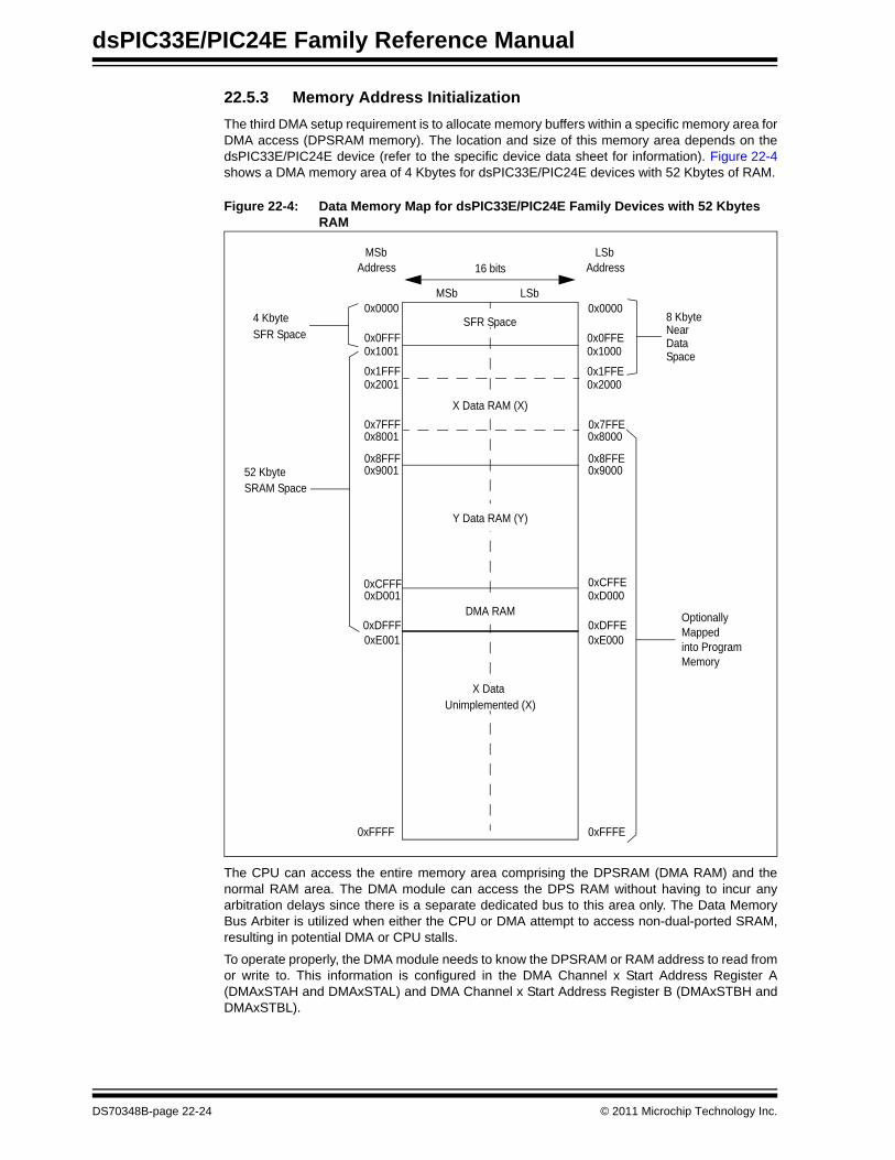
22.5.3 Memory Address InitializationThe third DMA setup requirement is to allocate memory buffers within a specific memory area for DMA access (DPSRAM memory). The location and size of this memory area depends on the dsPIC33E/PIC24E device (refer to the specific device data sheet for information). Figure 22-4 shows a DMA memory area of 4 Kbytes for dsPIC33E/PIC24E devices with 52 Kbytes of RAM.
Figure 22-4: Data Memory Map for dsPIC33E/PIC24E Family Devices with 52 Kbytes RAM
The CPU can access the entire memory area comprising the DPSRAM (DMA RAM) and the normal RAM area. The DMA module can access the DPS RAM without having to incur any arbitration delays since there is a separate dedicated bus to this area only. The Data Memory Bus Arbiter is utilized when either the CPU or DMA attempt to access non-dual-ported SRAM, resulting in potential DMA or CPU stalls.
To operate properly, the DMA module needs to know the DPSRAM or RAM address to read from or write to. This information is configured in the DMA Channel x Start Address Register A (DMAxSTAH and DMAxSTAL) and DMA Channel x Start Address Register B (DMAxSTBH and DMAxSTBL).
0x0000
0x0FFESFR Space
0xFFFE
16 bits
LSbMSb
0xFFFF
X Data
OptionallyMappedinto ProgramMemory
Unimplemented (X)
0x1000
4 KbyteSFR Space
0x90000x8FFE
0xDFFE0xE000
52 KbyteSRAM Space
NearData
8 Kbyte
Space
0xCFFE0xD000
LSbAddress
MSbAddress
0x0000
0x0FFF0x1001
0x90010x8FFF
0xDFFF0xE001
0xCFFF0xD001
0x8001 0x8000
0x1FFE0x2000
0x1FFF0x2001
0x7FFE0x7FFF
DMA RAM
Y Data RAM (Y)
X Data RAM (X)
DS70348B-page 22-24 © 2011 Microchip Technology Inc.
Section 22. Direct Memory Access (DMA)D
irect Mem
ory A
ccess (DM
A)
22
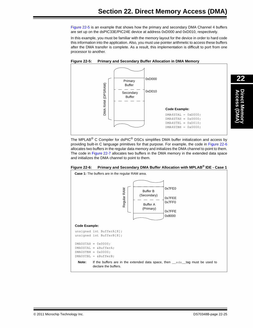
Figure 22-5 is an example that shows how the primary and secondary DMA Channel 4 buffers are set up on the dsPIC33E/PIC24E device at address 0xD000 and 0xD010, respectively.
In this example, you must be familiar with the memory layout for the device in order to hard code this information into the application. Also, you must use pointer arithmetic to access these buffers after the DMA transfer is complete. As a result, this implementation is difficult to port from one processor to another.
Figure 22-5: Primary and Secondary Buffer Allocation in DMA Memory
The MPLAB® C Compiler for dsPIC® DSCs simplifies DMA buffer initialization and access by providing built-in C language primitives for that purpose. For example, the code in Figure 22-6 allocates two buffers in the regular data memory and initializes the DMA channel to point to them. The code in Figure 22-7 allocates two buffers in the DMA memory in the extended data space and initializes the DMA channel to point to them.
Figure 22-6: Primary and Secondary DMA Buffer Allocation with MPLAB® IDE - Case 1
PrimaryBuffer
SecondaryBuffer
0xD000
0xD010
DM
A R
AM
(DP
SR
AM
)Code Example:DMA4STAL = 0xD000;DMA4STAH = 0x0000;DMA4STBL = 0xD010;DMA4STBH = 0x0000;
Buffer B(Secondary)
Buffer A(Primary)
0x7FE0
0x8000
Reg
ular
RA
M
0x7FEE0x7FF0
0x7FFE
Code Example:unsigned int BufferA[8];unsigned int BufferB[8];
DMA0STAH = 0x0000;DMA0STAL = &BufferA;DMA0STBH = 0x0000;DMA0STBL = &BufferB;
Case 1: The buffers are in the regular RAM area.
Note: If the buffers are in the extended data space, then __eds__tag must be used to declare the buffers.
© 2011 Microchip Technology Inc. DS70348B-page 22-25

dsPIC33E/PIC24E Family Reference Manual
Figure 22-7: Primary and Secondary DMA Buffer Allocation with MPLAB® IDE - Case 2
If the DMAxSTA (and/or DMAxSTB) register is initialized to a value that will result in the DMA channel reading or writing RAM addresses outside of accessible space, DMA channel writes to this memory address are ignored. DMA channel reads from this memory address result in a read of ‘0’. If the DMA module attempts to access any unimplemented memory address, a DMA Address Error Trap is issued, and the DMA Address Error Soft Trap Status bit (DAE) is set.
22.5.4 DMA Transfer Count SetupIn the fourth step of the DMA setup process, each DMA channel must be programmed to service N + 1 number of requests before the data block transfer is considered complete. The value ‘N’ is specified by programming the DMA Channel x Transfer Count register (DMAxCNT). That is, a DMAxCNT value of ‘0’ will transfer one element.
The value of the DMAxCNT register is independent of the transfer data size (byte or word), which is specified in the SIZE bit in the DMAxCON register.
If the DMAxCNT register is initialized to a value that will result in the DMA channel reading or writing RAM addresses outside of accessible space, DMA channel writes to this memory address are ignored. DMA channel reads from this memory address result in a read of ‘0’.
22.5.5 Operating Mode SetupThe fifth and final step in DMA setup is to specify the mode of operation for each DMA channel by configuring the DMA Channel x Control register (DMAxCON). See 22.6 “DMA Operating Modes” for specific setup information.
PrimaryBuffer
SecondaryBuffer
0xD000
0xD010
DM
A R
AM
(DP
SR
AM
)Code Example:__eds__ unsigned int BufferA[8] __attribute__((eds,space(dma)));
__eds__ unsigned int BufferB[8] __attribute__((eds,space(dma)));
DMA0STAH = 0x0000;DMA0STAL = __builtin_dmaoffset(BufferA);DMA0STBH = 0x0000;DMA0STBL = __builtin_dmaoffset(BufferB);
Case 2: The buffers are in DMA RAM, in the extended data space.
Note: If the DMA RAM is not a part of the extended data space, then __eds__tag and the eds attribute are not required to declared the buffers.
DS70348B-page 22-26 © 2011 Microchip Technology Inc.

Section 22. Direct Memory Access (DMA)D
irect Mem
ory A
ccess (DM
A)
22
22.6 DMA OPERATING MODESDMA channel supports these modes of operation:
• Word or byte data transfer• Transfer direction (peripheral to memory, or memory to peripheral)• Full or half transfer interrupts to CPU• Post-Increment or static memory addressing• Peripheral Indirect Addressing• One-Shot or continuous block transfers• Auto-switch between two start addresses offsets (DMAxSTA or DMAxSTB) after each
transfer complete (Ping-Pong mode)• Null Data Write mode
Additionally, DMA supports a manual mode, which forces a single DMA transfer.
22.6.1 Word or Byte Data TransferEach DMA channel can be configured to transfer data by word or byte. Word data can only be moved to and from aligned (even) addresses. But, byte data can be moved to or from any (legal) address.
If the SIZE bit (DMAxCON<14>) is clear, word-sized data is transferred. If Register Indirect with Post-Increment Addressing mode is enabled, the address is post-incremented by 2 after every word transfer (see 22.6.5 “Register Indirect without Post-increment Addressing Mode”).
If the SIZE bit is set, byte-sized data is transferred. If Register Indirect with Post-Increment Addressing mode is enabled, the address is incremented by 1 after every byte transfer.
22.6.2 Transfer DirectionEach DMA channel can be configured to transfer data from a peripheral to the DPSRAM/RAM or from the DPSRAM/RAM to a peripheral.
If the Transfer Direction bit (DIR) in the DMAxCON register is clear, data is read from the peripheral (using the Peripheral Address as provided by DMAxPAD) and the destination write is directed to the DPSRAM/RAM memory address (using DMAxSTA or DMAxSTB).
If the DIR bit is set, data is read from the DPSRAM/RAM memory address (using DMAxSTA or DMAxSTB) and the destination write is directed to the peripheral (using the peripheral address, as provided by DMAxPAD).
Once configured, each channel is a unidirectional data conduit. That is, should a peripheral require read and write data using the DMA module, two channels must be assigned – one for read and one for write.
22.6.3 Full or Half-Block Transfer InterruptsEach DMA channel provides an interrupt to the interrupt controller when block data transfer is complete or half complete. This mode is designated by clearing or setting the HALF bit in the DMA Channel x Control register (DMAxCON):
HALF = 0 (initiate interrupt when all of the data has been moved)
HALF = 1 (initiate interrupt when half of the data has been moved)
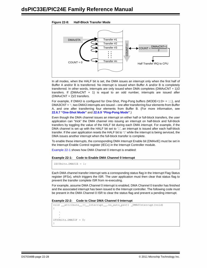
When DMA Continuous mode is used, the CPU must be able to process the incoming or outgoing data at least as fast as the DMA is moving it. The half transfer interrupt helps mitigate this problem by generating an interrupt when only half of the data has been transferred. For example, if an ADC is being continuously read by the DMA controller, the half transfer interrupt allows the CPU to process the buffer before it becomes completely full. Provided it never gets ahead of the DMA writes, this scheme can be used to relax the CPU response time requirements. Figure 22-8 illustrates this process.
© 2011 Microchip Technology Inc. DS70348B-page 22-27
dsPIC33E/PIC24E Family Reference Manual
Figure 22-8: Half-Block Transfer Mode
In all modes, when the HALF bit is set, the DMA issues an interrupt only when the first half of Buffer A and/or B is transferred. No interrupt is issued when Buffer A and/or B is completely transferred. In other words, interrupts are only issued when DMA completes (DMAxCNT + 1)/2 transfers. If (DMAxCNT + 1) is equal to an odd number, interrupts are issued after (DMAxCNT + 2)/2 transfers.
For example, if DMA3 is configured for One-Shot, Ping-Pong buffers (MODE<1:0> = 11), and DMA3CNT = 7, two DMA3 interrupts are issued – one after transferring four elements from Buffer A, and one after transferring four elements from Buffer B. (For more information, see 22.6.7 “One-Shot Mode” and 22.6.9 “Ping-Pong Mode”.)
Even though the DMA channel issues an interrupt on either half or full-block transfers, the user application can “trick” the DMA channel into issuing an interrupt on half-block and full-block transfers by toggling the value of the HALF bit during each DMA interrupt. For example, if the DMA channel is set up with the HALF bit set to ‘1’, an interrupt is issued after each half-block transfer. If the user application resets the HALF bit to ‘0’ while the interrupt is being serviced, the DMA issues another interrupt when the full-block transfer is complete.
To enable these interrupts, the corresponding DMA Interrupt Enable bit (DMAxIE) must be set in the Interrupt Enable Control register (IECx) in the Interrupt Controller module.
Example 22-1 shows how DMA Channel 0 interrupt is enabled:
Example 22-1: Code to Enable DMA Channel 0 Interrupt
Each DMA channel transfer interrupt sets a corresponding status flag in the Interrupt Flag Status register (IFSx), which triggers the ISR. The user application must then clear that status flag to prevent the transfer complete ISR from re-executing.
For example, assume DMA Channel 0 interrupt is enabled, DMA Channel 0 transfer has finished and the associated interrupt has been issued to the Interrupt controller. The following code must be present in the DMA Channel 0 ISR to clear the status flag and prevent a pending interrupt.
Example 22-2: Code to Clear DMA Channel 0 Interrupt
Transfer #1Transfer #2Transfer #3
Transfer #n
CO
UN
T++
COUNT = DMAxCNT+12
DMAxSTA
Half Transfer IRQ to CPUCOUNT = 0
IEC0bits.DMA0IE = 1;
void __attribute__((__interrupt__,no_auto_psv)) _DMA0Interrupt(void){
.
.
.IFS0bits.DMA0IF = 0;}
DS70348B-page 22-28 © 2011 Microchip Technology Inc.

Section 22. Direct Memory Access (DMA)D
irect Mem
ory A
ccess (DM
A)
22
22.6.4 Register Indirect with Post-Increment Addressing ModeRegister Indirect with Post-Increment Addressing mode is used to move blocks of data by incrementing the DPSRAM/RAM address after each transfer.
The DMA channel defaults to this mode after the DMA controller is reset. This mode is selected by programming the Addressing Mode Select bits (AMODE<1:0>) to ‘00’ in the DMA Channel Control register (DMAxCON). In this mode, the Start Address register (DMAxSTA or DMAxSTB) provides the starting address of memory buffer.
The user application determines the latest transfer address by reading the Start Address register. However, the contents of this register are not modified by the DMA controller.
Figure 22-9 illustrates data transfer in this mode.
Figure 22-9: Data Transfer with Register Indirect with Post-Increment Addressing
DMA3STA + 0DMA3STA + 1DMA3STA + 2
Data 1Data 2Data 3
Peripheral 1
DMAChannel 3
DMA Channel 3, First TransferA
DMA3STA + 0DMA3STA + 1DMA3STA + 2
Data 1Data 2Data 3
Peripheral 1
DMAChannel 3
DMA3STA + 0DMA3STA + 1DMA3STA + 2
Data 1Data 2Data 3
Peripheral 1
DMAChannel 3
DMA Channel 3, Second TransferB
DMA Channel 3, Third TransferC
Transfer 1
Transfer 2
Transfer 3
© 2011 Microchip Technology Inc. DS70348B-page 22-29
dsPIC33E/PIC24E Family Reference Manual
Example 22-3: Code for Output Compare and DMA with Register Indirect Post-Increment Mode
Set up Output Compare 1 module for PWM mode:OC1CON1 = 0; // Reset OC moduleOC1CON2 = 0;OC1R = 0x60; // Initialize PWM Duty CycleOC1RS = 0x60; // Initialize PWM Duty Cycle Buffer
OC1CONbits.OCM = 6; // Configure OC for the PWM mode
Set up DMA Channel 3 for Post Increment mode with Timer2 Request source:__eds__ unsigned int BufferA[32] __attribute__((eds));/* Insert code here to initialize BufferA with desired Duty Cycle values */
DMA3CONbits.AMODE = 0; // Configure DMA for Register Indirect mode // with post-increment
DMA3CONbits.MODE = 0; // Configure DMA for Continuous modeDMA3CONbits.DIR = 1; // RAM-to-Peripheral data transfersDMA3PAD = (volatile unsigned int)&OC1RS; // Point DMA to OC1RSDMA3CNT = 31; // 32 DMA requestDMA3REQ = 7; // Select Timer2 as DMA request source
DMA3STAL = __builtin_dmaoffset(BufferA);DMA3STAH = 0x0000;
IFS2bits.DMA3IF = 0; // Clear the DMA Interrupt Flag bitIEC2bits.DMA3IE = 1; // Set the DMA Interrupt Enable bit
DMA3CONbits.CHEN = 1; // Enable DMA
Set up Timer2 for Output Compare PWM mode:PR2 = 0xBF; // Initialize PWM periodT2CONbits.TON = 1; // Start Timer2
Set up DMA Channel 3 Interrupt Handler:void __attribute__((__interrupt__,no_auto_psv)) _DMA3Interrupt(void){
/* Update BufferA with new Duty Cycle values if desired here */
IFS2bits.DMA3IF = 0; //Clear the DMA3 Interrupt Flag}
DS70348B-page 22-30 © 2011 Microchip Technology Inc.
Section 22. Direct Memory Access (DMA)D
irect Mem
ory A
ccess (DM
A)
22
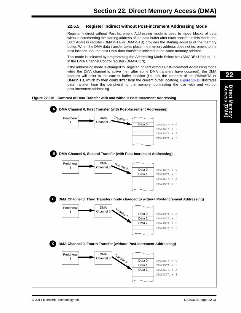
22.6.5 Register Indirect without Post-increment Addressing ModeRegister Indirect without Post-Increment Addressing mode is used to move blocks of data without incrementing the starting address of the data buffer after each transfer. In this mode, the Start Address register (DMAxSTA or DMAxSTB) provides the starting address of the memory buffer. When the DMA data transfer takes place, the memory address does not increment to the next location. So, the next DMA data transfer is initiated to the same memory address.
This mode is selected by programming the Addressing Mode Select bits (AMODE<1:0>) to ‘01’ in the DMA Channel Control register (DMAxCON).
If the addressing mode is changed to Register Indirect without Post-Increment Addressing mode while the DMA channel is active (i.e., after some DMA transfers have occurred), the DMA address will point to the current buffer location (i.e., not the contents of the DMAxSTA or DMAxSTB, which by then could differ from the current buffer location). Figure 22-10 illustrates data transfer from the peripheral to the memory, contrasting the use with and without post-increment addressing.
Figure 22-10: Contrast of Data Transfer with and without Post-Increment Addressing
DMA3STA + 0DMA3STA + 1DMA3STA + 2
Data 0
Peripheral 1
DMAChannel 0
DMA Channel 0, First Transfer (with Post-Increment Addressing)A
DMA3STA + 0DMA3STA + 1DMA3STA + 2
Data 0Data 1Data 2
Peripheral 1
DMAChannel 0
DMA3STA + 0DMA3STA + 1DMA3STA + 2
Data 0Data 1
Peripheral 1
DMAChannel 0
DMA Channel 0, Second Transfer (with Post-Increment Addressing)B
DMA Channel 0, Third Transfer (mode changed to without Post-Increment Addressing)C
DMA3STA + 0DMA3STA + 1DMA3STA + 2
Data 0Data 1Data 3
Peripheral 1
DMAChannel 0
DMA Channel 0, Fourth Transfer (without Post-Increment Addressing)C
DMA3STA + 3
DMA3STA + 3
DMA3STA + 3
DMA3STA + 3
Transfer 1
Transfer 2
Transfer 3
Transfer 4
© 2011 Microchip Technology Inc. DS70348B-page 22-31
dsPIC33E/PIC24E Family Reference Manual
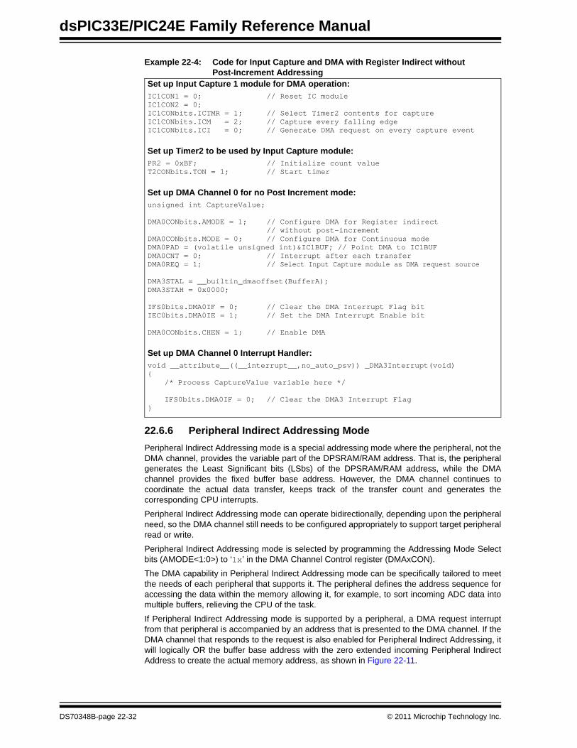
Example 22-4: Code for Input Capture and DMA with Register Indirect without Post-Increment Addressing
22.6.6 Peripheral Indirect Addressing ModePeripheral Indirect Addressing mode is a special addressing mode where the peripheral, not the DMA channel, provides the variable part of the DPSRAM/RAM address. That is, the peripheral generates the Least Significant bits (LSbs) of the DPSRAM/RAM address, while the DMA channel provides the fixed buffer base address. However, the DMA channel continues to coordinate the actual data transfer, keeps track of the transfer count and generates the corresponding CPU interrupts.
Peripheral Indirect Addressing mode can operate bidirectionally, depending upon the peripheral need, so the DMA channel still needs to be configured appropriately to support target peripheral read or write.
Peripheral Indirect Addressing mode is selected by programming the Addressing Mode Select bits (AMODE<1:0>) to ‘1x’ in the DMA Channel Control register (DMAxCON).
The DMA capability in Peripheral Indirect Addressing mode can be specifically tailored to meet the needs of each peripheral that supports it. The peripheral defines the address sequence for accessing the data within the memory allowing it, for example, to sort incoming ADC data into multiple buffers, relieving the CPU of the task.
If Peripheral Indirect Addressing mode is supported by a peripheral, a DMA request interrupt from that peripheral is accompanied by an address that is presented to the DMA channel. If the DMA channel that responds to the request is also enabled for Peripheral Indirect Addressing, it will logically OR the buffer base address with the zero extended incoming Peripheral Indirect Address to create the actual memory address, as shown in Figure 22-11.
Set up Input Capture 1 module for DMA operation:IC1CON1 = 0; // Reset IC moduleIC1CON2 = 0;IC1CONbits.ICTMR = 1; // Select Timer2 contents for captureIC1CONbits.ICM = 2; // Capture every falling edgeIC1CONbits.ICI = 0; // Generate DMA request on every capture event
Set up Timer2 to be used by Input Capture module:PR2 = 0xBF; // Initialize count valueT2CONbits.TON = 1; // Start timer
Set up DMA Channel 0 for no Post Increment mode:unsigned int CaptureValue;
DMA0CONbits.AMODE = 1; // Configure DMA for Register indirect // without post-increment
DMA0CONbits.MODE = 0; // Configure DMA for Continuous modeDMA0PAD = (volatile unsigned int)&IC1BUF; // Point DMA to IC1BUFDMA0CNT = 0; // Interrupt after each transferDMA0REQ = 1; // Select Input Capture module as DMA request source
DMA3STAL = __builtin_dmaoffset(BufferA);DMA3STAH = 0x0000;
IFS0bits.DMA0IF = 0; // Clear the DMA Interrupt Flag bitIEC0bits.DMA0IE = 1; // Set the DMA Interrupt Enable bit
DMA0CONbits.CHEN = 1; // Enable DMA
Set up DMA Channel 0 Interrupt Handler:void __attribute__((__interrupt__,no_auto_psv)) _DMA3Interrupt(void){
/* Process CaptureValue variable here */
IFS0bits.DMA0IF = 0; // Clear the DMA3 Interrupt Flag}
DS70348B-page 22-32 © 2011 Microchip Technology Inc.

Section 22. Direct Memory Access (DMA)D
irect Mem
ory A
ccess (DM
A)
22
Figure 22-11: Address Offset Generation in Peripheral Indirect Addressing Mode
The peripheral determines how many Least Significant address bits it will control. The application program must select a base address for the buffer in memory and ensure that the corresponding number of Least Significant bits of that address offset are zero. As with other modes, when the DMA Start Address register is read, it returns a value of the latest memory transfer address, which includes the address calculation described above. If the DMA channel is not configured for Peripheral Indirect Addressing, the incoming address is ignored and the data transfer occurs as normal.
Peripheral Indirect Addressing mode is compatible with all other operating modes and is currently supported by the ADC and ECAN modules.
22.6.6.1 ADC SUPPORT FOR DMA ADDRESS GENERATION
In Peripheral Indirect Addressing mode, the peripheral defines the addressing sequence, which is more tailored to peripheral functionality. For example, if the ADC is configured to continuously convert inputs 0 through 3 in sequence (for example, 0, 1, 2, 3, 0, 1, and so on) and is associated with a DMA channel that is configured for Register Indirect Addressing with Post-Increment, the DMA transfer moves this data into a sequential buffer as shown in Figure 22-12. Example 22-5 illustrates the code for this configuration.
Figure 22-12: Data Transfer from ADC with Register Indirect Addressing
Address(from DMAxSTA or DMAxSTB)
Peripheral Indirect Address(from peripheral)
PIA Address0. . . .0
0. . . .0 Address
Memory Address
Application Responsibility:Set to ‘0’
Zero Extend
DMA5STA+PIA (for Transfer 1)
ADC DMAChannel
5
AN 0AN 1AN 2AN 3
Data
DMARequest
AN0 Sample 1AN1 Sample 1
AN2 Sample 1
AN0 Sample 2
AN0 Sample 3
AN2 Sample 2AN1 Sample 2
AN1 Sample 3
AN2 Sample 3
AN3 Sample 1
AN3 Sample 2
AN3 Sample 3
Transfer 1Transfer 2
Transfer 12
Transfer 3
© 2011 Microchip Technology Inc. DS70348B-page 22-33

dsPIC33E/PIC24E Family Reference Manual
Example 22-5: Code for Data Transfer from ADC with Register Indirect AddressingSet up ADC1 for Channel 0-3 sampling:AD1CON1bits.FORM = 3; // Data Output Format: Signed Fraction (Q15 format)AD1CON1bits.SSRC = 2; // Sample Clock Source: GP Timer starts conversionAD1CON1bits.ASAM = 1; // Sampling begins immediately after conversionAD1CON1bits.AD12B = 0; // 10-bit ADC operationAD1CON1bits.SIMSAM = 0; // Samples individual channels sequentially
AD1CON2bits.BUFM = 0;AD1CON2bits.CSCNA = 1; // Scan CH0+ Input Selections during Sample A bitAD1CON2bits.CHPS = 0; // Converts CH0
AD1CON3bits.ADRC = 0; // ADC Clock is derived from Systems ClockAD1CON3bits.ADCS = 63; // ADC Conversion Clock
AD1CON4bits.ADDMAEN = 1;//AD1CHS0: Analog-to-Digital Input Select RegisterAD1CHS0bits.CH0SA = 0; // MUXA +ve input selection (AIN0) for CH0AD1CHS0bits.CH0NA = 0; // MUXA -ve input selection (VREF-) for CH0
//AD1CHS123: Analog-to-Digital Input Select RegisterAD1CHS123bits.CH123SA = 0; // MUXA +ve input selection (AIN0) for CH1AD1CHS123bits.CH123NA = 0; // MUXA -ve input selection (VREF-) for CH1
//AD1CSSH/AD1CSSL: Analog-to-Digital Input Scan Selection RegisterAD1CSSH = 0x0000;AD1CSSL = 0x000F; // Scan AIN0, AIN1, AIN2, AIN3 inputs
Set up Timer3 to trigger ADC1 conversions:TMR3 = 0x0000;PR3 = 4999; // Trigger ADC1 every 125 μs @ 40 MIPSIFS0bits.T3IF = 0; // Clear Timer3 interruptIEC0bits.T3IE = 0; // Disable Timer3 interrupt
T3CONbits.TON = 1; // Start Timer3
Set up DMA Channel 5 for Register Indirect with Post-Increment Addressing:__eds__ unsigned int BufferA[32] __attribute__((eds,space(dma)));__eds__ unsigned int BufferB[32] __attribute__((eds,space(dma)));
DMA5CONbits.AMODE = 0; // Configure DMA for Register Indirect mode // with post-increment
DMA5CONbits.MODE = 2; // Configure DMA for Continuous Ping-Pong modeDMA5PAD = (volatile unsigned int)&ADC1BUF0; // Point DMA to ADC1BUF0DMA5CNT = 31; // 32 DMA requestDMA5REQ = 13; // Select ADC1 as DMA Request source
DMA5STAL = __builtin_dmaoffset(BufferA);DMA5STAH = 0x0000;
DMA5STBL = __builtin_dmaoffset(BufferB);DMA5STBH = 0x0000;
IFS3bits.DMA5IF = 0; // Clear the DMA Interrupt Flag bitIEC3bits.DMA5IE = 1; // Set the DMA Interrupt Enable bit
DMA5CONbits.CHEN = 1; // Enable DMA
DS70348B-page 22-34 © 2011 Microchip Technology Inc.
Section 22. Direct Memory Access (DMA)D
irect Mem
ory A
ccess (DM
A)
22
Example 22-5: Code for Data Transfer from ADC with Register Indirect Addressing (Continued)
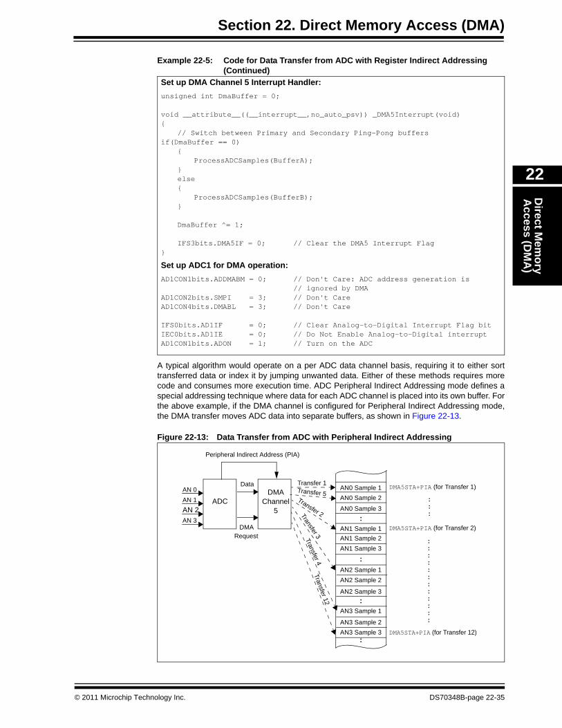
A typical algorithm would operate on a per ADC data channel basis, requiring it to either sort transferred data or index it by jumping unwanted data. Either of these methods requires more code and consumes more execution time. ADC Peripheral Indirect Addressing mode defines a special addressing technique where data for each ADC channel is placed into its own buffer. For the above example, if the DMA channel is configured for Peripheral Indirect Addressing mode, the DMA transfer moves ADC data into separate buffers, as shown in Figure 22-13.
Figure 22-13: Data Transfer from ADC with Peripheral Indirect Addressing
Set up DMA Channel 5 Interrupt Handler:unsigned int DmaBuffer = 0;
void __attribute__((__interrupt__,no_auto_psv)) _DMA5Interrupt(void){
// Switch between Primary and Secondary Ping-Pong buffersif(DmaBuffer == 0)
{ProcessADCSamples(BufferA);
}else{
ProcessADCSamples(BufferB);}
DmaBuffer ^= 1;
IFS3bits.DMA5IF = 0; // Clear the DMA5 Interrupt Flag}
Set up ADC1 for DMA operation:AD1CON1bits.ADDMABM = 0; // Don't Care: ADC address generation is
// ignored by DMAAD1CON2bits.SMPI = 3; // Don't CareAD1CON4bits.DMABL = 3; // Don't Care IFS0bits.AD1IF = 0; // Clear Analog-to-Digital Interrupt Flag bitIEC0bits.AD1IE = 0; // Do Not Enable Analog-to-Digital interrupt AD1CON1bits.ADON = 1; // Turn on the ADC
DMA5STA+PIA (for Transfer 1)
ADCDMA
Channel5
AN 0AN 1AN 2AN 3
Data
DMARequest
AN0 Sample 1AN0 Sample 2
AN0 Sample 3
AN1 Sample 1
AN2 Sample 1
AN1 Sample 3AN1 Sample 2
AN2 Sample 2
AN2 Sample 3
AN3 Sample 1
AN3 Sample 2AN3 Sample 3
:
:
:
:
DMA5STA+PIA (for Transfer 2)
DMA5STA+PIA (for Transfer 12)
:::
::::::::::::
Transfer 1Transfer 5Transfer 2Transfer 3Transfer 4
Transfer 12
Peripheral Indirect Address (PIA)
© 2011 Microchip Technology Inc. DS70348B-page 22-35

dsPIC33E/PIC24E Family Reference Manual
To enable this kind of ADC addressing, the DMA Buffer Build Mode bit (ADDMABM) in the ADCx Control 1 register (ADxCON1) must be cleared. If this bit is set, the ADC generates addresses in the order of conversion (same as DMA Register Indirect Addressing with Post-Increment mode).
As mentioned earlier, the user must pay special attention to the number of Least Significant bits that are reserved for the peripheral when the DMA Start Address registers (DMAxSTA and DMAxSTB) are initialized by the user application. For the ADC, the number of bits depends on the size and number of the ADC buffers.
The number of ADC buffers is initialized with the Increment Rate for DMA Addresses bits (SMPI<4:0>) in the ADCx Control 2 register (ADxCON2). The size of each ADC buffer is initialized with the Number of DMA Buffer Locations per Analog Input bits (DMABL<2:0>) in the ADCx Control 4 register (ADCxCON4). For example, if SMPI<4:0> bits are initialized to 3 and DMABL<2:0> bits are initialized to 3, there will be four ADC buffers (SMPI<4:0> + 1), each with eight words (2 DMABL<2:0>), for a total of 32 words (64 bytes). This means that the address that is written into the DMAxSTA and DMAxSTB must have 6 (26 bits = 64 bytes) Least Significant bits set to zero.
If the MPLAB C Compiler for dsPIC DSCs is used to initialize the DMAxSTA and DMAxSTB registers, proper data alignment must be specified via data attributes. For the above conditions, the code shown in Example 22-6 will properly initialize DMAxSTA and DMAxSTB registers.
Example 22-6: DMA Buffer Alignment with MPLAB® C Compiler for dsPIC® DSCs
Example 22-7 illustrates the code for this configuration.
Example 22-7: Code for ADC and DMA with Peripheral Indirect Addressing
__eds__ intBufferA[4][8] __attribute__((eds,aligned(64)));__eds__ intBufferB[4][8] __attribute__((eds,aligned(64)));
DMA0STAL = __builtin_dmaoffset(BufferA);DMA0STAH = 0x0000;
DMA0STBL = __builtin_dmaoffset(BufferB);DMA0STBH = 0x0000;
Set up ADC1 for Channel 0-3 sampling:AD1CON1bits.FORM = 3; // Data Output Format: Signed Fraction (Q15 format)AD1CON1bits.SSRC = 2; // Sample Clock Source: GP timer starts conversionAD1CON1bits.ASAM = 1; // Sampling begins immediately after conversionAD1CON1bits.AD12B = 0; // 10-bit ADC operationAD1CON1bits.SIMSAM = 0; // Samples multiple channels sequentially
AD1CON2bits.BUFM = 0;AD1CON2bits.CSCNA = 1; // Scan CH0+ Input Selections during Sample A bitAD1CON2bits.CHPS = 0; // Converts CH0
AD1CON3bits.ADRC = 0; // ADC clock is derived from systems clockAD1CON3bits.ADCS = 63; // ADC conversion clock
AD1CON4bits.ADDMAEN = 1;//AD1CHS0: Analog-to-Digital Input Select RegisterAD1CHS0bits.CH0SA = 0; // MUXA +ve input selection (AIN0) for CH0AD1CHS0bits.CH0NA = 0; // MUXA -ve input selection (VREF-) for CH0
//AD1CHS123: Analog-to-Digital Input Select RegisterAD1CHS123bits.CH123SA = 0;// MUXA +ve input selection (AIN0) for CH1AD1CHS123bits.CH123NA = 0;// MUXA -ve input selection (VREF-) for CH1
//AD1CSSH/AD1CSSL: Analog-to-Digital Input Scan Selection RegisterAD1CSSH = 0x0000;AD1CSSL = 0x000F; // Scan AIN0, AIN1, AIN2, AIN3 inputs
Set up Timer3 to trigger ADC1 conversions:TMR3 = 0x0000;PR3 = 4999;// Trigger ADC1 every 125usecIFS0bits.T3IF = 0; // Clear Timer3 interruptIEC0bits.T3IE = 0; // Disable Timer3 interrupt
T3CONbits.TON = 1; // Start Timer3
DS70348B-page 22-36 © 2011 Microchip Technology Inc.

Section 22. Direct Memory Access (DMA)D
irect Mem
ory A
ccess (DM
A)
22
Example 22-7: Code for ADC and DMA with Peripheral Indirect Addressing (Continued)Set up DMA Channel 5 for Peripheral Indirect Addressing:struct{
unsigned int Adc1Ch0[8];unsigned int Adc1Ch1[8];unsigned int Adc1Ch2[8];unsigned int Adc1Ch3[8];
} BufferA;
struct{
unsigned int Adc1Ch0[8];unsigned int Adc1Ch1[8];unsigned int Adc1Ch2[8];unsigned int Adc1Ch3[8];
} BufferB;
DMA5CONbits.AMODE = 2; // Configure DMA for Peripheral Indirect modeDMA5CONbits.MODE = 2; // Configure DMA for Continuous Ping-Pong modeDMA5PAD = (volatile unsigned int)&ADC1BUF0; // Point DMA to ADC1BUF0DMA5CNT = 31; // 32 DMA request (4 buffers, each with 8 words)DMA5REQ = 13; // Select ADC1 as DMA request source
DMA5STAL = &BufferA;DMA5STAH = 0x0000;
DMA5STBL = &BufferB;DMA5STBH = 0x0000;
IFS3bits.DMA5IF = 0; // Clear the DMA Interrupt Flag bitIEC3bits.DMA5IE = 1; // Set the DMA Interrupt Enable bitDMA5CONbits.CHEN=1; // Enable DMA
Set up DMA Channel 5 Interrupt Handler:unsigned int DmaBuffer = 0;
void __attribute__((__interrupt__,no_auto_psv)) _DMA5Interrupt(void){
// Switch between Primary and Secondary Ping-Pong buffersif(DmaBuffer == 0)
{ProcessADCSamples(BufferA.Adc1Ch0);ProcessADCSamples(BufferA.Adc1Ch1);ProcessADCSamples(BufferA.Adc1Ch2);ProcessADCSamples(BufferA.Adc1Ch3);
}else{
ProcessADCSamples(BufferB.Adc1Ch0);ProcessADCSamples(BufferB.Adc1Ch1);ProcessADCSamples(BufferB.Adc1Ch2);ProcessADCSamples(BufferB.Adc1Ch3);
}
DmaBuffer ^= 1;
IFS3bits.DMA5IF = 0; // Clear the DMA5 Interrupt Flag}
Set up ADC1 for DMA operation:AD1CON1bits.ADDMABM = 0; // DMA buffers are built in scatter/gather modeAD1CON2bits.SMPI = 3; // 4 ADC buffersAD1CON4bits.DMABL = 3; // Each buffer contains 8 words IFS0bits.AD1IF = 0; // Clear Analog-to-Digital Interrupt Flag bitIEC0bits.AD1IE = 0; // Do Not Enable Analog-to-Digital interrupt AD1CON1bits.ADON = 1; // Turn on the ADC
© 2011 Microchip Technology Inc. DS70348B-page 22-37
dsPIC33E/PIC24E Family Reference Manual
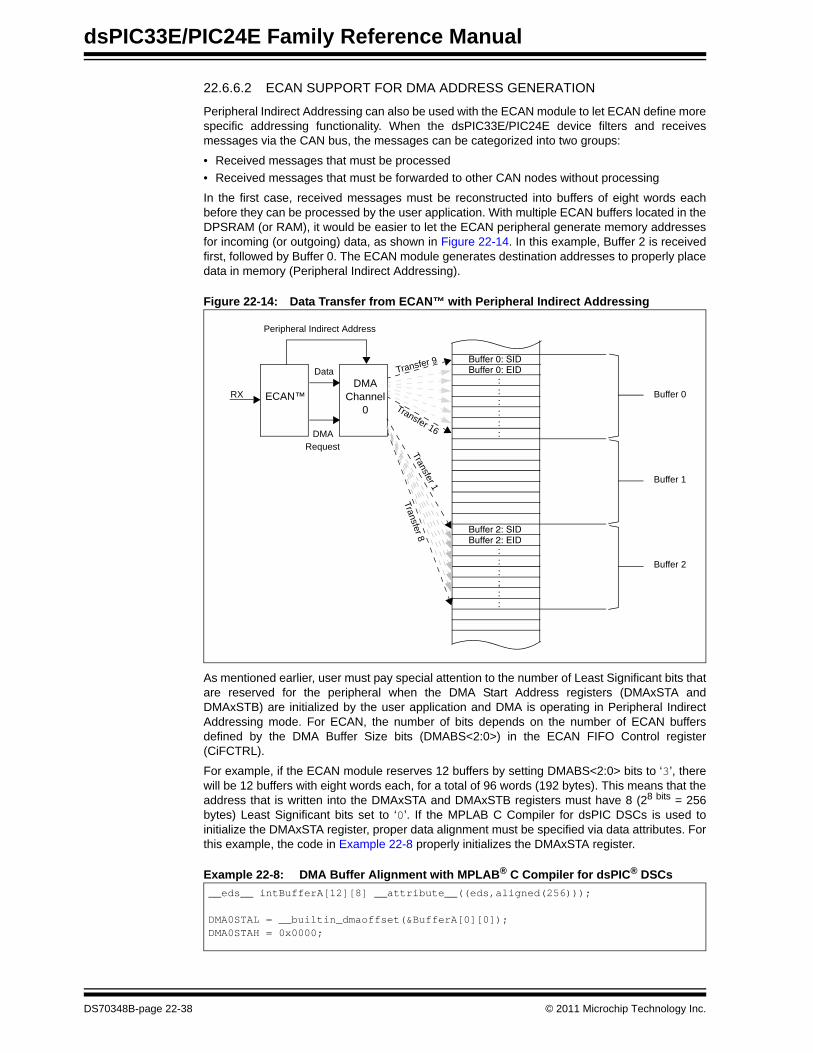
22.6.6.2 ECAN SUPPORT FOR DMA ADDRESS GENERATION
Peripheral Indirect Addressing can also be used with the ECAN module to let ECAN define more specific addressing functionality. When the dsPIC33E/PIC24E device filters and receives messages via the CAN bus, the messages can be categorized into two groups:
• Received messages that must be processed• Received messages that must be forwarded to other CAN nodes without processing
In the first case, received messages must be reconstructed into buffers of eight words each before they can be processed by the user application. With multiple ECAN buffers located in the DPSRAM (or RAM), it would be easier to let the ECAN peripheral generate memory addresses for incoming (or outgoing) data, as shown in Figure 22-14. In this example, Buffer 2 is received first, followed by Buffer 0. The ECAN module generates destination addresses to properly place data in memory (Peripheral Indirect Addressing).
Figure 22-14: Data Transfer from ECAN™ with Peripheral Indirect Addressing
As mentioned earlier, user must pay special attention to the number of Least Significant bits that are reserved for the peripheral when the DMA Start Address registers (DMAxSTA and DMAxSTB) are initialized by the user application and DMA is operating in Peripheral Indirect Addressing mode. For ECAN, the number of bits depends on the number of ECAN buffers defined by the DMA Buffer Size bits (DMABS<2:0>) in the ECAN FIFO Control register (CiFCTRL).
For example, if the ECAN module reserves 12 buffers by setting DMABS<2:0> bits to ‘3’, there will be 12 buffers with eight words each, for a total of 96 words (192 bytes). This means that the address that is written into the DMAxSTA and DMAxSTB registers must have 8 (28 bits = 256 bytes) Least Significant bits set to ‘0’. If the MPLAB C Compiler for dsPIC DSCs is used to initialize the DMAxSTA register, proper data alignment must be specified via data attributes. For this example, the code in Example 22-8 properly initializes the DMAxSTA register.
Example 22-8: DMA Buffer Alignment with MPLAB® C Compiler for dsPIC® DSCs
Buffer 0: SIDBuffer 0: EID
::::::
Buffer 2: SIDBuffer 2: EID
:::;::
ECAN™DMA
Channel0
RX
Data
DMARequest
Transfer 9
Transfer 1
Transfer 8
Peripheral Indirect Address
Transfer 16
Buffer 0
Buffer 1
Buffer 2
__eds__ intBufferA[12][8] __attribute__((eds,aligned(256)));
DMA0STAL = __builtin_dmaoffset(&BufferA[0][0]);DMA0STAH = 0x0000;
DS70348B-page 22-38 © 2011 Microchip Technology Inc.
Section 22. Direct Memory Access (DMA)D
irect Mem
ory A
ccess (DM
A)
22
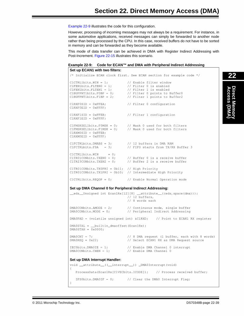
Example 22-9 illustrates the code for this configuration.
However, processing of incoming messages may not always be a requirement. For instance, in some automotive applications, received messages can simply be forwarded to another node rather than being processed by the CPU. In this case, received buffers do not have to be sorted in memory and can be forwarded as they become available.
This mode of data transfer can be achieved in DMA with Register Indirect Addressing with Post-Increment. Figure 22-15 illustrates this scenario.
Example 22-9: Code for ECAN™ and DMA with Peripheral Indirect AddressingSet up ECAN1 with two filters:/* Initialize ECAN clock first. See ECAN section for example code */
C1CTRL1bits.WIN = 1; // Enable filter windowC1FEN1bits.FLTEN0 = 1; // Filter 0 is enabledC1FEN1bits.FLTEN1 = 1; // Filter 1 is enabledC1BUFPNT1bits.F0BP = 0; // Filter 0 points to Buffer0C1BUFPNT1bits.F1BP = 2; // Filter 1 points to Buffer2
C1RXF0SID = 0xFFEA; // Filter 0 configurationC1RXF0EID = 0xFFFF;
C1RXF1SID = 0xFFEB; // Filter 1 configurationC1RXF1EID = 0xFFFF;
C1FMSKSEL1bits.F0MSK = 0; // Mask 0 used for both filtersC1FMSKSEL1bits.F1MSK = 0; // Mask 0 used for both filtersC1RXM0SID = 0xFFEB;C1RXM0EID = 0xFFFF;
C1FCTRLbits.DMABS = 3; // 12 buffers in DMA RAMC1FCTRLbits.FSA = 3; // FIFO starts from TX/RX Buffer 3
C1CTRL1bits.WIN = 0;C1TR01CONbits.TXEN0 = 0; // Buffer 0 is a receive bufferC1TR23CONbits.TXEN2 = 0; // Buffer 2 is a receive buffer
C1TR01CONbits.TX0PRI = 0b11; // High PriorityC1TR01CONbits.TX1PRI = 0b10; // Intermediate High Priority
C1CTRL1bits.REQOP = 0; // Enable Normal Operation mode
Set up DMA Channel 0 for Peripheral Indirect Addressing:__eds__Unsigned int Ecan1Rx[12][8] __attribute__((eds,space(dma)));
// 12 buffers, // 8 words each
DMA0CONbits.AMODE = 2; // Continuous mode, single bufferDMA0CONbits.MODE = 0; // Peripheral Indirect Addressing
DMA0PAD = (volatile unsigned int) &C1RXD; // Point to ECAN1 RX register
DMA0STAL = __builtin_dmaoffset(Ecan1Rx);DMA0STAH = 0x0000;
DMA0CNT = 7; // 8 DMA request (1 buffer, each with 8 words)DMA0REQ = 0x22; // Select ECAN1 RX as DMA Request source
IEC0bits.DMA0IE = 1; // Enable DMA Channel 0 interruptDMA0CONbits.CHEN = 1; // Enable DMA Channel 0
Set up DMA Interrupt Handler:void __attribute__((__interrupt__)) _DMA0Interrupt(void){ ProcessData(Ecan1Rx[C1VECbits.ICODE]); // Process received buffer; IFS0bits.DMA0IF = 0; // Clear the DMA0 Interrupt Flag;}
© 2011 Microchip Technology Inc. DS70348B-page 22-39

dsPIC33E/PIC24E Family Reference Manual
Figure 22-15: Data Transfer from ECAN™ with Register Indirect Addressing
ECAN 1
Buffer 2: SIDBuffer 2: EID
::::::
ECAN™ 1
DMAChannel
0
RX
Data
DMARequest
Transfer 1
Transfer 8
Buffer 2
Buffer 2: SIDBuffer 2: EID
::::::
Buffer 0: SIDBuffer 0: EID
::::::
ECAN 1
DMAChannel
0
RX
Data
DMARequest
Transfer 9
Transfer 16 Buffer 0
Buffer 2: SIDBuffer 2: EID
::::::
Buffer 0: SIDBuffer 0: EID
::::::
Transfer 9
Transfer 1
6
DMAChannel
1ECAN
1
TXData
DMARequest
Transfer 1
Transfer 8
DMAChannel
1
TXData
DMARequest
Receive Buffer 2A
Receive Buffer 0 and Transmit Buffer 2B
Transmit Buffer 0C
DS70348B-page 22-40 © 2011 Microchip Technology Inc.

Section 22. Direct Memory Access (DMA)D
irect Mem
ory A
ccess (DM
A)
22
22.6.7 One-Shot ModeOne-Shot mode is used by the application program when repetitive data transfer is not required. This mode is selected by programming the Operating Mode Select bits (MODE<1:0>) to ‘x1’ in the DMA Channel Control register (DMAxCON). In this mode, when the entire data block is moved (block length as defined by DMAxCNT), the data block end is detected and the channel is automatically disabled (i.e., the CHEN bit in the DMA Channel Control register (DMAxCON) is cleared by the hardware). Figure 22-16 illustrates One-Shot mode.
Figure 22-16: Data Block Transfer in One-Shot Mode
If the HALF bit in the DMA Channel Control register (DMAxCON) is set, the DMAxIF bit is set (and the DMA interrupt is generated, if enabled by the application program) when half of the data block transfer is complete and the channel remains enabled. When the full-block transfer is complete, no interrupt flag is set and the channel is automatically disabled. For information on setting up the DMA channel to interrupt on both half and full-block transfer, see 22.6.3 “Full or Half-Block Transfer Interrupts”.
If the channel is re-enabled by setting the CHEN bit in the DMAxCON register to ‘1’, the block transfer takes place from the start address, as provided by the DMA Start Address registers (DMAxSTA and DMAxSTB). Example 22-10 illustrates the code for One-Shot operation.
Example 22-10: Code for UART and DMA with One-Shot Mode
TRANSFER #1TRANSFER #2
TRANSFER #3
TRANSFER #n
CO
UN
T++
COUNT =DMAxCNT+1
DMAxSTA
CPUBlock Transfer
CompleteIRQ
Set up UART for RX and TX:#define FCY 40000000#define BAUDRATE 9600 #define BRGVAL ((FCY/BAUDRATE)/16) - 1
U2MODEbits.STSEL = 0; // 1-stop bitU2MODEbits.PDSEL = 0; // No parity, 8-data bitsU2MODEbits.ABAUD = 0; // Auto-baud disabled
U2BRG = BRGVAL; // Baud rate setting for 9600
U2STAbits.UTXISEL0 = 0; // Interrupt after one TX character is transmittedU2STAbits.UTXISEL1 = 0; U2STAbits.URXISEL = 0; // Interrupt after one RX character is received
U2MODEbits.UARTEN = 1; // Enable UARTU2STAbits.UTXEN = 1; // Enable UART TX
© 2011 Microchip Technology Inc. DS70348B-page 22-41

dsPIC33E/PIC24E Family Reference Manual
Example 22-10: Code for UART and DMA with One-Shot Mode (Continued)Set up DMA Channel 0 to Transmit in One-Shot, Single-Buffer mode:unsigned int BufferA[8];unsigned int BufferB[8];
DMA0CON = 0x2001; // One-Shot, Post-Increment, RAM-to-PeripheralDMA0CNT = 7; // Eight DMA requestsDMA0REQ = 0x001F; // Select UART2 transmitter
DMA0PAD = (volatile unsigned int) &U2TXREG;
DMA0STAL = __builtin_dmaoffset(BufferA);DMA0STAH = 0x0000;
IFS0bits.DMA0IF = 0; // Clear DMA Interrupt FlagIEC0bits.DMA0IE = 1; // Enable DMA interrupt
Set up DMA Channel 1 to Receive in Continuous Ping-Pong mode:DMA1CON = 0x0002; // Continuous, Ping-Pong, Post-Inc., Periph-RAMDMA1CNT = 7; // Eight DMA requestsDMA1REQ = 0x001E; // Select UART2 receiver
DMA1PAD = (volatile unsigned int) &U2RXREG;
DMA1STAL = &BufferA;DMA1STAH = 0x0000;
DMA1STBL = &BufferB;DMA1STBH = 0x0000;
IFS0bits.DMA1IF = 0; // Clear DMA interruptIEC0bits.DMA1IE = 1; // Enable DMA interruptDMA1CONbits.CHEN = 1; // Enable DMA channel
Set up DMA Interrupt Handler:void __attribute__((__interrupt__,no_auto_psv)) _DMA0Interrupt(void){ IFS0bits.DMA0IF = 0; // Clear the DMA0 Interrupt Flag}
void __attribute__((__interrupt__,no_auto_psv)) _DMA1Interrupt(void){ static unsigned int BufferCount = 0; // Keep record of which buffer
// contains RX Data
if(BufferCount == 0) {
DMA0STAL = __builtin_dmaoffset(BufferA);DMA0STAH = 0x0000;}else
{DMA0STBL = __builtin_dmaoffset(BufferB);DMA0STBH = 0x0000;}DMA0CONbits.CHEN = 1; // Enable DMA0 channelDMA0REQbits.FORCE = 1; // Manual mode: Kick-start the 1st transfer
BufferCount ^= 1;IFS0bits.DMA1IF = 0; // Clear the DMA1 Interrupt Flag
}
DS70348B-page 22-42 © 2011 Microchip Technology Inc.

Section 22. Direct Memory Access (DMA)D
irect Mem
ory A
ccess (DM
A)
22
22.6.8 Continuous ModeContinuous mode is used by the application program when repetitive data transfer is required throughout the life of the program.
This mode is selected by programming the Operating Mode Select bits (MODE<1:0>) to ‘x0’ in the DMA Channel Control register (DMAxCON). In this mode, when the entire data block is moved (block length as defined by DMAxCNT), the data block end is detected and the channel remains enabled. During the last data transfer, the DMA DPSRAM/RAM address resets back to the (primary) DMA Start Address A register (DMAxSTA). Figure 22-17 illustrates Continuous mode.
Figure 22-17: Repetitive Data Block Transfer with Continuous Mode
If the HALF bit is set in the DMA Channel Control register (DMAxCON), the DMAxIF bit is set (and the DMA interrupt is generated, if enabled) when half of the data block transfer is complete. The channel remains enabled. When the full-block transfer is complete, no interrupt flag is set and the channel remains enabled. For information on how to set up the DMA channel to interrupt on both half and full-block transfer, see 22.6.3 “Full or Half-Block Transfer Interrupts”.
22.6.9 Ping-Pong ModePing-Pong mode allows the CPU to process one buffer while a second buffer operates with the DMA channel. The net result is that the CPU has the entire DMA block transfer time in which to process the buffer currently not being used by the DMA channel. Of course, this transfer mode doubles the amount of memory needed for a given buffer size.
In all DMA operating modes, when the DMA channel is enabled, the (primary) DMA Channel x Memory Start Address A register (DMAxSTA) is selected by default to generate the initial memory effective address. As each block transfer completes and the DMA channel is reinitialized, the buffer start address is sourced from the same DMAxSTA register.
In Ping-Pong mode, the buffer start address is derived from two registers:
• Primary: DMA Channel x Start Address A register (DMAxSTA)• Secondary: DMA Channel x Start Address B register (DMAxSTB)
DMA uses a secondary buffer for alternate block transfers. As each block transfer completes and the DMA channel is reinitialized, the buffer start address is derived from the alternate register.
Ping-Pong mode is selected by programming the Operating Mode Select bits (MODE<1:0>) to ‘1x’ in the DMA Channel Control register (DMAxCON).
Transfer #1Transfer #2Transfer #3
Transfer #n
COUNT++DMAxSTA
COUNT = 0 Count = DMAxCNT + 1
CPUBlock Transfer
CompleteIRQ
© 2011 Microchip Technology Inc. DS70348B-page 22-43

dsPIC33E/PIC24E Family Reference Manual
If Continuous mode is selected while DMA is operating in Ping-Pong mode, DMA responds by reinitializing to point to the secondary buffer after transferring the primary buffer, after which it transfers the secondary buffer. Subsequent block transfers alternate between primary and secondary buffers. Interrupts are generated (if enabled by the application program) after each buffer is transferred. Figure 22-18 illustrates Ping-Pong mode with Continuous operation. Example 22-11 illustrates the code used for Ping-Pong operation using the DCI module as an example.
Figure 22-18: Repetitive Data Transfer in Ping-Pong Mode
Transfer #1Transfer #2Transfer #3
Transfer #n
CO
UN
T++
DMAxSTA
COUNT = 0
COUNT = DMAxCNT+1
CPU Block TransferComplete IRQTransfer #1
Transfer #2Transfer #3
Transfer #nC
OU
NT+
+
DMAxSTB
COUNT = DMAxCNT+1
CPU Block TransferComplete IRQ
Buffer A (Primary)
Buffer B (Secondary)
DS70348B-page 22-44 © 2011 Microchip Technology Inc.
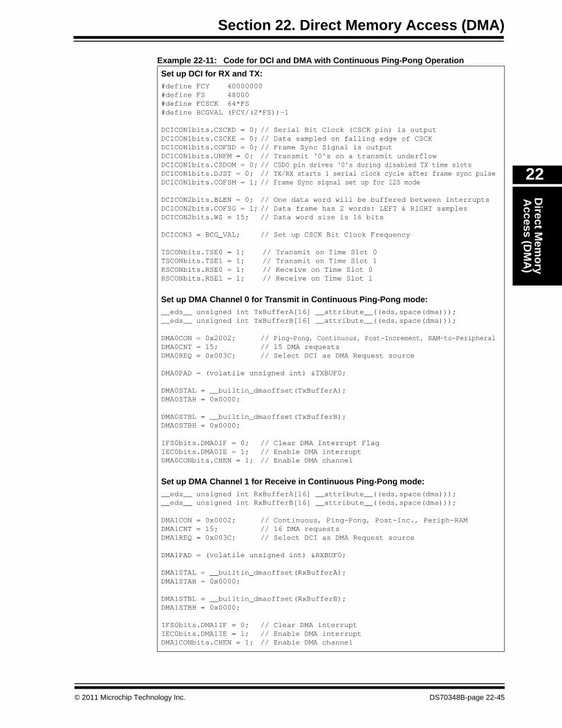
Section 22. Direct Memory Access (DMA)D
irect Mem
ory A
ccess (DM
A)
22
Example 22-11: Code for DCI and DMA with Continuous Ping-Pong OperationSet up DCI for RX and TX:#define FCY 40000000#define FS 48000#define FCSCK 64*FS#define BCGVAL (FCY/(2*FS))-1
DCICON1bits.CSCKD = 0; // Serial Bit Clock (CSCK pin) is outputDCICON1bits.CSCKE = 0; // Data sampled on falling edge of CSCKDCICON1bits.COFSD = 0; // Frame Sync Signal is outputDCICON1bits.UNFM = 0; // Transmit ‘0’s on a transmit underflowDCICON1bits.CSDOM = 0; // CSDO pin drives ‘0’s during disabled TX time slotsDCICON1bits.DJST = 0; // TX/RX starts 1 serial clock cycle after frame sync pulseDCICON1bits.COFSM = 1; // Frame Sync signal set up for I2S mode
DCICON2bits.BLEN = 0; // One data word will be buffered between interruptsDCICON2bits.COFSG = 1; // Data frame has 2 words: LEFT & RIGHT samplesDCICON2bits.WS = 15; // Data word size is 16 bits
DCICON3 = BCG_VAL; // Set up CSCK Bit Clock Frequency
TSCONbits.TSE0 = 1; // Transmit on Time Slot 0TSCONbits.TSE1 = 1; // Transmit on Time Slot 1RSCONbits.RSE0 = 1; // Receive on Time Slot 0RSCONbits.RSE1 = 1; // Receive on Time Slot 1
Set up DMA Channel 0 for Transmit in Continuous Ping-Pong mode:__eds__ unsigned int TxBufferA[16] __attribute__((eds,space(dma)));__eds__ unsigned int TxBufferB[16] __attribute__((eds,space(dma)));
DMA0CON = 0x2002; // Ping-Pong, Continuous, Post-Increment, RAM-to-PeripheralDMA0CNT = 15; // 15 DMA requestsDMA0REQ = 0x003C; // Select DCI as DMA Request source
DMA0PAD = (volatile unsigned int) &TXBUF0;
DMA0STAL = __builtin_dmaoffset(TxBufferA);DMA0STAH = 0x0000;
DMA0STBL = __builtin_dmaoffset(TxBufferB);DMA0STBH = 0x0000;
IFS0bits.DMA0IF = 0; // Clear DMA Interrupt FlagIEC0bits.DMA0IE = 1; // Enable DMA interruptDMA0CONbits.CHEN = 1; // Enable DMA channel
Set up DMA Channel 1 for Receive in Continuous Ping-Pong mode:__eds__ unsigned int RxBufferA[16] __attribute__((eds,space(dma)));__eds__ unsigned int RxBufferB[16] __attribute__((eds,space(dma)));
DMA1CON = 0x0002; // Continuous, Ping-Pong, Post-Inc., Periph-RAMDMA1CNT = 15; // 16 DMA requestsDMA1REQ = 0x003C; // Select DCI as DMA Request source
DMA1PAD = (volatile unsigned int) &RXBUF0;
DMA1STAL = __builtin_dmaoffset(RxBufferA);DMA1STAH = 0x0000;
DMA1STBL = __builtin_dmaoffset(RxBufferB);DMA1STBH = 0x0000;
IFS0bits.DMA1IF = 0; // Clear DMA interruptIEC0bits.DMA1IE = 1; // Enable DMA interruptDMA1CONbits.CHEN = 1; // Enable DMA channel
© 2011 Microchip Technology Inc. DS70348B-page 22-45

dsPIC33E/PIC24E Family Reference Manual
Example 22-11: Code for DCI and DMA with Continuous Ping-Pong Operation (Continued)
If One-Shot mode is selected while DMA is operating in Ping-Pong mode, DMA responds by reinitializing to point to the secondary buffer after transferring primary buffer, after which it transfers the secondary buffer. Subsequent block transfers will not occur, however, because the DMA channel disables itself. Figure 22-19 illustrates One-Shot data transfer in Ping-Pong mode.
Set up DMA Interrupt Handler:void __attribute__((__interrupt__,no_auto_psv)) _DMA0Interrupt(void){
static unsigned int TxBufferCount = 0; // Keep record of which buffer// has RX Data
if(BufferCount == 0) {
/* Notify application that TxBufferA has been transmitted */}else{/* Notify application that TxBufferB has been transmitted */}
BufferCount ^= 1;IFS0bits.DMA0IF = 0; // Clear the DMA0 Interrupt Flag
}
void __attribute__((__interrupt__,no_auto_psv)) _DMA1Interrupt(void){ static unsigned int RxBufferCount = 0; // Keep record of which buffer
// has RX Data
if(BufferCount == 0){/* Notify application that RxBufferA has been received */}else{/* Notify application that RxBufferB has been received */ }
BufferCount ^= 1;IFS0bits.DMA1IF = 0; // Clear the DMA1 Interrupt Flag
}
Enable DCI:/* Force first two words to fill-in TX buffer/shift register */DMA0REQbits.FORCE = 1;while(DMA0REQbits.FORCE == 1);
DMA0REQbits.FORCE = 1;while(DMA0REQbits.FORCE == 1);
DCICON1bits.DCIEN = 1; // Enable DCI
DS70348B-page 22-46 © 2011 Microchip Technology Inc.

Section 22. Direct Memory Access (DMA)D
irect Mem
ory A
ccess (DM
A)
22
Figure 22-19: Single Block Data Transfer in Ping-Pong Mode
22.6.10 Manual Transfer ModeFor peripherals that are sending data to memory using the DMA controller, the DMA data transfer starts automatically after the DMA channel and peripheral are initialized. When the peripheral is ready to move data to memory, it issues a DMA request. If data also needs to be sent to the peripheral at this time, the same DMA request can be used to activate another channel to read data from memory and write it to the peripheral.
In case, if the application only needs to send data to a peripheral (from a memory buffer), an initial (manual) data load into the peripheral may be required to start the process (see 22.7 “Starting DMA Transfers”). This process can be initiated with conventional software. However, a more convenient approach is to simply mimic the channel DMA request by setting a bit within the selected DMA channel. The DMA channel processes the forced request as it would with any other request and transfers the first data element to start the sequence. When the peripheral is ready for the next piece of data, it sends a normal DMA request and the DMA sends the next data element. This process is illustrated in Figure 22-20.
A manual DMA request can be created by setting the FORCE bit in the DMA Channel x IRQ Select register (DMAxREQ). Once set, the FORCE bit can not be cleared by the user application. It must be cleared by hardware when the forced DMA transfer is complete. Depending on when the FORCE bit is set, these special conditions apply:
• Setting the FORCE bit while the DMA transfer is in progress has no effect and is ignored.• Setting the FORCE bit while channel x is being configured (i.e., setting the FORCE bit during
the same write that configures the DMA channel) can result in unpredictable behavior and should be avoided.
• Setting the FORCE bit will cause the DMA transfer count to be decremented by 1. This has to be taken into account by the user software when handling the first block of data transferred using DMA.
• An attempt to set the FORCE bit while a peripheral interrupt request is pending (for this channel) is discarded in favor of the interrupt-based request. However, an error condition is generated by setting the Channel x Collision Flag bit (RQCOLx) in the DMA Request Collision Status register (DMARQC). See 22.10 “Data Write and Request Collisions” for more details.
Note: Setting the FORCE bit during the same write that configures the DMA channel may result in unpredictable behavior and should be avoided.
Transfer #1Transfer #2Transfer #3
Transfer #n
CO
UN
T++
DMAxSTA
COUNT=0
COUNT = DMAxCNT+1
CPU Block Transfer, Complete IRQTransfer #1Transfer #2Transfer #3
Transfer #n
CO
UN
T++
DMAxSTB
COUNT = DMAxCNT+1
CPU Block Transfer Complete IRQ, Disable DMA Channel
Buffer A (Primary)
Buffer B (Secondary)
© 2011 Microchip Technology Inc. DS70348B-page 22-47

dsPIC33E/PIC24E Family Reference Manual
Figure 22-20: Data Transfer Initiated in Manual Mode
22.6.11 Null Data Write ModeNull Data Write mode is the most useful mode in applications in which sequential reception of data is required without any data transmission like SPI.
SPI is essentially a simple shift register, clocking a bit of data in and out for each clock period. However, an unusual situation arises when SPI is configured in Master mode (i.e., when SPI is to be the source of the clock) but only received data is of interest. In this case, something must be written to the SPI data register in order to start the SPI data clock and to receive the external data.
It would be possible to allocate two DMA channels, one for data reception and the other to simply feed null, or zero, data into the SPI. However, a more efficient solution is to use a DMA Null Data Write mode that automatically writes a null value to the SPI data register after each data element has been received and transferred by the DMA channel configured for peripheral data reads.
If the Null Data Peripheral Write Mode Select bit (NULLW) is set in the DMA Channel x Control register (DMAxCON), and the DMA channel is configured to read from the peripheral, then the DMA channel also executes a null (all zeros) write to the peripheral address in the same cycle as the peripheral data read. This write occurs across the peripheral bus concurrently with the (data) write to the DPSRAM/RAM. Figure 22-21 illustrates this mode.
During normal operation in this mode, the Null Data Write can only occur in response to a peripheral DMA request (i.e., after data has been received and is available for transfer). An initial CPU write to the peripheral is required to start reception of the first word, after which DMA takes care of all subsequent peripheral (null) data writes. That is, the CPU null write starts the SPI (master) sending/receiving data, which in turn eventually generates a DMA request to move the newly received data.
Alternatively, a forced DMA transfer could be used to ‘kick start’ the process. However, this will also include a redundant peripheral read (data not valid) and an associated memory pointer adjustment, which must be taken into account.
DMA3STA DMA3STA + 1DMA3STA + 2
Data 0
Peripheral 1
DMAChannel 6
First Transfer ForcedA
DMA3STA DMA3STA + 1DMA3STA + 2
Data 0Data 1
Peripheral 1
DMAChannel 6
Subsequent Transfers Requested by PeripheralB
CPU Write toFORCE Bit
Data 1Data 2
Data 2
Transfer 1
Transfer 2Transfer 3
DMA Request
DS70348B-page 22-48 © 2011 Microchip Technology Inc.

Section 22. Direct Memory Access (DMA)D
irect Mem
ory A
ccess (DM
A)
22
Figure 22-21: Data Transfer with Null Data Write Mode
Example 22-12: SPI and DMA with Null Data Write Mode
DMA3STA DMA3STA + 1DMA3STA + 2
Data 0Data 1
SPI DMA
Channel 1
Data 2
Transfer 2Transfer 3
Transfer 1TX
RX
Null Data Writes generated by DMA
Data Transfer
Set up SPI for Master mode:SPI1CON1bits.MODE16 = 1; // Communication is word-wide (16 bits)SPI1CON1bits.MSTEN = 1; // Master mode enabledSPI1STATbits.SPIEN = 1; // Enable SPI module
Set up DMA Channel 1 for Null Data Write mode:unsigned int BufferA[16];unsigned int BufferB[16];
DMA1CON = 0x0802; // Null Write, Continuous, Ping-Pong,// Post-Increment, Periph-to-RAM
DMA1CNT = 15; // Transfer 16 words at a timeDMA1REQ = 0x000A; // Select SPI1 as DMA Request source
DMA1STAL = &BufferA; // The buffer is in non-DMA RAM areaDMA1STAH = 0x0000;
DMA1STBL = &BufferB; // The buffer is in non-DMA RAM areaDMA1STBH = 0x0000;
DMA1PAD = (volatile unsigned int) &SPI1BUF;
IFS0bits.DMA1IF = 0;IEC0bits.DMA1IE = 1; // Enable DMA interruptDMA1CONbits.CHEN = 1; // Enable DMA channel
DMA1REQbits.FORCE = 1; // Force first word after enabling SPI
Set up DMA Interrupt Handler:void __attribute__((__interrupt__,no_auto_psv)) _DMA1Interrupt(void){ static unsigned int BufferCount = 0; // Keep record of which buffer
// contains RX data
if(BufferCount == 0){ProcessRxData(BufferA); // Process received SPI data in
// DMA RAM Primary buffer}else{ProcessRxData(BufferB); // Process received SPI data in
// DMA RAM Secondary buffer}
BufferCount ^= 1;IFS0bits.DMA1IF = 0; // Clear the DMA1 Interrupt Flag
}
© 2011 Microchip Technology Inc. DS70348B-page 22-49

dsPIC33E/PIC24E Family Reference Manual
22.7 STARTING DMA TRANSFERSBefore DMA transfers can begin, the DMA channel must be enabled by setting the CHEN bit to ‘1’ in the DMAxCON register. When the DMA channel is active, it can be reinitialized by disabling this channel (CHEN = 0), followed by re-enabling it (CHEN = 1). This process resets the DMA transfer count to zero and sets the active DMA buffer to the primary buffer.When the DMA channel and peripheral are properly initialized, the DMA transfer starts as soon as the peripheral is ready to move data and issues a DMA request. However, some peripherals may not issue a DMA request (and therefore will not start the DMA transfer) until certain conditions exist. In these cases, a combination of different DMA modes and procedures may need to be applied to initiate the DMA transfer:
22.7.1 Starting DMA with the Serial Peripheral Interface (SPI)Starting the DMA transfer to/from the SPI peripheral depends upon the SPI data direction and Slave or Master mode:
• TX only in Master mode – In this configuration, no DMA request is issued until the first block of SPI data is sent. To initiate DMA transfers, the user application must first send data using the DMA Manual Transfer mode, or it must first write data into the SPI buffer (SPIxBUF) independently of DMA.
• RX only in Master mode – In this configuration, no DMA request is issued until the first block of SPI data is received. However, in Master mode, no data is received until SPI transmits first. To initiate DMA transfers, the user application must use DMA Null Data Write mode, and start DMA Manual Transfer mode.
• RX and TX in Master mode – In this configuration, no DMA request is issued until the first block of SPI data is received. However, in Master mode, no data is received until the SPI transmits it. To initiate DMA transfers, the user application must first send data using the DMA Manual Transfer mode, or it must first write data into the SPI buffer (SPIxBUF) independently of DMA.
• TX only in Slave mode – In this configuration, no DMA request is issued until the first block of SPI data is received. To initiate DMA transfers, the user application must first send data using the DMA Manual Transfer mode, or it must first write data into the SPI buffer (SPIxBUF) independently of DMA.
• RX only in Slave mode – This configuration generates a DMA request as soon as the first SPI data has arrived, so no special steps need to be taken by the user to initiate DMA transfers.
• RX and TX in Slave mode – In this configuration, no DMA request is issued until the first SPI data block is received. To initiate DMA transfers, the user application must first send data utilizing the DMA Manual Transfer mode, or it must first write data into the SPI buffer (SPIxBUF) independently of DMA.
22.7.2 Starting DMA with the Data Converter Interface (DCI)Unlike other serial peripherals, DCI starts transmitting as soon as it is enabled (assuming it is the Master). It constantly feeds synchronous frames of data to the external codec to which it is connected. Before enabling DCI the user must:• Configure DCI as described in 22.5.2 “Peripheral Configuration Setup”• If connected to a stereo codec, use DMA Manual Transfer mode to initiate the first two data
transfers- Set the FORCE bit in the DMAxREQ register to transfer the DCI left channel sample- Set the FORCE bit for the second time to transfer the DCI right channel sample
After these steps are completed, enable the DCI peripheral (see Example 22-11).
22.7.3 Starting DMA with the UARTThe UART receiver issues a DMA request as soon as data is received. No special steps need to be taken by the user application to initiate DMA transfers. The UART transmitter issues a DMA request as soon as the UART and transmitter are enabled. This means that the DMA channel and buffers must be initialized and enabled before the UART and transmitter. Ensure that the UART is configured as described in Table 22-2.Alternatively, the UART and UART transmitter can be enabled before the DMA channel is enabled. In this case, the UART transmitter DMA request is lost, and the user application must issue a DMA request to start DMA transfers by setting the FORCE bit in the DMAxREQ register.
DS70348B-page 22-50 © 2011 Microchip Technology Inc.

Section 22. Direct Memory Access (DMA)D
irect Mem
ory A
ccess (DM
A)
22
22.8 DMA CHANNEL ARBITRATION AND OVERRUNSEach DMA channel has a fixed priority. Channel 0 is the highest, and Channel 7 is the lowest. When a DMA transfer is requested by the source, the request is latched by the associated DMA channel. The DMA controller acts as an arbitrator. If no other transfer is underway or pending, the controller grants bus resources to the requesting DMA channel. The DMA controller ensures that no other DMA channel is granted any resource until the current DMA channel completes its operation.
If multiple DMA requests arrive or are pending, the priority logic within the DMA controller grants resources to the highest priority DMA channel for completing its operation. All other DMA requests remain pending until the selected DMA transfer is complete. If another DMA request arrives while the current DMA transfer is underway, it is also prioritized with any pending DMA requests, ensuring that the highest priority request is always serviced after the current DMA transfer has completed.
If the DMA channel is trying to access memory outside of DPSRAM, and the memory arbiter cannot grant access, the DMA channel will be stalled until the arbiter acknowledges the request, thereby granting access. Consequently, it should be noted that all subsequent DMA channel requests, regardless of their priority relative to the stalled channel, will also remain pending until the arbiter resolves the outstanding request.
As the DMA channels are prioritized, it is possible that a DMA request will not be immediately serviced and will become pending. The request will remain pending until all higher priority channels have been serviced. If another interrupt arrives before the DMA controller has cleared the original DMA request, and the interrupt is the same type as the pending interrupt, a data overrun occurs.
A data overrun is defined as the condition where new data has arrived in a peripheral data buffer before DMA could move the prior data. Some DMA-ready peripherals can detect data overruns and issue a CPU interrupt (if the corresponding peripheral error interrupt is enabled), as shown in Table 22-3.
Table 22-3: Overrun Handling by DMA-Ready Peripherals
DMA-Ready Peripheral Data Overrun Handling
Serial Peripheral Interface (SPI) Data waiting to be moved by the DMA channel is not overwritten by additional incoming data. Subsequent incoming data is lost, and the SPI Receive Overflow bit (SPIROV) is set in the SPI Status register (SPIxSTAT). Additionally, the SPIx Fault interrupt is generated if the SPI Error Interrupt Enable bit (SPIxEIE) is set in the Interrupt Enable Control register (IECx) in the interrupt controller.
Universal Asynchronous Receiver Transmitter (UART)
Data waiting to be moved by the DMA channel is not overwritten by additional incoming data. Subsequent incoming data is lost, and the Overflow Error bit (OERR) is set in the UART Status register (UxSTA). Also, the UARTx Error interrupt is generated if the UART Error Interrupt Enable bit (UxEIE) is set in the Interrupt Enable Control register (IECx) in the interrupt controller.
Data Converter Interface (DCI) Data waiting to be moved by the DMA channel is overwritten by additional incoming data, and the Receive Overflow bit (ROV) is set in the DCI Status register (DCISTAT). Additionally, the DCI Fault interrupt is generated if the DCI Error Interrupt Enable bit (DCIEIE) is set in the Interrupt Enable Control register (IEC0) in the interrupt controller.
10-bit/12-bit Analog-to-Digital Converter (ADC)
Data waiting to be moved by the DMA channel is overwritten by additional incoming data. The overrun condition is not detected by the ADC.
Other DMA-Ready Peripherals No data overrun can occur.
© 2011 Microchip Technology Inc. DS70348B-page 22-51

dsPIC33E/PIC24E Family Reference Manual
Data overruns are only detectable in hardware when the DMA is moving data from a peripheral to memory. DMA data transfers from memory to a peripheral (based on, for example, a buffer empty interrupt) will always execute. Any consequential memory overruns must be detected using software. The duplicate DMA request is ignored and the pending request remains pending. As usual, the DMA channel clears the DMA request when the transfer is eventually completed. If the CPU does not intervene in the meantime, the data transferred will be the latest (overrun) data, and the prior data will be lost.
The user application can handle an overrun error in different ways, depending on the nature of the data source. Data recovery and resynchronization of the DMAC with its data source/sink is a task that is highly application dependent. For streaming data, such as that from a CODEC (via the DCI peripheral), the application can ignore the lost data. After fixing the source of the problem (if possible), the DMA interrupt handler should attempt to resynchronize the DMAC and DCI so that data is again buffered correctly. The user application should react fast enough to prevent any further overruns from occurring.
By the time the peripheral overrun interrupt is entered, the pending DMA request will have already moved the overrun data value to the address where the lost data should have gone. That data can be moved to its correct address, and a null data value inserted into the missing data slot. The memory address of the channel can then be adjusted accordingly. Subsequent DMA requests to the faulted channel then initiate transfers as normal to the corrected memory address. For applications where the data cannot be lost, the peripheral overrun interrupt will need to abort the current block transfer, reinitialize the DMA channel and request a data resend before it is lost.
DS70348B-page 22-52 © 2011 Microchip Technology Inc.

Section 22. Direct Memory Access (DMA)D
irect Mem
ory A
ccess (DM
A)
22
22.9 DEBUGGING SUPPORTTo improve user visibility into DMA operation during debugging, the DMA controller includes several status registers that can provide information on which DMA channel executed last (LSTCH<3:0> bits in the DMALCA register), which memory address offset it was accessing (DSADR<21:0> bits in the DSADR register) and from which buffer (PPSTx bits in the DMAPPS register).
22.10 DATA WRITE AND REQUEST COLLISIONS
22.10.1 Data Write CollisionsThe CPU and DMA channel may simultaneously read or read/write to any DPSRAM or DMA-ready peripheral data register. The only constraint is that the CPU and DMA channel should not simultaneously write to the same address. Under normal circumstances, this situation should never arise. However, if for some reason it does, then it will be detected and the CPU write will also be allowed to take priority, though that is mainly to provide predictable behavior and is otherwise of little practical consequence.
It is also permissible for the DMA channel to write to a location during the same bus cycle that the CPU is reading it, and vice versa. However, it should be noted that the resultant reads are of the old data, not the data written during that bus cycle. Also note that this situation is consideredas a normal operation and does not result in any special action being taken.
In the event of a simultaneous write to the same peripheral address by the CPU and DMA channel, the PWCOLx bit is set in the DMA Peripheral Write Collision Status register (DMAPWC).All collision status flags are logically read together to generate a common DMAC Fault trap. The PWCOLx flags are automatically cleared when the user application clears the DMAC Error Status bit (DMACERR) in the Interrupt Controller register (INTCON1).
Subsequent DMA requests to a channel that has a write collision error are ignored while PWCOLx remains set.
Table 22-4 summarizes various concurrent events and how they are handled by the device.
Table 22-4: Dual-Ported Element Concurrent Access Rules
Example 22-13 illustrates DMA controller trap handling with DMA Channel 0 transferring data from the DPSRAM to the peripheral (UART), and DMA Channel 1 transferring data from the peripheral (ADC) to the DPSRAM.
Access Type CPU Action DMA Read DMA Write Comment
DPSRAM Concurrent
Access
CPU Read OK — Concurrent CPU and DMA reads allowed
CPU Read — OK DMA will overwrite data read by CPU
CPU Write OK — CPU will overwrite data read by DMA
CPU Write — CPU prevails DMA write ignored
SFR Concurrent
Access
CPU Read OK — Concurrent CPU and DMA reads allowed
CPU Read — OK DMA will overwrite data read by CPU
CPU Write OK — CPU will overwrite data read by DMA
CPU Write — CPU prevails DMA write ignored; PWCOLx flag set
© 2011 Microchip Technology Inc. DS70348B-page 22-53

dsPIC33E/PIC24E Family Reference Manual
Example 22-13: DMA Controller Trap Handling
22.10.2 Channel Request CollisionsIf a valid interrupt-based DMA request is underway, pending or arrives coincident with a manually initiated transfer (FORCE = 1) to the same channel, the manual request is generally discarded (ignored) in favor of the interrupt-based request. When detected, request collisions set corresponding flags (RQCOLx) in the DMA Request Collision register (DMARQC).
Because DMA transfers could be multi-cycle events, user-forced and interrupt-based transfer requests can arrive at different times relative to each other and still result in a request collision. This means a collision is defined as any cycle during which forced and interrupt-based transfer requests overlap. Request collisions are handled as follows:
1. In the event of a collision where the interrupt-based request and the setting of the FORCE bit occur coincidentally, the FORCE request is discarded, the FORCE bit is automatically cleared, and the corresponding RQCOL bit is set. The interrupt based request is allowed to proceed.
2. In the event of a collision where the interrupt-based request has already initiated the transfer and the FORCE bit is subsequently set, the FORCE request is discarded, the FORCE bit is automatically cleared, and the corresponding RQCOL bit is set. The interrupt based request is allowed to proceed.
3. In the event of a collision where the FORCE request has already initiated the transfer and it arrived before the interrupt-based request occurred, the FORCE request is allowed to proceed, but the interrupt-based request will be left pending until the FORCE request has completed. The FORCE bit is automatically cleared and the corresponding RQCOL bit is set. The interrupt-based request will then be executed.
void __attribute__((__interrupt__,no_auto_psv)) _DMACError(void){
static unsigned int ErrorLocation;
// Peripheral Write Collision Error Locationif(DMACS0 & 0x0100){
ErrorLocation = DMA0STA;}
// DMA RAM Write Collision Error Locationif(DMACS0 & 0x0002){
ErrorLocation = DMA1STA;}
DMACS0 = 0; //Clear Write Collision FlagINTCON1bits.DMACERR = 0; //Clear Trap Flag
}
DS70348B-page 22-54 © 2011 Microchip Technology Inc.

Section 22. Direct Memory Access (DMA)D
irect Mem
ory A
ccess (DM
A)
22
22.11 OPERATION IN POWER-SAVING MODES
22.11.1 Sleep ModeThe DMA is disabled during the Sleep power-saving mode. Prior to entering Sleep mode, it is recommended (though not essential) that all DMA channels either be allowed to complete the block transfer that is currently underway, or be disabled.
22.11.2 Idle ModeDMA is a second bus master within the system and can, therefore, continue to transfer data when the CPU has entered the Idle power-saving mode. Provided that the peripheral being serviced by the DMA channel is configured for operation during Idle mode, data may be transferred to and from the peripheral and memory. When the block transfer is complete, the DMA channel issues an interrupt (if enabled) and wakes up the CPU. The CPU then runs the interrupt service handler.
Each peripheral includes a Stop in Idle control bit. When set, the control bit disables the peripheral while the CPU is in Idle mode. If the DMA is being used to transfer data in and/or out of the peripheral, engaging the Stop in Idle feature within the peripheral will, in effect, also disable the DMA channel associated with the peripheral.
© 2011 Microchip Technology Inc. DS70348B-page 22-55

dsPIC33E/PIC
24E Family R
eference Manual
DS
70348B-page 22-56
© 2011 M
icrochip Technology Inc.
ble 22-5.
Bit 3 Bit 2 Bit 1 Bit 0 All Resets
— — MODE<1:0> 0000
SEL<7:0> 0000
A<23:16> 0000
0000
B<23:16> 0000
0000
0000
0000
0000
L4 PWCOL3 PWCOL2 PWCOL1 PWCOL0 0000
L4 RQCOL3 RQCOL2 RQCOL1 RQCOL0 0000
LSTCH<3:0> 000F
4 PPST3 PPST2 PPST1 PPST0 0000
22.12 REGISTER MAPA summary of the registers associated with the dsPIC33E/PIC24E Direct Memory Access (DMA) module is provided in Ta
Table 22-5: DMA Register Map
File Name Bit 15 Bit 14 Bit 13 Bit 12 Bit 11 Bit 10 Bit 9 Bit 8 Bit 7 Bit 6 Bit 5 Bit 4
DMAxCON CHEN SIZE DIR HALF NULLW — — — — — AMODE<1:0>DMAxREQ FORCE — — — — — — — IRQDMAxSTAH — — — — — — — — STDMAxSTAL STA<15:0>DMAxSTBH — — — — — — — — STDMAxSTBL STB<15:0>DMAxPAD PAD<15:0>DMAxCNT CNT<15:0>DSADR DSADR<15:0>DMAPWC — PWCOL14 PWCOL13 PWCOL12 PWCOL11 PWCOL10 PWCOL9 PWCOL8 PWCOL7 PWCOL6 PWCOL5 PWCODMARQC — RQCOL14 RQCOL13 RQCOL12 RQCOL11 RQCOL10 RQCOL9 RQCOL8 RQCOL7 RQCOL6 RQCOL5 RQCODMALCA — — — — — — — — — — — —DMAPPS — PPST14 PPST13 PPST12 PPST11 PPST10 PPST9 PPST8 PPST7 PPST6 PPST5 PPSTLegend: — = unimplemented, read as ‘0’. Reset values are shown in hexadecimal.

Section 22. Direct Memory Access (DMA)D
irect Mem
ory A
ccess (DM
A)
22
22.13 RELATED APPLICATION NOTESThis section lists application notes that are related to the use of Direct Memory Access. These application notes may not be written specifically for the dsPIC33E/PIC24E device family, but the concepts are pertinent and could be used with modification and possible limitations. The current application notes related to the Direct Memory Access (DMA) module include:
Title Application NoteNo related application notes at this time. N/A
Note: Please visit the Microchip web site (www.microchip.com) for additional Application Notes and code examples for the dsPIC33E/PIC24E family of devices.
© 2011 Microchip Technology Inc. DS70348B-page 22-57
dsPIC33E/PIC24E Family Reference Manual
22.14 REVISION HISTORY
Revision A (April 2009)This is the initial released version of this document.
Revision B (May 2011)This revision includes the following changes:
• Examples:- Updated the code in Example 22-2 through Example 22-13
• Figures:- Updated Figure 22-4 through Figure 22-6- Updated the figure title in Figure 22-6- Added Figure 22-7
• Notes:- Added a note in Figure 22-6
• Registers:- Changed the characteristic of bit 15 and bit 14 from R/W-0 to U-0 in Register 22-8- Renamed the RQCOLx bit name from Channel x Peripheral Write Collision Flag bit to
Channel x Transfer Request Collision Flag bit in Register 22-11• Sections:
- Updated 22.5.3 “Memory Address Initialization”- Updated the special conditions that are applicable for the FORCE bit depending on
when the FORCE bit is set, in 22.6.10 “Manual Transfer Mode”• Tables:
- Updated the configuration considerations of UART in Table 22-2• Any references to (SMPI<3:0>) is updated to (SMPI<4:0>)• Updated the Family Reference Manual name dsPIC33E to dsPIC33E/PIC24E Family
Reference Manual• Additional minor corrections such as language and formatting updates were incorporated
throughout the document
DS70348B-page 22-58 © 2011 Microchip Technology Inc.

Note the following details of the code protection feature on Microchip devices:• Microchip products meet the specification contained in their particular Microchip Data Sheet.
• Microchip believes that its family of products is one of the most secure families of its kind on the market today, when used in the intended manner and under normal conditions.
• There are dishonest and possibly illegal methods used to breach the code protection feature. All of these methods, to our knowledge, require using the Microchip products in a manner outside the operating specifications contained in Microchip’s Data Sheets. Most likely, the person doing so is engaged in theft of intellectual property.
• Microchip is willing to work with the customer who is concerned about the integrity of their code.
• Neither Microchip nor any other semiconductor manufacturer can guarantee the security of their code. Code protection does not mean that we are guaranteeing the product as “unbreakable.”
Code protection is constantly evolving. We at Microchip are committed to continuously improving the code protection features of our products. Attempts to break Microchip’s code protection feature may be a violation of the Digital Millennium Copyright Act. If such acts allow unauthorized access to your software or other copyrighted work, you may have a right to sue for relief under that Act.
Information contained in this publication regarding device applications and the like is provided only for your convenience and may be superseded by updates. It is your responsibility to ensure that your application meets with your specifications. MICROCHIP MAKES NO REPRESENTATIONS OR WARRANTIES OF ANY KIND WHETHER EXPRESS OR IMPLIED, WRITTEN OR ORAL, STATUTORY OR OTHERWISE, RELATED TO THE INFORMATION, INCLUDING BUT NOT LIMITED TO ITS CONDITION, QUALITY, PERFORMANCE, MERCHANTABILITY OR FITNESS FOR PURPOSE. Microchip disclaims all liability arising from this information and its use. Use of Microchip devices in life support and/or safety applications is entirely at the buyer’s risk, and the buyer agrees to defend, indemnify and hold harmless Microchip from any and all damages, claims, suits, or expenses resulting from such use. No licenses are conveyed, implicitly or otherwise, under any Microchip intellectual property rights.
© 2011 Microchip Technology Inc.
Trademarks
The Microchip name and logo, the Microchip logo, dsPIC, KEELOQ, KEELOQ logo, MPLAB, PIC, PICmicro, PICSTART, PIC32 logo, rfPIC and UNI/O are registered trademarks of Microchip Technology Incorporated in the U.S.A. and other countries.
FilterLab, Hampshire, HI-TECH C, Linear Active Thermistor, MXDEV, MXLAB, SEEVAL and The Embedded Control Solutions Company are registered trademarks of Microchip Technology Incorporated in the U.S.A.
Analog-for-the-Digital Age, Application Maestro, CodeGuard, dsPICDEM, dsPICDEM.net, dsPICworks, dsSPEAK, ECAN, ECONOMONITOR, FanSense, HI-TIDE, In-Circuit Serial Programming, ICSP, Mindi, MiWi, MPASM, MPLAB Certified logo, MPLIB, MPLINK, mTouch, Omniscient Code Generation, PICC, PICC-18, PICDEM, PICDEM.net, PICkit, PICtail, REAL ICE, rfLAB, Select Mode, Total Endurance, TSHARC, UniWinDriver, WiperLock and ZENA are trademarks of Microchip Technology Incorporated in the U.S.A. and other countries.
SQTP is a service mark of Microchip Technology Incorporated in the U.S.A.
All other trademarks mentioned herein are property of their respective companies.
© 2011, Microchip Technology Incorporated, Printed in the U.S.A., All Rights Reserved.
Printed on recycled paper.
ISBN: 978-1-61341-161-2
DS70348B-page 22 -59
Microchip received ISO/TS-16949:2002 certification for its worldwide headquarters, design and wafer fabrication facilities in Chandler and Tempe, Arizona; Gresham, Oregon and design centers in California and India. The Company’s quality system processes and procedures are for its PIC® MCUs and dsPIC® DSCs, KEELOQ® code hopping devices, Serial EEPROMs, microperipherals, nonvolatile memory and analog products. In addition, Microchip’s quality system for the design and manufacture of development systems is ISO 9001:2000 certified.

DS70348B-page 22-60 © 2011 Microchip Technology Inc.
AMERICASCorporate Office2355 West Chandler Blvd.Chandler, AZ 85224-6199Tel: 480-792-7200 Fax: 480-792-7277Technical Support: http://www.microchip.com/supportWeb Address: www.microchip.comAtlantaDuluth, GA Tel: 678-957-9614 Fax: 678-957-1455BostonWestborough, MA Tel: 774-760-0087 Fax: 774-760-0088ChicagoItasca, IL Tel: 630-285-0071 Fax: 630-285-0075ClevelandIndependence, OH Tel: 216-447-0464 Fax: 216-447-0643DallasAddison, TX Tel: 972-818-7423 Fax: 972-818-2924DetroitFarmington Hills, MI Tel: 248-538-2250Fax: 248-538-2260IndianapolisNoblesville, IN Tel: 317-773-8323Fax: 317-773-5453Los AngelesMission Viejo, CA Tel: 949-462-9523 Fax: 949-462-9608Santa ClaraSanta Clara, CA Tel: 408-961-6444Fax: 408-961-6445TorontoMississauga, Ontario, CanadaTel: 905-673-0699 Fax: 905-673-6509
ASIA/PACIFICAsia Pacific OfficeSuites 3707-14, 37th FloorTower 6, The GatewayHarbour City, KowloonHong KongTel: 852-2401-1200Fax: 852-2401-3431Australia - SydneyTel: 61-2-9868-6733Fax: 61-2-9868-6755China - BeijingTel: 86-10-8569-7000 Fax: 86-10-8528-2104China - ChengduTel: 86-28-8665-5511Fax: 86-28-8665-7889China - ChongqingTel: 86-23-8980-9588Fax: 86-23-8980-9500China - HangzhouTel: 86-571-2819-3180 Fax: 86-571-2819-3189China - Hong Kong SARTel: 852-2401-1200 Fax: 852-2401-3431China - NanjingTel: 86-25-8473-2460Fax: 86-25-8473-2470China - QingdaoTel: 86-532-8502-7355Fax: 86-532-8502-7205China - ShanghaiTel: 86-21-5407-5533 Fax: 86-21-5407-5066China - ShenyangTel: 86-24-2334-2829Fax: 86-24-2334-2393China - ShenzhenTel: 86-755-8203-2660 Fax: 86-755-8203-1760China - WuhanTel: 86-27-5980-5300Fax: 86-27-5980-5118China - XianTel: 86-29-8833-7252Fax: 86-29-8833-7256China - XiamenTel: 86-592-2388138 Fax: 86-592-2388130China - ZhuhaiTel: 86-756-3210040 Fax: 86-756-3210049
ASIA/PACIFICIndia - BangaloreTel: 91-80-3090-4444 Fax: 91-80-3090-4123India - New DelhiTel: 91-11-4160-8631Fax: 91-11-4160-8632India - PuneTel: 91-20-2566-1512Fax: 91-20-2566-1513Japan - YokohamaTel: 81-45-471- 6166 Fax: 81-45-471-6122Korea - DaeguTel: 82-53-744-4301Fax: 82-53-744-4302Korea - SeoulTel: 82-2-554-7200Fax: 82-2-558-5932 or 82-2-558-5934Malaysia - Kuala LumpurTel: 60-3-6201-9857Fax: 60-3-6201-9859Malaysia - PenangTel: 60-4-227-8870Fax: 60-4-227-4068Philippines - ManilaTel: 63-2-634-9065Fax: 63-2-634-9069SingaporeTel: 65-6334-8870Fax: 65-6334-8850Taiwan - Hsin ChuTel: 886-3-6578-300Fax: 886-3-6578-370Taiwan - KaohsiungTel: 886-7-213-7830Fax: 886-7-330-9305Taiwan - TaipeiTel: 886-2-2500-6610 Fax: 886-2-2508-0102Thailand - BangkokTel: 66-2-694-1351Fax: 66-2-694-1350
EUROPEAustria - WelsTel: 43-7242-2244-39Fax: 43-7242-2244-393Denmark - CopenhagenTel: 45-4450-2828 Fax: 45-4485-2829France - ParisTel: 33-1-69-53-63-20 Fax: 33-1-69-30-90-79Germany - MunichTel: 49-89-627-144-0 Fax: 49-89-627-144-44Italy - Milan Tel: 39-0331-742611 Fax: 39-0331-466781Netherlands - DrunenTel: 31-416-690399 Fax: 31-416-690340Spain - MadridTel: 34-91-708-08-90Fax: 34-91-708-08-91UK - WokinghamTel: 44-118-921-5869Fax: 44-118-921-5820
Worldwide Sales and Service
05/02/11