Embed Size (px)
Citation preview

ECA
N™
21
Section 21. ECAN™
HIGHLIGHTSThis section of the manual contains the following major topics:
21.1 Introduction .................................................................................................................. 21-221.2 CAN Message Formats................................................................................................ 21-421.3 ECAN Registers........................................................................................................... 21-921.4 ECAN Message Buffers ............................................................................................. 21-3021.5 ECAN Operating Modes ............................................................................................ 21-3421.6 Transmitting ECAN Messages................................................................................... 21-3521.7 Receiving ECAN Messages....................................................................................... 21-4121.8 DMA Controller Configuration .................................................................................... 21-5321.9 Bit Timing ................................................................................................................... 21-5621.10 ECAN Error Management .......................................................................................... 21-6021.11 ECAN Interrupts......................................................................................................... 21-6321.12 ECAN Low-Power Modes .......................................................................................... 21-6621.13 ECAN Time Stamping Using Input Capture ............................................................... 21-6621.14 Register Maps............................................................................................................ 21-6621.15 Related Application Notes.......................................................................................... 21-7321.16 Revision History ......................................................................................................... 21-74
© 2007-2012 Microchip Technology Inc. DS70185C-page 21-1

dsPIC33F/PIC24H Family Reference Manual
21.1 INTRODUCTIONThe dsPIC33F/PIC24H Enhanced Controller Area Network (ECAN™) module implements theCAN Protocol 2.0B, used primarily in industrial and automotive applications. This asynchronousserial data communication protocol provides reliable communications in electrically noisyenvironments. The dsPIC33F device family integrates up to two ECAN modules. Figure 21-1illustrates a typical CAN bus topology.
Figure 21-1: Typical CAN Bus Network
The ECAN module supports the following key features:
Standards Compliance:• Full CAN 2.0B compliance• Programmable bit rate up to 1 Mbps
Message Reception:• 32 message buffers – all of them can be used for reception• 16 acceptance filters for message filtering• Three acceptance filter mask registers for message filtering• Automatic response to Remote Transmit Request• Up to 32-message deep First In First Out (FIFO) buffer• DeviceNet™ addressing support• DMA interface for message reception
Note: This family reference manual section is meant to serve as a complement to devicedata sheets. Depending on the device variant, this manual section may not apply toall dsPIC33F/PIC24H devices.
Please consult the note at the beginning of the “Direct Memory Access (DMA)”chapter in the current device data sheet to check whether this document supportsthe device you are using.
Device data sheets and family reference manual sections are available fordownload from the Microchip Worldwide Web site at: http://www.microchip.com
CANbus
ECAN1
PIC® MCUwith Integrated
ECAN
CANTransceiver
dsPIC33F/PIC24Hwith Integrated
ECAN™
dsPIC30Fwith Integrated
CAN
TransceiverCAN
TransceiverCAN
TransceiverCAN
ECAN2
CANTransceiver
dsPIC33F/PIC24H
DS70185C-page 21-2 © 2007-2012 Microchip Technology Inc.
Section 21. ECAN™EC
AN
™
21
Message Transmission:• Eight message buffers configurable for message transmission • User-defined priority levels for message buffers used for transmission• DMA interface for message transmissionOthers:• Loopback, Listen All Messages, and Listen Only modes for self-test, system diagnostics,
and bus monitoring• Low-power operating modes
Figure 21-2 illustrates the general structure of the ECAN module and its interaction with the DMAController and DMA RAM.
Figure 21-2: ECAN™ Interaction with DMA
21.1.1 ECAN ModuleThe ECAN module consists of a protocol engine, message acceptance filters, and separatetransmit and receive DMA interfaces. The protocol engine transmits and receives messages toand from the CAN bus (as per CAN bus 2.0B protocol). The user-configurable acceptance filtersare used by the module to examine the received message to determine if it should be stored inthe DMA message buffer or discarded.
For received messages, the receive DMA interface generates a receive data interrupt to initiatea DMA cycle. The receive DMA channel reads data from the CiRXD register and writes it into themessage buffer.
For transmit messages, the transmit DMA interface generates a transmit data interrupt to start aDMA cycle. The transmit DMA channel reads from the message buffer and writes to the CiTXDregister for message transmission.
21.1.2 Message BuffersThe ECAN module supports up to 32 message buffers for storing data transmitted or received onthe CAN bus. These buffers are located in DMA RAM. Message buffers 0-7 can be configuredfor either transmit or receive operation. Message buffers 8-31 are receive-only buffers and cannot be used for Message Transmission.
21.1.3 DMA ControllerThe DMA controller acts as an interface between the message buffers and ECAN to transfer databack and forth without CPU intervention. The DMA controller supports up to eight channels fortransferring data between DMA RAM and the dsPIC33F peripherals. Two separate DMAchannels are needed to support CAN message transmission and CAN message reception.
Each DMA channel has a DMA Request register (DMAxREQ), which is used by the userapplication to assign an interrupt event to trigger a DMA-based message transfer.
CiTX
CiRX
Message Buffer 0
Message Buffer 7Message Buffer 8
Message Buffer 31
CANProtocolEngine
ECANTransmitRegister(CiTXD)
Acceptance Filter 0-15
ECANReceiveRegister(CiRXD)
TX DMAInterface
RX DMAInterface
DMAChannel
DMAChannel
Message Buffer 1
ECAN™ ModuleMessage Buffer
(DMA RAM)
RX Request
TX Request
© 2007-2012 Microchip Technology Inc. DS70185C-page 21-3
dsPIC33F/PIC24H Family Reference Manual
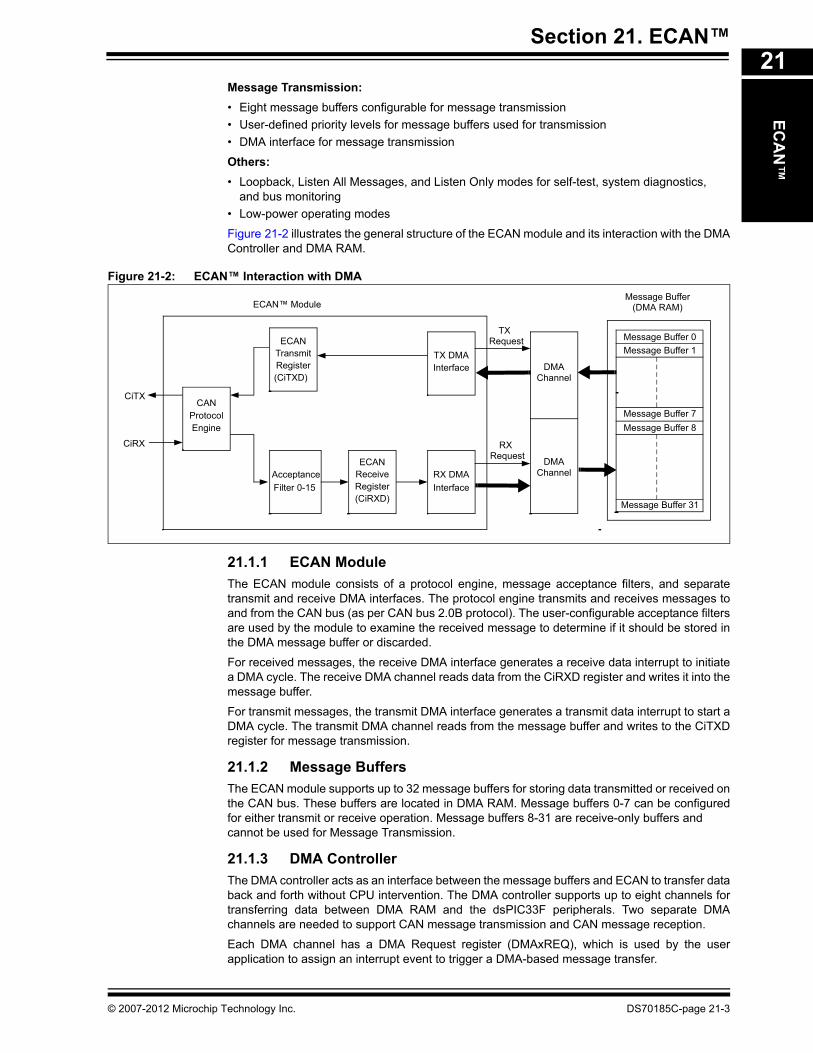
21.2 CAN MESSAGE FORMATSThe CAN bus protocol uses asynchronous communication. Information is passed from transmit-ters to receivers in data frames, which are composed of byte fields that define the contents of thedata frame, as shown in Figure 21-3.
Each frame begins with a Start-of-Frame (SOF) bit and terminates with an End-of-Frame (EOF)bit field. The Start-of-Frame is followed by Arbitration and Control fields, which identify the mes-sage type, format, length and priority. This information allows each node on the CAN bus torespond appropriately to the message. The Data field conveys the message content and is vari-able length, ranging from 0 to 8 bytes. Error protection is provided by the Cyclic RedundancyCheck (CRC) and Acknowledgement (ACK) fields.
Figure 21-3: CAN Bus Message Frame
The CAN bus protocol supports five frame types:
• Data Frame – carries data from transmitter to the receivers• Remote Frame – transmitted by a node on the bus, to request transmission of a data
frame with the same identifier from another node• Error Frame – transmitted by any node when it detects an error• Overload Frame – provides an extra delay between successive Data or remote frames• Interframe Space – provides a separation between successive frames
The CAN 2.0B specification defines two additional data formats:
• Standard Data Frame – intended for standard messages that use 11 identifier bits• Extended Data Frame – intended for extended messages that use 29 identifier bits
There are three versions of CAN Bus specifications:
• 2.0A – considers 29-bit identifier as error• 2.0B Passive – ignores 29-bit identifier messages• 2.0B Active – handles both 11-bit and 29-bit identifier
The dsPIC33F ECAN module is compliant with the CAN 2.0B active specification, while providingenhanced message filtering capabilities.
Note: Refer to the Bosch CAN bus specification for detailed information on the CANprotocol.
SOF
ARBITRATION CONTROL DATAEOF
ACKCRC
DS70185C-page 21-4 © 2007-2012 Microchip Technology Inc.

Section 21. ECAN™EC
AN
™
21
21.2.1 Standard Data FrameThe standard data frame message begins with a Start-of-Frame bit followed by a 12-bit Arbitra-tion field, as shown in Figure 21-4. The Arbitration field contains an 11-bit identifier and theRemote Transmit Request (RTR) bit. The identifier defines the type of information contained inthe message and is used by each receiving node to determine if the message is of interest to it.The RTR bit distinguishes a data frame from a remote frame. For a standard data frame, the RTRbit is clear.Following the Arbitration field is a 6-bit Control field, which provides more information about thecontents of the message. The first bit in the Control field is an Identifier Extension (IDE) bit, whichdistinguishes the message as either a Standard or Extended data frame. A standard data frameis indicated by a dominant state (logic level ‘0’) during transmission of the IDE bit. The secondbit in the Control field is a Reserved (RB0) bit, which is in the dominant state (logic level ‘0’). Thelast 4 bits in the Control field represent the Data Length Code (DLC), which specifies the numberof data bytes present in the message.
The Data field follows the Control field. This field carries the message data – the actual payloadof the data frame. This field is variable length, ranging from 0 to 8 bytes. The number of bytes isuser-selectable.
The Data field is followed by the Cyclic Redundancy Check field, which is a 15-bit CRC sequencewith one delimiter bit.
The Acknowledgement (ACK) field is sent as a recessive bit (logic level ‘1’) and is overwritten asa dominant bit by any receiver that has received the data correctly. The message isacknowledged by the receiver irrespective of the result of the acceptance filter comparison.
The last field is the End-of-Frame (EOF) field, which consists of 7 recessive bits that indicate theend of the message.
Figure 21-4: Format of the Standard Data Frame
SID10 SID1
SOF
IDENTIFIER 11 Bits
RTR
IDE
RB0 DLC 4 Bits
DATA8 Bytes
CRC16 Bits
ACK2 Bits
EOF7 Bits
IFS3 Bits
SID0
9/19/2006 - 9/26/200611-bit Identifier
Interframe Space
9/19/2006 - 9/26/2006 9/19/2006 - 9/26/2006Data 9/19/2006 - 9/26/20069/19/2006 - 9/26/2006
9 - 9/26/2006
Frame Interframe Space9/19/2006 - 9/26/2006
IDE is Dominant (Logical ‘0’)
RTR is Dominant (Logical ‘0’)
RB0 is Dominant (Logical ‘0’)
/19/ArbitrationField
ControlField Field
CRCField
ACKField
End-of-
© 2007-2012 Microchip Technology Inc. DS70185C-page 21-5

dsPIC33F/PIC24H Family Reference Manual
21.2.2 Extended Data FrameThe extended data frame begins with an SOF bit followed by a 31-bit Arbitration field, as shownin Figure 21-5. The Arbitration field for the extended data frame contains 29 identifier bits in twofields separated by a Substitute Remote Request (SRR) bit and an IDE bit. SRR = 1 for extendeddata frames. The IDE bit indicates the data frame type. For the extended data frame, IDE = 1.
The extended data frame Control field consists of 7 bits. The first bit is the RTR. For the extendeddata frame, RTR = 0. The next two bits, RB1 and RB0, are reserved bits that are in the dominantstate (logic level ‘0’). The last 4 bits in the Control field are the Data Length Code, which specifiesthe number of data bytes present in the message.
The remaining fields in an extended data frame are identical to a standard data frame.
Figure 21-5: Format of the Extended Data Frame
SID10 SID1
SOF
IDENTIFIER 11 Bits
SRR
IDE
RTR
DLC 4 Bits
CRC16 Bits
ACK2 Bits
EOF7 Bits
IFS3 Bits
SID0
Field
29-bit Identifier
9/19/2006 - 9/26/2006Control
9/19/2006 - 9/26/2006CRC
9/19/2006 - 9/26/2006
IDENTIFIER 18 Bits
EID17 EID1 EID0
RB1
RB0
IDE is Recessive (Logical ‘1’)
SRR is Recessive (Logical ‘1’)
RTR is Dominant (Logical ‘0’)
RB0 is Dominant (Logical ‘0’)
RB1 is Dominant (Logical ‘0’)
9/19/2006 - 9/26/2006ACK End-of-
Frame
9/19/2006 - 9/26/20069/19/2006 - 9/26/2006Data
DATA8 Bytes
ArbitrationField Field Field Field
DS70185C-page 21-6 © 2007-2012 Microchip Technology Inc.

Section 21. ECAN™EC
AN
™
21
21.2.3 Remote FrameA node expecting to receive data from another node can initiate transmission of the respectivedata by the source node by sending a remote frame. A remote frame can be in standard format(see Figure 21-6) or extended format (see Figure 21-7).A Remote frame is similar to a data frame, with the following exceptions:
• The RTR bit is recessive (RTR = 1)• There is no Data field• The value of the DLC bits is 0 ≤ DLC ≤ 8
Figure 21-6: Format of the Standard Remote Frame
Figure 21-7: Format of the Extended Remote Frame
SID10 SID1
SOF
IDENTIFIER11 Bits
RTR
IDE
DLC 4 Bits
CRC16 Bits
ACK 2 Bits
EOF7 Bits
IFS3 Bits
SID0
11-bit Identifier
RB0
IDE is Dominant (Logical ‘0’)RTR is Recessive (Logical ‘1’)RB0 is Dominant (Logical ‘0’)
Arbitration Field Control Field CRC Field ACK Field End-of-Frame
SID10 SID0
SOF
IDENTIFIER 11 Bits
SRR
IDE
RTR
DLC 4 Bits
CRC16 Bits
ACK2 Bits
EOF7 Bits
IFS3 Bits
SID1
Arbitration Field
29-bit Identifier
Control Field CRC Field
IDENTIFIER 18 Bits
EID17 EID1 EID0
RB1
RB0
IDE is Recessive (Logical ‘1’)SRR is Recessive (Logical ‘1’)RTR is Recessive (Logical ‘1’)RB0 is Dominant (Logical ‘0’)RB1 is Dominant (Logical ‘0’)
ACK FieldEnd-of- Frame
© 2007-2012 Microchip Technology Inc. DS70185C-page 21-7

dsPIC33F/PIC24H Family Reference Manual
21.2.4 Error FrameAn Error Frame is generated by any node that detects a bus error. An error frame consists of anError Flag field followed by an Error Delimiter field. The Error Delimiter consists of 8 recessivebits and allows the bus nodes to restart communications cleanly after an error has occurred.There are two types of Error Flag fields, depending on the error status of the node that detectsthe error:
• Error Active Flag – contains 6 consecutive dominant bits, which forces all other nodes on the network to generate Error Echo Flags, thereby resulting in a series of 6 to 12 dominant bits on the bus.
• Error Passive Flag – contains 6 consecutive recessive bits, with the result that unless the bus error is detected by the transmitting node, the transmission of an Error Passive flag will not affect the communications of any other node on the network.
21.2.5 Overload FrameAn Overload Frame can be generated by a node either when a dominant bit is detected duringInterframe Space or when a node is not yet ready to receive the next message (for example, if itis still reading the previous received message). An Overload Frame has the same format as anError Frame with an Active Error Flag, but can only be generated during Interframe Space. It con-sists of an Overload Flag field with 6 dominant bits followed by an Overload Delimiter field with8 recessive bits. A node can generate a maximum of two sequential Overload Frames to delaythe start of the next message.
21.2.6 Interframe SpaceInterframe Space separates successive frames being transmitted on the CAN bus. It consists ofat least 3 recessive bits, referred to as Intermission. The Interframe Space allows nodes time tointernally process the previously received message before the start of the next frame. If the trans-mitting node is in the Error Passive state, an additional 8 recessive bits are inserted in the Inter-frame Space before any other message is transmitted by the node. This period is called aSuspend Transmit field and allows time for other transmitting nodes to take control of the bus.
DS70185C-page 21-8 © 2007-2012 Microchip Technology Inc.

Section 21. ECAN™EC
AN
™
21
21.3 ECAN REGISTERSThe ECAN module has a large number of Special Function Registers (SFRs) that are used toconfigure message acceptance filters and message buffers. To enable effective use of data RAMspace, multiple sets of SFRs are mapped onto the same set of memory addresses. The SFR MapWindow Select (WIN) bit in ECAN Control Register 1 (CiCTRL1<0>) is used to selectively accessone of these sets of SFRs.
If CiCTRL1<WIN> = 1, the message acceptance filters, masks and filter buffer pointer registersare accessed by the user application.
If CiCTRL1<WIN> = 0, the buffer control and status registers and the transmit and receive dataregisters are accessed by the user application.
21.3.1 ECAN Baud Rate Control Registers• CiCFG1: ECAN™ Baud Rate Configuration Register 1
This register contains control bits to set the period of each time quantum, using the baud rateprescaler, and specifies synchronization jump width in terms of time quanta (seeRegister 21-1).
• CiCFG2: ECAN™ Baud Rate Configuration Register 2This register is used to program the number of time quanta in each CAN bit segment, includingthe propagation and phase segments 1 and 2 (see Register 21-2).
21.3.2 ECAN Message Filter Registers• CiFEN1: ECAN™ Acceptance Filter Enable Register
This register enables/disables acceptance filters 0-15 for message filtering (seeRegister 21-3).
• CiRXFnSID: ECAN™ Acceptance Filter Standard Identifier Register n (n = 0-15)These 16 registers specify the standard message identifier for acceptance filters 0-15. Theidentifier bits are selectively masked against the incoming message identifier to determineif the message should be accepted or rejected (see Register 21-4). These registers are onlyaccessible by the user application when the WIN bit is set (CiCTRL1<0> = 1 = use filterwindow).
• CiRXFnEID: ECAN™ Acceptance Filter Extended Identifier Register n (n = 0-15)These 16 registers specify the extended message identifier for acceptance filters 0-15. Theidentifier bits are selectively masked against the incoming message identifier to determineif the message should be accepted or rejected (see Register 21-5). These registers are onlyaccessible by the user application when the WIN bit is set (CiCTRL1<0> = 1).
• CiRXMnSID: ECAN™ Acceptance Filter Mask Standard Identifier Register n (n = 0-2)These three registers specify the standard identifier mask bits for Acceptance Masks 0, 1and 2. Any acceptance filter can optionally select one of these mask registers to selectivelycompare the identifier bits (see Register 21-6). These registers are only accessible by theuser application when the WIN bit is set (CiCTRL1<0> = 1).
• CiRXMnEID: ECAN™ Acceptance Filter Mask Extended Identifier Register n (n = 0-2)There are three pairs of registers that specify Acceptance Mask bits for Mask 0, 1 and 2. Anyacceptance filter can optionally select one of the mask registers to selectively compare theidentifier bits (see Register 21-7). These registers are only accessible by the userapplication when the WIN bit is set (CiCTRL1<0> = 1).
• CiFMSKSEL1: ECAN™ Filter 7-0 Mask Selection Register 1This register is used with CiFMSKSEL2 to select the Acceptance mask for acceptancefilter 0-7 (see Register 21-8).
Note: The ‘i’ shown in register identifiers refers to ECAN 1 or ECAN 2.
© 2007-2012 Microchip Technology Inc. DS70185C-page 21-9

dsPIC33F/PIC24H Family Reference Manual
• CiFMSKSEL2: ECAN™ Filter 15-8 Mask Selection Register 2This register is used with CiFMSKSEL1 to select the Acceptance mask for acceptancefilter 8-15 (see Register 21-9).
• CiBUFPNT1: ECAN™ Filter 0-3 Buffer Pointer Register 1This register is used to specify the message buffer to be used for storing messagesaccepted by acceptance filters 0-3 (see Register 21-10). This register is only accessible bythe user application when the WIN bit is set (CiCTRL1<0> = 1).
• CiBUFPNT2: ECAN™ Filter 4-7 Buffer Pointer Register 2This register is used to specify the message buffer to be used for storing messagesaccepted by acceptance filters 4-7 (see Register 21-11). This register is only accessible bythe user application when the WIN bit is set (CiCTRL1<0> = 1).
• CiBUFPNT3: ECAN™ Filter 8-11 Buffer Pointer Register 3This register is used to specify the message buffer to be used for storing messagesaccepted by acceptance filters 8-11 (see Register 21-12). This register is only accessible bythe user application when the WIN bit is set (CiCTRL1<0> = 1).
• CiBUFPNT4: ECAN™ Filter 12-15 Buffer Pointer Register 4This register is used to specify the message buffer to be used for storing messagesaccepted by acceptance filters 12-15 (see Register 21-13). This register is only accessibleby the user application when the WIN bit is set (CiCTRL1<0> = 1).
21.3.3 ECAN Message Buffer Status Registers• CiRXFUL1: ECAN™ Receive Buffer Full Register 1
Paired with CiRXFUL2, this register indicates buffer full status for Message buffers 0-31.When a received message is stored into a message buffer, the respective buffer full flag isset (see Register 21-14). This register is only accessible by the user application when theWIN bit is cleared (CiCTRL1<0> = 0 = use buffer window).
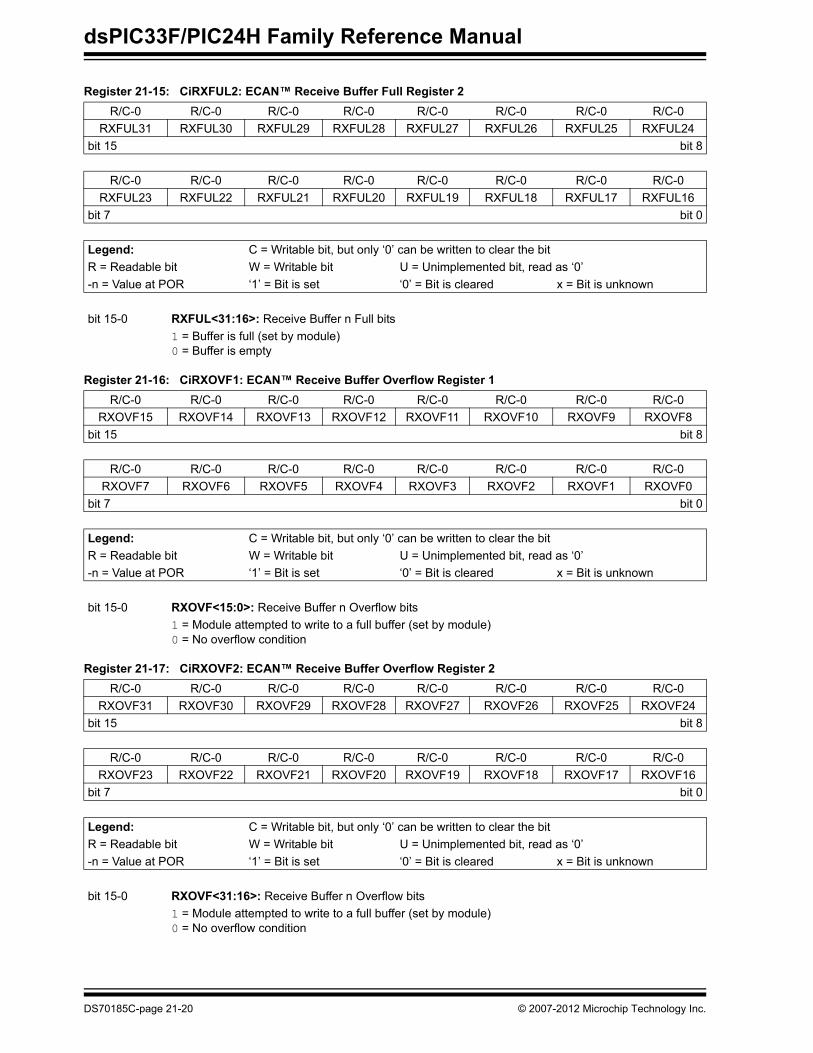
• CiRXFUL2: ECAN™ Receive Buffer Full Register 2Paired with CiRXFUL1, this register indicates buffer full status for Message buffers 0-31.When a received message is stored into a message buffer, the respective buffer full flag isset (see Register 21-15). This register is only accessible by the user application when theWIN bit is cleared (CiCTRL1<0> = 0).
• CiRXOVF1: ECAN™ Receive Buffer Overflow Register 1Paired with CiRXOVF2, this register indicates overflow status for Message buffers 0-31.When a received message is stored into a message buffer and the respective buffer full flagis set, the message is lost, and the respective buffer overflow flag is set (seeRegister 21-16). This register is only accessible by the user application when the WIN bit iscleared (CiCTRL1<0> = 0).
• CiRXOVF2: ECAN™ Receive Buffer Overflow Register 2Paired with CiRXOVF1, this register indicates overflow status for Message buffers 0-31.When a received message is stored into a message buffer and the respective buffer full flagis set, the message is lost, and the respective buffer overflow flag is set (seeRegister 21-17). This register is only accessible by the user application when the WIN bit iscleared (CiCTRL1<0> = 0).
DS70185C-page 21-10 © 2007-2012 Microchip Technology Inc.

Section 21. ECAN™EC
AN
™
21
21.3.4 ECAN FIFO Control/Status Registers• CiFCTRL: ECAN™ FIFO Control RegisterThis register controls operation of the receive buffer FIFO. It specifies the FIFO start addressand number of message buffers reserved for ECAN in DMA RAM (see Register 21-18). Thisregister is only accessible by the user application when the WIN bit is cleared (CiCTRL1<0> = 0).
• CiFIFO: ECAN™ FIFO Status RegisterThis register contains write and read pointers. The write pointer indicates which buffer con-tains the most-recently received data. The read pointer tells the user application which bufferto read next (see Register 21-19). This register is only accessible by the user applicationwhen the WIN bit is cleared (CiCTRL1<0> = 0).
21.3.5 ECAN Interrupt Control/Status Registers• CiINTF: ECAN™ Interrupt Flag Register
This register provides the status of various interrupt sources in the ECAN module (seeRegister 21-20). This register is only accessible by the user application when the WIN bit iscleared (CiCTRL1<0> = 0).
• CiINTE: ECAN™ Interrupt Enable RegisterThis register is used to selectively enable/disable 7 main sources of interrupt: transmit bufferinterrupt, receive buffer interrupt, receive buffer overflow interrupt, FIFO almost full interrupt,error interrupt, wake-up interrupt and invalid message received interrupt (seeRegister 21-21). This register is only accessible by the user application when the WIN bit iscleared (CiCTRL1<0> = 0).
• CiVEC: ECAN™ Interrupt Code RegisterThis register provides interrupt code bits that can be used with a jump table for efficienthandling of interrupts (see Register 21-22). This register is only accessible by the userapplication when the WIN bit is cleared (CiCTRL1<0> = 0).
21.3.6 ECAN Control and Error Counter Registers• CiCTRL1: ECAN™ Control Register 1
This register sets the ECAN module operation modes (see Register 21-23).
• CiCTRL2: ECAN™ Control Register 2This register contains the DeviceNet filtering control bits (see Register 21-24).
• CiTRmnCON: ECAN™ TX/RX Buffer m Control Register (m = 0,2,4,6; n = 1,3,5,7)These registers configure and control message buffers (see Register 21-25). This registeris only accessible by the user application when the WIN bit is cleared (CiCTRL1<0> = 0).
• CiEC: ECAN™ Transmit/Receive Error Count RegisterThis register counts transmit and receive errors. The user application can read this registerto determine the current number of transmit and receive errors (see Register 21-26).
• CiRXD: ECAN™ Receive Data RegisterThis register temporarily holds every received word. This is the register from which the DMAcontroller reads data into the DMA buffer.
• CiTXD: ECAN™ Transmit Data RegisterThis register temporarily holds every transmission. This is the register to which the DMAController writes data from the DMA buffer.
© 2007-2012 Microchip Technology Inc. DS70185C-page 21-11

dsPIC33F/PIC24H Family Reference Manual
Register 21-1: CiCFG1: ECAN™ Baud Rate Configuration Register 1U-0 U-0 U-0 U-0 U-0 U-0 U-0 U-0— — — — — — — —
bit 15 bit 8
R/W-0 R/W-0 R/W-0 R/W-0 R/W-0 R/W-0 R/W-0 R/W-0SJW<1:0> BRP<5:0>
bit 7 bit 0
Legend:R = Readable bit W = Writable bit U = Unimplemented bit, read as ‘0’-n = Value at POR ‘1’ = Bit is set ‘0’ = Bit is cleared x = Bit is unknown
bit 15-8 Unimplemented: Read as ‘0’bit 7-6 SJW<1:0>: Synchronization Jump Width bits
11 = Length is 4 x TQ 10 = Length is 3 x TQ 01 = Length is 2 x TQ 00 = Length is 1 x TQ
bit 5-0 BRP<5:0>: Baud Rate Prescaler bits11 1111 = TQ = 2 x 64 x 1/FCAN •••00 0010 = TQ = 2 x 3 x 1/FCAN00 0001 = TQ = 2 x 2 x 1/FCAN 00 0000 = TQ = 2 x 1 x 1/FCAN
DS70185C-page 21-12 © 2007-2012 Microchip Technology Inc.

Section 21. ECAN™EC
AN
™
21
Register 21-2: CiCFG2: ECAN™ Baud Rate Configuration Register 2U-0 R/W-x U-0 U-0 U-0 R/W-x R/W-x R/W-x— WAKFIL — — — SEG2PH<2:0>
bit 15 bit 8
R/W-x R/W-x R/W-x R/W-x R/W-x R/W-x R/W-x R/W-xSEG2PHTS SAM SEG1PH<2:0> PRSEG<2:0>
bit 7 bit 0
Legend:R = Readable bit W = Writable bit U = Unimplemented bit, read as ‘0’-n = Value at POR ‘1’ = Bit is set ‘0’ = Bit is cleared x = Bit is unknown
bit 15 Unimplemented: Read as ‘0’bit 14 WAKFIL: Select CAN Bus Line Filter for Wake-up bit
1 = Use CAN bus line filter for wake-up0 = CAN bus line filter is not used for wake-up
bit 13-11 Unimplemented: Read as ‘0’bit 10-8 SEG2PH<2:0>: Phase Segment 2 bits
111 = Length is 8 x TQ •••000 = Length is 1 x TQ
bit 7 SEG2PHTS: Phase Segment 2 Time Select bit1 = Freely programmable0 = Maximum of SEG1PH bits or Information Processing Time (IPT), whichever is greater
bit 6 SAM: Sample CAN Bus Line bit1 = Bus line is sampled three times at the sample point 0 = Bus line is sampled once at the sample point
bit 5-3 SEG1PH<2:0>: Phase Segment 1 bits111 = Length is 8 x TQ •••000 = Length is 1 x TQ
bit 2-0 PRSEG<2:0>: Propagation Time Segment bits111 = Length is 8 x TQ•••000 = Length is 1 x TQ
© 2007-2012 Microchip Technology Inc. DS70185C-page 21-13

dsPIC33F/PIC24H Family Reference Manual
Register 21-3: CiFEN1: ECAN™ Acceptance Filter Enable RegisterR/W-1 R/W-1 R/W-1 R/W-1 R/W-1 R/W-1 R/W-1 R/W-1
FLTEN15 FLTEN14 FLTEN13 FLTEN12 FLTEN11 FLTEN10 FLTEN9 FLTEN8bit 15 bit 8
R/W-1 R/W-1 R/W-1 R/W-1 R/W-1 R/W-1 R/W-1 R/W-1FLTEN7 FLTEN6 FLTEN5 FLTEN4 FLTEN3 FLTEN2 FLTEN1 FLTEN0
bit 7 bit 0
Legend: C = Writable bit, but only ‘0’ can be written to clear the bitR = Readable bit W = Writable bit U = Unimplemented bit, read as ‘0’-n = Value at POR ‘1’ = Bit is set ‘0’ = Bit is cleared x = Bit is unknown
bit 15-0 FLTENn: Enable Filter n bits1 = Enable filter n to accept messages 0 = Disable filter n
Register 21-4: CiRXFnSID: ECAN™ Acceptance Filter Standard Identifier Register n (n = 0-15)R/W-x R/W-x R/W-x R/W-x R/W-x R/W-x R/W-x R/W-xSID10 SID9 SID8 SID7 SID6 SID5 SID4 SID3
bit 15 bit 8
R/W-x R/W-x R/W-x U-0 R/W-x U-0 R/W-x R/W-xSID2 SID1 SID0 — EXIDE — EID17 EID16
bit 7 bit 0
Legend: C = Writable bit, but only ‘0’ can be written to clear the bitR = Readable bit W = Writable bit U = Unimplemented bit, read as ‘0’-n = Value at POR ‘1’ = Bit is set ‘0’ = Bit is cleared x = Bit is unknown
bit 15-5 SID<10:0>: Standard Identifier bits1 = Message address bit SIDx must be ‘1’ to match filter0 = Message address bit SIDx must be ‘0’ to match filter
bit 4 Unimplemented: Read as ‘0’bit 3 EXIDE: Extended Identifier Enable bit
If MIDE = 1:1 = Match only messages with extended identifier addresses0 = Match only messages with standard identifier addresses
If MIDE = 0:Ignore EXIDE bit.
bit 2 Unimplemented: Read as ‘0’bit 1-0 EID<17:16>: Extended Identifier bits
1 = Message address bit EIDx must be ‘1’ to match filter0 = Message address bit EIDx must be ‘0’ to match filter
Note: If no mask is applied to a filter, the filter will only accept Standard frames. The filter will not accept extendedframes even if the EXIDE bit is set to ‘1’.
DS70185C-page 21-14 © 2007-2012 Microchip Technology Inc.

Section 21. ECAN™EC
AN
™
21
Register 21-5: CiRXFnEID: ECAN™ Acceptance Filter Extended Identifier Register n (n = 0-15)R/W-x R/W-x R/W-x R/W-x R/W-x R/W-x R/W-x R/W-xEID15 EID14 EID13 EID12 EID11 EID10 EID9 EID8
bit 15 bit 8
R/W-x R/W-x R/W-x R/W-x R/W-x R/W-x R/W-x R/W-xEID7 EID6 EID5 EID4 EID3 EID2 EID1 EID0
bit 7 bit 0
Legend: C = Writable bit, but only ‘0’ can be written to clear the bitR = Readable bit W = Writable bit U = Unimplemented bit, read as ‘0’-n = Value at POR ‘1’ = Bit is set ‘0’ = Bit is cleared x = Bit is unknown
bit 15-0 EID<15:0>: Extended Identifier bits1 = Message address bit EIDx must be ‘1’ to match filter0 = Message address bit EIDx must be ‘0’ to match filter
Register 21-6: CiRXMnSID: ECAN™ Acceptance Filter Mask Standard Identifier Register n (n = 0-2)R/W-x R/W-x R/W-x R/W-x R/W-x R/W-x R/W-x R/W-xSID10 SID9 SID8 SID7 SID6 SID5 SID4 SID3
bit 15 bit 8
R/W-x R/W-x R/W-x U-0 R/W-x U-0 R/W-x R/W-xSID2 SID1 SID0 — MIDE — EID17 EID16
bit 7 bit 0
Legend: C = Writable bit, but only ‘0’ can be written to clear the bitR = Readable bit W = Writable bit U = Unimplemented bit, read as ‘0’-n = Value at POR ‘1’ = Bit is set ‘0’ = Bit is cleared x = Bit is unknown
bit 15-5 SID<10:0>: Standard Identifier bits1 = Include bit SIDx in filter comparison0 = Bit SIDx is “don’t care” in filter comparison
bit 4 Unimplemented: Read as ‘0’bit 3 MIDE: Identifier Receive Mode bit
1 = Match only message types (standard or extended address) that correspond to EXIDE bit in filter 0 = Match either standard or extended address message if filters match
(i.e., if (Filter SID) = (Message SID) or if (Filter SID/EID) = (Message SID/EID))bit 2 Unimplemented: Read as ‘0’bit 1-0 EID<17:16>: Extended Identifier bits
1 = Include bit EIDx in filter comparison0 = Bit EIDx is a “don’t care” in filter comparison
© 2007-2012 Microchip Technology Inc. DS70185C-page 21-15

dsPIC33F/PIC24H Family Reference Manual
Register 21-7: CiRXMnEID: ECAN™ Acceptance Filter Mask Extended Identifier Register n (n = 0-2)R/W-x R/W-x R/W-x R/W-x R/W-x R/W-x R/W-x R/W-xEID15 EID14 EID13 EID12 EID11 EID10 EID9 EID8
bit 15 bit 8
R/W-x R/W-x R/W-x R/W-x R/W-x R/W-x R/W-x R/W-xEID7 EID6 EID5 EID4 EID3 EID2 EID1 EID0
bit 7 bit 0
Legend: C = Writable bit, but only ‘0’ can be written to clear the bitR = Readable bit W = Writable bit U = Unimplemented bit, read as ‘0’-n = Value at POR ‘1’ = Bit is set ‘0’ = Bit is cleared x = Bit is unknown
bit 15-0 EID<15:0>: Extended Identifier bits1 = Include bit EIDx in filter comparison0 = Bit EIDx is “don’t care” in filter comparison
Register 21-8: CiFMSKSEL1: ECAN™ Filter 7-0 Mask Selection Register 1R/W-0 R/W-0 R/W-0 R/W-0 R/W-0 R/W-0 R/W-0 R/W-0
F7MSK<1:0> F6MSK<1:0> F5MSK<1:0> F4MSK<1:0>bit 15 bit 8
R/W-0 R/W-0 R/W-0 R/W-0 R/W-0 R/W-0 R/W-0 R/W-0F3MSK<1:0> F2MSK<1:0> F1MSK<1:0> F0MSK<1:0>
bit 7 bit 0
Legend: C = Writable bit, but only ‘0’ can be written to clear the bitR = Readable bit W = Writable bit U = Unimplemented bit, read as ‘0’-n = Value at POR ‘1’ = Bit is set ‘0’ = Bit is cleared x = Bit is unknown
bit 15-14 F7MSK<1:0>: Mask Source for Filter 7 bits11 = Reserved10 = Acceptance Mask 2 registers contain mask01 = Acceptance Mask 1 registers contain mask00 = Acceptance Mask 0 registers contain mask
bit 13-12 F6MSK<1:0>: Mask Source for Filter 6 bits (same values as bits 15-14)bit 11-10 F5MSK<1:0>: Mask Source for Filter 5 bits (same values as bits 15-14)bit 9-8 F4MSK<1:0>: Mask Source for Filter 4 bits (same values as bits 15-14)bit 7-6 F3MSK<1:0>: Mask Source for Filter 3 bits (same values as bits 15-14)bit 5-4 F2MSK<1:0>: Mask Source for Filter 2 bits (same values as bits 15-14)bit 3-2 F1MSK<1:0>: Mask Source for Filter 1 bits (same values as bits 15-14)bit 1-0 F0MSK<1:0>: Mask Source for Filter 0 bits (same values as bits 15-14)
DS70185C-page 21-16 © 2007-2012 Microchip Technology Inc.

Section 21. ECAN™EC
AN
™
21
Register 21-9: CiFMSKSEL2: ECAN™ Filter 15-8 Mask Selection Register 2R/W-0 R/W-0 R/W-0 R/W-0 R/W-0 R/W-0 R/W-0 R/W-0F15MSK<1:0> F14MSK<1:0> F13MSK<1:0> F12MSK<1:0>
bit 15 bit 8
R/W-0 R/W-0 R/W-0 R/W-0 R/W-0 R/W-0 R/W-0 R/W-0F11MSK<1:0> F10MSK<1:0> F9MSK<1:0> F8MSK<1:0>
bit 7 bit 0
Legend: C = Writable bit, but only ‘0’ can be written to clear the bitR = Readable bit W = Writable bit U = Unimplemented bit, read as ‘0’-n = Value at POR ‘1’ = Bit is set ‘0’ = Bit is cleared x = Bit is unknown
bit 15-14 F15MSK<1:0>: Mask Source for Filter 15 bits11 = Reserved10 = Acceptance Mask 2 registers contain mask01 = Acceptance Mask 1 registers contain mask00 = Acceptance Mask 0 registers contain mask
bit 13-12 F14MSK<1:0>: Mask Source for Filter 14 bits (same values as bits 15-14)bit 11-10 F13MSK<1:0>: Mask Source for Filter 13 bits (same values as bits 15-14)bit 9-8 F12MSK<1:0>: Mask Source for Filter 12 bits (same values as bits 15-14)bit 7-6 F11MSK<1:0>: Mask Source for Filter 11 bits (same values as bits 15-14)bit 5-4 F10MSK<1:0>: Mask Source for Filter 10 bits (same values as bits 15-14)bit 3-2 F9MSK<1:0>: Mask Source for Filter 9 bits (same values as bits 15-14)bit 1-0 F8MSK<1:0>: Mask Source for Filter 8 bits (same values as bits 15-14)
Register 21-10: CiBUFPNT1: ECAN™ Filter 0-3 Buffer Pointer Register 1R/W-0 R/W-0 R/W-0 R/W-0 R/W-0 R/W-0 R/W-0 R/W-0
F3BP<3:0> F2BP<3:0>bit 15 bit 8
R/W-0 R/W-0 R/W-0 R/W-0 R/W-0 R/W-0 R/W-0 R/W-0F1BP<3:0> F0BP<3:0>
bit 7 bit 0
Legend: C = Writable bit, but only ‘0’ can be written to clear the bitR = Readable bit W = Writable bit U = Unimplemented bit, read as ‘0’-n = Value at POR ‘1’ = Bit is set ‘0’ = Bit is cleared x = Bit is unknown
bit 15-12 F3BP<3:0>: RX Buffer mask for Filter 3 bits1111 = Filter hits received in RX FIFO buffer1110 = Filter hits received in RX Buffer 14•••0001 = Filter hits received in RX Buffer 10000 = Filter hits received in RX Buffer 0
bit 11-8 F2BP<3:0>: RX Buffer mask for Filter 2 bits (same values as bits 15-12)bit 7-4 F1BP<3:0>: RX Buffer mask for Filter 1 bits (same values as bits 15-12)bit 3-0 F0BP<3:0>: RX Buffer mask for Filter 0 bits (same values as bits 15-12)
© 2007-2012 Microchip Technology Inc. DS70185C-page 21-17

dsPIC33F/PIC24H Family Reference Manual
Register 21-11: CiBUFPNT2: ECAN™ Filter 4-7 Buffer Pointer Register 2R/W-0 R/W-0 R/W-0 R/W-0 R/W-0 R/W-0 R/W-0 R/W-0
F7BP<3:0> F6BP<3:0>bit 15 bit 8
R/W-0 R/W-0 R/W-0 R/W-0 R/W-0 R/W-0 R/W-0 R/W-0F5BP<3:0> F4BP<3:0>
bit 7 bit 0
Legend: C = Writable bit, but only ‘0’ can be written to clear the bitR = Readable bit W = Writable bit U = Unimplemented bit, read as ‘0’-n = Value at POR ‘1’ = Bit is set ‘0’ = Bit is cleared x = Bit is unknown
bit 15-12 F7BP<3:0>: RX Buffer mask for Filter 7 bits1111 = Filter hits received in RX FIFO buffer1110 = Filter hits received in RX Buffer 14•••0001 = Filter hits received in RX Buffer 10000 = Filter hits received in RX Buffer 0
bit 11-8 F6BP<3:0>: RX Buffer mask for Filter 6 bits (same values as bits 15-12)bit 7-4 F5BP<3:0>: RX Buffer mask for Filter 5 bits (same values as bits 15-12)bit 3-0 F4BP<3:0>: RX Buffer mask for Filter 4 bits (same values as bits 15-12)
Register 21-12: CiBUFPNT3: ECAN™ Filter 8-11 Buffer Pointer Register 3R/W-0 R/W-0 R/W-0 R/W-0 R/W-0 R/W-0 R/W-0 R/W-0
F11BP<3:0> F10BP<3:0>bit 15 bit 8
R/W-0 R/W-0 R/W-0 R/W-0 R/W-0 R/W-0 R/W-0 R/W-0F9BP<3:0> F8BP<3:0>
bit 7 bit 0
Legend: C = Writable bit, but only ‘0’ can be written to clear the bitR = Readable bit W = Writable bit U = Unimplemented bit, read as ‘0’-n = Value at POR ‘1’ = Bit is set ‘0’ = Bit is cleared x = Bit is unknown
bit 15-12 F11BP<3:0>: RX Buffer mask for Filter 111111 = Filter hits received in RX FIFO buffer1110 = Filter hits received in RX Buffer 14•••0001 = Filter hits received in RX Buffer 10000 = Filter hits received in RX Buffer 0
bit 11-8 F10BP<3:0>: RX Buffer mask for Filter 10 (same values as bit 15-12)bit 7-4 F9BP<3:0>: RX Buffer mask for Filter 9 (same values as bit 15-12)bit 3-0 F8BP<3:0>: RX Buffer mask for Filter 8 (same values as bit 15-12)
DS70185C-page 21-18 © 2007-2012 Microchip Technology Inc.

Section 21. ECAN™EC
AN
™
21
Register 21-13: CiBUFPNT4: ECAN™ Filter 12-15 Buffer Pointer Register 4R/W-0 R/W-0 R/W-0 R/W-0 R/W-0 R/W-0 R/W-0 R/W-0F15BP<3:0> F14BP<3:0>
bit 15 bit 8
R/W-0 R/W-0 R/W-0 R/W-0 R/W-0 R/W-0 R/W-0 R/W-0F13BP<3:0> F12BP<3:0>
bit 7 bit 0
Legend: C = Writable bit, but only ‘0’ can be written to clear the bitR = Readable bit W = Writable bit U = Unimplemented bit, read as ‘0’-n = Value at POR ‘1’ = Bit is set ‘0’ = Bit is cleared x = Bit is unknown
bit 15-12 F15BP<3:0>: RX Buffer mask for Filter 15 bits1111 = Filter hits received in RX FIFO Buffer1110 = Filter hits received in RX Buffer 14•••0001 = Filter hits received in RX Buffer 10000 = Filter hits received in RX Buffer 0
bit 11-8 F14BP<3:0>: RX Buffer mask for Filter 14 bits (same values as bits 15-12)bit 7-4 F13BP<3:0>: RX Buffer mask for Filter 13 bits (same values as bits 15-12)bit 3-0 F12BP<3:0>: RX Buffer mask for Filter 12 bits (same values as bits 15-12)
Register 21-14: CiRXFUL1: ECAN™ Receive Buffer Full Register 1R/C-0 R/C-0 R/C-0 R/C-0 R/C-0 R/C-0 R/C-0 R/C-0
RXFUL15 RXFUL14 RXFUL13 RXFUL12 RXFUL11 RXFUL10 RXFUL9 RXFUL8bit 15 bit 8
R/C-0 R/C-0 R/C-0 R/C-0 R/C-0 R/C-0 R/C-0 R/C-0RXFUL7 RXFUL6 RXFUL5 RXFUL4 RXFUL3 RXFUL2 RXFUL1 RXFUL0
bit 7 bit 0
Legend: C = Writable bit, but only ‘0’ can be written to clear the bitR = Readable bit W = Writable bit U = Unimplemented bit, read as ‘0’-n = Value at POR ‘1’ = Bit is set ‘0’ = Bit is cleared x = Bit is unknown
bit 15-0 RXFUL<15:0>: Receive Buffer n Full bits1 = Buffer is full (set by module) 0 = Buffer is empty
© 2007-2012 Microchip Technology Inc. DS70185C-page 21-19
dsPIC33F/PIC24H Family Reference Manual
Register 21-15: CiRXFUL2: ECAN™ Receive Buffer Full Register 2R/C-0 R/C-0 R/C-0 R/C-0 R/C-0 R/C-0 R/C-0 R/C-0
RXFUL31 RXFUL30 RXFUL29 RXFUL28 RXFUL27 RXFUL26 RXFUL25 RXFUL24bit 15 bit 8
R/C-0 R/C-0 R/C-0 R/C-0 R/C-0 R/C-0 R/C-0 R/C-0RXFUL23 RXFUL22 RXFUL21 RXFUL20 RXFUL19 RXFUL18 RXFUL17 RXFUL16
bit 7 bit 0
Legend: C = Writable bit, but only ‘0’ can be written to clear the bitR = Readable bit W = Writable bit U = Unimplemented bit, read as ‘0’-n = Value at POR ‘1’ = Bit is set ‘0’ = Bit is cleared x = Bit is unknown
bit 15-0 RXFUL<31:16>: Receive Buffer n Full bits1 = Buffer is full (set by module) 0 = Buffer is empty
Register 21-16: CiRXOVF1: ECAN™ Receive Buffer Overflow Register 1R/C-0 R/C-0 R/C-0 R/C-0 R/C-0 R/C-0 R/C-0 R/C-0
RXOVF15 RXOVF14 RXOVF13 RXOVF12 RXOVF11 RXOVF10 RXOVF9 RXOVF8bit 15 bit 8
R/C-0 R/C-0 R/C-0 R/C-0 R/C-0 R/C-0 R/C-0 R/C-0RXOVF7 RXOVF6 RXOVF5 RXOVF4 RXOVF3 RXOVF2 RXOVF1 RXOVF0
bit 7 bit 0
Legend: C = Writable bit, but only ‘0’ can be written to clear the bitR = Readable bit W = Writable bit U = Unimplemented bit, read as ‘0’-n = Value at POR ‘1’ = Bit is set ‘0’ = Bit is cleared x = Bit is unknown
bit 15-0 RXOVF<15:0>: Receive Buffer n Overflow bits1 = Module attempted to write to a full buffer (set by module) 0 = No overflow condition
Register 21-17: CiRXOVF2: ECAN™ Receive Buffer Overflow Register 2R/C-0 R/C-0 R/C-0 R/C-0 R/C-0 R/C-0 R/C-0 R/C-0
RXOVF31 RXOVF30 RXOVF29 RXOVF28 RXOVF27 RXOVF26 RXOVF25 RXOVF24bit 15 bit 8
R/C-0 R/C-0 R/C-0 R/C-0 R/C-0 R/C-0 R/C-0 R/C-0RXOVF23 RXOVF22 RXOVF21 RXOVF20 RXOVF19 RXOVF18 RXOVF17 RXOVF16
bit 7 bit 0
Legend: C = Writable bit, but only ‘0’ can be written to clear the bitR = Readable bit W = Writable bit U = Unimplemented bit, read as ‘0’-n = Value at POR ‘1’ = Bit is set ‘0’ = Bit is cleared x = Bit is unknown
bit 15-0 RXOVF<31:16>: Receive Buffer n Overflow bits1 = Module attempted to write to a full buffer (set by module) 0 = No overflow condition
DS70185C-page 21-20 © 2007-2012 Microchip Technology Inc.

Section 21. ECAN™EC
AN
™
21
Register 21-18: CiFCTRL: ECAN™ FIFO Control RegisterR/W-0 R/W-0 R/W-0 U-0 U-0 U-0 U-0 U-0DMABS<2:0> — — — — —
bit 15 bit 8
U-0 U-0 U-0 R/W-0 R/W-0 R/W-0 R/W-0 R/W-0— — — FSA<4:0>
bit 7 bit 0
Legend: C = Writable bit, but only ‘0’ can be written to clear the bitR = Readable bit W = Writable bit U = Unimplemented bit, read as ‘0’-n = Value at POR ‘1’ = Bit is set ‘0’ = Bit is cleared x = Bit is unknown
bit 15-13 DMABS<2:0>: DMA Buffer Size bits 111 = Reserved110 = 32 buffers in DMA RAM101 = 24 buffers in DMA RAM100 = 16 buffers in DMA RAM011 = 12 buffers in DMA RAM010 = 8 buffers in DMA RAM001 = 6 buffers in DMA RAM000 = 4 buffers in DMA RAM
bit 12-5 Unimplemented: Read as ‘0’bit 4-0 FSA<4:0>: FIFO Start Area bits
11111 = Read buffer RB31 11110 = Read buffer RB30 •••00010 = TX/RX buffer TRB200001 = TX/RX buffer TRB100000 = TX/RX buffer TRB0
© 2007-2012 Microchip Technology Inc. DS70185C-page 21-21

dsPIC33F/PIC24H Family Reference Manual
Register 21-19: CiFIFO: ECAN™ FIFO Status RegisterU-0 U-0 R-0 R-0 R-0 R-0 R-0 R-0— — FBP<5:0>
bit 15 bit 8
U-0 U-0 R-0 R-0 R-0 R-0 R-0 R-0— — FNRB<5:0>
bit 7 bit 0
Legend: C = Writable bit, but only ‘0’ can be written to clear the bitR = Readable bit W = Writable bit U = Unimplemented bit, read as ‘0’-n = Value at POR ‘1’ = Bit is set ‘0’ = Bit is cleared x = Bit is unknown
bit 15-14 Unimplemented: Read as ‘0’bit 13-8 FBP<5:0>: FIFO Buffer Pointer bits
011111 = RB31 buffer011110 = RB30 buffer•••000001 = TRB1 buffer000000 = TRB0 buffer
bit 7-6 Unimplemented: Read as ‘0’bit 5-0 FNRB<5:0>: FIFO Next Read Buffer Pointer bits
011111 = RB31 buffer011110 = RB30 buffer•••000001 = TRB1 buffer000000 = TRB0 buffer
DS70185C-page 21-22 © 2007-2012 Microchip Technology Inc.

Section 21. ECAN™EC
AN
™
21
Register 21-20: CiINTF: ECAN™ Interrupt Flag RegisterU-0 U-0 R-0 R-0 R-0 R-0 R-0 R-0— — TXBO TXBP RXBP TXWAR RXWAR EWARN
bit 15 bit 8
R/C-0 R/C-0 R/C-0 U-0 R/C-0 R/C-0 R/C-0 R/C-0IVRIF WAKIF ERRIF — FIFOIF RBOVIF RBIF TBIF
bit 7 bit 0
Legend: C = Writable bit, but only ‘0’ can be written to clear the bitR = Readable bit W = Writable bit U = Unimplemented bit, read as ‘0’-n = Value at POR ‘1’ = Bit is set ‘0’ = Bit is cleared x = Bit is unknown
bit 15-14 Unimplemented: Read as ‘0’bit 13 TXBO: Transmitter in Error State Bus Off bit
1 = Transmitter is in Bus Off state0 = Transmitter is not in Bus Off state
bit 12 TXBP: Transmitter in Error State Bus Passive bit1 = Transmitter is in Bus Passive state0 = Transmitter is not in Bus Passive state
bit 11 RXBP: Receiver in Error Bus Passive bit1 = Receiver is in Bus Passive state0 = Receiver is not in Bus Passive state
bit 10 TXWAR: Transmitter in Error State Warning bit1 = Transmitter is in Error Warning state0 = Transmitter is not in Error Warning state
bit 9 RXWAR: Receiver in Error State Warning bit1 = Receiver is in Error Warning state0 = Receiver is not in Error Warning state
bit 8 EWARN: Transmitter or Receiver in Error State Warning bit1 = Transmitter or receiver is in Error Warning state0 = Transmitter or receiver is not in Error Warning state
bit 7 IVRIF: Invalid Message Interrupt Flag bit1 = Interrupt request has occurred0 = Interrupt request has not occurred
bit 6 WAKIF: Bus Wake-up Activity Interrupt Flag bit1 = Interrupt request has occurred0 = Interrupt request has not occurred
bit 5 ERRIF: Error Interrupt Flag bit (multiple sources in CiINTF<13:8> register)1 = Interrupt request has occurred0 = Interrupt request has not occurred
bit 4 Unimplemented: Read as ‘0’bit 3 FIFOIF: FIFO Almost Full Interrupt Flag bit
1 = Interrupt request has occurred0 = Interrupt request has not occurred
bit 2 RBOVIF: RX Buffer Overflow Interrupt Flag bit1 = Interrupt request has occurred0 = Interrupt request has not occurred
bit 1 RBIF: RX Buffer Interrupt Flag bit1 = Interrupt request has occurred0 = Interrupt request has not occurred
bit 0 TBIF: TX Buffer Interrupt Flag bit1 = Interrupt request has occurred0 = Interrupt request has not occurred
© 2007-2012 Microchip Technology Inc. DS70185C-page 21-23

dsPIC33F/PIC24H Family Reference Manual
Register 21-21: CiINTE: ECAN™ Interrupt Enable RegisterU-0 U-0 U-0 U-0 U-0 U-0 U-0 U-0— — — — — — — —
bit 15 bit 8
R/W-0 R/W-0 R/W-0 U-0 R/W-0 R/W-0 R/W-0 R/W-0IVRIE WAKIE ERRIE — FIFOIE RBOVIE RBIE TBIE
bit 7 bit 0
Legend: C = Writable bit, but only ‘0’ can be written to clear the bitR = Readable bit W = Writable bit U = Unimplemented bit, read as ‘0’-n = Value at POR ‘1’ = Bit is set ‘0’ = Bit is cleared x = Bit is unknown
bit 15-8 Unimplemented: Read as ‘0’bit 7 IVRIE: Invalid Message Interrupt Enable bit
1 = Interrupt request enabled0 = Interrupt request not enabled
bit 6 WAKIE: Bus Wake-up Activity Interrupt Flag bit1 = Interrupt request enabled0 = Interrupt request not enabled
bit 5 ERRIE: Error Interrupt Enable bit1 = Interrupt request enabled0 = Interrupt request not enabled
bit 4 Unimplemented: Read as ‘0’bit 3 FIFOIE: FIFO Almost Full Interrupt Enable bit
1 = Interrupt request enabled0 = Interrupt request not enabled
bit 2 RBOVIE: RX Buffer Overflow Interrupt Enable bit1 = Interrupt request enabled0 = Interrupt request not enabled
bit 1 RBIE: RX Buffer Interrupt Enable bit1 = Interrupt request enabled0 = Interrupt request not enabled
bit 0 TBIE: TX Buffer Interrupt Enable bit1 = Interrupt request enabled0 = Interrupt request not enabled
DS70185C-page 21-24 © 2007-2012 Microchip Technology Inc.

Section 21. ECAN™EC
AN
™
21
Register 21-22: CiVEC: ECAN™ Interrupt Code RegisterU-0 U-0 U-0 R-0 R-0 R-0 R-0 R-0— — — FILHIT<4:0>
bit 15 bit 8
U-0 R-1 R-0 R-0 R-0 R-0 R-0 R-0— ICODE<6:0>
bit 7 bit 0
Legend: C = Writable bit, but only ‘0’ can be written to clear the bitR = Readable bit W = Writable bit U = Unimplemented bit, read as ‘0’-n = Value at POR ‘1’ = Bit is set ‘0’ = Bit is cleared x = Bit is unknown
bit 15-13 Unimplemented: Read as ‘0’bit 12-8 FILHIT<4:0>: Filter Hit Number bits
10000-11111 = Reserved01111 = Filter 15•••00001 = Filter 100000 = Filter 0
bit 7 Unimplemented: Read as ‘0’bit 6-0 ICODE<6:0>: Interrupt Flag Code bits
1000101-1111111 = Reserved1000100 = FIFO almost full interrupt1000011 = Receiver overflow interrupt1000010 = Wake-up interrupt1000001 = Error interrupt1000000 = No interrupt•••0100000-0111111 = Reserved0011111 = RB31 buffer interrupt 0011110 = RB30 buffer interrupt •••0001001 = RB9 buffer interrupt 0001000 = RB8 buffer interrupt 0000111 = TRB7 buffer interrupt0000110 = TRB6 buffer interrupt0000101 = TRB5 buffer interrupt0000100 = TRB4 buffer interrupt0000011 = TRB3 buffer interrupt0000010 = TRB2 buffer interrupt0000001 = TRB1 buffer interrupt0000000 = TRB0 buffer interrupt
© 2007-2012 Microchip Technology Inc. DS70185C-page 21-25

dsPIC33F/PIC24H Family Reference Manual
Register 21-23: CiCTRL1: ECAN™ Control Register 1U-0 U-0 R/W-0 R/W-0 r-0 R/W-1 R/W-0 R/W-0— — CSIDL ABAT — REQOP<2:0>
bit 15 bit 8
R-1 R-0 R-0 U-0 R/W-0 U-0 U-0 R/W-0OPMODE<2:0> — CANCAP — — WIN
bit 7 bit 0
Legend: C = Writable bit, but only ‘0’ can be written to clear the bit r = Bit is reservedR = Readable bit W = Writable bit U = Unimplemented bit, read as ‘0’-n = Value at POR ‘1’ = Bit is set ‘0’ = Bit is cleared x = Bit is unknown
bit 15-14 Unimplemented: Read as ‘0’bit 13 CSIDL: Stop in Idle Mode bit
1 = Discontinue module operation when device enters Idle mode0 = Continue module operation in Idle mode
bit 12 ABAT: Abort All Pending Transmissions bit1 = Signal all transmit buffers to abort transmission0 = Module will clear this bit when all transmissions are aborted
bit 11 Reserved: Do not usebit 10-8 REQOP<2:0>: Request Operation Mode bits
111 = Set Listen All Messages mode110 = Reserved101 = Reserved100 = Set Configuration mode011 = Set Listen-Only Mode010 = Set Loopback mode001 = Set Disable mode000 = Set Normal Operation mode
bit 7-5 OPMODE<2:0>: Operation Mode bits111 = Module is in Listen All Messages mode110 = Reserved101 = Reserved100 = Module is in Configuration mode011 = Module is in Listen-Only mode010 = Module is in Loopback mode001 = Module is in Disable mode000 = Module is in Normal Operation mode
bit 4 Unimplemented: Read as ‘0’bit 3 CANCAP: CAN Message Receive Timer Capture Event Enable bit
1 = Enable input capture based on CAN message receive 0 = Disable CAN capture
bit 2-1 Unimplemented: Read as ‘0’bit 0 WIN: SFR Map Window Select bit
1 = Use filter window 0 = Use buffer window
DS70185C-page 21-26 © 2007-2012 Microchip Technology Inc.

Section 21. ECAN™EC
AN
™
21
Register 21-24: CiCTRL2: ECAN™ Control Register 2U-0 U-0 U-0 U-0 U-0 U-0 U-0 U-0— — — — — — — —
bit 15 bit 8
U-0 U-0 U-0 R-0 R-0 R-0 R-0 R-0— — — DNCNT<4:0>
bit 7 bit 0
Legend: C = Writable bit, but only ‘0’ can be written to clear the bitR = Readable bit W = Writable bit U = Unimplemented bit, read as ‘0’-n = Value at POR ‘1’ = Bit is set ‘0’ = Bit is cleared x = Bit is unknown
bit 15-5 Unimplemented: Read as ‘0’bit 4-0 DNCNT<4:0>: DeviceNet™ Filter Bit Number bits
10011-11111 = Invalid selection 10010 = Compare bits <7:0> of byte 0 and bits <7:0> of byte 1 and bits <7:6> of byte 2 with EID<17:0>10001 = Compare bits <7:0> of byte 0 and bits <7:0> of byte 1 and bit <7> of byte 2 with EID<17:1>10000 = Compare bits <7:0> of data byte 0 and bits <7:0> of data byte 1 with EID<17:2>01111 = Compare bits <7:0> of data byte 0 and bits <7:1> of data byte 1 with EID<17:3>01110 = Compare bits <7:0> of data byte 0 and bits <7:2> of data byte 1 with EID<17:4>01101 = Compare bits <7:0> of data byte 0 and bits <7:3> of data byte 1 with EID<17:5>01100 = Compare bits <7:0> of data byte 0 and bits <7:4> of data byte 1 with EID<17:6>01011 = Compare bits <7:0> of data byte 0 and bits <7:5> of data byte 1 with EID<17:7>01001 = Compare bits <7:0> of data byte 0 and bit <7> of data byte 1 with EID<17:9>01010 = Compare bits <7:0> of data byte 0 and bits <7:6> of data byte 1 with EID<17:8>01000 = Compare bits <7:0> of data byte 0 with EID<17:10>00111 = Compare bits <7:1> of data byte 0 with EID<17:11>00110 = Compare bits <7:2> of data byte 0 with EID<17:12>00101 = Compare bits <7:3> of data byte 0 with EID<17:13>00100 = Compare bits <7:4> of data byte 0 with EID<17:14>00011 = Compare bits <7:5> of data byte 0 with EID<17:15>00010 = Compare bits <7:6> of data byte 0 with EID<17:16>00001 = Compare bit 7 of data byte 0 with EID<17>00000 = Do not compare data bytes
© 2007-2012 Microchip Technology Inc. DS70185C-page 21-27

dsPIC33F/PIC24H Family Reference Manual
Register 21-25: CiTRmnCON: ECAN™ TX/RX Buffer m Control Register (m = 0,2,4,6; n = 1,3,5,7)R/W-0 R-0 R-0 R-0 R/W-0 R/W-0 R/W-0 R/W-0TXENn TXABTn TXLARBn TXERRn TXREQn RTRENn TXnPRI<1:0>
bit 15 bit 8
R/W-0 R-0 R-0 R-0 R/W-0 R/W-0 R/W-0 R/W-0TXENm TXABTm(1) TXLARBm(1) TXERRm(1) TXREQm RTRENm TXmPRI<1:0>
bit 7 bit 0
Legend: C = Writable bit, but only ‘0’ can be written to clear the bitR = Readable bit W = Writable bit U = Unimplemented bit, read as ‘0’-n = Value at POR ‘1’ = Bit is set ‘0’ = Bit is cleared x = Bit is unknown
bit 15-8 Refer to definition for bits 7-0, Controls Buffer nbit 7 TXENm: TX/RX Buffer Selection bit
1 = Buffer TRBn is a transmit buffer0 = Buffer TRBn is a receive buffer
bit 6 TXABTm: Message Aborted bit(1)
1 = Message was aborted0 = Message completed transmission successfully
bit 5 TXLARBm: Message Lost Arbitration bit(1)
1 = Message lost arbitration while being sent0 = Message did not lose arbitration while being sent
bit 4 TXERRm: Error Detected During Transmission bit(1)
1 = A bus error occurred while the message was being sent0 = A bus error did not occur while the message was being sent
bit 3 TXREQm: Message Send Request bit1 = Requests that a message be sent. The bit automatically clears when the message is successfully
sent. 0 = Clearing the bit to ‘0’ while set requests a message abort.
bit 2 RTRENm: Auto-Remote Transmit Enable bit 1 = When a remote transmit is received, TXREQ is set0 = When a remote transmit is received, TXREQ is unaffected
bit 1-0 TXmPRI<1:0>: Message Transmission Priority bits11 = Highest message priority10 = High intermediate message priority01 = Low intermediate message priority00 = Lowest message priority
Note 1: This bit is cleared when TXREQ is set.
DS70185C-page 21-28 © 2007-2012 Microchip Technology Inc.

Section 21. ECAN™EC
AN
™
21
Register 21-26: CiEC: ECAN™ Transmit/Receive Error Count RegisterR-0 R-0 R-0 R-0 R-0 R-0 R-0 R-0TERRCNT<7:0>
bit 15 bit 8
R-0 R-0 R-0 R-0 R-0 R-0 R-0 R-0RERRCNT<7:0>
bit 7 bit 0
Legend: C = Writable bit, but only ‘0’ can be written to clear the bitR = Readable bit W = Writable bit U = Unimplemented bit, read as ‘0’-n = Value at POR ‘1’ = Bit is set ‘0’ = Bit is cleared x = Bit is unknown
bit 15-8 TERRCNT<7:0>: Transmit Error Count bitsbit 7-0 RERRCNT<7:0>: Receive Error Count bits
Register 21-27: CiRXD: ECAN™ Receive Data RegisterR/W-0 R/W-0 R/W-0 R/W-0 R/W-0 R/W-0 R/W-0 R/W-0
Received Data Wordbit 15 bit 8
R/W-0 R/W-0 R/W-0 R/W-0 R/W-0 R/W-0 R/W-0 R/W-0Received Data Word
bit 7 bit 0
Legend: C = Writable bit, but only ‘0’ can be written to clear the bitR = Readable bit W = Writable bit U = Unimplemented bit, read as ‘0’-n = Value at POR ‘1’ = Bit is set ‘0’ = Bit is cleared x = Bit is unknown
bit 15-0 DATA<15:0>: Receive Data bits
Register 21-28: CiTXD: ECAN™ Transmit Data RegisterR/W-0 R/W-0 R/W-0 R/W-0 R/W-0 R/W-0 R/W-0 R/W-0
Transmit Data Wordbit 15 bit 8
R/W-0 R/W-0 R/W-0 R/W-0 R/W-0 R/W-0 R/W-0 R/W-0Transmit Data Word
bit 7 bit 0
Legend: C = Writable bit, but only ‘0’ can be written to clear the bitR = Readable bit W = Writable bit U = Unimplemented bit, read as ‘0’-n = Value at POR ‘1’ = Bit is set ‘0’ = Bit is cleared x = Bit is unknown
bit 15-0 DATA<15:0>: Transmit Data bits
© 2007-2012 Microchip Technology Inc. DS70185C-page 21-29

dsPIC33F/PIC24H Family Reference Manual
21.4 ECAN MESSAGE BUFFERSECAN message buffers are located in DMA RAM. They are not ECAN Special FunctionRegisters. The user application must directly write into the DMA RAM area that is configured forECAN message buffers. The location and size of the buffer area is defined by the userapplication.
This section provides information on how the message buffer words are organized fortransmission and reception. (Refer to 21.2 “CAN Message Formats” for message buffer layoutdetails and 21.8 “DMA Controller Configuration” for details on how to configure ECANmessage buffers in DMA RAM.)
Buffer 21-1: ECAN Message Buffer Word 0U-0 U-0 U-0 R/W-x R/W-x R/W-x R/W-x R/W-x— — — SID10 SID9 SID8 SID7 SID6
bit 15 bit 8
R/W-x R/W-x R/W-x R/W-x R/W-x R/W-x R/W-x R/W-xSID5 SID4 SID3 SID2 SID1 SID0 SRR IDE
bit 7 bit 0
Legend:R = Readable bit W = Writable bit U = Unimplemented bit, read as ‘0’-n = Value at POR ‘1’ = Bit is set ‘0’ = Bit is cleared x = Bit is unknown
bit 15-13 Unimplemented: Read as ‘0’bit 12-2 SID<10:0>: Standard Identifier bitsbit 1 SRR: Substitute Remote Request bit
When TXIDE = 0:1 = Message will request remote transmission0 = Normal messageWhen TXIDE = 1:The SRR bit must be set to ‘1’
bit 0 IDE: Extended Identifier bit1 = Message will transmit extended identifier 0 = Message will transmit standard identifier
Buffer 21-2: ECAN Message Buffer Word 1U-0 U-0 U-0 U-0 R/W-x R/W-x R/W-x R/W-x— — — — EID17 EID16 EID15 EID14
bit 15 bit 8
R/W-x R/W-x R/W-x R/W-x R/W-x R/W-x R/W-x R/W-xEID13 EID12 EID11 EID10 EID9 EID8 EID7 EID6
bit 7 bit 0
Legend:R = Readable bit W = Writable bit U = Unimplemented bit, read as ‘0’-n = Value at POR ‘1’ = Bit is set ‘0’ = Bit is cleared x = Bit is unknown
bit 15-12 Unimplemented: Read as ‘0’bit 11-0 EID<17:6>: Extended Identifier bits
DS70185C-page 21-30 © 2007-2012 Microchip Technology Inc.

Section 21. ECAN™EC
AN
™
21
(Buffer 21-3: ECAN™ Message Buffer Word 2R/W-x R/W-x R/W-x R/W-x R/W-x R/W-x R/W-x R/W-xEID5 EID4 EID3 EID2 EID1 EID0 RTR RB1
bit 15 bit 8
U-0 U-0 U-0 R/W-x R/W-x R/W-x R/W-x R/W-x— — — RB0 DLC3 DLC2 DLC1 DLC0
bit 7 bit 0
Legend:R = Readable bit W = Writable bit U = Unimplemented bit, read as ‘0’-n = Value at POR ‘1’ = Bit is set ‘0’ = Bit is cleared x = Bit is unknown
bit 15-10 EID<5:0>: Extended Identifier bitsbit 9 RTR: Remote Transmission Request bit
When TXIDE = 1:1 = Message will request remote transmission0 = Normal messageWhen TXIDE = 0:The RTR bit is ignored.
bit 8 RB1: Reserved Bit 1User must set this bit to ‘0’ per CAN protocol.
bit 7-5 Unimplemented: Read as ‘0’bit 4 RB0: Reserved Bit 0
User must set this bit to ‘0’ per CAN protocol.bit 3-0 DLC<3:0>: Data Length Code bits
Buffer 21-4: ECAN™ Message Buffer Word 3R/W-x R/W-x R/W-x R/W-x R/W-x R/W-x R/W-x R/W-x
Byte 1bit 15 bit 8
R/W-x R/W-x R/W-x R/W-x R/W-x R/W-x R/W-x R/W-xByte 0
bit 7 bit 0Legend:R = Readable bit W = Writable bit U = Unimplemented bit, read as ‘0’-n = Value at POR ‘1’ = Bit is set ‘0’ = Bit is cleared x = Bit is unknown
bit 15-8 ECAN Message byte 1bit 7-0 ECAN Message byte 0
© 2007-2012 Microchip Technology Inc. DS70185C-page 21-31

dsPIC33F/PIC24H Family Reference Manual
Buffer 21-5: ECAN™ Message Buffer Word 4R/W-x R/W-x R/W-x R/W-x R/W-x R/W-x R/W-x R/W-x
Byte 3bit 15 bit 8
R/W-x R/W-x R/W-x R/W-x R/W-x R/W-x R/W-x R/W-xByte 2
bit 7 bit 0Legend:R = Readable bit W = Writable bit U = Unimplemented bit, read as ‘0’-n = Value at POR ‘1’ = Bit is set ‘0’ = Bit is cleared x = Bit is unknown
bit 15-8 ECAN Message byte 3bit 7-0 ECAN Message byte 2
Buffer 21-6: ECAN™ Message Buffer Word 5R/W-x R/W-x R/W-x R/W-x R/W-x R/W-x R/W-x R/W-x
Byte 5bit 15 bit 8
R/W-x R/W-x R/W-x R/W-x R/W-x R/W-x R/W-x R/W-xByte 4
bit 7 bit 0Legend:R = Readable bit W = Writable bit U = Unimplemented bit, read as ‘0’-n = Value at POR ‘1’ = Bit is set ‘0’ = Bit is cleared x = Bit is unknown
bit 15-8 ECAN Message byte 5bit 7-0 ECAN Message byte 4
Buffer 21-7: ECAN™ Message Buffer Word 6R/W-x R/W-x R/W-x R/W-x R/W-x R/W-x R/W-x R/W-x
Byte 7bit 15 bit 8
R/W-x R/W-x R/W-x R/W-x R/W-x R/W-x R/W-x R/W-xByte 6
bit 7 bit 0Legend:R = Readable bit W = Writable bit U = Unimplemented bit, read as ‘0’-n = Value at POR ‘1’ = Bit is set ‘0’ = Bit is cleared x = Bit is unknown
bit 15-8 ECAN Message byte 7bit 7-0 ECAN Message byte 6
DS70185C-page 21-32 © 2007-2012 Microchip Technology Inc.

Section 21. ECAN™EC
AN
™
21
Buffer 21-8: ECAN™ Message Buffer Word 7U-0 U-0 U-0 R/W-x R/W-x R/W-x R/W-x R/W-x— — — FILHIT4 FILHIT3 FILHIT2 FILHIT1 FILHIT0
bit 15 bit 8
U-0 U-0 U-0 U-0 U-0 U-0 U-0 U-0— — — — — — — —
bit 7 bit 0
Legend:R = Readable bit W = Writable bit U = Unimplemented bit, read as ‘0’-n = Value at POR ‘1’ = Bit is set ‘0’ = Bit is cleared x = Bit is unknown
bit 15-13 Unimplemented: Read as ‘0’bit 12-8 FILHIT<4:0>: Filter Hit Code bits
Encodes number of filter that resulted in writing this buffer (only written by module for receive buffers,unused for transmit buffers).
bit 7-0 Unimplemented: Read as ‘0’
© 2007-2012 Microchip Technology Inc. DS70185C-page 21-33

dsPIC33F/PIC24H Family Reference Manual
21.5 ECAN OPERATING MODESThe ECAN module can operate in one of several modes selected by the user application. Thesemodes include:
• Configuration mode• Normal Operation mode• Listen-Only mode• Listen All Messages mode• Loopback mode• Disable mode
Operating modes are requested by the user application writing to the Request Operation mode(REQOP<2:0>) bits in ECAN Control Register 1 (CiCTRL1<10:8>). ECAN acknowledges entryinto the requested mode by the Operation Mode (OPMODE<2:0>) bits (CiCTRL1<7:5>). Modetransition is performed in synchronization with the CAN network. That is, the ECAN controllerwaits until it detects a bus idle sequence (11 recessive bits) before it changes mode.
21.5.1 Configuration ModeAfter hardware reset, the ECAN module is in the Configuration mode (OPMODE<2:0> = 100).The error counters are cleared, and all registers contain the Reset values. In order to modify theECAN bit time control registers (CiCFG1 and CiCFG2), the ECAN module must be inConfiguration mode.
21.5.2 Normal Operation ModeIn Normal Operation mode, the ECAN module can transmit and receive CAN messages. NormalOperation mode is requested after initialization by programming the REQOP<2:0> bits(CiCTRL1<10:8>) to ‘000’. When OPMODE<2:0> = 000, the module proceeds with normal operation.
21.5.3 Listen-Only Mode Listen-Only mode is used mainly for bus monitoring without actually participating in thetransmission process. The node in Listen-Only mode does not generate an acknowledge or errorframes – one of the other nodes must do it. The Listen-Only mode can be used for detecting thebaud rate on the CAN bus.
21.5.4 Listen All Messages ModeListen All Messages mode is used for system debugging. Basically, all messages are received,irrespective of their identifier, even when there is an error. If the Listen All Messages mode is acti-vated, transmission and reception operate the same as Normal Operation mode except that if amessage is received with an error, it is still transferred to message buffer.
21.5.5 Loopback ModeLoopback mode is used for self test to allow the ECAN module to receive its own message. Inthis mode, the ECAN transmit path is connected to the receive path internally. A “dummy”Acknowledge is provided, thereby eliminating the need for another node to provide theAcknowledge bit.
21.5.6 Disable ModeDisable mode is used to ensure a safe shutdown before putting the device in Sleep or Idle mode.That is, the ECAN controller waits until it detects a bus idle sequence (11 recessive bits) beforeit changes mode. When the module is in Disable mode, it stops its own clocks, having no effecton the CPU or other modules. The module wakes up when bus activity occurs or when the CPUsets OPMODE<2:0> to ‘000’.
The CiTX pin stays in the recessive state while the module is in Disable mode.
DS70185C-page 21-34 © 2007-2012 Microchip Technology Inc.

Section 21. ECAN™EC
AN
™
21
21.6 TRANSMITTING ECAN MESSAGESA node originating a message is a transmitter of that message. The node remains a transmitteruntil the bus becomes idle or the unit loses arbitration. Figure 21-8 illustrates a typical ECANtransmission process.
Message buffers 0-7 (located in DMA RAM) are configured to transmit or receive CAN messagesusing the TX/RX Buffer Selection (TXENn) bit in the corresponding ECAN TX/RX Buffer m Con-trol Register (CiTRmnCON<7>). If the TXENn bit is set, the message buffer is configured fortransmission. See 21.2 “CAN Message Formats” for the layout of standard and extendedframes in the message buffer and the states of IDE, SRR, RTR, RB0 and RB1 bits for StandardData, Extended Data, Standard Remote or Extended remote frames as per the CAN protocol.
21.6.1 Message Transmission FlowTo transmit a message over the CAN bus, the user application must perform these tasks:
• Configure a message buffer for transmission and assign a priority to the buffer• Write the CAN message in the message buffer located in DMA RAM• Set the transmit request bit for the buffer to initiate message transmission
Message transmission is initiated by setting the Message Send Request (TXREQm) bit in ECANTransmit/Receive Control Register (CiTRmnCON<3>). The TXREQm bit is cleared automaticallyafter the message is transmitted. Before the SOF is sent, all the buffers ready for transmissionare examined to determine which buffer has the highest priority. The transmit buffer with thehighest priority is sent first.
Each of the transmit message buffers can be assigned to any of the four user-application definedpriority levels using CiTRmnCON<TXnPRI> bits.
TXnPRI<1:0> Message Transmission Priority selections are:
• 11 = The transmit message has the highest priority• 10 = The transmit message has intermediate high priority• 01 = The transmit message has intermediate low priority• 00 = The transmit message has the lowest priority
There is a natural order of priority for message buffers that are assigned to the sameuser-application defined priority level. Message buffer 7 has the highest natural order of priority.User-application defined priority levels override the natural order of priority.
Figure 21-8: ECAN™ Transmission
Word 001
SRR IDE
Word 10
Word 21015
2
EID <5:0> DLC <3:0>4
12
9RTR RB1
SID <10:0>
EID <17:6>
8
FILHIT <4:0>8
Data byte 1
Data byte 3
Data byte 5
Data byte 7
Data byte 0
Data byte 2
Data byte 4
Data byte 6
Word 7
SID SRR EID RTR
SID RTR DLC
DLCMessage Buffer 0
Message Buffer 1
Message Buffer 2
Message Buffer 3 (TX)
Message Buffer 4
Message Buffer 5
Message Buffer 6
Message Buffer 7
Extended
Standard
ECAN™ Data Frames
Word 3
Word 4
Word 5
Word 6
RB0
DMA RAMTRANSMIT MESSAGE
TransmitPriority
Arbitration
1315
1215
1315
57
Identifier
Identifier
© 2007-2012 Microchip Technology Inc. DS70185C-page 21-35

dsPIC33F/PIC24H Family Reference Manual
Example 21-1 illustrates code to transmit a standard frame using message buffer 0.
Example 21-1: Code Example for Standard Data Frame Transmission /* Assign 32x8word Message Buffers for ECAN1 in DMA RAM */
unsigned int ecan1MsgBuf[32][8] __attribute__((space(dma)));DMA1STA = __builtin_dmaoffset(ecan1MsgBuf);
/* Configure Message Buffer 2 for Transmission and assign priority*/
C1TR01CONbits.TXEN0 = 0x1;C1TR01CONbits.TX0PRI = 0x3;
/* WRITE TO MESSAGE BUFFER 0 *//* CiTRBnSID = 0bxxx1 0010 0011 1100IDE = 0b0SRR = 0b0SID<10:0>= 0b100 1000 1111 */
ecan1MsgBuf[0][0] = 0x123C;
/* CiTRBnEID = 0bxxxx 0000 0000 0000EID<17:6> = 0b0000 0000 0000 */
ecan1MsgBuf[0][1] = 0x0000;
/* CiTRBnDLC = 0b0000 0000 xxx0 1111EID<17:6> = 0b000000RTR = 0b0RB1 = 0b0RB0 = 0b0DLC = 0b1000 */
ecan1MsgBuf[0][2] = 0x8;
/* WRITE MESSAGE DATA BYTES */
ecan1MsgBuf[0][3] = 0xabcd;ecan1MsgBuf[0][4] = 0xabcd;ecan1MsgBuf[0][5] = 0xabcd;ecan1MsgBuf[0][6] = 0xabcd;
/* REQUEST MESSAGE BUFFER 0 TRANSMISSION */
C1TR01CONbits.TXREQ0 = 0x1;
DS70185C-page 21-36 © 2007-2012 Microchip Technology Inc.

Section 21. ECAN™EC
AN
™
21
Example 21-2 illustrates code to transmit an extended frame using message buffer 2.Example 21-2: Code Example for Extended Data Frame Transmission
21.6.2 Aborting a Transmit MessageSetting the Abort All Pending Transmissions (ABAT) bit in ECAN Control Register 1(CiCTRL1<12>) requests an abort of all pending messages. To abort a specific message, theMessage Send Request (TXREQm) bit (CiTRmnCON<3>) associated with that message buffermust be cleared. In either case, the message is only aborted if the ECAN module has not startedtransmitting the message on the bus.
/* Assign 32x8word Message Buffers for ECAN1 in DMA RAM */unsigned int ecan1MsgBuf[32][8] __attribute__(space(dma));DMA1STA = __builtin_dmaoffset(ecan1MsgBuf);
/* Configure Message Buffer 2for Transmission and assign priority*/
C1TR23CONbits.TXEN2 = 0x1;C1TR23CONbits.TX2PRI = 0x2;
/* WRITE TO MESSAGE BUFFER 2 *//* CiTRBnSID = 0bxxx1 0010 0011 1101IDE = 0b1SRR = 0b0SID<10:0> : 0b100 1000 1111 */
ecan1MsgBuf[2][0] = 0x123D;
/* CiTRBnEID = 0bxxxx 1111 0000 0000EID<17:6> = 0b1111 0000 0000 */
ecan1MsgBuf[2][1] = 0x0F00;
/* CiTRBnDLC = 0b0000 1100 xxx0 1111EID<17:6> = 0b000011RTR = 0b0RB1 = 0b0RB0 = 0b0DLC = 0b1000 */
ecan1MsgBuf[2][2] = 0x0C08;
/* WRITE MESSAGE DATA BYTES */
ecan1MsgBuf[2][3] = 0xabcd;ecan1MsgBuf[2][4] = 0xabcd;ecan1MsgBuf[2][5] = 0xabcd;ecan1MsgBuf[2][6] = 0xabcd;
/* REQUEST MESSAGE BUFFER 2 TRANSMISSION */
C1TR23CONbits.TXREQ2 = 0x1;
© 2007-2012 Microchip Technology Inc. DS70185C-page 21-37

dsPIC33F/PIC24H Family Reference Manual
21.6.3 Remote Transmit Request/Response
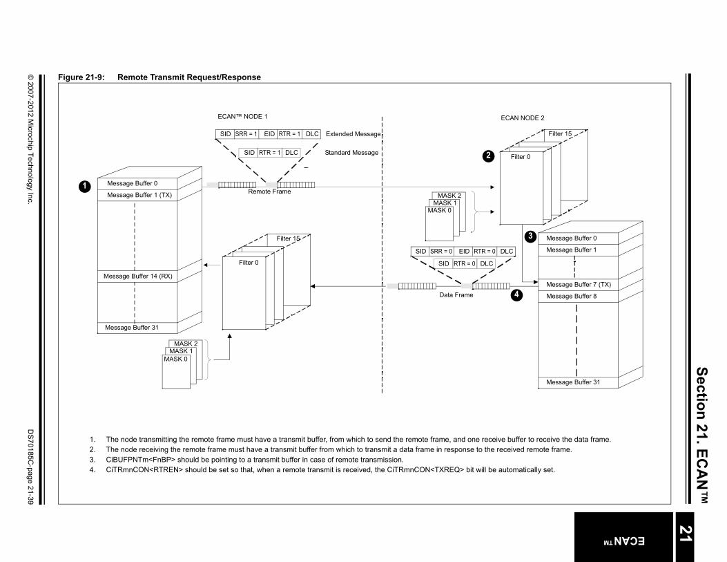
21.6.3.1 REMOTE TRANSMIT REQUEST
A node expecting to receive a data frame with a specific identifier value can initiate the transmis-sion of the respective data by another node by sending the remote frame. The remote frame canbe either in a Standard or Extended format.
A remote frame is similar to a data frame, with the following exceptions:
• The RTR bit is recessive (RTR = 1)• There is no data field• The value of the DLC bits is 0 ≤ DLC ≤ 8
To transmit a remote frame, the user application must perform these tasks:
• Configure the message buffer for transmission and assign a priority to the buffer• Write the remote frame in the appropriate message buffer. The transmitted identifier must
be identical to the identifier of the data frame to be received.• Set the transmit request bit for the buffer to initiate transmission of the remote frame
21.6.3.2 REMOTE TRANSMIT RESPONSE
The node that is acting as the source to respond to the remote frame request needs to configurean acceptance filter to match the identifier of the Remote Request Frame. Message buffers 0-7can respond to remote requests; therefore, the Acceptance Filter Buffer Pointer (FnBP) shouldpoint to one of the 8 message buffers. The TX/RX Buffer Selection (TXENn) and Auto-RemoteTransmit Enable (RTRENn) bits in the ECAN Transmit/Receive Control Register (CiTRmnCON)must be set to respond to the Remote Request Frame.
This is the only case where the Acceptance Filter Buffer Pointer (FnBP) points to a message buf-fer that is configured for transmission (TXENn = 1).
Figure 21-9 illustrates the remote frame handling process:
1. ECAN Node 1 sends a Remote Transmit Request (using message buffer 1).2. ECAN Node 2 receives the request and responds by sending the data frame (using
message buffer 7).3. The data frame is received by ECAN Node 1.4. The data frame is stored in message buffer 14 of ECAN Node 1.
Note: When configured for automatic response to remote requests (RTRENn = 1), theECAN module ignores the value of the DLC bit in the incoming RTR message. Ifthe application needs to transmit a data payload size specified by the DLC bits inthe received RTR message, it should not enable an automatic RTR response. Theuser application should process the RTR message like any other received mes-sage, check if the RTR bit is set, and then transmit a message whose payload sizeis equal to the DLC bits in the received RTR message.
DS70185C-page 21-38 © 2007-2012 Microchip Technology Inc.
© 2007-2012 M
icrochip Technology Inc.D
S70185C
-page 21-39
Section 21. ECA
N™
ECAN™
21
Fig
Filter 15
ilter 0
Message Buffer 0
Message Buffer 1
Message Buffer 7 (TX)
Message Buffer 8
Message Buffer 31
N NODE 2
4
3
ffer to receive the data frame.ved remote frame.
matically set.
ure 21-9: Remote Transmit Request/Response
MASK 2MASK 1
MASK 0
Filter 15
MASK 2MASK 1
MASK 0
Remote Frame
Data Frame
SID SRR = 0 EID RTR = 0 DLC
SID RTR = 0 DLC
SID SRR = 1 EID RTR = 1
SID RTR = 1 DLC
Extended Message
Standard Message
DLC
F
Filter 0
Message Buffer 0
Message Buffer 1 (TX)
Message Buffer 14 (RX)
Message Buffer 31
ECAN™ NODE 1 ECA
2
1
1. The node transmitting the remote frame must have a transmit buffer, from which to send the remote frame, and one receive bu2. The node receiving the remote frame must have a transmit buffer from which to transmit a data frame in response to the recei3. CiBUFPNTm<FnBP> should be pointing to a transmit buffer in case of remote transmission.4. CiTRmnCON<RTREN> should be set so that, when a remote transmit is received, the CiTRmnCON<TXREQ> bit will be auto

dsPIC33F/PIC24H Family Reference Manual
Example 21-3 illustrates the code required to transmit an extended remote frame using messagebuffer 2.
Example 21-3: Code Example for Transmitting Extended Remote Frame
/* Assign 32x8word Message Buffers for ECAN1 in DMA RAM */
unsigned int ecan1MsgBuf[32][8] __attribute__(space(dma));DMA1STA = __builtin_dmaoffset(ecan1MsgBuf);
/* Configure Message Buffer 0 for Transmission and assign priority*/
C1TR23CONbits.TXEN0 = 0x1;C1TR23CONbits.TX0PRI = 0x2;
/* WRITE TO MESSAGE BUFFER 0 *//* CiTRBnSID = 0bxxx1 0010 0011 1111IDE = 0b1SRR = 0b1SID<10:0> : 0b100 1000 1111 */
ecan1MsgBuf[2][0] = 0x123F;
/* CiTRBnEID = 0bxxxx 1111 0000 0000EID<17:6> = 0b1111 0000 0000 */
ecan1MsgBuf[2][1] = 0x0F00;
/* CiTRBnDLC = 0b0000 1110 xxx0 1111EID<17:6> = 0b000011RTR = 0b1RB1 = 0b0RB0 = 0b0DLC = 0b0 */
ecan1MsgBuf[2][2] = 0x0E00;
/* THERE ARE NO DATA BYTES FOR A REMOTE MESSAGE *//* REQUEST MESSAGE BUFFER 2 TRANSMISSION */
C1TR23CONbits.TXREQ2 = 0x1;
DS70185C-page 21-40 © 2007-2012 Microchip Technology Inc.

Section 21. ECAN™EC
AN
™
21
21.7 RECEIVING ECAN MESSAGESThe ECAN module can receive both standard and extended frames on the CAN bus node.Moreover, it has the additional capability of automatically transferring received messages touser-defined buffers in DMA RAM, thereby eliminating the need for the user application toexplicitly copy messages from hardware registers to user-defined buffers. The storage format ofeach message within the DMA buffer is identical to that of transmit buffers, with each message (including the associated status register) occupying 8 words in DMA RAM.
The two main stages that constitute the ECAN reception process are described in the followingsection. Figure 21-10 and Figure 21-13 are examples of a simplified reception process.
21.7.1 Message Reception and Acceptance FilteringAs shown in Figure 21-10, every incoming message on the bus is received into a MessageAssembly Buffer, and its identifier field is compared with a set of 16 user-defined acceptancefilters. Each received standard data frame contains an 11-bit Standard Identifier (SID), and eachextended data frame contains an 11-bit SID, and an 18-bit Extended Identifier (EID). If all bits inthe incoming identifier completely match the corresponding bits in any of the acceptance filters,the ECAN module generates a DMA transfer request to the DMA Controller so that the messagecan be received into the appropriate buffer in DMA RAM.
Figure 21-10: Message Reception and Acceptance Filtering
SID EID
Word 0Word 1Word 2Word 3Word 4Word 5Word 6Word 7
Filter 0Filter 1Filter 2Filter 3Filter 4Filter 5Filter 6Filter 7Filter 8Filter 9Filter 10Filter 11Filter 12Filter 13Filter 14Filter 15
IdentifierComparison
ECAN™ Data Frames
Filter Match (DMA Transfer Request)
MessageAssemblyBuffer
Acceptance Filters (0-15)
User-Defined
© 2007-2012 Microchip Technology Inc. DS70185C-page 21-41

dsPIC33F/PIC24H Family Reference Manual
21.7.1.1 ACCEPTANCE FILTERS
Figure 21-11 shows the incoming message identifier in comparison with filter/mask bits forstandard frames. Figure 21-12 shows the incoming message identifier in comparison withfilter/mask bits for extended frames.
Figure 21-11: Acceptance Filtering for a Standard Message
Figure 21-12: Acceptance Filtering for a Extended Message
Acceptance filters 0-15 can be individually enabled or disabled using the Enable Filter (FLTENn)bits in the ECAN Acceptance Filter Enable (CiFEN1<15:0>) register. The value of ‘n’ signifies theregister bit and corresponds to the index of the acceptance filter.
Acceptance filters 0-15 specify identifiers that must be contained in an incoming message for itscontents to be passed to a receive buffer. Each of these filters consists of two registers – one forStandard Identifiers and the other for Extended Identifiers. These registers are identified as:
• CiRXFnSID: ECAN Acceptance Filter n Standard Identifier register (where n = 0-15) • CiRXFnEID: ECAN Acceptance Filter n Extended Identifier register (where n = 0-15)
SID10 SID9
SOF
IDENTIFIER 11 Bits
RTR
IDE
DLC 4 Bits
CRC16 Bits
ACK2 Bits
EOF7 Bits
IFS3 Bits
SID1
11 bit Identifier
RB0DATA8 Bits
SID0
SID10 SID9 SID1 SID0 EXIDE CiRXFnSID
CiRXMnSIDSID10 SID9 SID1 SID0 MIDE
Accept/Reject Message
SID10 SID1
SOF
IDENTIFIER11 Bits
SRR
IDE
RTR
DLC4 Bits
CRC16 Bits
ACK EOF7 Bits
IFS3 Bits
SID0
-
29-bit Identifier
IDENTIFIER18 Bits
EID17 EID1 EID0
RB1
RB0
CiRXMnSID
CiRXFnSID
EID15 EID14 EID0
CiRXMnEID
SID10 SID0 EXIDE EID17 EID16
SID10 SID0 MIDE EID17 EID16 EID14 EID0EID15
CiRXFnEID
Accept/Reject Message
2 Bits
DS70185C-page 21-42 © 2007-2012 Microchip Technology Inc.

Section 21. ECAN™EC
AN
™
21
21.7.1.2 ACCEPTANCE FILTER MASKSAs shown in Figure 21-11 and Figure 21-12, an acceptance filter mask determines which bits inthe incoming message identifiers are examined with the acceptance filters.
Acceptance filters optionally select one of the acceptance filter masks using the Mask SourceSelect (FnMSK<1:0>) mask select bits in the CiFMSKSEL1 and CiFMSKSEL2 registers:
• CiFMSKSEL1<FnMSK>: Mask Selection for Filters 0-7• CiFMSKSEL2<FnMSK>: Mask Selection for Filters 8-15
The selection values for the FnMSK<1:0> bit are shown in Table 21-1.
Table 21-1: FnMSK<1:0> Selections and Values
Table 21-2 is a truth table that indicates how each bit in the identifier is compared to the masksand filters to determine if the message should be accepted or rejected. The mask bit essentiallydetermines which bits to apply the filter to. If any mask bit is set to a zero, that bit is automaticallyaccepted, regardless of the filter bit.
21.7.1.3 MESSAGE TYPE SELECTION
The Extended Identifier Enable (EXIDE) bit in the ECAN Acceptance Filter n Standard Identifier(CiRXFnSID<3>) register enables reception of either Standard Identifier or Extended Identifiermessages. The Identifier Receive Mode (MIDE) bit in the ECAN Acceptance Filter Mask n Stan-dard Identifier (CiRXMnSID<3>) register enables the CiRXFnSID<EXIDE> bit. If theCiRXMnSID<MIDE> bit is set, only the type of message selected by the CiRXFnSID<EXIDE> bitis accepted. If CiRXMnSID<MIDE> is clear, the CiRXFnSID<EXIDE> bit is ignored and allmessages that match the filter are accepted.
Table 21-3 shows the bit settings and resulting selection.
Table 21-3: EXIDE and MIDE Selections
Value Selection
00 Select acceptance filter mask 001 Select acceptance filter mask 110 Select acceptance filter mask 211 Reserved
Table 21-2: Acceptance Filter/Mask Truth Table
Mask (SIDn/EIDn) Filter (SIDn/EIDn) Message (SIDn/EIDn) Accept or Reject bit n
0 x x Accept1 0 0 Accept1 0 1 Reject1 1 0 Reject1 1 1 Accept
EXIDE MIDE Selection
0 1 Acceptance filter to check for standard identifier.1 1 Acceptance filter to check for extended identifier.x 0 Acceptance filter to check for standard/extended identifier.
© 2007-2012 Microchip Technology Inc. DS70185C-page 21-43

dsPIC33F/PIC24H Family Reference Manual
21.7.1.4 ACCEPTANCE FILTER CONFIGURATION
Example 21-4 illustrates the code to configure acceptance filter 0 to receive Standard Identifiermessages using the acceptance filter mask register to mask SID<2:0> bits.
Example 21-4: Code Example for Filtering Standard Data Frame
/* Enable Window to Access Acceptance Filter Registers */C1CTRL1bits.WIN=0x1;
/* Select Acceptance Filter Mask 0 for Acceptance Filter 0 */C1FMSKSEL1bits.F0MSK=0x0;
/* Configure Acceptance Filter Mask 0 register to mask SID<2:0>Mask Bits (11-bits) : 0b000 0000 0111 */C1RXM0SIDbits.SID = 0x0007;
/* Configure Acceptance Filter 0 to match standard identifierFilter Bits (11-bits): 0b011 1010 xxx */C1RXF0SIDbits.SID = 0x01D0;
/* Acceptance Filter 0 to check for Standard Identifier */C1RXM0SIDbits.MIDE = 0x1;C1RXF0SIDbits.EXIDE= 0x0;
/* Acceptance Filter 0 to use Message Buffer 10 to store message */C1BUFPNT1bits.F0BP = 0xA;
/* Filter 0 enabled for Identifier match with incoming message */C1FEN1bits.FLTEN0=0x1;
/* Clear Window Bit to Access ECAN Control Registers */C1CTRL1bits.WIN=0x0;
DS70185C-page 21-44 © 2007-2012 Microchip Technology Inc.

Section 21. ECAN™EC
AN
™
21
Example 21-5 illustrates the code to configure acceptance filter 2 to receive Extended Identifiermessages using the acceptance filter mask register to mask EID<5:0> bits.Example 21-5: Code Example for Filtering Extended Data Frame
/* Enable window to access acceptance filter registers */
C1CTRL1bits.WIN = 0x1;
/* Select Acceptance Filter Mask 1 for Acceptance Filter 2 */
C1FMSKSEL1bits.F2MSK=0x1;
/* Configure Acceptance Filter Mask 1 register to mask EID<5:0>Mask Bits (29-bits) : 0b0 0000 0000 0000 0000 0000 0011 1111SID<10:0> : 0b00000000000 ..SID<10:0> or EID<28:18>EID<17:16> : 0b00 ..EID<17:16>EID<15:0> : 0b0000000000111111 ..EID<15:0> */
C1RXM1SIDbits.SID = 0x0;C1RXM1SIDbits.EID = 0x0;C1RXM1EIDbits.EID = 0x3F;
/* Configure Acceptance Filter 2 to match extended identifierFilter Bits (29-bits) : 0b1 1110 0000 0011 1111 0101 10xx xxxxSID<10:0> : 0b11110000000 ..SID<10:0> or EID<28:18>EID<17:16> : 0b11 ..EID<17:16>EID<15:0> : 0b1111010110xxxxxx ..EID<15:0> */
C1RXF2SIDbits.SID = 0x780;C1RXF2SIDbits.EID = 0x3;C1RXM2EIDbits.EID = 0xF680;
/* Acceptance Filter 2 to check for Extended Identifier */
C1RXM1SIDbits.MIDE = 0x1;C1RXF2SIDbits.EXIDE= 0x1;
/* Acceptance Filter 2 to use Message Buffer 5 to store message */
C1BUFPNT1bits.F2BP = 0x6;
/* Enable Acceptance Filter 2 */
C1FEN1bits.FLTEN1=0x1;
© 2007-2012 Microchip Technology Inc. DS70185C-page 21-45

dsPIC33F/PIC24H Family Reference Manual
21.7.2 Buffer Selection and DMA TransferAs shown in Figure 21-13, if a filter match occurs, a DMA transfer request is generated by theECAN module to the DMA Controller to automatically copy the received message into the appro-priate message buffer in a user-defined DMA RAM area. The ECAN module supports up to 32message buffers. The user application can use DMA Buffer Size (DMABS<2:0>) bits in the ECANFIFO Control (CiFCTRL<15:13>) register to select either 4, 6, 8, 12, 16, 24 or 32 message buf-fers. The selection of the receive buffer index (and therefore the DMA RAM addresses in whicha message is written by the DMA Controller) is dependent on which filter matched the incomingidentifier, and is user-configurable. The DMA Controller moves the data into the appropriateaddresses in the DMA RAM area and generates a DMA interrupt after the user-specified numberof words are transferred. Please refer to 21.8 “DMA Controller Configuration” for more detailson DMA channel configuration for ECAN data transfers.
Figure 21-13: Buffer Selection and DMA Transfer
Word 0Word 1Word 2Word 3Word 4Word 5Word 6Word 7
Filter 0Filter 1Filter 2Filter 3Filter 4Filter 5Filter 6Filter 7Filter 8Filter 9Filter 10Filter 11Filter 12Filter 13Filter 14Filter 15
IdentifierComparison
Filter Match
MessageAssemblyBuffer
Acceptance Filters(0-15)
User-Defined
F0BP<3:0>F1BP<3:0>F2BP<3:0>F3BP<3:0>F4BP<3:0>F5BP<3:0>F6BP<3:0>F7BP<3:0>F8BP<3:0>F9BP<3:0>F10BP<3:0>F11BP<3:0>F12BP<3:0>F13BP<3:0>F14BP<3:0>F15BP<3:0>
F1BP<3:0> = 0111
Message Buffer 0Message Buffer 1
Message Buffer 7
Message Buffer 31
ECAN™ Buffers in DMA RAM
DMA Transfer
Start of ECAN Buffers
+
x16
Message stored here
Filter Buffer Pointers (0-15)
DS70185C-page 21-46 © 2007-2012 Microchip Technology Inc.

Section 21. ECAN™EC
AN
™
21
21.7.2.1 BUFFER SELECTIONThere are four Acceptance Filter Buffer Pointer registers that select which message buffer thereceived message is stored into for acceptance filters 0 to 15.
• CiBUFPNT1<FnBP>: Buffer pointer for acceptance filters 0-3• CiBUFPNT2<FnBP>: Buffer pointer for acceptance filters 4-7• CiBUFPNT3<FnBP>: Buffer pointer for acceptance filters 8-11• CiBUFPNT4<FnBP>: Buffer pointer for acceptance filters 12-15
When the incoming message identifier is matched by one of the acceptance filters, the internallogic looks up the buffer pointer (FnBP<3:0>) and uses that as an address for the correspondingmessage buffer. The address is provided to the DMA channel by the peripheral. Hence the DMAchannel must be configured in Peripheral Indirect mode.
The values for FnBP<3:0> are interpreted as follows:
21.7.2.2 RECEIVING MESSAGES INTO MESSAGE BUFFERS 0-7
Message buffers 0-7 can be configured to transmit or receive CAN messages using the TX/RXBuffer Selection (TXENm) bit in the ECAN TX/RX Buffer m Control Register (CiTRmnCON<7>).The Acceptance Filter Buffer Pointer (FnBP) selects one of the message buffers to store receivedmessage, provided it is configured as a receive buffer (TXENm = 0).
If a message buffer is set up as a transmitter with the CiTRmnCON<RTRENn> bit set, and anacceptance filter pointing to that message buffer detects a message, the message buffer willhandle the RTR rather than store the message. This is the only case where the Acceptance FilterBuffer Pointer (FnBP) points to a message buffer that is configured for transmission (TXENn = 1).
21.7.2.3 RECEIVING MESSAGES INTO MESSAGE BUFFERS 8-14
Message buffers 8-14 are receive buffers. The Acceptance Filter Buffer Pointer (FnBP)determines which message buffer to use.
21.7.2.4 RECEIVING MESSAGES INTO MESSAGE BUFFERS 15-31
Message buffers 15-31 are receive buffers and are only usable as FIFO buffers because theAcceptance Filter Buffer Pointer (FnBP<3:0>) bits can only directly address 16 entities. WhenFnBP<3:0> = 1111, the results of a hit on that filter will write to the next available buffer locationwithin the FIFO.
0000 Message is received in message buffer 00001 Message is received in message buffer 1•••1110 Message is received in message buffer 141111 Message is received in Receive FIFO Buffer
Note: Multi-message buffering can be implemented by a user application by configuringmultiple acceptance filters with the same value. In this case, a received messagemay match multiple filters, and the ECAN module will assign the message to thelowest-numbered matching filter pointing to an empty buffer.
Note: The user application should not set the Transmit Request (TXREQ) bit in theCiTRmnCON register when the buffer is configured for receive operation(TXEN = 0). This could result in unpredictable module behavior.
© 2007-2012 Microchip Technology Inc. DS70185C-page 21-47

dsPIC33F/PIC24H Family Reference Manual
21.7.2.5 RECEIVE BUFFER STATUS BITS
The receive buffers contain two status bits per message buffer, the Message Buffer Full Flag(RXFULn) and the Message Buffer Overflow Flag (RXOVFn). These status bits are grouped intoregisters for buffer full status and buffer overflow status.
• CiRXFUL1<RXFULn>: Receive buffer full status for message buffers 0-15• CiRXFUL2<RXFULn>: Receive buffer full status for message buffers 16-31• CiRXOVF1<RXOVFn>: Receive buffer overflow status for message buffers 0-15• CiRXOVF2<RXOVFn>: Receive buffer overflow status for message buffers 16-31
When a received message is stored into a message buffer, the respective Buffer Full Flag(RXFULn) is set in the Receive Buffer Full register, and a received buffer interrupt(CiINTF<RBIF>) is generated. If an incoming message caused a filter match, and the messagebuffer assigned to the matching filter is full (i.e., the RXFULn bit associated with that buffer isalready ‘1’), the corresponding RXOVFn bit (where ‘n’ is the number of the message bufferassociated with that buffer) is set and a received buffer overflow interrupt is generated(CiINTF<RBOVIF>). The message is lost.
21.7.3 FIFO Buffer OperationThe ECAN module supports up to 32 message buffers. The user application can employ the DMABuffer Size (DMABS<2:0>) bits in the ECAN FIFO Control (CiFCTRL) register to specify 4, 6, 8,12, 16, 24 or 32 message buffers. The FIFO Start Area (FSA<4:0>) bits (CiFCTRL<4:0>)areused to specify the start of the FIFO within the buffer area. The end of FIFO is based on the number of message buffers defined in the DMABS<2:0> bits.
The user application should not allocate a FIFO area that contains transmit buffers. Should thiscondition occur, the module will attempt to point to the transmit buffer, but when a message isreceived for that buffer, an overflow condition causes the message contents to be lost.
Figure 21-14 shows that one of the message acceptance filters is set to store a received messagein FIFO (FnBP = 1111). The start of FIFO is set to message buffer 5 (CiFCTRL<FSA> = 00101)and the end of FIFO is set to message buffer 11 (CiFCTRL<DMABS> = 011) by allocating 12message buffers.
Figure 21-14: Receiving Messages in FIFO
Note: If multiple filters match the identifier of the incoming message, and all the messagebuffers assigned to all the matching filters are full, the RXOVFn bit correspondingto the lowest numbered matching filter is set.
MASK 2MASK 1
MASK 0
Filter 15
Filter Masks Message Acceptance Filters
FIFO
FIFO Buffer 0
FIFO Buffer n
Filter 0
FIFO Start
FIFO End
FnBP
DMA RAM
Message Buffer 0Message Buffer 1
Message Buffer 31
FIFO Buffer 1
Message Buffer 11
Message Buffer 5
1. The Acceptance Filter Buffer Pointer ‘FnBP’ should be ‘111’ to Store Received Message in FIFO.2. The starting address of FIFO is specified by CiFCTRL<FSA>. In the example above, FSA <4:0> = ‘00101’.3. End address of FIFO is given by CiFCTRL<DMABS>. In the example above, DMABS <2:0> = ‘011’.
12
3
DS70185C-page 21-48 © 2007-2012 Microchip Technology Inc.

Section 21. ECAN™EC
AN
™
21
21.7.3.1 RECEIVING MESSAGES INTO FIFO AREAThe acceptance filter stores the received message in the FIFO area when FnBP<3:0> = 1111.It uses a simple buffer pointer, beginning with the start of the FIFO as defined above, andincrementing sequentially through the set of buffers within the FIFO area. When the end of thebuffer is reached, the counter wraps and points to the start of FIFO area.
The write pointer value is accessible and (only) readable by the application software in theCiFIFO<FBP> bits. When the message is stored in the buffer, the RXFUL bit associated with thebuffer is set, and the FIFO buffer counter increments.
If the FBP<5:0> value points to a buffer, and the RXFUL bit associated with that buffer is already‘1’ at the time of the filter hit and before writing of the message contents, the RXOVL bitassociated with that buffer is set and the message is lost. After the message is lost, the FBP<5:0>value increments normally.
If the FBP<5:0> value points to a transmit/receive buffer that is selected as a transmit buffer atthe time of the filter hit and before writing of the message contents, the RXOVL bit associatedwith that buffer is set and the message is lost. After the message is lost, the FBP<5:0> valueincrements normally.
The application software unloads the FIFO by reading the contents of a buffer. Once the bufferlocation is read, the application software clears the RXFUL bit corresponding to that buffer. Whenan RXFUL bit is cleared, the number of that corresponding buffer, plus one, is written to theCiFIFO <FNRB> bits by the module. Application software can (only) read this value, left shift itby 4 bits and use it as an address offset for the next buffer to be read. The application softwareshould read the buffers sequentially.
The module generates an interrupt condition if the FIFO is about to fill. This condition is computedmathematically, as shown in Equation 21-1.
Equation 21-1: FIFO Interrupt Calculation
The interrupt is generated as the RXFUL bit is set for the buffer just written and after the FBP bithas been updated. The computation uses the updated FBP value.
21.7.4 FIFO ExampleFigure 21-15 illustrates seven examples of FIFO operation. The cases illustrated assume thatStart of FIFO is set to message buffer 5 (CiFCTRL<FSA> = 101) and End of FIFO is set tomessage buffer 11 (CiFCTRL<DMABS> = 011).
• Case 1 is the initialized case of the FIFO before any messages are received. The FIFO Buffer Pointer points to message buffer 5 (FRB = 5), and the FIFO Next Read Buffer Pointer points to message buffer 6 (FNRB = 5).
• Case 2 shows the FIFO after one message is received and transferred to message buffer 5. The FIFO Buffer Pointer is incremented (FBP = 6), and the RXFUL status bit for message buffer 5 is set (RXFUL = 1).
• Case 3 shows the FIFO after the sixth received message. The FIFO Buffer Pointer points to the last location in the FIFO area (FBP = 5 + 6 = 11), and the FIFO Next Read Pointer points to start of FIFO (FNRB = 5). In this case, FIFO is almost full and generates a FIFO interrupt.
• Case 4 shows the FIFO after the application software reads the first received message. When the application software clears the RXFUL status bit for message buffer 5, the module writes the FIFO Next Read Buffer Pointer with MB5 plus 1 (FNRB = 5 + 1 = 6).
• Case 5 shows the FIFO after the seventh message is received and written to message buffer 11. The RXFUL status bit for message buffer 11 is set (RXFUL = 1). Instead of incrementing, the FIFO Buffer Pointer is reloaded with the FIFO Start address (FBP = FSA = 5). Note that FBP is now mathematically one less than FNRB, which is the condition that generates the FIFO interrupt at the time the RXFUL status bit is set for message buffer 11.
FNRB - FBP = 1
or
(FNRB = START) AND (FBP = END)
© 2007-2012 Microchip Technology Inc. DS70185C-page 21-49

dsPIC33F/PIC24H Family Reference Manual
• Case 6 shows the FIFO after the eighth message is received and written to message buffer 5. Now the FIFO is full. There is no interrupt signaled for this condition.
• Case 7 shows the FIFO after the ninth received message. Now the FIFO has overflowed. The module sets the RXOVL bit for the buffer intended for writing. The message is lost. The module generates a receive overflow interrupt.
Figure 21-15: Example of FIFO Operation
MB 11 – RXFUL = 0MB 10 – RXFUL = 0
MB 9 – RXFUL = 0MB 8 – RXFUL = 0
MB 7 – RXFUL = 0MB 6 – RXFUL = 0
MB 5 – RXFUL = 0
MB 11 – RXFUL = 0
MB 10 – RXFUL = 0MB 9 – RXFUL = 0MB 8 – RXFUL = 0MB 7 – RXFUL = 0
MB 6 – RXFUL = 0MB 5 – RXFUL = 1
MB 11 – RXFUL = 0
MB 10 – RXFUL = 1MB 9 – RXFUL = 1MB 8 – RXFUL = 1MB 7 – RXFUL = 1MB 6 – RXFUL = 1
MB 5 – RXFUL = 1
MB 11 – RXFUL = 0MB 10 – RXFUL = 1MB 9 – RXFUL = 1MB 8 – RXFUL = 1MB 7 – RXFUL = 1
MB 6 – RXFUL = 1MB 5 – RXFUL = 0
MB 11 – RXFUL = 1
MB 10 – RXFUL = 1MB 9 – RXFUL = 1MB 8 – RXFUL = 1MB 7 – RXFUL = 1MB 6 – RXFUL = 1 RXOVL = 1
MB 5 – RXFUL = 1
MB 11 – RXFUL = 1MB 10 – RXFUL = 1MB 9 – RXFUL = 1MB 8 – RXFUL = 1MB 7 – RXFUL = 1
MB 6 – RXFUL = 1MB 5 – RXFUL = 1
MB 11 – RXFUL = 1MB 10 – RXFUL = 1MB 9 – RXFUL = 1
MB 8 – RXFUL = 1MB 7 – RXFUL = 1MB 6 – RXFUL = 1
MB 5 – RXFUL = 0
Case 1: FIFO at Start
Case 5: FIFO 7th Write(About to Fill)
Case 6: FIFO 8th Write FIFO Full
FNRB = 6
FBP = 5
FNRB = 6, FBP = 6
Case 7: FIFO 9th WriteFIFO Overflow
FBP = 7FNRB = 6
FNRB = 6
FBP = 11
Case 4: FIFO 1st Read
FNRB = 5
FBP = 11
FBP = 6FNRB = 5
FNRB = 5, FBP = 5
Case 2: FIFO 1st Write
Case 3: FIFO 6th Write
(About to Fill)
Legend: Shaded message buffers indicate the presence of a received message ready to be read by the user application.MB n represents message buffers 5-11.Write signifies that a message is stored in the FIFO message buffer and the RXFUL flag associated with that buffer is set. Read signifies that the application software unloads the FIFO message buffer by reading the contents of that buffer. Once the buffer location is read, the application software clears the RXFUL bit corresponding to that buffer.
DS70185C-page 21-50 © 2007-2012 Microchip Technology Inc.

Section 21. ECAN™EC
AN
™
21
21.7.5 DeviceNet™ FilteringThe DeviceNet filtering feature is based on CAN 2.0A protocol in which up to 18 bits of the datafield can be compared with the EID of the message acceptance filter in addition to the SID.The DeviceNet feature is enabled or disabled by the DeviceNet Filter Bit Number (DNCNT<4:0>)control bits in ECAN Control Register 2 (CiCTRL2<4:0>). The value specified in the DNCNT fielddetermines the number of data bits to be used for comparison with the EID bits of the messageacceptance filter. If the CiCTRL2<DNCNT> bits are cleared, the DeviceNet feature is disabled.
For a message to be accepted, the 11-bit SID must match the SID<10:0> bits in the messageacceptance filter and the first ‘n’ data bits in the message should match the EID<17:0> bits in themessage acceptance filter. For example, as shown in Figure 21-16, the first 18 data bits of thereceived message are compared with the corresponding identifier bits (EID<17:0>) of themessage acceptance filter.
Figure 21-16: ECAN™ Operation with DeviceNet™ Filtering
Note: The DeviceNet filtering feature will only function when all of the following are true:
• The message IDE bit = 0, which means the message is a standard ID message• The EXIDE bit in the CiRXFn register = 0• The MIDE bit in the CiRXMn register = 1• The value of the DNCNT bits is non-zero
SID10 SID9
SOF
Identifier11 Bits
EOF7 bits 3 bits
SID0
Accept/Reject Message
IFSData Byte 0 Data Byte 1 Data Byte 2
7 6 5 4 3 2 1 0 7 6 5 4 3 2 1 0 7 6 5 4 3 2 1 0Data Byte 0 Data Byte 1 Data Byte 2Message SID<10:0>
SID10 SID9 SID0 EID17 EID16 EID10 EID9 EID8 EID2 EID1 EID0
Standard Message Data Frame
Message Acceptance FilterSID<10:0>
Message Acceptance FilterEID<0:17>
Note: The DeviceNet™ filtering configuration shown for the EID bits is DNCNT<4:0> = 10010
© 2007-2012 Microchip Technology Inc. DS70185C-page 21-51

dsPIC33F/PIC24H Family Reference Manual
21.7.5.1 FILTER COMPARISONS
Table 21-4 shows the filter comparisons configured by the CiCTRL2(DNCNT<4:0>) control bits.For example, if DNCNT<4:0> = 00011, only a message in which the 11-bit Standard Identifiermatches the SID acceptance filter (SID<10:0>) and bits 7, 6 and 5 of Data Byte 0 match theExtended Identifier filter (EID<0:2>) is accepted.
21.7.5.2 SPECIAL CASES
There may be special cases when the message contains fewer data bits than are called for bythe DeviceNet filter configuration.
• Case 1 – If DNCNT <4:0> is greater than 18, indicating that the user application selected a number of bits greater than the total number of EID bits, the filter comparison terminates with the 18th bit of the data (bit 6 of data byte 2). If the SID and all 18 data bits match, the message is accepted.
• Case 2 – If DNCNT<4:0> is greater than 16, and the received message Data Length Code (DLC) is 2 (indicating a payload of two data bytes), the filter comparison terminates with the 16th bit of data (bit 0 of data byte 1). If the SID and all 16 bits match, the message is accepted.
• Case 3 – If DNCNT<4:0> is greater than 8, and the received message has DLC = 1 (indi-cating a payload of one data byte), the filter comparison terminates with the 8th bit of data (bit 0 of data byte 0). If the SID and all 8 bits match, the message is accepted.
• Case 4 – If DNCNT<4:0> is greater than 0, and the received message has DLC = 0, indi-cating no data payload, the filter comparison terminates with the Standard Identifier. If the SID matches, the message is accepted.
Table 21-4: DeviceNet™ Filter Bit Configurations
DeviceNet™ Filter Configuration (DNCNT<4:0>)
Received Message Data Bits to be Compared (Byte<bits>)
EID Bits Used for Acceptance
Filter
00000 No comparison No comparison00001 Data Byte 0<7> EID<17>00010 Data Byte 0<7:6> EID<17:16>00011 Data Byte 0<7:5> EID<17:15>00100 Data Byte 0<7:4> EID<17:14>00101 Data Byte 0<7:3> EID<17:13>00110 Data Byte 0<7:2> EID<17:12>00111 Data Byte 0<7:1> EID<17:11>01000 Data Byte 0<7:0> EID<17:10>01001 Data Byte 0<7:0> and Data Byte 1<7> EID<17:9>01010 Data Byte 0<7:0> and Data Byte 1<7:6> EID<17:8>01011 Data Byte 0<7:0> and Data Byte 1<7:5> EID<17:7>01100 Data Byte 0<7:0> and Data Byte 1<7:4> EID<17:6>01101 Data Byte 0<7:0> and Data Byte 1<7:3> EID<17:5>01110 Data Byte 0<7:0> and Data Byte 1<7:2> EID<17:4>01111 Data Byte 0<7:0> and Data Byte 1<7:1> EID<17:3>10000 Data Byte 0<7:0> and Data Byte 1<7:0> EID<17:2>10001 Byte 0<7:0> and Byte 1<7:0> and Byte 2<7> EID<17:1>10010 Byte 0<7:0> and Byte 1<7:0> and Byte 2<7:6> EID<17:0>
10011 to 11111 Invalid Selection Invalid Selection
DS70185C-page 21-52 © 2007-2012 Microchip Technology Inc.

Section 21. ECAN™EC
AN
™
21
21.8 DMA CONTROLLER CONFIGURATIONThe ECAN module uses a portion of DMA RAM for message buffers to support both transmissionand reception of CAN messages. The number of message buffers to be used by the ECANmodule is specified by the DMA Buffer Size (DMABS<2:0>) bits in the ECAN FIFO Control(CiFCTRL<15:13>) register. The DMAxSTA register in the DMA controller defines the start of theCAN buffer area. The DMA controller moves data between ECAN and the DMA message bufferswithout CPU intervention.
The DMA controller provides eight channels for data transfer between DMA RAM the dsPIC33Fperipherals that are DMA ready. Two DMA channels are needed to support both CAN messagetransmission and reception. Each channel has a Request Register (DMAxREQ) to assign anevent based on which message transfer occurs, as shown in Table 21-5.
Table 21-5: DMA Channel Request
An example showing the use of DMA Channel 4 to access the ECAN buffers is illustrated inFigure 21-17.
Figure 21-17: ECAN™ Message Buffer Memory Usage
Event IRQ Number to Initialize DMAxREQ Register
ECAN1 Reception 34ECAN1 Transmission 70ECAN2 Reception 55ECAN2 Transmission 71
16 BitsMSb LSb
&_DMA_BASE
Message Buffer 0
Message Buffer 31
&_DMA_BASE + DMA4STA
Data Memory Map DMA RAM
SFR Space
X Data RAM
Y Data RAM
DMA RAM
X DataUnimplemented
Note: Refer to the specific device data sheet for information on the DMA base address.
© 2007-2012 Microchip Technology Inc. DS70185C-page 21-53

dsPIC33F/PIC24H Family Reference Manual
21.8.1 DMA Operation for Transmitting DataThe user application selects a message for transmission by setting the Message Send Request(TXREQ) bit in the ECAN TX/RX Buffer m Control (CiTRmnCON<3>) register. The ECAN con-troller uses DMA to read the message from the message buffer and transmit the message. TheECAN module generates a transmit data interrupt to start a DMA cycle. In response to the inter-rupt, the DMA channel that is configured for ECAN message transmission reads from the mes-sage buffer in DMA RAM and stores the message in the ECAN Transmit Data (CiTXD) register.Eight words are transferred for every message transmitted by the ECAN controller. 21.2 “CANMessage Formats” provides the detailed layout of the transmit message buffer. Sample codefor configuring the DMA channel for ECAN 1 transmission is shown in Example 21-6.
Example 21-6: DMA Channel 0 Configuration for ECAN1 Transmission
Note: Please refer to Section 22 “Direct Memory Access (DMA)” (DS70182) for moreinformation on how to configure the DMA Controller. Check for the most recentdocumentation on the Microchip web site at www.microchip.com.
/* Assign 32x8 Word Message Buffers for ECAN1 in DMA RAM */unsigned int ecan1MsgBuf[32][8] __atribute__((space(dma)));
/* Data Transfer Size: Word Transfer Mode */DMA0CONbits.SIZE = 0x0;
/* Data Transfer Direction: DMA RAM to Peripheral */DMA0CONbits.DIR = 0x1;
/* DMA Addressing Mode: Peripheral Indirect Addressing mode */DMA0CONbits.AMODE = 0x2;
/* Operating Mode: Continuous, Ping-Pong modes disabled */DMA0CONbits.MODE = 0x0;
/* Assign ECAN1 Transmit event for DMA Channel 0 */DMA0REQ = 70;
/* Set Number of DMA Transfer per ECAN message to 8 words */DMA0CNT = 7;
/* Peripheral Address: ECAN1 Transmit Register */DMA0PAD = &C1TXD;
/* Start Address Offset for ECAN1 Message Buffer 0x0000 */DMA0STA = __builtin_dmaoffset(ecan1MsgBuf);
/* Channel Enable: Enable DMA Channel 0 */DMA0CONbits.CHEN = 0x1;
/* Channel Interrupt Enable: Enable DMA Channel 0 Interrupt */IEC0bits DMA0IE = 1;
DS70185C-page 21-54 © 2007-2012 Microchip Technology Inc.

Section 21. ECAN™EC
AN
™
21
21.8.2 DMA Operation for Receiving DataWhen the ECAN controller completes a received message (8 words), the completed message istransferred to a message buffer in DMA RAM by the DMA. The ECAN module generates areceive data interrupt to start a DMA cycle. In response to this interrupt, the DMA channel that isconfigured for ECAN message reception reads from the ECAN Receive Data (CiRXD) registerand stores the message in the DMA RAM buffer. Eight words are transferred for every messagethat is received by the ECAN controller. The detailed layout of the received message is providedin 21.2 “CAN Message Formats”. Sample code for configuring the DMA channel for ECAN1reception is shown in Example 21-7.Example 21-7: DMA Channel 1 Configuration for ECAN1 Reception
Note: Please refer to Section 22 “Direct Memory Access (DMA)” (DS70182) for moreinformation on how to configure the DMA Controller. Check for the most recentdocumentation on the Microchip web site at www.microchip.com.
/* Data Transfer Size: Word Transfer Mode */DMA1CONbits.SIZE = 0x0;
/* Data Transfer Direction: Peripheral to DMA RAM */DMA1CONbits.DIR = 0x0;
/* DMA Addressing Mode: Peripheral Indirect Addressing mode */DMA1CONbits.AMODE = 0x2;
/* Operating Mode: Continuous, Ping-Pong modes disabled */DMA1CONbits.MODE = 0x0;
/* Assign ECAN1 Receive event for DMA Channel 0 */DMA1REQ = 34;
/* Set Number of DMA Transfer per ECAN message to 8 words */DMA1CNT = 7;
/* Peripheral Address: ECAN1 Receive Register */DMA1PAD = &C1RXD;
/* Start Address Offset for ECAN1 Message Buffer 0x0000 */DMA1STA = 0x0000;
/* Channel Enable: Enable DMA Channel 1 */DMA1CONbits.CHEN = 0x1;
/* Channel Interrupt Enable: Enable DMA Channel 1 Interrupt */IEC0bits.DMA1IE = 1;
© 2007-2012 Microchip Technology Inc. DS70185C-page 21-55

dsPIC33F/PIC24H Family Reference Manual
21.9 BIT TIMINGThe nominal bit rate is the number of bits per second transmitted on the CAN bus: Nominal BitTime = 1 ÷ Nominal Bit Rate.
There are four time segments in a bit time to compensate for any phase shifts due to oscillatordrifts or propagation delays. These time segments do not overlap each other and are representedin terms of Time Quantum (TQ). One TQ is a fixed unit of time derived from the oscillator clock.The total number of time quanta in a nominal bit time must be programmed between 8 and 25 TQ.
Figure 21-18 shows how the time quanta clock (FTQ) is obtained from the system clock and alsohow the different time segments are programmed.
Figure 21-18: ECAN™ Bit Timing
21.9.1 Bit SegmentsEach bit transmission time consists of four time segments:
• Synchronization Segment – This time segment synchronizes the different nodes con-nected on the CAN bus. A bit edge is expected to be within this segment. Based on CAN protocol, the Synchronization Segment is assumed to be one TQ.
• Propagation Segment – This time segment compensates for any time delay that may occur due to the bus line or due to the various transceivers connected on that bus.
• Phase Segment 1 – This time segment compensates for errors that may occur due to phase shift in the edges. The time segment may be lengthened during resynchronization to compensate for the phase shift.
• Phase Segment 2 – This time segment compensates for errors that may occur due to phase shift in the edges. The time segment may be shortened during resynchronization to compensate for the phase shift. The Phase Segment 2 time can be configured to be either programmable or specified by the Phase Segment 1 time.
CAN Nominal Bit Time
Time Quanta
Time Segments Propagation Segment Phase Segment 1 Phase Segment 2Sync Seg1TQ 1-8TQ 1-8TQ 1-8TQ
Sample Point
BAUD RATEPRESCALER
FCY 2
Prop Seg
Phase Seg1
Phase Seg2
Sync Seg
FTQ
Time Quanta
CiCFG1<BRP>
CiCFG2<PRSEG>
CiCFG2<SEG1PH>
CiCFG2<SEG2PH>
CiCFG1<SJW>
1-8TQ1:11:2
1:64
(TQ)
1-8TQ
1-8TQ
1TQ
8-25 TQ
DS70185C-page 21-56 © 2007-2012 Microchip Technology Inc.
Section 21. ECAN™EC
AN
™
21
21.9.2 Sample PointThe sample point is the point in a CAN bit time interval where the sample is taken and the busstate is read and interpreted. It is situated between Phase Segment 1 and Phase Segment 2.The CAN bus can be sampled once or three times at the sample point, as configured by theSample CAN bus Line (SAM) bit in ECAN Baud Rate Configuration Register (CiCFG2<6>).• If CiCFG2<SAM> = 1, the CAN bus is sampled three times at the sample point. The most common of the three samples determines the bit value.
• If CiCFG2<SAM> = 0, the CAN bus is sampled only once at the sample point.
21.9.3 SynchronizationTwo types of synchronization are used – Hard Synchronization and Resynchronization. A HardSynchronization occurs once at the start of a frame. Resynchronization occurs inside a frame.
• Hard synchronization takes place on the recessive-to-dominant transition of the start bit. The bit time is restarted from that edge.
• Resynchronization takes place when a bit edge does not occur within the Synchronization Segment in a message. One of the Phase Segments is shortened or lengthened by an amount that depends on the phase error in the signal. The maximum amount that can be used is determined by the Synchronization Jump Width parameter (CiCFG1<SJW>).
The length of Phase Segment 1 and Phase Segment 2 can be changed depending on oscillatortolerances of the transmitting and receiving node. Resynchronization compensates for anyphase shifts that may occur due to the different oscillators used by the transmitting and receivingnodes.
• Bit Lengthening – If the transmitting node in ECAN has a slower oscillator than the receiv-ing node, the next falling edge, and hence the sample point, can be delayed by lengthening Phase Segment 1 in the bit time.
• Bit Shortening – If the transmitting node in ECAN has a faster oscillator than the receiving node, then the next falling edge, and hence the sample point of the next bit, can be reduced by shortening the Phase Segment 2 in the bit time.
• Synchronization Jump Width (SJW) – The SJW <1:0> bits in ECAN Baud Rate Configuration Register (CiCFG1<7:6>) determine the synchronization jump width by limit-ing the amount of lengthening or shortening that can be applied to the Phase Segment 1 and Phase Segment 2 time intervals. This segment should not be longer than Phase Segment 2 time. The width can be 1-4 TQ.
© 2007-2012 Microchip Technology Inc. DS70185C-page 21-57

dsPIC33F/PIC24H Family Reference Manual
21.9.4 ECAN Bit Time Calculations The steps that need to be performed by the user application to configure the bit timing for theECAN module are described below, which include examples.
1. Calculate the Time Quantum Frequency (FTQ):a) Select the Baud Rate for the CAN Bus (FBAUD).b) Select the number of tIme quanta in a bit time, based on your system requirements.
The Time Quantum Frequency (FTQ) is given by Equation 21-2:
Equation 21-2: Time Quantum Frequency Calculation
2. Calculate the Baud Rate Prescaler (CiCFG1<BRP>). The baud rate prescaler is given byEquation 21-3:
Equation 21-3: Baud Rate Prescaler Calculation
3. Select the Individual Bit Time Segments. The Individual Bit Time Segments are selectedusing the CiCFG2 register. Bit Time = Sync Segment + Propagation Segment + PhaseSegment 1 + Phase Segment 2.
Example 21-8: CAN Bit Timing Calculation Example
FTQ N FBAUD⋅=
Note 1: The total number of time quanta in a nominal bit time must be programmed between8 TQ and 25 TQ. Therefore the Time Quantum Frequency (FTQ) is between 8 to 25times baud rate (FBAUD).
2: Make sure that FTQ is an integer multiple of FBAUD to get precise bit time. If not, theoscillator input frequency or baud rate may need to be changed.
CiCFG1 BRP( )FCY
2 FTQ⋅( )-------------------------⎝ ⎠
⎛ ⎞ 1–=
Note 1: (Propagation Segment + Phase Segment 1) must be greater than or equal to thelength of Phase Segment 2.
2: Phase Segment 2 must be greater than Synchronous Jump Width.
• Step 1: Calculate the time quantum frequency (FCY = 40 MHz). If FBAUD = 1 Mbps, and number of time quanta N = 20, then FTQ = 20 MHz.
• Step 2: Calculate the baud rate prescaler:CiCFG1<BRP> = ( 40000000/(2 * FTQ) ) - 1 = 1 - 1 = 0.
• Step 3: Select the individual bit time segments.- Synchronization Segment = 1TQ (constant).- Based on system characteristics, suppose the Propagation Delay = 5 TQ. - Suppose the sample point is to be at 70% of Nominal Bit Time. Phase Segment 2 =
30% of Nominal Bit Time = 6 TQ.- Then, Phase Segment 1 = 20 TQ - (1 TQ + 5 TQ + 6 TQ) = 8 TQ.
DS70185C-page 21-58 © 2007-2012 Microchip Technology Inc.

Section 21. ECAN™EC
AN
™
21
Example 21-9 illustrates code for configuring ECAN bit timing parameters.Example 21-9: Code Example for Configuring ECAN™ Bit Timing Parameters/* Set the Operating Frequency of the device to be 40MHz */
#define FCY 40000000
/* Set the ECAN module for Configuration Mode before writing into the Baud Rate Control Registers*/
C1CTRL1bits.REQOP = 4;
/* Wait for the ECAN module to enter into Configuration Mode */
while(C1CTRL1bits.OPMODE! = 4);
/* Phase Segment 1 time is 8 TQ */C1CFG2bits.SEG1PH = 0x7;
/* Phase Segment 2 time is set to be programmable */
C1CFG2bits.SEG2PHTS = 0x1;
/* Phase Segment 2 time is 6 TQ */
C1CFG2bits.SEG2PH = 0x5;
/* Propagation Segment time is 5 TQ */
C1CFG2bits.PRSEG = 0x4;
/* Bus line is sampled three times at the sample point */
C1CFG2bits.SAM = 0x1;
/* Synchronization Jump Width set to 4 TQ */
C1CFG1bits.SJW = 0x3;
/* Baud Rate Prescaler bits set to 1:1, i.e., TQ = (2*1*1)/ FCAN */
C1CFG1bits.BRP = 0x0 ;
/* Put the ECAN Module into Normal Mode Operating Mode*/
C1CTRL1bits.REQOP = 0;
/* Wait for the ECAN module to enter into Normal Operating Mode */
while(C1CTRL1bits.OPMODE! = 0);
© 2007-2012 Microchip Technology Inc. DS70185C-page 21-59

dsPIC33F/PIC24H Family Reference Manual
21.10 ECAN ERROR MANAGEMENT
21.10.1 CAN Bus Errors The CAN protocol defines five different ways of detecting errors.
• Bit Error• Acknowledge Error• Form Error• Stuffing Error• CRC Error
The bit error and the acknowledge error occur at the bit level; the other three errors occur at themessage level.
21.10.1.1 BIT ERROR
A node that is sending a bit on the bus also monitors the bus. A bit error is detected when themonitored bit value monitored is different from the sent bit value. An exception is when arecessive bit is sent during the stuffed bit stream of the Arbitration field or during the ACK slot. Inthis case, no bit error occurs when a dominant bit is monitored. A transmitter sending a passiveerror frame and detecting a dominant bit does not interpret this as a bit error.
21.10.1.2 ACKNOWLEDGE ERROR
In the Acknowledge field of a message, the transmitter checks if the Acknowledge Slot (which ithas sent out as a recessive bit) contains a dominant bit. If not, this implies that no other node hasreceived the frame correctly. An acknowledge error has occurred, and as a result, the messagemust be repeated. No error frame is generated in this case.
21.10.1.3 FORM ERROR
A form error is detected when a fixed-form bit field (EOF, Interframe Space, AcknowledgeDelimiter or CRC Delimiter) contains one or more illegal bits. For a receiver, a dominant bit duringthe last bit of End-of-Frame is not treated as a form error.
21.10.1.4 STUFFING ERROR
A stuffing error is detected at the bit time of the 6th consecutive equal bit level in a message fieldthat should be coded by the method of bit stuffing.
21.10.1.5 CRC ERROR
The node transmitting a message computes and transmits the CRC corresponding to thetransmitted message. Every receiver on the bus performs the same CRC calculation as thetransmitter. A CRC error is detected if the calculated result is not the same as the CRC valueobtained from the received message.
21.10.2 Fault ConfinementEvery CAN controller on a bus tries to detect the errors outlined above within each message. Ifan error is found, the discovering node transmits an error frame, thus destroying the bus traffic.The other nodes detect the error caused by the error frame (if they have not already detected theoriginal error) and take appropriate action (i.e., discard the current message).
The ECAN module maintains two error counters:
• Transmit Error Counter (CiEC<TERRCNT>)• Receive Error Counter (CiEC<RERRCNT>)
There are several rules governing how these counters are incremented and/or decremented. Inessence, a transmitter detecting a fault increments its transmit error counter faster than thelistening nodes can increment their receive error counter. This is because there is a good chancethat it is the transmitter that is at fault.
Note: The error counters are modified according to CAN 2.0B specification.
DS70185C-page 21-60 © 2007-2012 Microchip Technology Inc.

Section 21. ECAN™EC
AN
™
21
A node starts out in Error Active mode. When any one of the two Error Counters equals orexceeds a value of 127, the node enters a state known as Error Passive. When the TransmitError Counter exceeds a value of 255, the node enters the Bus Off state.• An Error Active node transmits an Active Error Frame when it detects errors.• An Error Passive node transmits a Passive Error Frame when it detects errors.• A node that is Bus Off transmits nothing on the bus.
In addition, the ECAN module employs an error warning feature that warns the user application(when the Transmit Error Counter equals or exceeds 96) before the node enters error passivestate, as illustrated in Figure 21-19.
Figure 21-19: Error Modes
21.10.2.1 TRANSMITTER IN ERROR PASSIVE STATE
The Transmitter Error Passive (CiINTF<TXBP>) bit is set when the Transmit Error Counterequals or exceeds 128 and generates an error interrupt (CiINTF<ERRIF>) upon entry into ErrorPassive state. The Transmit Error Passive flag is cleared automatically by the hardware if theTransmit Error Counter becomes less than 128.
21.10.2.2 RECEIVER IN ERROR PASSIVE STATE
The Receiver Error Passive (CiINTF<RXBP>) bit is set when the Receive Error Counter equalsor exceeds 128 and generates an error interrupt (CiINTF<ERRIF>) upon entry into Error Passivestate. The Receive Error Passive flag is cleared automatically by the hardware if the ReceiveError Counter becomes less than 128.
21.10.2.3 TRANSMITTER IN BUS OFF STATE
The Transmitter Bus Off (CiINTF<TXBO>) bit is set when the Transmit Error Counter equals orexceeds 256 and generates an error interrupt (CiINTF<ERRIF>)
21.10.2.4 TRANSMITTER IN ERROR WARNING STATE
The Transmitter Error Warn (CiINTF<TXWAR>) bit is set when the Transmit Error Counter is inthe range of 96 and 127 (inclusive) and generates an error interrupt (CiINTF<ERRIF>) uponentry into Error Warn state. The Transmit Error Warn flag is cleared automatically by thehardware if the Transmit Error Counter becomes less than 96 or more than 127 (i.e., the ECANmodule has entered a bus passive state).
BusOff
ErrorActive
ErrorPassive
RERRCNT > 127 orTERRCNT > 127
RERRCNT < 127 andTERRCNT < 127
TERRCNT > 255
128 occurrences of11 consecutive“recessive” bits
Reset
© 2007-2012 Microchip Technology Inc. DS70185C-page 21-61
dsPIC33F/PIC24H Family Reference Manual
21.10.2.5 RECEIVER IN ERROR WARNING STATE
The Receiver Error Warn (CiINTF<RXWAR>) bit is set when the Receive Error Counter is in therange of 96 and 127 (inclusive) and generates an error interrupt (CiINTF<ERRIF>) upon entryinto Error Warn state. The Receive Error Warn flag is cleared automatically by the hardware ifthe Receive Error Counter becomes less than 96 or more than 127 (i.e., the ECAN module hasentered a bus passive state).
Additionally, there is an Error State Warning flag (CiINTF<EWARN>) bit, which is set if at leastone of the error counters equals or exceeds the error warning limit of 96. EWARN is Reset if botherror counters are less than the error warning limit.
DS70185C-page 21-62 © 2007-2012 Microchip Technology Inc.

Section 21. ECAN™EC
AN
™
21
21.11 ECAN INTERRUPTSECAN module generates three different interrupts, each with its own interrupt vector, interruptenable control bit, interrupt status flag and interrupt priority control bit. These interrupts are:
• CiTX – ECAN Transmit Data Request Interrupt• CiRX – ECAN Receive Data Ready Interrupt• Ci – ECAN Event Interrupt
21.11.1 ECAN Transmit Data Request InterruptThe transmit data request interrupt represents the transmission of a single word in an ECANmessage through the ECAN Transmit Data (CiTXD) register. The user application needs toassign the ECAN transmit data request interrupt to a DMA channel to automatically transfer mes-sages from the appropriate DMA RAM buffers to the ECAN module (CiTXD register).
21.11.2 ECAN Receive Data Ready InterruptThe receive data request interrupt represents the reception of a single word of an ECAN mes-sage through the ECAN Receive Data (CiRXD) register. The user application needs to assignthe ECAN receive data ready interrupt to a DMA channel to automatically transfer messagesfrom the ECAN module (CiRXD register) to the appropriate DMA RAM buffers.
21.11.3 ECAN Event InterruptThe ECAN event interrupt has seven main sources, each of which can be individually enabled.The Interrupt Flag (CiINTF) register contains the interrupt flags, and the Interrupt Enable(CiINTE) register contains the enable bits. The Interrupt Flag Code bits (ICODE<6:0>) in theECAN Interrupt Code (CiVEC<6:0>) register can be used in combination with a jump table forefficient handling of interrupts. All interrupts have one source, with the exception of the ErrorInterrupt. Any of five error interrupt sources (TX Error Warn, RX Error Warn, TX Error Passive,RX Error Passive and TX Bus Off) can set an error interrupt flag. The source of the error interruptis determined by reading the CiINTF register. The ECAN module will generate an ECAN eventinterrupt (Ci interrupt) only if, at least one of the conditions in the CiINTF register is active, andthe corresponding interrupt is enabled in the CiINTE register. The CPU will vector to the CANevent interrupt service routine, if CiIF bit and the CiIE bit are set.
Figure 21-20 shows ECAN event interrupt generation from various interrupt sources:
21.11.3.1 TRANSMIT BUFFER INTERRUPT
The message buffers 0 to 7 that are configured for message transmission generate the transmitbuffer interrupt (CiINTF<TBIF>) bit after the CAN message is transmitted. The ICODE bits indi-cate the specific message buffer that generated the transmit buffer interrupt. Transmit bufferinterrupts must be cleared in the Interrupt Service Routine by clearing the TBIF bit.
21.11.3.2 RECEIVE BUFFER INTERRUPT
When a message is successfully received and loaded into one of the receive buffers (messagebuffers 0 to 31), the receive buffer interrupt (CiINTF<RBIF>) is activated after the module setsthe CiRXFULm<RXFULn> bit. The ICODE bits indicates the particular buffer which generatedinterrupt. The receive buffer interrupt must be cleared in the Interrupt Service Routine by clearingRBIF bit.
Note: The ICODE<6:0> bits will reflect the highest priority CAN interrupt condition that isactive. The interrupt should be enabled (the IE bit in the CiINTE register should beset) and the interrupt condition should be active (the IF bit in the CiINTF registershould be set).
© 2007-2012 Microchip Technology Inc. DS70185C-page 21-63

dsPIC33F/PIC24H Family Reference Manual
21.11.3.3 RECEIVE BUFFER OVERFLOW INTERRUPT
When a message is successfully received but the designated buffer is full, the receive overflowinterrupt (CiINTF<RBOVIF>) is activated after the module sets the CiRXOVFm<RXOVFn> bit.The Interrupt Flag Code (ICODE<6:0>) bits in the ECAN Interrupt Code (CiVEC<6:0>) registerindicates which buffer generated the interrupt. The receive buffer overflow interrupt must becleared in the Interrupt Service Routine by clearing RBOVIF bit.
21.11.3.4 FIFO ALMOST FULL INTERRUPT
When the FIFO has only one remaining available buffer, the FIFO interrupt (CiINTF<FIFOIF>) isactivated after the module sets the CiRXFULm<RXFULn> bit for the next to last available buffer.The CiVEC<ICODE> bits indicate the FIFO overflow condition. The FIFO almost full interruptmust be cleared in the Interrupt Service Routine by clearing the CiINTF<FIFOIF> bit.
21.11.3.5 ERROR INTERRUPT
The error interrupt (CiINTF<ERRIF>) is generated by five sources:
• TX Error Warn• RX Error Warn• TX Error Passive• RX Error Passive• TX Bus Off
The CiVEC<ICODE> bits indicate the Error condition. The error interrupt must be cleared in theInterrupt Service Routine by clearing the CiINTF<ERRIF> bit.
21.11.3.6 WAKE-UP INTERRUPT
In Sleep mode, the device monitors the ECAN receive pin (CiRX) for bus activity. A wake-up(CiINTF<WAKIF>) interrupt is generated when bus activity is detected. The CiVEC<ICODE> bitsindicate the Wake-up condition. The wake-up interrupt must be cleared in the Interrupt ServiceRoutine by clearing the CiINTF<WAKIF> bit.
21.11.3.7 INVALID MESSAGE RECEIVED INTERRUPT
The invalid message received interrupt is generated for any other type of errors during messagereception.
DS70185C-page 21-64 © 2007-2012 Microchip Technology Inc.

Section 21. ECAN™EC
AN
™
21
Figure 21-20: ECAN™ Event InterruptsTX0
TX7
TX Error Warn (TXWAR)
RX Error Warn (RXWAR)
RX Error Passive (RXBP)
TX Error Passive (TXBP)
TX Bus Off (TXBO)
TBIF
RBIF
RBOVIF
ERRIF
FIFO Interrupt
Wake-up
Invalid Message
FIFO IF
WAK IF
IVR IF
CiINTFECAN™ Event Interrupt
Transmit Buffer Interrupt
Receive Buffer Interrupt
Receive Buffer Overflow Interrupt
Error Interrupt
RxFUL0
RxFUL31
RxOVF0
RxOVF31
© 2007-2012 Microchip Technology Inc. DS70185C-page 21-65

dsPIC33F/PIC24H Family Reference Manual
21.12 ECAN LOW-POWER MODESThe ECAN module can respond to the CPU PWRSAV instruction.
21.12.1 Sleep ModeA CPU PWRSAV,1 instruction stops the crystal oscillator and shuts down all system clocks. Theuser application must ensure that the module is not active when the CPU goes into Sleep mode.To protect the CAN bus system from fatal consequences due to violations of the above rule, themodule drives the CiTX pin into the recessive state while sleeping. The recommended procedureis to bring the module into Disable mode before executing the CPU PWRSAV instruction.
21.12.2 Idle ModeA CPU PWRSAV,0 instruction signals the module to optionally shut down clocks. The modulepowers down if the Stop in Idle Mode (CSIDL) bit in ECAN Control Register 1 (CiCTRL1<13>) is‘1’. The user application must ensure that the module is not active when the CPU goes into Idlemode. To protect the CAN bus system from fatal consequences due to violations of the aboverule, the module drives the CiTX pin into the recessive state while sleeping. The recommendedprocedure is to bring the module into Disable mode before executing the CPU PWRSAVinstruction.
21.12.3 Wake-up FunctionsThe module monitors the RX line for activity while the device is sleeping. If the WAKIE bit is set,the module generates an interrupt if bus activity is detected. Due to the delays in starting up theoscillator and CPU, the message activity that caused the wake-up is lost.
After the CPU wakes up from Sleep, the CPU executes the CAN event Interrupt Service Routine(if interrupts are enabled); however, the CAN module itself would still be disabled. The CAN buswake-up feature only works when the device is in Sleep mode.
The module features a low-pass filter on the CiRX input line, which should be enabled when themodule is in CPU Sleep mode. This filter protects the module from wake-up due to short glitcheson the CAN bus. the filter is enabled by setting the CiCFG2<WAKFIL> bit.
21.13 ECAN TIME STAMPING USING INPUT CAPTURE The ECAN module generates a signal that can be sent to a timer capture input whenever a validframe is accepted. This is useful for time-stamping and network synchronization. Because theCAN specification defines a frame to be valid if no errors occurred before the EOF field has beentransmitted successfully, the timer signal is generated immediately after the EOF. A pulse of onebit time is generated.
Time-stamping is enabled by the CAN Message Receive Timer Capture Event Enable(CANCAP) control bit (CiCTRL1<3>). The IC2 capture input is used for time-stamping.
21.14 REGISTER MAPSThe following are the register maps related to ECAN:
• ECAN1 Register Map When C1CTRL1.WIN = 0 or 1 (see Table 21-6)• ECAN1 Register Map When C1CTRL1.WIN = 0 (see Table 21-7)• ECAN1 Register Map When C1CTRL1.WIN = 1 (see Table 21-8)• ECAN2 Register Map When C2CTRL1.WIN = 0 or 1 (see Table 21-9)• ECAN2 Register Map When C2CTRL1.WIN = 0 (see Table 21-10)• ECAN2 Register Map When C2CTRL1.WIN = 1 (see Table 21-11)
Note: If the CAN capture is enabled, the IC2 pin becomes unusable as a general inputcapture pin. In this mode, the IC2 channel derives its input signal from the C1RX orC2RX pin instead of the IC2 pin.
DS70185C-page 21-66 © 2007-2012 Microchip Technology Inc.

© 2007-2012 M
icrochip Technology Inc.D
S70185C
-page 21-67
Section 21. ECA
N™
ECAN™
21
Ta
F Bit 3 Bit 2 Bit 1 Bit 0 All Resets
C1 CANCAP — — WIN 0480
C1 DNCNT<4:0> 0000
C1 ODE<6:0> 0040
C1 FSA<4:0> 0000
C1 FNRB<5:0> 0000
C1 FIFOIF RBOVIF RBIF TBIF 0000
C1 FIFOIE RBOVIE RBIE TBIE 0000
C1 <7:0> 0000
C1 BRP<5:0> 0000
C1 > PRSEG<2:0> 0000
C1 FLTEN3 FLTEN2 FLTEN1 FLTEN0 0000
C1 F1MSK<1:0> F0MSK<1:0> 0000
C1 F9MSK<1:0> F8MSK<1:0> 0000
Le
Ta
F Bit 3 Bit 2 Bit 1 Bit 0 All Resets
C1 XFUL3 RXFUL2 RXFUL1 RXFUL0 0000
C1 XFUL19 RXFUL18 RXFUL17 RXFUL16 0000
C1 XOVF3 RXOVF2 RXOVF1 RXOVF0 0000
C1 XOVF19 RXOVF18 RXOVF17 RXOVF16 0000
C1 XREQ0 RTREN0 TX0PRI<1:0> 0000
C1 XREQ2 RTREN2 TX2PRI<1:0> 0000
C1 XREQ4 RTREN4 TX4PRI<1:0> 0000
C1 XREQ6 RTREN6 TX6PRI<1:0> xxxx
C1 xxxx
C1 xxxx
Le
ble 21-6: ECAN1 Register Map When C1CTRL1.WIN = 0 or 1
ile Name Bit 15 Bit 14 Bit 13 Bit 12 Bit 11 Bit 10 Bit 9 Bit 8 Bit 7 Bit 6 Bit 5 Bit 4
CTRL1 — — CSIDL ABAT — REQOP<2:0> OPMODE<2:0> —
CTRL2 — — — — — — — — — — —
VEC — — — FILHIT<4:0> — IC
FCTRL DMABS<2:0> — — — — — — — —
FIFO — — FBP<5:0> — —
INTF — — TXBO TXBP RXBP TXWAR RXWAR EWARN IVRIF WAKIF ERRIF —
INTE — — — — — — — — IVRIE WAKIE ERRIE —
EC TERRCNT<7:0> RERRCNT
CFG1 — — — — — — — — SJW<1:0>
CFG2 — WAKFIL — — — SEG2PH<2:0> SEG2PHTS SAM SEG1PH<2:0
FEN1 FLTEN15 FLTEN14 FLTEN13 FLTEN12 FLTEN11 FLTEN10 FLTEN9 FLTEN8 FLTEN7 FLTEN6 FLTEN5 FLTEN4
FMSKSEL1 F7MSK<1:0> F6MSK<1:0> F5MSK<1:0> F4MSK<1:0> F3MSK<1:0> F2MSK<1:0>
FMSKSEL2 F15MSK<1:0> F14MSK<1:0> F13MSK<1:0> F12MSK<1:0> F11MSK<1:0> F10MSK<1:0>
gend: — = unimplemented, read as ‘0’. Reset values are shown in hexadecimal.
ble 21-7: ECAN1 Register Map When C1CTRL1.WIN = 0
ile Name Bit 15 Bit 14 Bit 13 Bit 12 Bit 11 Bit 10 Bit 9 Bit 8 Bit 7 Bit 6 Bit 5 Bit 4
See definition when WIN = xRXFUL1 RXFUL15 RXFUL14 RXFUL13 RXFUL12 RXFUL11 RXFUL10 RXFUL9 RXFUL8 RXFUL7 RXFUL6 RXFUL5 RXFUL4 R
RXFUL2 RXFUL31 RXFUL30 RXFUL29 RXFUL28 RXFUL27 RXFUL26 RXFUL25 RXFUL24 RXFUL23 RXFUL22 RXFUL21 RXFUL20 R
RXOVF1 RXOVF15 RXOVF14 RXOVF13 RXOVF12 RXOVF11 RXOVF10 RXOVF9 RXOVF8 RXOVF7 RXOVF6 RXOVF5 RXOVF4 R
RXOVF2 RXOVF31 RXOVF30 RXOVF29 RXOVF28 RXOVF27 RXOVF26 RXOVF25 RXOVF24 RXOVF23 RXOVF22 RXOVF21 RXOVF20 R
TR01CON TXEN1 TXABT1 TXLARB1 TXERR1 TXREQ1 RTREN1 TX1PRI<1:0> TXEN0 TXABAT0 TXLARB0 TXERR0 T
TR23CON TXEN3 TXABT3 TXLARB3 TXERR3 TXREQ3 RTREN3 TX3PRI<1:0> TXEN2 TXABAT2 TXLARB2 TXERR2 T
TR45CON TXEN5 TXABT5 TXLARB5 TXERR5 TXREQ5 RTREN5 TX5PRI<1:0> TXEN4 TXABAT4 TXLARB4 TXERR4 T
TR67CON TXEN7 TXABT7 TXLARB7 TXERR7 TXREQ7 RTREN7 TX7PRI<1:0> TXEN6 TXABAT6 TXLARB6 TXERR6 T
RXD Received Data Word
TXD Transmit Data Word
gend: x = unknown value on Reset, — = unimplemented, read as ‘0’. Reset values are shown in hexadecimal.

dsPIC33F/PIC
24H Fam
ily Reference M
anual
DS
70185C-page 21-68
© 2007-2012 M
icrochip Technology Inc.
Bit 3 Bit 2 Bit 1 Bit 0 All Resets
F0BP<3:0> 0000
F4BP<3:0> 0000
F8BP<3:0> 0000
F12BP<3:0> 0000
MIDE — EID<17:16> xxxx
7:0> xxxx
MIDE — EID<17:16> xxxx
7:0> xxxx
MIDE — EID<17:16> xxxx
7:0> xxxx
EXIDE — EID<17:16> xxxx
7:0> xxxx
EXIDE — EID<17:16> xxxx
7:0> xxxx
EXIDE — EID<17:16> xxxx
7:0> xxxx
EXIDE — EID<17:16> xxxx
7:0> xxxx
EXIDE — EID<17:16> xxxx
7:0> xxxx
EXIDE — EID<17:16> xxxx
7:0> xxxx
EXIDE — EID<17:16> xxxx
7:0> xxxx
EXIDE — EID<17:16> xxxx
7:0> xxxx
EXIDE — EID<17:16> xxxx
7:0> xxxx
EXIDE — EID<17:16> xxxx
7:0> xxxx
EXIDE — EID<17:16> xxxx
7:0> xxxx
EXIDE — EID<17:16> xxxx
Table 21-8: ECAN1 Register Map When C1CTRL1.WIN = 1
File Name Bit 15 Bit 14 Bit 13 Bit 12 Bit 11 Bit 10 Bit 9 Bit 8 Bit 7 Bit 6 Bit 5 Bit 4
See definition when WIN = xC1BUFPNT1 F3BP<3:0> F2BP<3:0> F1BP<3:0>
C1BUFPNT2 F7BP<3:0> F6BP<3:0> F5BP<3:0>
C1BUFPNT3 F11BP<3:0> F10BP<3:0> F9BP<3:0>
C1BUFPNT4 F15BP<3:0> F14BP<3:0> F13BP<3:0>
C1RXM0SID SID<10:3> SID<2:0> —
C1RXM0EID EID<15:8> EID<
C1RXM1SID SID<10:3> SID<2:0> —
C1RXM1EID EID<15:8> EID<
C1RXM2SID SID<10:3> SID<2:0> —
C1RXM2EID EID<15:8> EID<
C1RXF0SID SID<10:3> SID<2:0> —
C1RXF0EID EID<15:8> EID<
C1RXF1SID SID<10:3> SID<2:0> —
C1RXF1EID EID<15:8> EID<
C1RXF2SID SID<10:3> SID<2:0> —
C1RXF2EID EID<15:8> EID<
C1RXF3SID SID<10:3> SID<2:0> —
C1RXF3EID EID<15:8> EID<
C1RXF4SID SID<10:3> SID<2:0> —
C1RXF4EID EID<15:8> EID<
C1RXF5SID SID<10:3> SID<2:0> —
C1RXF5EID EID<15:8> EID<
C1RXF6SID SID<10:3> SID<2:0> —
C1RXF6EID EID<15:8> EID<
C1RXF7SID SID<10:3> SID<2:0> —
C1RXF7EID EID<15:8> EID<
C1RXF8SID SID<10:3> SID<2:0> —
C1RXF8EID EID<15:8> EID<
C1RXF9SID SID<10:3> SID<2:0> —
C1RXF9EID EID<15:8> EID<
C1RXF10SID SID<10:3> SID<2:0> —
C1RXF10EID EID<15:8> EID<
C1RXF11SID SID<10:3> SID<2:0> —
Legend: x = unknown value on Reset, — = unimplemented, read as ‘0’. Reset values are shown in hexadecimal.

© 2007-2012 M
icrochip Technology Inc.D
S70185C
-page 21-69
Section 21. ECA
N™
ECAN™
21
C1 xxxx
C1 XIDE — EID<17:16> xxxx
C1 xxxx
C1 XIDE — EID<17:16> xxxx
C1 xxxx
C1 XIDE — EID<17:16> xxxx
C1 xxxx
C1 XIDE — EID<17:16> xxxx
C1 xxxx
Ta
F it 3 Bit 2 Bit 1 Bit 0 All Resets
Le
RXF11EID EID<15:8> EID<7:0>
RXF12SID SID<10:3> SID<2:0> — E
RXF12EID EID<15:8> EID<7:0>
RXF13SID SID<10:3> SID<2:0> — E
RXF13EID EID<15:8> EID<7:0>
RXF14SID SID<10:3> SID<2:0> — E
RXF14EID EID<15:8> EID<7:0>
RXF15SID SID<10:3> SID<2:0> — E
RXF15EID EID<15:8> EID<7:0>
ble 21-8: ECAN1 Register Map When C1CTRL1.WIN = 1 (Continued)
ile Name Bit 15 Bit 14 Bit 13 Bit 12 Bit 11 Bit 10 Bit 9 Bit 8 Bit 7 Bit 6 Bit 5 Bit 4 B
gend: x = unknown value on Reset, — = unimplemented, read as ‘0’. Reset values are shown in hexadecimal.

dsPIC33F/PIC
24H Fam
ily Reference M
anual
DS
70185C-page 21-70
© 2007-2012 M
icrochip Technology Inc.
Bit 3 Bit 2 Bit 1 Bit 0 All Resets
CANCAP — — WIN 0480
DNCNT<4:0> 0000
ICODE<6:0> 0040
FSA<4:0> 0000
FNRB<5:0> 0000
FIFOIF RBOVIF RBIF TBIF 0000
FIFOIE RBOVIE RBIE TBIE 0000
CNT<7:0> 0000
BRP<5:0> 0000
<2:0> PRSEG<2:0> 0000
4 FLTEN3 FLTEN2 FLTEN1 FLTEN0 0000
F1MSK<1:0> F0MSK<1:0> 0000
F9MSK<1:0> F8MSK<1:0> 0000
Bit 3 Bit 2 Bit 1 Bit 0 All Resets
RXFUL3 RXFUL2 RXFUL1 RXFUL0 0000
RXFUL19 RXFUL18 RXFUL17 RXFUL16 0000
RXOVF3 RXOVF2 RXOVF1 RXOVF0 0000
RXOVF19 RXOVF18 RXOVF17 RXOVF16 0000
TXREQ0 RTREN0 TX0PRI<1:0> 0000
TXREQ2 RTREN2 TX2PRI<1:0> 0000
TXREQ4 RTREN4 TX4PRI<1:0> 0000
TXREQ6 RTREN6 TX6PRI<1:0> xxxx
xxxx
xxxx
Table 21-9: ECAN2 Register Map When C2CTRL1.WIN = 0 or 1
File Name Bit 15 Bit 14 Bit 13 Bit 12 Bit 11 Bit 10 Bit 9 Bit 8 Bit 7 Bit 6 Bit 5 Bit 4
C2CTRL1 — — CSIDL ABAT — REQOP<2:0> OPMODE<2:0> —C2CTRL2 — — — — — — — — — — —
C2VEC — — — FILHIT<4:0> —
C2FCTRL DMABS<2:0> — — — — — — — —
C2FIFO — — FBP<5:0> — —
C2INTF — — TXBO TXBP RXBP TXWAR RXWAR EWARN IVRIF WAKIF ERRIF —
C2INTE — — — — — — — — IVRIE WAKIE ERRIE —
C2EC TERRCNT<7:0> RERR
C2CFG1 — — — — — — — — SJW<1:0>
C2CFG2 — WAKFIL — — — SEG2PH<2:0> SEG2PHTS SAM SEG1PH
C2FEN1 FLTEN15 FLTEN14 FLTEN13 FLTEN12 FLTEN11 FLTEN10 FLTEN9 FLTEN8 FLTEN7 FLTEN6 FLTEN5 FLTEN
C2FMSKSEL1 F7MSK<1:0> F6MSK<1:0> F5MSK<1:0> F4MSK<1:0> F3MSK<1:0> F2MSK<1:0>
C2FMSKSEL2 F15MSK<1:0> F14MSK<1:0> F13MSK<1:0> F12MSK<1:0> F11MSK<1:0> F10MSK<1:0>
Legend: — = unimplemented, read as ‘0’. Reset values are shown in hexadecimal.
Table 21-10: ECAN2 Register Map When C2CTRL1.WIN = 0
File Name Bit 15 Bit 14 Bit 13 Bit 12 Bit 11 Bit 10 Bit 9 Bit 8 Bit 7 Bit 6 Bit 5 Bit 4
See definition when WIN = xC2RXFUL1 RXFUL15 RXFUL14 RXFUL13 RXFUL12 RXFUL11 RXFUL10 RXFUL9 RXFUL8 RXFUL7 RXFUL6 RXFUL5 RXFUL4
C2RXFUL2 RXFUL31 RXFUL30 RXFUL29 RXFUL28 RXFUL27 RXFUL26 RXFUL25 RXFUL24 RXFUL23 RXFUL22 RXFUL21 RXFUL20
C2RXOVF1 RXOVF15 RXOVF14 RXOVF13 RXOVF12 RXOVF11 RXOVF10 RXOVF09 RXOVF08 RXOVF7 RXOVF6 RXOVF5 RXOVF4
C2RXOVF2 RXOVF31 RXOVF30 RXOVF29 RXOVF28 RXOVF27 RXOVF26 RXOVF25 RXOVF24 RXOVF23 RXOVF22 RXOVF21 RXOVF20
C2TR01CON TXEN1 TXABAT1 TXLARB1 TXERR1 TXREQ1 RTREN1 TX1PRI<1:0> TXEN0 TXABAT0 TXLARB0 TXERR0
C2TR23CON TXEN3 TXABAT3 TXLARB3 TXERR3 TXREQ3 RTREN3 TX3PRI<1:0> TXEN2 TXABAT2 TXLARB2 TXERR2
C2TR45CON TXEN5 TXABAT5 TXLARB5 TXERR5 TXREQ5 RTREN5 TX5PRI<1:0> TXEN4 TXABAT4 TXLARB4 TXERR4
C2TR67CON TXEN7 TXABAT7 TXLARB7 TXERR7 TXREQ7 RTREN7 TX7PRI<1:0> TXEN6 TXABAT6 TXLARB6 TXERR6
C2RXD Recieved Data Word
C2TXD Transmit Data Word
Legend: x = unknown value on Reset, — = unimplemented, read as ‘0’. Reset values are shown in hexadecimal.
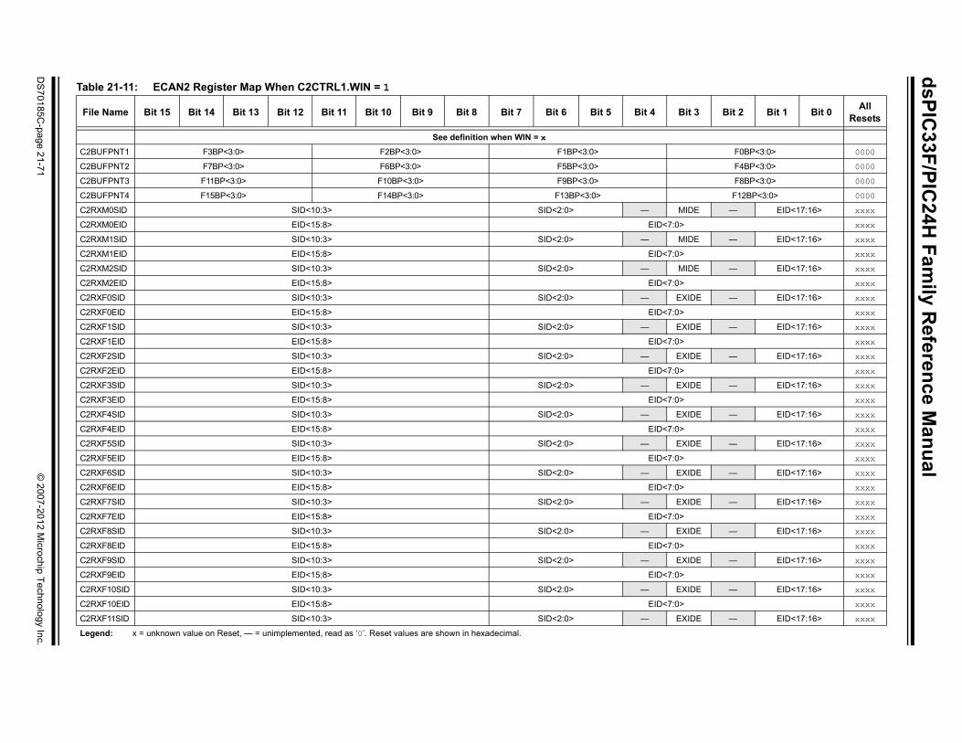
dsPIC33F/PIC
24H Fam
ily Reference M
anual
DS
70185C-page 21-71
© 2007-2012 M
icrochip Technology Inc.
Bit 3 Bit 2 Bit 1 Bit 0 All Resets
F0BP<3:0> 0000
F4BP<3:0> 0000
F8BP<3:0> 0000
F12BP<3:0> 0000
MIDE — EID<17:16> xxxx
<7:0> xxxx
MIDE — EID<17:16> xxxx
<7:0> xxxx
MIDE — EID<17:16> xxxx
<7:0> xxxx
EXIDE — EID<17:16> xxxx
<7:0> xxxx
EXIDE — EID<17:16> xxxx
<7:0> xxxx
EXIDE — EID<17:16> xxxx
<7:0> xxxx
EXIDE — EID<17:16> xxxx
<7:0> xxxx
EXIDE — EID<17:16> xxxx
<7:0> xxxx
EXIDE — EID<17:16> xxxx
<7:0> xxxx
EXIDE — EID<17:16> xxxx
<7:0> xxxx
EXIDE — EID<17:16> xxxx
<7:0> xxxx
EXIDE — EID<17:16> xxxx
<7:0> xxxx
EXIDE — EID<17:16> xxxx
<7:0> xxxx
EXIDE — EID<17:16> xxxx
<7:0> xxxx
EXIDE — EID<17:16> xxxx
Table 21-11: ECAN2 Register Map When C2CTRL1.WIN = 1
File Name Bit 15 Bit 14 Bit 13 Bit 12 Bit 11 Bit 10 Bit 9 Bit 8 Bit 7 Bit 6 Bit 5 Bit 4
See definition when WIN = xC2BUFPNT1 F3BP<3:0> F2BP<3:0> F1BP<3:0>
C2BUFPNT2 F7BP<3:0> F6BP<3:0> F5BP<3:0>
C2BUFPNT3 F11BP<3:0> F10BP<3:0> F9BP<3:0>
C2BUFPNT4 F15BP<3:0> F14BP<3:0> F13BP<3:0>
C2RXM0SID SID<10:3> SID<2:0> —
C2RXM0EID EID<15:8> EID
C2RXM1SID SID<10:3> SID<2:0> —
C2RXM1EID EID<15:8> EID
C2RXM2SID SID<10:3> SID<2:0> —
C2RXM2EID EID<15:8> EID
C2RXF0SID SID<10:3> SID<2:0> —
C2RXF0EID EID<15:8> EID
C2RXF1SID SID<10:3> SID<2:0> —
C2RXF1EID EID<15:8> EID
C2RXF2SID SID<10:3> SID<2:0> —
C2RXF2EID EID<15:8> EID
C2RXF3SID SID<10:3> SID<2:0> —
C2RXF3EID EID<15:8> EID
C2RXF4SID SID<10:3> SID<2:0> —
C2RXF4EID EID<15:8> EID
C2RXF5SID SID<10:3> SID<2:0> —
C2RXF5EID EID<15:8> EID
C2RXF6SID SID<10:3> SID<2:0> —
C2RXF6EID EID<15:8> EID
C2RXF7SID SID<10:3> SID<2:0> —
C2RXF7EID EID<15:8> EID
C2RXF8SID SID<10:3> SID<2:0> —
C2RXF8EID EID<15:8> EID
C2RXF9SID SID<10:3> SID<2:0> —
C2RXF9EID EID<15:8> EID
C2RXF10SID SID<10:3> SID<2:0> —
C2RXF10EID EID<15:8> EID
C2RXF11SID SID<10:3> SID<2:0> —
Legend: x = unknown value on Reset, — = unimplemented, read as ‘0’. Reset values are shown in hexadecimal.

dsPIC33F/PIC
24H Fam
ily Reference M
anual
DS
70185C-page 21-72
© 2007-2012 M
icrochip Technology Inc.
<7:0> xxxx
EXIDE — EID<17:16> xxxx
<7:0> xxxx
EXIDE — EID<17:16> xxxx
<7:0> xxxx
EXIDE — EID<17:16> xxxx
<7:0> xxxx
EXIDE — EID<17:16> xxxx
<7:0> xxxx
Bit 3 Bit 2 Bit 1 Bit 0 All Resets
C2RXF11EID EID<15:8> EID
C2RXF12SID SID<10:3> SID<2:0> —
C2RXF12EID EID<15:8> EID
C2RXF13SID SID<10:3> SID<2:0> —C2RXF13EID EID<15:8> EIDC2RXF14SID SID<10:3> SID<2:0> —C2RXF14EID EID<15:8> EIDC2RXF15SID SID<10:3> SID<2:0> —C2RXF15EID EID<15:8> EID
Table 21-11: ECAN2 Register Map When C2CTRL1.WIN = 1 (Continued)
File Name Bit 15 Bit 14 Bit 13 Bit 12 Bit 11 Bit 10 Bit 9 Bit 8 Bit 7 Bit 6 Bit 5 Bit 4
Legend: x = unknown value on Reset, — = unimplemented, read as ‘0’. Reset values are shown in hexadecimal.

Section 21. ECAN™EC
AN
™
21
21.15 RELATED APPLICATION NOTESThis section lists application notes that are related to this section of the manual. Theseapplication notes may not be written specifically for the dsPIC33F/PIC24H product family, but theconcepts are pertinent and could be used with modification and possible limitations. The currentapplication notes related to the Enhanced Controller Area Network (ECAN™) module are:
Title Application Note #No application notes at this time. N/A
Note: Please visit the Microchip web site (www.microchip.com) for additional ApplicationNotes and code examples for the dsPIC33F/PIC24H family of devices.
© 2007-2012 Microchip Technology Inc. DS70185C-page 21-73

dsPIC33F/PIC24H Family Reference Manual
21.16 REVISION HISTORY
Revision A (January 2007)This is the initial released version of the document.
Revision B (November 2009)This revision includes the following updates:
• Removed all references to the CANCKS bit in Figure 35-18, 35.9.4 “ECAN Bit Time Cal-culations”, Example 35-8, Example 35-9, Table 35-6 and Table 35-9.
• Examples:- Updated Example 35-1: Code Example for Standard Data Frame Transmission to
reflect the maximum CAN message size of 8 (0x0008). The example incorrectly stated the value of 15 (0x000F).
- Updated the code in Example 35-2: Code Example for Extended Data Frame Transmission to reflect message buffer 2 instead of message buffer 0
• Figures:- Updated the Logical value of SRR bit from ‘0’ to ‘1’ in Figure 35-5
• Notes:- Added a shaded note to 35.7.2.2 “Receiving Messages into Message Buffers 0-7”,
which details the effects of setting the TXREQ bit when the buffer is configured for receive operation
- Added a shaded note to 35.7.5 “DeviceNet™ Filtering”, which details operation constraints
- Added a shaded note to 35.11.3 “ECAN Event Interrupt”, which provides additional details on the highest priority CAN interrupt condition
• Registers:- Removed bit 11 (CANCKS) from CiFCTRL: ECAN™ FIFO Control Register (see
Register 35-18).- Changed the default value of R/W-0 to R/W-1 for FLTEN6-FLTEN15 in CiFEN1: ECAN
Acceptance Filter Enable Register (see Register 35-3)- Added shaded note to CiRXFnSID: ECAN Acceptance Filter Standard Identifier
Register (see Register 35-4)- F7MSK<1:0> = 11 was changed from “No Mask” to “Reserved” (see Register 35-8)- F15MSK<1:0> = 11 was changed from “No Mask” to “Reserved” (see Register 35-9)
• Sections:- Updated the Logical value of the SRR bit from ‘0’ to ‘1’ in 35.2.2 “Extended Data
Frame”- Removed the references to the WIN bit in 35.3.6 “ECAN Control and Error Counter
Registers”- Changed “CiERR” to “CiEC” in 35.10.2 “Fault Confinement”- Updated the Transmit Error Counter range in 35.10.2.4 “Transmitter in error
warning State”- Updated the Receive Error Counter range in 35.10.2.5 “Receiver in error warning
state”- Changed TXCAN to CiTX in 35.12.1 “Sleep Mode”- Completely revised 35.12.3 “Wake-up Functions”
• Additional minor corrections such as language and formatting updates have been incorporated throughout the document
DS70185C-page 21-74 © 2007-2012 Microchip Technology Inc.
Section 21. ECAN™EC
AN
™
21
Revision C (April 2012)This revision includes the following updates:• Updated 21.2.3 “Remote Frame”• Updated 21.6.3 “Remote Transmit Request/Response”• Updated Example 21-1• Updated Example 21-5• Updated Example 21-6• Updated Figure 21-19• Document was updated to include references to the PIC24H family of devices• Additional minor updated to text and formatting have been incorporated throughout the
document
© 2007-2012 Microchip Technology Inc. DS70185C-page 21-75

dsPIC33F/PIC24H Family Reference Manual
NOTES:
DS70185C-page 21-76 © 2007-2012 Microchip Technology Inc.

Note the following details of the code protection feature on Microchip devices:• Microchip products meet the specification contained in their particular Microchip Data Sheet.
• Microchip believes that its family of products is one of the most secure families of its kind on the market today, when used in the intended manner and under normal conditions.
• There are dishonest and possibly illegal methods used to breach the code protection feature. All of these methods, to our knowledge, require using the Microchip products in a manner outside the operating specifications contained in Microchip’s Data Sheets. Most likely, the person doing so is engaged in theft of intellectual property.
• Microchip is willing to work with the customer who is concerned about the integrity of their code.
• Neither Microchip nor any other semiconductor manufacturer can guarantee the security of their code. Code protection does not mean that we are guaranteeing the product as “unbreakable.”
Code protection is constantly evolving. We at Microchip are committed to continuously improving the code protection features of ourproducts. Attempts to break Microchip’s code protection feature may be a violation of the Digital Millennium Copyright Act. If such actsallow unauthorized access to your software or other copyrighted work, you may have a right to sue for relief under that Act.
Information contained in this publication regarding deviceapplications and the like is provided only for your convenienceand may be superseded by updates. It is your responsibility toensure that your application meets with your specifications.MICROCHIP MAKES NO REPRESENTATIONS ORWARRANTIES OF ANY KIND WHETHER EXPRESS ORIMPLIED, WRITTEN OR ORAL, STATUTORY OROTHERWISE, RELATED TO THE INFORMATION,INCLUDING BUT NOT LIMITED TO ITS CONDITION,QUALITY, PERFORMANCE, MERCHANTABILITY ORFITNESS FOR PURPOSE. Microchip disclaims all liabilityarising from this information and its use. Use of Microchipdevices in life support and/or safety applications is entirely atthe buyer’s risk, and the buyer agrees to defend, indemnify andhold harmless Microchip from any and all damages, claims,suits, or expenses resulting from such use. No licenses areconveyed, implicitly or otherwise, under any Microchipintellectual property rights.
© 2007-2012 Microchip Technology Inc.
QUALITY MANAGEMENT SYSTEM CERTIFIED BY DNV
== ISO/TS 16949 ==
Trademarks
The Microchip name and logo, the Microchip logo, dsPIC, KEELOQ, KEELOQ logo, MPLAB, PIC, PICmicro, PICSTART, PIC32 logo, rfPIC and UNI/O are registered trademarks of Microchip Technology Incorporated in the U.S.A. and other countries.
FilterLab, Hampshire, HI-TECH C, Linear Active Thermistor, MXDEV, MXLAB, SEEVAL and The Embedded Control Solutions Company are registered trademarks of Microchip Technology Incorporated in the U.S.A.
Analog-for-the-Digital Age, Application Maestro, chipKIT, chipKIT logo, CodeGuard, dsPICDEM, dsPICDEM.net, dsPICworks, dsSPEAK, ECAN, ECONOMONITOR, FanSense, HI-TIDE, In-Circuit Serial Programming, ICSP, Mindi, MiWi, MPASM, MPLAB Certified logo, MPLIB, MPLINK, mTouch, Omniscient Code Generation, PICC, PICC-18, PICDEM, PICDEM.net, PICkit, PICtail, REAL ICE, rfLAB, Select Mode, Total Endurance, TSHARC, UniWinDriver, WiperLock and ZENA are trademarks of Microchip Technology Incorporated in the U.S.A. and other countries.
SQTP is a service mark of Microchip Technology Incorporated in the U.S.A.
All other trademarks mentioned herein are property of their respective companies.
© 2007-2012, Microchip Technology Incorporated, Printed in the U.S.A., All Rights Reserved.
Printed on recycled paper.
ISBN: 978-1-62076-230-1
DS70185C-page 21-77
Microchip received ISO/TS-16949:2009 certification for its worldwide headquarters, design and wafer fabrication facilities in Chandler and Tempe, Arizona; Gresham, Oregon and design centers in California and India. The Company’s quality system processes and procedures are for its PIC® MCUs and dsPIC® DSCs, KEELOQ® code hopping devices, Serial EEPROMs, microperipherals, nonvolatile memory and analog products. In addition, Microchip’s quality system for the design and manufacture of development systems is ISO 9001:2000 certified.

DS70185C-page 21-78 © 2007-2012 Microchip Technology Inc.
AMERICASCorporate Office2355 West Chandler Blvd.Chandler, AZ 85224-6199Tel: 480-792-7200 Fax: 480-792-7277Technical Support: http://www.microchip.com/supportWeb Address: www.microchip.comAtlantaDuluth, GA Tel: 678-957-9614 Fax: 678-957-1455BostonWestborough, MA Tel: 774-760-0087 Fax: 774-760-0088ChicagoItasca, IL Tel: 630-285-0071 Fax: 630-285-0075ClevelandIndependence, OH Tel: 216-447-0464 Fax: 216-447-0643DallasAddison, TX Tel: 972-818-7423 Fax: 972-818-2924DetroitFarmington Hills, MI Tel: 248-538-2250Fax: 248-538-2260IndianapolisNoblesville, IN Tel: 317-773-8323Fax: 317-773-5453Los AngelesMission Viejo, CA Tel: 949-462-9523 Fax: 949-462-9608Santa ClaraSanta Clara, CA Tel: 408-961-6444Fax: 408-961-6445TorontoMississauga, Ontario, CanadaTel: 905-673-0699 Fax: 905-673-6509
ASIA/PACIFICAsia Pacific OfficeSuites 3707-14, 37th FloorTower 6, The GatewayHarbour City, KowloonHong KongTel: 852-2401-1200Fax: 852-2401-3431Australia - SydneyTel: 61-2-9868-6733Fax: 61-2-9868-6755China - BeijingTel: 86-10-8569-7000 Fax: 86-10-8528-2104China - ChengduTel: 86-28-8665-5511Fax: 86-28-8665-7889China - ChongqingTel: 86-23-8980-9588Fax: 86-23-8980-9500China - HangzhouTel: 86-571-2819-3187 Fax: 86-571-2819-3189China - Hong Kong SARTel: 852-2401-1200 Fax: 852-2401-3431China - NanjingTel: 86-25-8473-2460Fax: 86-25-8473-2470China - QingdaoTel: 86-532-8502-7355Fax: 86-532-8502-7205China - ShanghaiTel: 86-21-5407-5533 Fax: 86-21-5407-5066China - ShenyangTel: 86-24-2334-2829Fax: 86-24-2334-2393China - ShenzhenTel: 86-755-8203-2660 Fax: 86-755-8203-1760China - WuhanTel: 86-27-5980-5300Fax: 86-27-5980-5118China - XianTel: 86-29-8833-7252Fax: 86-29-8833-7256China - XiamenTel: 86-592-2388138 Fax: 86-592-2388130China - ZhuhaiTel: 86-756-3210040 Fax: 86-756-3210049
ASIA/PACIFICIndia - BangaloreTel: 91-80-3090-4444 Fax: 91-80-3090-4123India - New DelhiTel: 91-11-4160-8631Fax: 91-11-4160-8632India - PuneTel: 91-20-2566-1512Fax: 91-20-2566-1513Japan - OsakaTel: 81-66-152-7160 Fax: 81-66-152-9310Japan - YokohamaTel: 81-45-471- 6166 Fax: 81-45-471-6122Korea - DaeguTel: 82-53-744-4301Fax: 82-53-744-4302Korea - SeoulTel: 82-2-554-7200Fax: 82-2-558-5932 or 82-2-558-5934Malaysia - Kuala LumpurTel: 60-3-6201-9857Fax: 60-3-6201-9859Malaysia - PenangTel: 60-4-227-8870Fax: 60-4-227-4068Philippines - ManilaTel: 63-2-634-9065Fax: 63-2-634-9069SingaporeTel: 65-6334-8870Fax: 65-6334-8850Taiwan - Hsin ChuTel: 886-3-5778-366Fax: 886-3-5770-955Taiwan - KaohsiungTel: 886-7-536-4818Fax: 886-7-330-9305Taiwan - TaipeiTel: 886-2-2500-6610 Fax: 886-2-2508-0102Thailand - BangkokTel: 66-2-694-1351Fax: 66-2-694-1350
EUROPEAustria - WelsTel: 43-7242-2244-39Fax: 43-7242-2244-393Denmark - CopenhagenTel: 45-4450-2828 Fax: 45-4485-2829France - ParisTel: 33-1-69-53-63-20 Fax: 33-1-69-30-90-79Germany - MunichTel: 49-89-627-144-0 Fax: 49-89-627-144-44Italy - Milan Tel: 39-0331-742611 Fax: 39-0331-466781Netherlands - DrunenTel: 31-416-690399 Fax: 31-416-690340Spain - MadridTel: 34-91-708-08-90Fax: 34-91-708-08-91UK - WokinghamTel: 44-118-921-5869Fax: 44-118-921-5820
Worldwide Sales and Service
11/29/11