Embed Size (px)
Citation preview
ESE 499 – Feedback Control Systems
SECTION 10: FREQUENCY-RESPONSE DESIGN
K. Webb ESE 499
2
Introduction
We have seen how to design feedback control systems using the root locus
In this section of the course, we’ll learn how to do the same using the open-loop frequency response
Objectives: Determine static error constants from the open-loop
frequency response Determine closed-loop stability from the open-loop
frequency response Use the open-loop frequency response for compensator
design to: Improve steady-state error Improve transient response
K. Webb ESE 499
Steady-State Error from Bode Plots3
K. Webb ESE 499
4
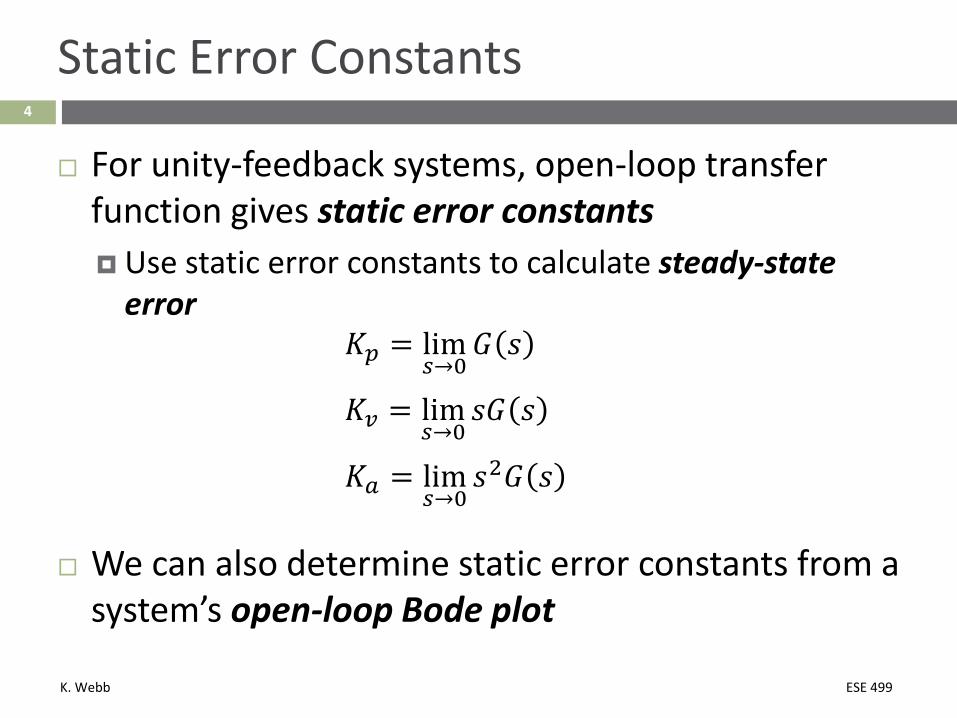
Static Error Constants
For unity-feedback systems, open-loop transfer function gives static error constants Use static error constants to calculate steady-state
error𝐾𝐾𝑝𝑝 = lim
𝑠𝑠→0𝐺𝐺 𝑠𝑠
𝐾𝐾𝑣𝑣 = lim𝑠𝑠→0
𝑠𝑠𝐺𝐺 𝑠𝑠
𝐾𝐾𝑎𝑎 = lim𝑠𝑠→0
𝑠𝑠2𝐺𝐺 𝑠𝑠
We can also determine static error constants from a system’s open-loop Bode plot
K. Webb ESE 499
5
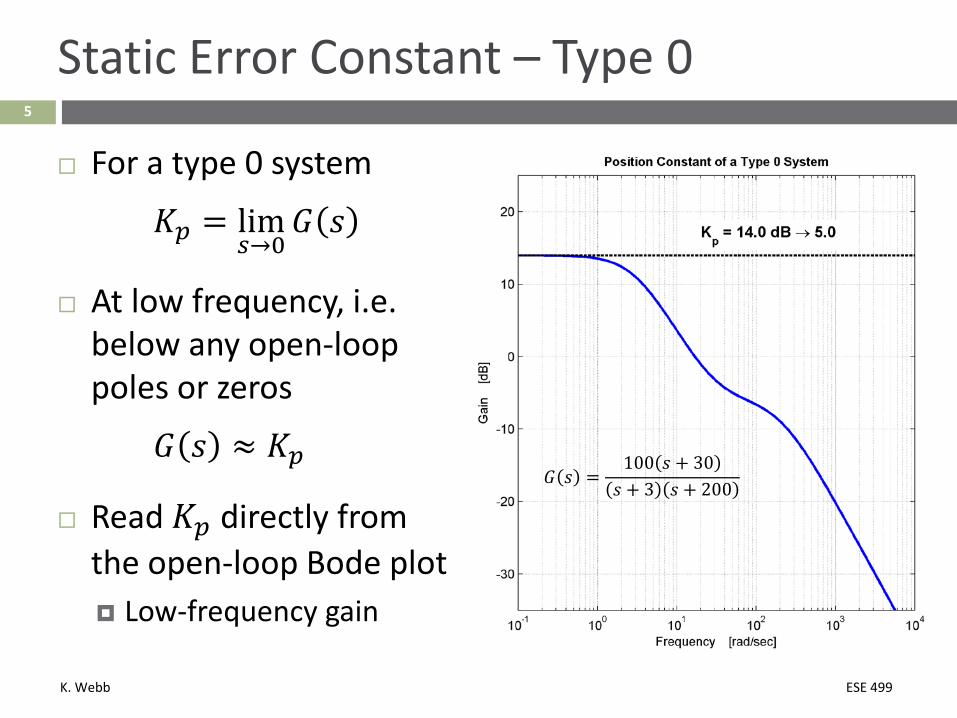
Static Error Constant – Type 0
For a type 0 system
𝐾𝐾𝑝𝑝 = lim𝑠𝑠→0
𝐺𝐺 𝑠𝑠
At low frequency, i.e. below any open-loop poles or zeros
𝐺𝐺 𝑠𝑠 ≈ 𝐾𝐾𝑝𝑝
Read 𝐾𝐾𝑝𝑝 directly from the open-loop Bode plot Low-frequency gain
𝐺𝐺 𝑠𝑠 =100 𝑠𝑠 + 30𝑠𝑠 + 3 𝑠𝑠 + 200
K. Webb ESE 499
6
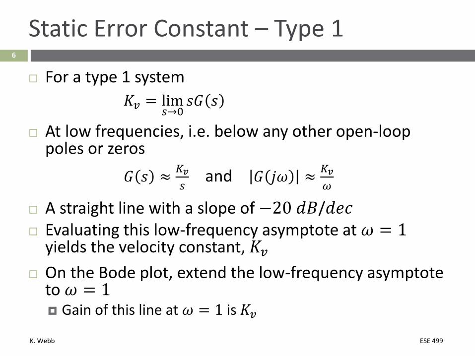
Static Error Constant – Type 1
For a type 1 system𝐾𝐾𝑣𝑣 = lim
𝑠𝑠→0𝑠𝑠𝐺𝐺 𝑠𝑠
At low frequencies, i.e. below any other open-loop poles or zeros
𝐺𝐺 𝑠𝑠 ≈ 𝐾𝐾𝑣𝑣𝑠𝑠
and 𝐺𝐺 𝑗𝑗𝑗𝑗 ≈ 𝐾𝐾𝑣𝑣𝜔𝜔
A straight line with a slope of −20 𝑑𝑑𝑑𝑑/𝑑𝑑𝑑𝑑𝑑𝑑 Evaluating this low-frequency asymptote at 𝑗𝑗 = 1
yields the velocity constant, 𝐾𝐾𝑣𝑣 On the Bode plot, extend the low-frequency asymptote
to 𝑗𝑗 = 1 Gain of this line at 𝑗𝑗 = 1 is 𝐾𝐾𝑣𝑣
K. Webb ESE 499
7
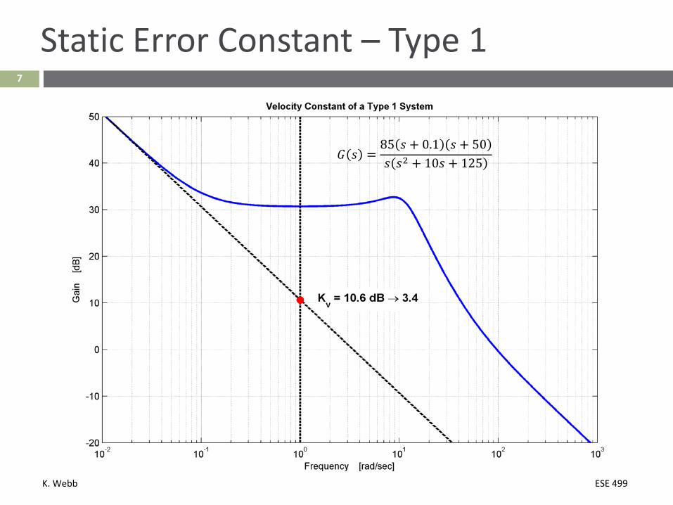
Static Error Constant – Type 1
𝐺𝐺 𝑠𝑠 =85 𝑠𝑠 + 0.1 𝑠𝑠 + 50𝑠𝑠 𝑠𝑠2 + 10𝑠𝑠 + 125
K. Webb ESE 499
8
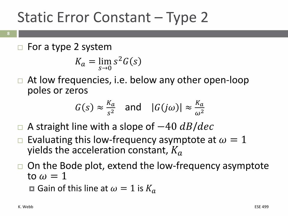
Static Error Constant – Type 2
For a type 2 system𝐾𝐾𝑎𝑎 = lim
𝑠𝑠→0𝑠𝑠2𝐺𝐺 𝑠𝑠
At low frequencies, i.e. below any other open-loop poles or zeros
𝐺𝐺 𝑠𝑠 ≈ 𝐾𝐾𝑎𝑎𝑠𝑠2
and 𝐺𝐺 𝑗𝑗𝑗𝑗 ≈ 𝐾𝐾𝑎𝑎𝜔𝜔2
A straight line with a slope of −40 𝑑𝑑𝑑𝑑/𝑑𝑑𝑑𝑑𝑑𝑑 Evaluating this low-frequency asymptote at 𝑗𝑗 = 1
yields the acceleration constant, 𝐾𝐾𝑎𝑎 On the Bode plot, extend the low-frequency asymptote
to 𝑗𝑗 = 1 Gain of this line at 𝑗𝑗 = 1 is 𝐾𝐾𝑎𝑎
K. Webb ESE 499
9
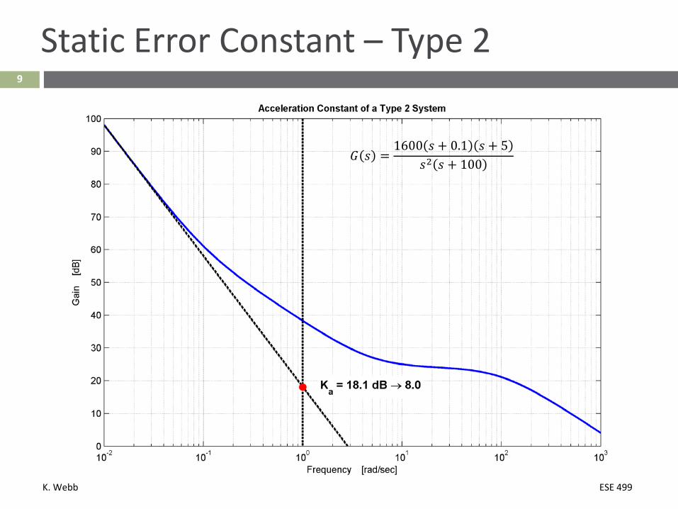
Static Error Constant – Type 2
𝐺𝐺 𝑠𝑠 =1600 𝑠𝑠 + 0.1 𝑠𝑠 + 5
𝑠𝑠2 𝑠𝑠 + 100
K. Webb ESE 499
Stability from Open-Loop Bode Plots10
K. Webb ESE 499
11
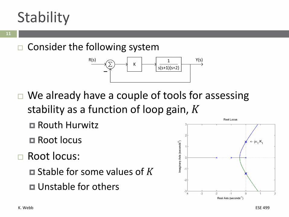
Stability
Consider the following system
We already have a couple of tools for assessing stability as a function of loop gain, 𝐾𝐾 Routh Hurwitz Root locus
Root locus: Stable for some values of 𝐾𝐾 Unstable for others
K. Webb ESE 499
12
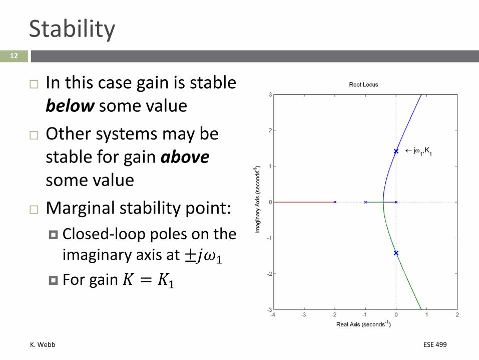
Stability
In this case gain is stable below some value
Other systems may be stable for gain abovesome value
Marginal stability point: Closed-loop poles on the
imaginary axis at ±𝑗𝑗𝑗𝑗1 For gain 𝐾𝐾 = 𝐾𝐾1
K. Webb ESE 499
13
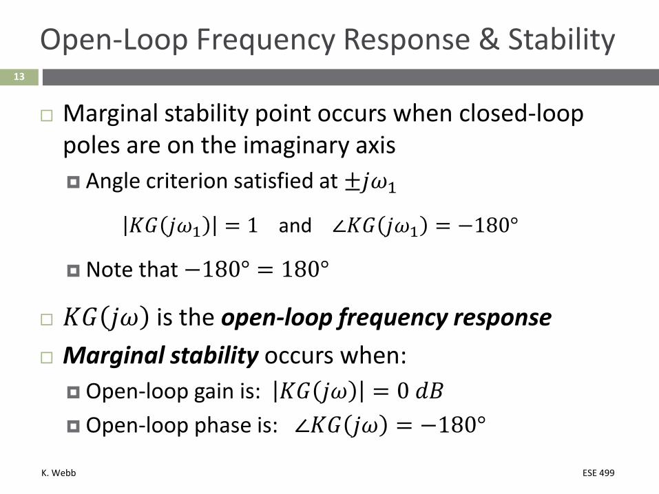
Open-Loop Frequency Response & Stability
Marginal stability point occurs when closed-loop poles are on the imaginary axis Angle criterion satisfied at ±𝑗𝑗𝑗𝑗1
𝐾𝐾𝐺𝐺 𝑗𝑗𝑗𝑗1 = 1 and ∠𝐾𝐾𝐺𝐺 𝑗𝑗𝑗𝑗1 = −180°
Note that −180° = 180°
𝐾𝐾𝐺𝐺 𝑗𝑗𝑗𝑗 is the open-loop frequency response Marginal stability occurs when:
Open-loop gain is: 𝐾𝐾𝐺𝐺 𝑗𝑗𝑗𝑗 = 0 𝑑𝑑𝑑𝑑 Open-loop phase is: ∠𝐾𝐾𝐺𝐺 𝑗𝑗𝑗𝑗 = −180°
K. Webb ESE 499
14
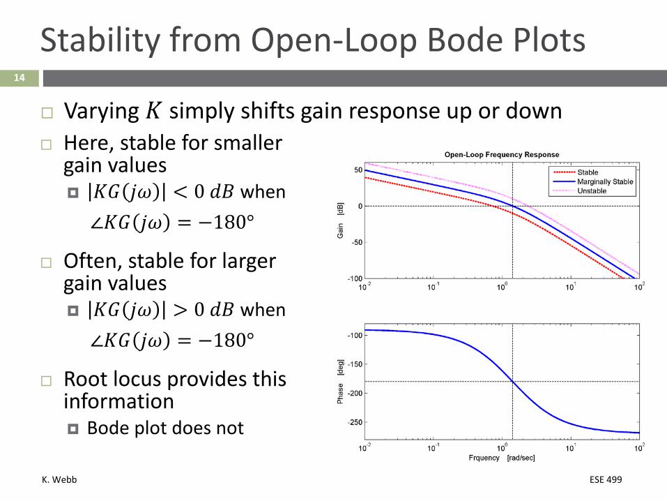
Stability from Open-Loop Bode Plots
Here, stable for smaller gain values 𝐾𝐾𝐺𝐺 𝑗𝑗𝑗𝑗 < 0 𝑑𝑑𝑑𝑑 when∠𝐾𝐾𝐺𝐺 𝑗𝑗𝑗𝑗 = −180°
Often, stable for larger gain values 𝐾𝐾𝐺𝐺 𝑗𝑗𝑗𝑗 > 0 𝑑𝑑𝑑𝑑 when∠𝐾𝐾𝐺𝐺 𝑗𝑗𝑗𝑗 = −180°
Root locus provides this information Bode plot does not
Varying 𝐾𝐾 simply shifts gain response up or down
K. Webb ESE 499
15
Open-Loop Frequency Response & Stability
Open-loop Bode plot can be used to assess stability But, we need to know if system is closed-loop stable for low gain
or high gain
Here, we’ll assume open-loop-stable systems Closed-loop stable for low gain
Open-loop Bode plot can tell us: Is a system closed-loop stable? If so, how stable? I.e. how close to marginal stability
Two stability metrics: Gain margin Phase margin
K. Webb ESE 499
Stability Margins16
K. Webb ESE 499
17
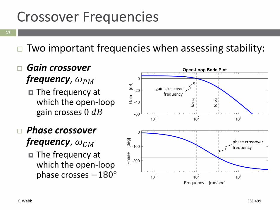
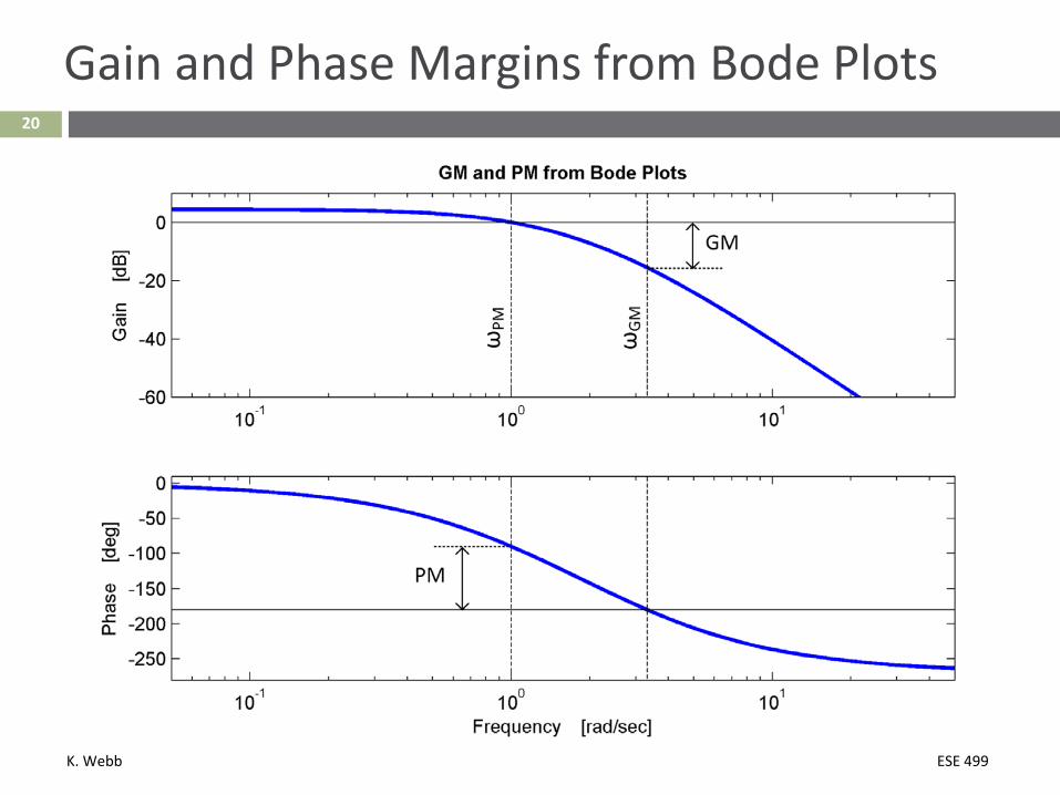
Crossover Frequencies
Two important frequencies when assessing stability:
Gain crossover frequency, 𝑗𝑗𝑃𝑃𝑃𝑃 The frequency at
which the open-loop gain crosses 0 𝑑𝑑𝑑𝑑
Phase crossover frequency, 𝑗𝑗𝐺𝐺𝑃𝑃 The frequency at
which the open-loop phase crosses −180°
K. Webb ESE 499
18
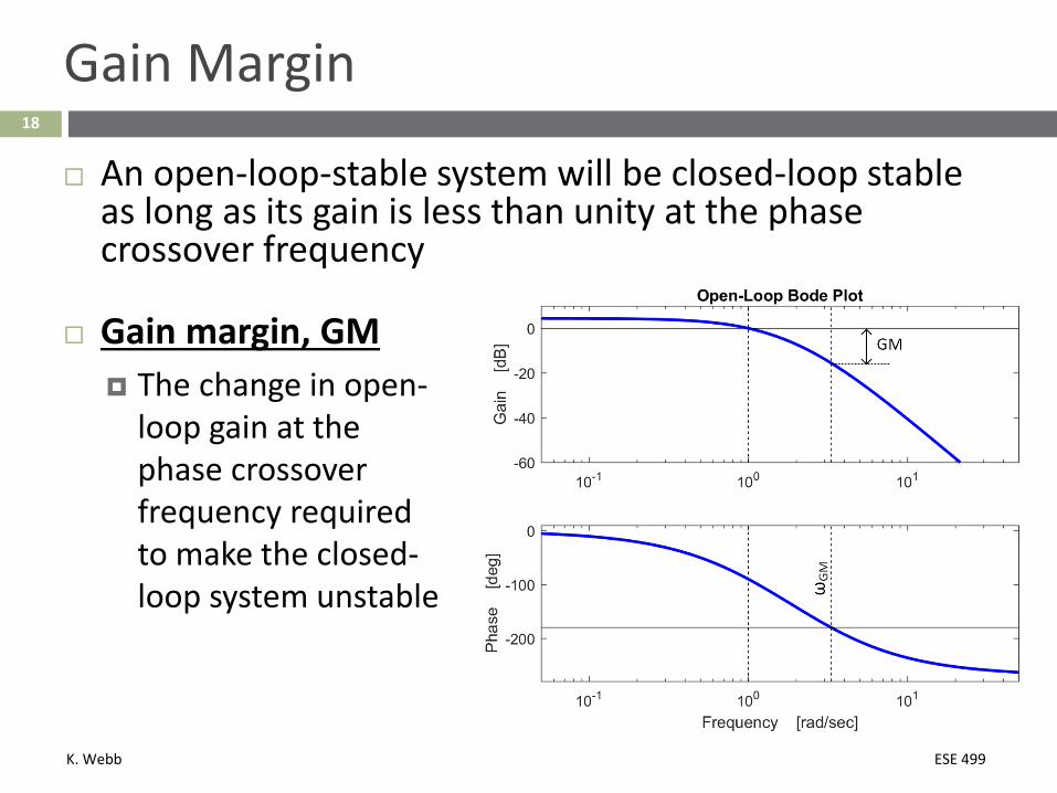
Gain Margin
An open-loop-stable system will be closed-loop stable as long as its gain is less than unity at the phase crossover frequency
Gain margin, GM The change in open-
loop gain at the phase crossover frequency required to make the closed-loop system unstable
K. Webb ESE 499
19
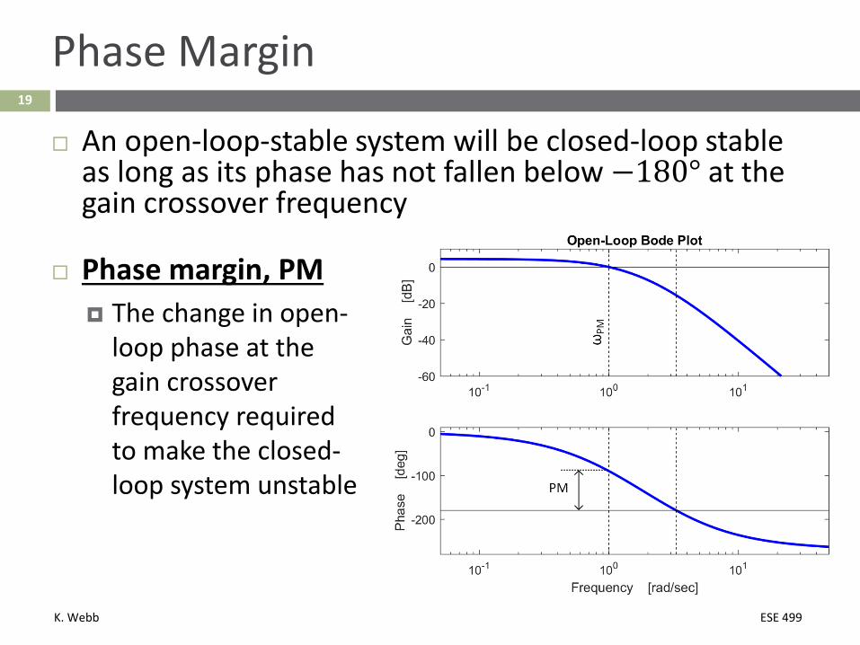
Phase Margin
An open-loop-stable system will be closed-loop stable as long as its phase has not fallen below −180° at the gain crossover frequency
Phase margin, PM The change in open-
loop phase at the gain crossover frequency required to make the closed-loop system unstable
K. Webb ESE 499
20
Gain and Phase Margins from Bode Plots
K. Webb ESE 499
21
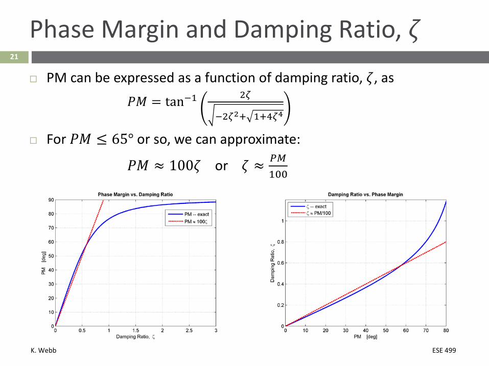
Phase Margin and Damping Ratio, 𝜁𝜁 PM can be expressed as a function of damping ratio, 𝜁𝜁, as
𝑃𝑃𝑃𝑃 = tan−1 2𝜁𝜁
−2𝜁𝜁2+ 1+4𝜁𝜁4
For 𝑃𝑃𝑃𝑃 ≤ 65° or so, we can approximate:
𝑃𝑃𝑃𝑃 ≈ 100𝜁𝜁 or 𝜁𝜁 ≈ 𝑃𝑃𝑃𝑃100
K. Webb ESE 499
Frequency Response Analysis in MATLAB22
K. Webb ESE 499
23
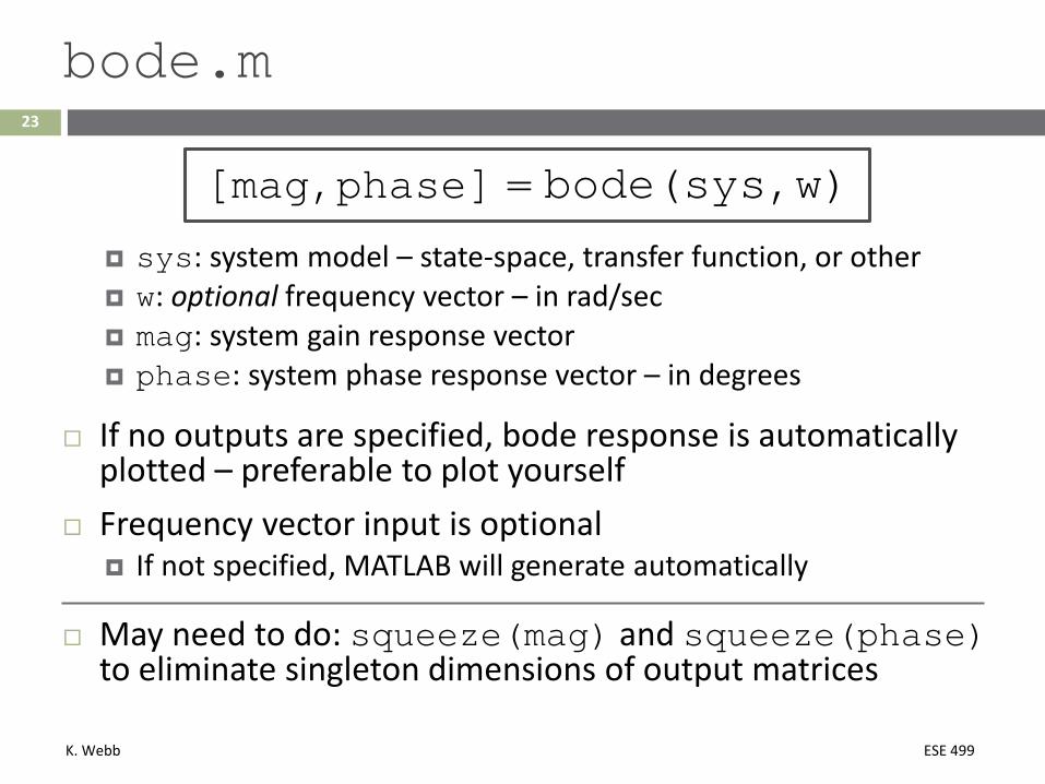
bode.m
[mag,phase] = bode(sys,w)
sys: system model – state-space, transfer function, or other w: optional frequency vector – in rad/sec mag: system gain response vector phase: system phase response vector – in degrees
If no outputs are specified, bode response is automatically plotted – preferable to plot yourself
Frequency vector input is optional If not specified, MATLAB will generate automatically
May need to do: squeeze(mag) and squeeze(phase)to eliminate singleton dimensions of output matrices
K. Webb ESE 499
24
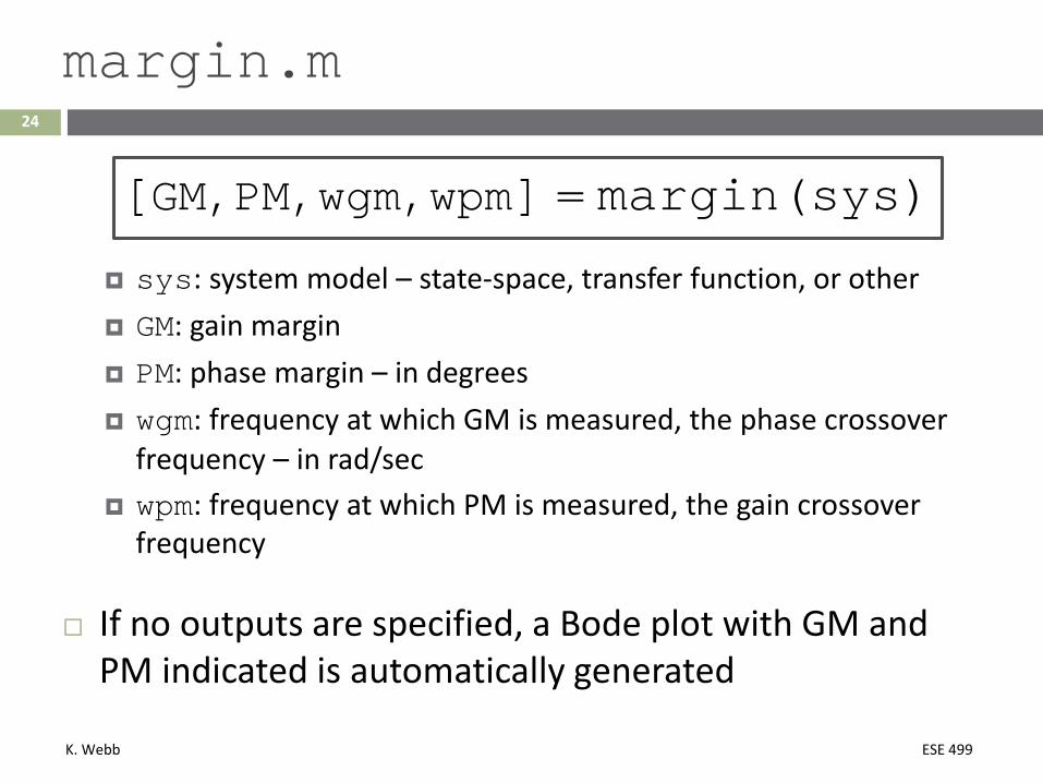
margin.m
[GM,PM,wgm,wpm] = margin(sys)
sys: system model – state-space, transfer function, or other GM: gain margin PM: phase margin – in degrees wgm: frequency at which GM is measured, the phase crossover
frequency – in rad/sec wpm: frequency at which PM is measured, the gain crossover
frequency
If no outputs are specified, a Bode plot with GM and PM indicated is automatically generated
K. Webb ESE 499
Frequency-Response Design25
K. Webb ESE 499
26
Frequency-Response Design
In a previous section of notes, we saw how we can use root-locus techniques to design compensators
Two primary objectives of compensation Improve steady-state error Proportional-integral (PI) compensation Lag compensation
Improve dynamic response Proportional-derivative (PD) compensation Lead compensation
Now, we’ll learn to design compensators using a system’s open-loop frequency response We’ll focus on lag and lead compensation
K. Webb ESE 499
Improving Steady-State Error27
K. Webb ESE 499
28
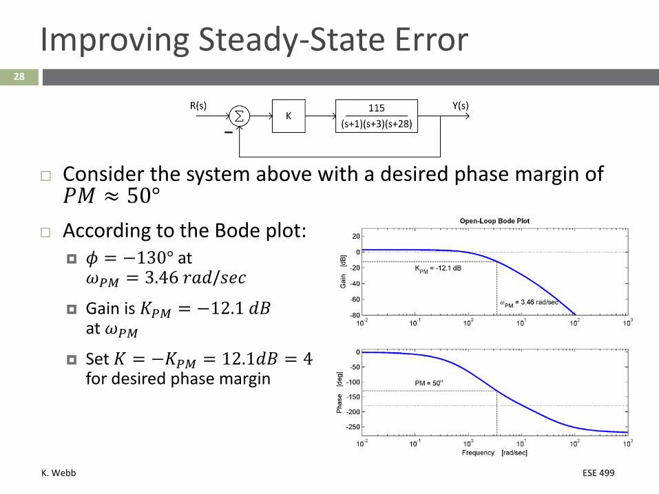
Improving Steady-State Error
Consider the system above with a desired phase margin of 𝑃𝑃𝑃𝑃 ≈ 50°
According to the Bode plot: 𝜙𝜙 = −130° at 𝑗𝑗𝑃𝑃𝑃𝑃 = 3.46 𝑟𝑟𝑟𝑟𝑑𝑑/𝑠𝑠𝑑𝑑𝑑𝑑
Gain is 𝐾𝐾𝑃𝑃𝑃𝑃 = −12.1 𝑑𝑑𝑑𝑑at 𝑗𝑗𝑃𝑃𝑃𝑃
Set 𝐾𝐾 = −𝐾𝐾𝑃𝑃𝑃𝑃 = 12.1𝑑𝑑𝑑𝑑 = 4for desired phase margin
K. Webb ESE 499
29
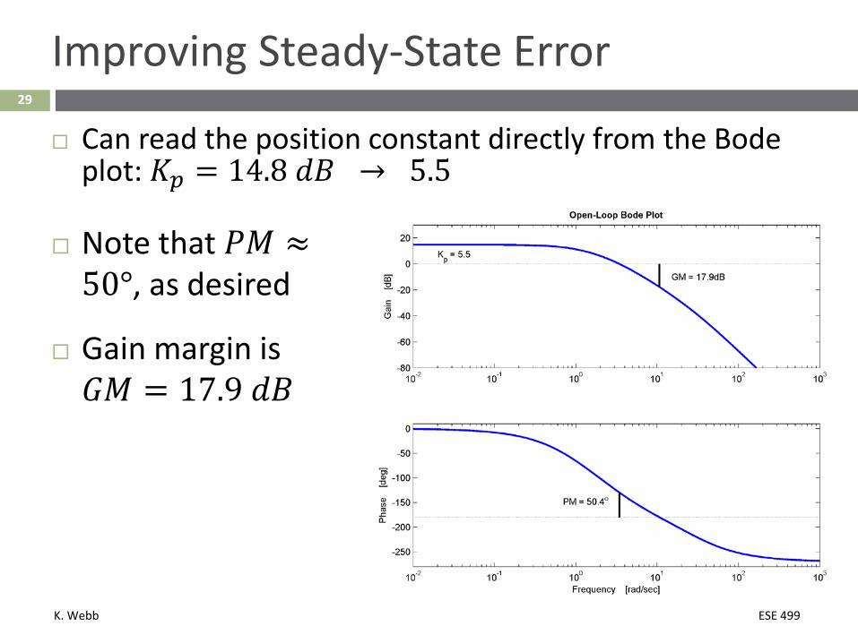
Improving Steady-State Error
Can read the position constant directly from the Bode plot: 𝐾𝐾𝑝𝑝 = 14.8 𝑑𝑑𝑑𝑑 → 5.5
Note that 𝑃𝑃𝑃𝑃 ≈50°, as desired
Gain margin is 𝐺𝐺𝑃𝑃 = 17.9 𝑑𝑑𝑑𝑑
K. Webb ESE 499
30
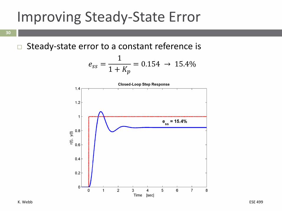
Improving Steady-State Error
Steady-state error to a constant reference is
𝑑𝑑𝑠𝑠𝑠𝑠 =1
1 + 𝐾𝐾𝑝𝑝= 0.154 → 15.4%
K. Webb ESE 499
31
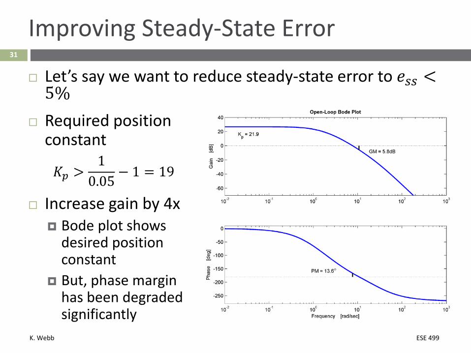
Improving Steady-State Error
Let’s say we want to reduce steady-state error to 𝑑𝑑𝑠𝑠𝑠𝑠 <5%
Required position constant
𝐾𝐾𝑝𝑝 >1
0.05 − 1 = 19
Increase gain by 4x Bode plot shows
desired position constant
But, phase margin has been degraded significantly
K. Webb ESE 499
32
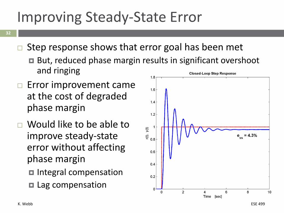
Improving Steady-State Error
Step response shows that error goal has been met But, reduced phase margin results in significant overshoot
and ringing Error improvement came
at the cost of degraded phase margin
Would like to be able to improve steady-state error without affecting phase margin Integral compensation Lag compensation
K. Webb ESE 499
Integral Compensation33
K. Webb ESE 499
34
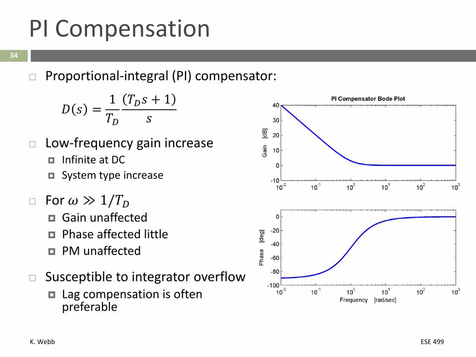
PI Compensation
Proportional-integral (PI) compensator:
𝐷𝐷 𝑠𝑠 =1𝑇𝑇𝐷𝐷
𝑇𝑇𝐷𝐷𝑠𝑠 + 1𝑠𝑠
Low-frequency gain increase Infinite at DC System type increase
For 𝑗𝑗 ≫ 1/𝑇𝑇𝐷𝐷 Gain unaffected Phase affected little PM unaffected
Susceptible to integrator overflow Lag compensation is often
preferable

K. Webb ESE 499
Lag Compensation35
K. Webb ESE 499
36
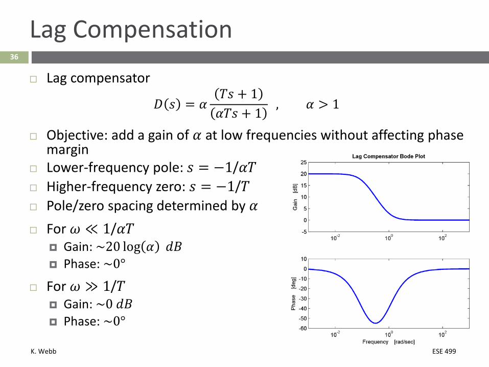
Lag Compensation
Lag compensator
𝐷𝐷 𝑠𝑠 = 𝛼𝛼𝑇𝑇𝑠𝑠 + 1𝛼𝛼𝑇𝑇𝑠𝑠 + 1
, 𝛼𝛼 > 1
Objective: add a gain of 𝛼𝛼 at low frequencies without affecting phase margin
Lower-frequency pole: 𝑠𝑠 = −1/𝛼𝛼𝑇𝑇 Higher-frequency zero: 𝑠𝑠 = −1/𝑇𝑇 Pole/zero spacing determined by 𝛼𝛼 For 𝑗𝑗 ≪ 1/𝛼𝛼𝑇𝑇
Gain: ~20 log 𝛼𝛼 𝑑𝑑𝑑𝑑 Phase: ~0°
For 𝑗𝑗 ≫ 1/𝑇𝑇 Gain: ~0 𝑑𝑑𝑑𝑑 Phase: ~0°
K. Webb ESE 499
37
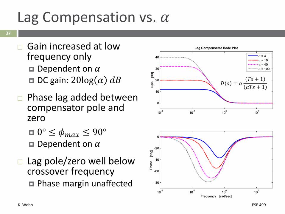
Lag Compensation vs. 𝛼𝛼
Gain increased at low frequency only Dependent on 𝛼𝛼 DC gain: 20log 𝛼𝛼 𝑑𝑑𝑑𝑑
Phase lag added between compensator pole and zero 0° ≤ 𝜙𝜙𝑚𝑚𝑎𝑎𝑚𝑚 ≤ 90° Dependent on 𝛼𝛼
Lag pole/zero well below crossover frequency Phase margin unaffected
𝐷𝐷 𝑠𝑠 = 𝛼𝛼𝑇𝑇𝑠𝑠 + 1𝛼𝛼𝑇𝑇𝑠𝑠 + 1
K. Webb ESE 499
38
Lag Compensator Design Procedure
Lag compensator adds gain at low frequencies without affecting phase margin
Basic design procedure: Adjust gain to achieve the desired phase margin Add compensation, increasing low-frequency gain to
achieve desired error performance
Same as adjusting gain to place poles at the desired damping on the root locus, then adding compensation Root locus is not changed Here, the frequency response near the crossover frequency
is not changed
K. Webb ESE 499
39
Lag Compensator Design Procedure
1. Adjust gain, 𝐾𝐾, of the uncompensated system to provide the desired phase margin plus 5° … 10° (to account for small phase lag added by compensator)
2. Use the open-loop Bode plot for the uncompensated system with the value of gain set in the previous step to determine the static error constant
3. Calculate 𝜶𝜶 as the low-frequency gain increase required to provide the desired error performance
4. Set the upper corner frequency (the zero) to be one decade below the crossover frequency: 1/𝑇𝑇 = 𝑗𝑗𝑃𝑃𝑃𝑃/10 Minimizes the added phase lag at the crossover frequency
5. Calculate the lag pole: 1/𝛼𝛼𝑇𝑇6. Simulate and iterate, if necessary
K. Webb ESE 499
40
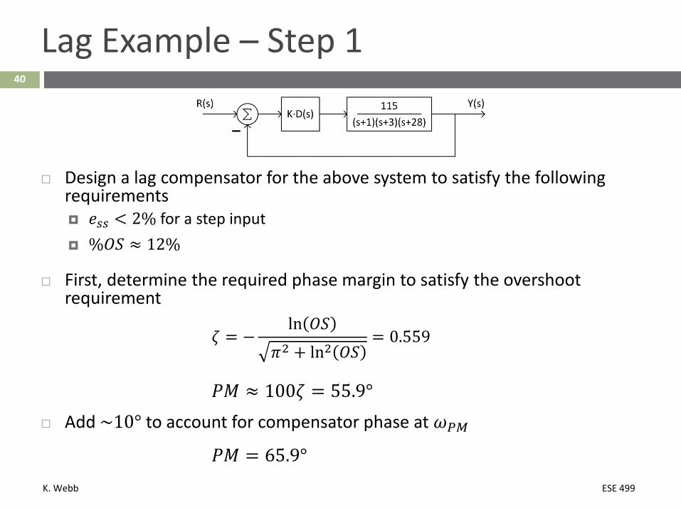
Lag Example – Step 1
Design a lag compensator for the above system to satisfy the following requirements 𝑑𝑑𝑠𝑠𝑠𝑠 < 2% for a step input %𝑂𝑂𝑂𝑂 ≈ 12%
First, determine the required phase margin to satisfy the overshoot requirement
𝜁𝜁 = −ln 𝑂𝑂𝑂𝑂
𝜋𝜋2 + ln2 𝑂𝑂𝑂𝑂= 0.559
𝑃𝑃𝑃𝑃 ≈ 100𝜁𝜁 = 55.9° Add ~10° to account for compensator phase at 𝑗𝑗𝑃𝑃𝑃𝑃
𝑃𝑃𝑃𝑃 = 65.9°
K. Webb ESE 499
41
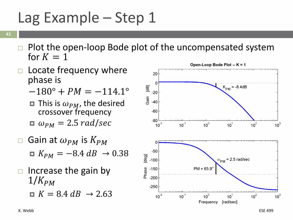
Lag Example – Step 1
Plot the open-loop Bode plot of the uncompensated system for 𝐾𝐾 = 1
Locate frequency where phase is−180° + 𝑃𝑃𝑃𝑃 = −114.1° This is 𝑗𝑗𝑃𝑃𝑃𝑃, the desired
crossover frequency 𝑗𝑗𝑃𝑃𝑃𝑃 = 2.5 𝑟𝑟𝑟𝑟𝑑𝑑/𝑠𝑠𝑑𝑑𝑑𝑑
Gain at 𝑗𝑗𝑃𝑃𝑃𝑃 is 𝐾𝐾𝑃𝑃𝑃𝑃 𝐾𝐾𝑃𝑃𝑃𝑃 = −8.4 𝑑𝑑𝑑𝑑 → 0.38
Increase the gain by 1/𝐾𝐾𝑃𝑃𝑃𝑃 𝐾𝐾 = 8.4 𝑑𝑑𝑑𝑑 → 2.63
K. Webb ESE 499
42
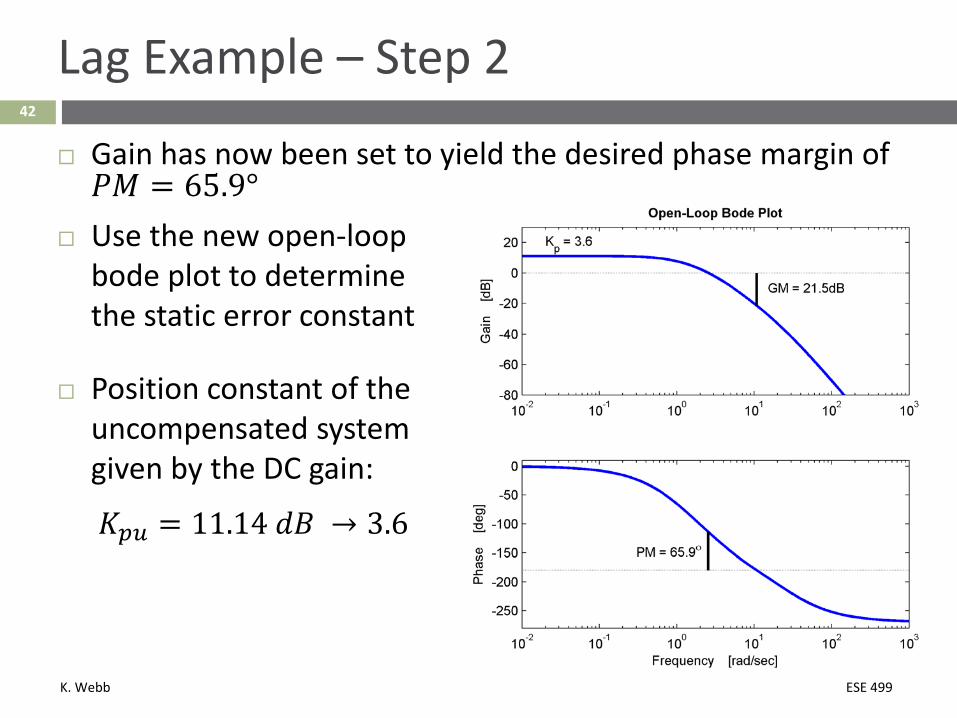
Lag Example – Step 2
Gain has now been set to yield the desired phase margin of 𝑃𝑃𝑃𝑃 = 65.9°
Use the new open-loop bode plot to determine the static error constant
Position constant of the uncompensated system given by the DC gain:
𝐾𝐾𝑝𝑝𝑝𝑝 = 11.14 𝑑𝑑𝑑𝑑 → 3.6
K. Webb ESE 499
43
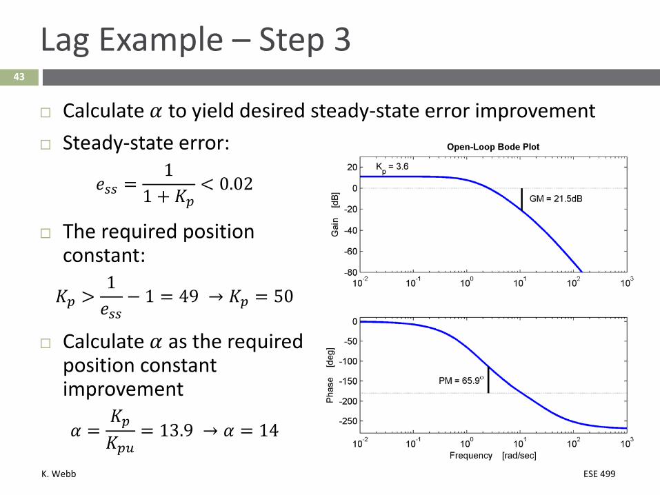
Lag Example – Step 3
Calculate 𝛼𝛼 to yield desired steady-state error improvement Steady-state error:
𝑑𝑑𝑠𝑠𝑠𝑠 =1
1 + 𝐾𝐾𝑝𝑝< 0.02
The required position constant:
𝐾𝐾𝑝𝑝 >1𝑑𝑑𝑠𝑠𝑠𝑠
− 1 = 49 → 𝐾𝐾𝑝𝑝 = 50
Calculate 𝛼𝛼 as the required position constant improvement
𝛼𝛼 =𝐾𝐾𝑝𝑝𝐾𝐾𝑝𝑝𝑝𝑝
= 13.9 → 𝛼𝛼 = 14
K. Webb ESE 499
44
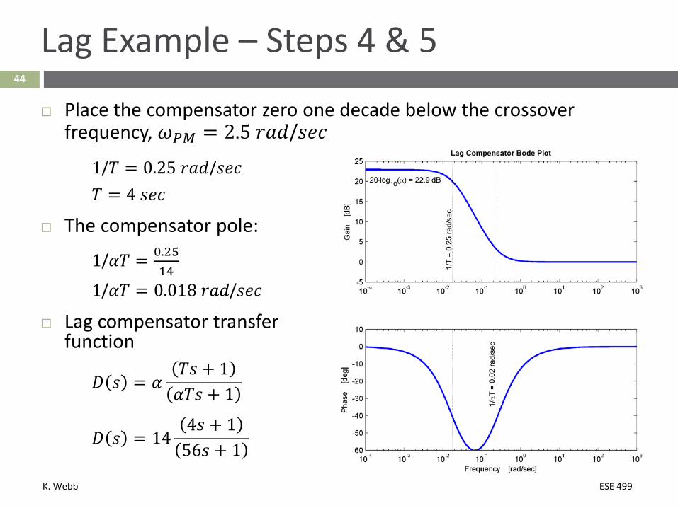
Lag Example – Steps 4 & 5
Place the compensator zero one decade below the crossover frequency, 𝑗𝑗𝑃𝑃𝑃𝑃 = 2.5 𝑟𝑟𝑟𝑟𝑑𝑑/𝑠𝑠𝑑𝑑𝑑𝑑
1/𝑇𝑇 = 0.25 𝑟𝑟𝑟𝑟𝑑𝑑/𝑠𝑠𝑑𝑑𝑑𝑑𝑇𝑇 = 4 𝑠𝑠𝑑𝑑𝑑𝑑
The compensator pole:
1/𝛼𝛼𝑇𝑇 = 0.2514
1/𝛼𝛼𝑇𝑇 = 0.018 𝑟𝑟𝑟𝑟𝑑𝑑/𝑠𝑠𝑑𝑑𝑑𝑑
Lag compensator transfer function
𝐷𝐷 𝑠𝑠 = 𝛼𝛼𝑇𝑇𝑠𝑠 + 1𝛼𝛼𝑇𝑇𝑠𝑠 + 1
𝐷𝐷 𝑠𝑠 = 144𝑠𝑠 + 156𝑠𝑠 + 1
K. Webb ESE 499
45
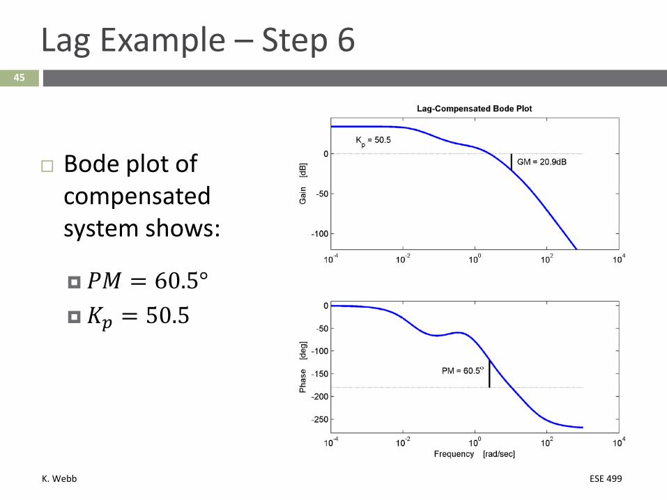
Lag Example – Step 6
Bode plot of compensated system shows:
𝑃𝑃𝑃𝑃 = 60.5°𝐾𝐾𝑝𝑝 = 50.5
K. Webb ESE 499
46
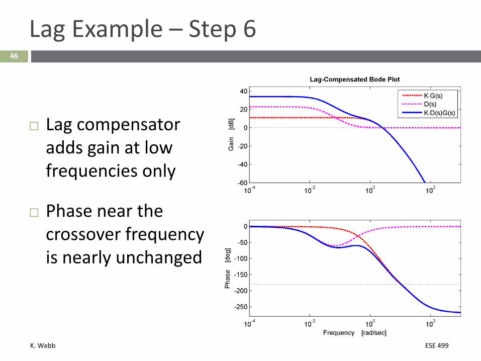
Lag Example – Step 6
Lag compensator adds gain at low frequencies only
Phase near the crossover frequency is nearly unchanged
K. Webb ESE 499
47
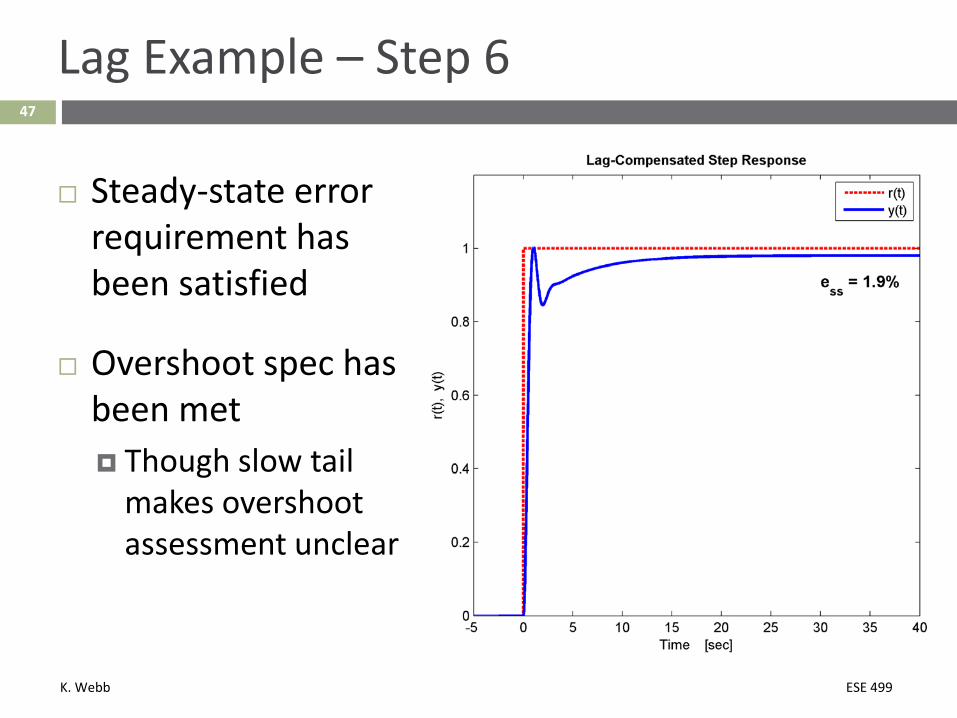
Lag Example – Step 6
Steady-state error requirement has been satisfied
Overshoot spec has been met Though slow tail
makes overshoot assessment unclear
K. Webb ESE 499
48
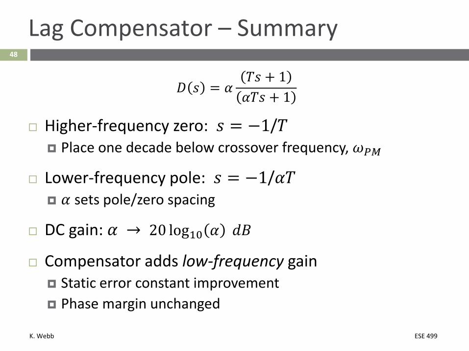
Lag Compensator – Summary
𝐷𝐷 𝑠𝑠 = 𝛼𝛼𝑇𝑇𝑠𝑠 + 1𝛼𝛼𝑇𝑇𝑠𝑠 + 1
Higher-frequency zero: 𝑠𝑠 = −1/𝑇𝑇 Place one decade below crossover frequency, 𝑗𝑗𝑃𝑃𝑃𝑃
Lower-frequency pole: 𝑠𝑠 = −1/𝛼𝛼𝑇𝑇 𝛼𝛼 sets pole/zero spacing
DC gain: 𝛼𝛼 → 20 log10 𝛼𝛼 𝑑𝑑𝑑𝑑
Compensator adds low-frequency gain Static error constant improvement Phase margin unchanged
K. Webb ESE 499
Improving Dynamic Response49
K. Webb ESE 499
50
Improving Dynamic Response
We’ve already seen two types of compensators to improve dynamic response Proportional derivative (PD) compensation Lead compensation
Unlike with the lag compensator we just looked at, here, the objective is to alter the open-loop phase
We’ll look briefly at PD compensation, but will focus on lead compensation
K. Webb ESE 499
Derivative Compensation51
K. Webb ESE 499
52
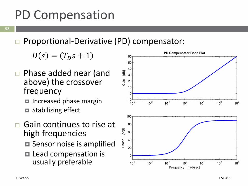
PD Compensation
Proportional-Derivative (PD) compensator:𝐷𝐷 𝑠𝑠 = 𝑇𝑇𝐷𝐷𝑠𝑠 + 1
Phase added near (and above) the crossover frequency Increased phase margin Stabilizing effect
Gain continues to rise at high frequencies Sensor noise is amplified Lead compensation is
usually preferable
K. Webb ESE 499
Lead Compensation53
K. Webb ESE 499
54
Lead Compensation
With lead compensation, we have three design parameters: Crossover frequency, 𝑗𝑗𝑃𝑃𝑃𝑃 Determines closed-loop bandwidth, 𝑗𝑗𝐵𝐵𝐵𝐵; risetime, 𝑡𝑡𝑟𝑟; peak time, 𝑡𝑡𝑝𝑝; and settling time, 𝑡𝑡𝑠𝑠
Phase margin, PM Determines damping, 𝜁𝜁, and overshoot
Low-frequency gain Determines steady-state error performance
We’ll look at the design of lead compensators for two common scenarios, either Designing for steady-state error and phase margin, or Designing for closed-loop bandwidth and phase margin
K. Webb ESE 499
55
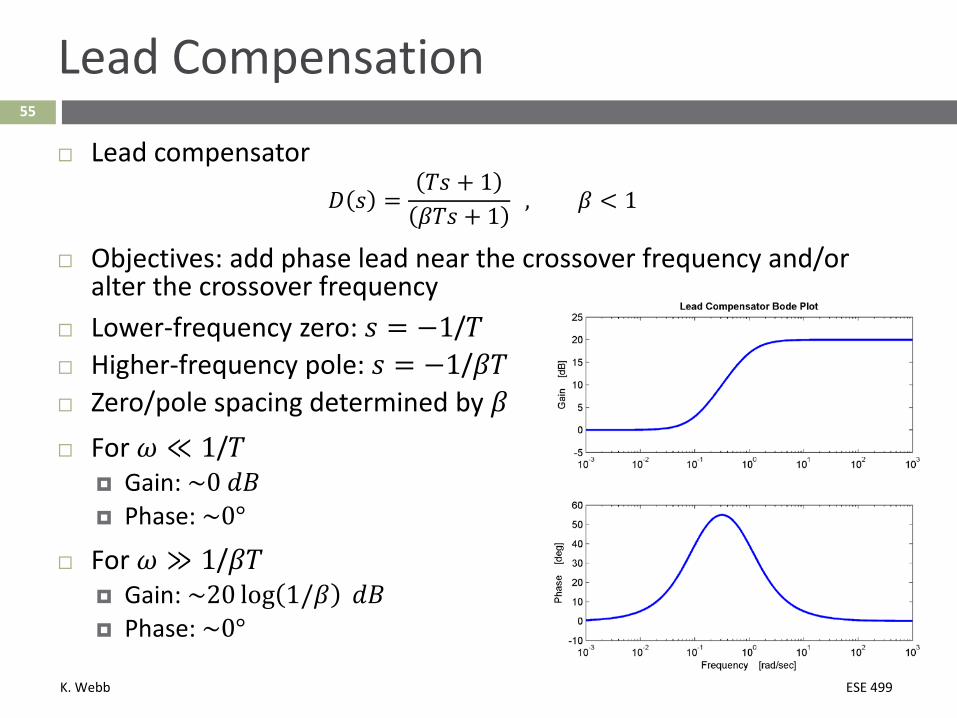
Lead Compensation
Lead compensator
𝐷𝐷 𝑠𝑠 =𝑇𝑇𝑠𝑠 + 1𝛽𝛽𝑇𝑇𝑠𝑠 + 1
, 𝛽𝛽 < 1
Objectives: add phase lead near the crossover frequency and/or alter the crossover frequency
Lower-frequency zero: 𝑠𝑠 = −1/𝑇𝑇 Higher-frequency pole: 𝑠𝑠 = −1/𝛽𝛽𝑇𝑇 Zero/pole spacing determined by 𝛽𝛽 For 𝑗𝑗 ≪ 1/𝑇𝑇
Gain: ~0 𝑑𝑑𝑑𝑑 Phase: ~0°
For 𝑗𝑗 ≫ 1/𝛽𝛽𝑇𝑇 Gain: ~20 log 1/𝛽𝛽 𝑑𝑑𝑑𝑑 Phase: ~0°
K. Webb ESE 499
56
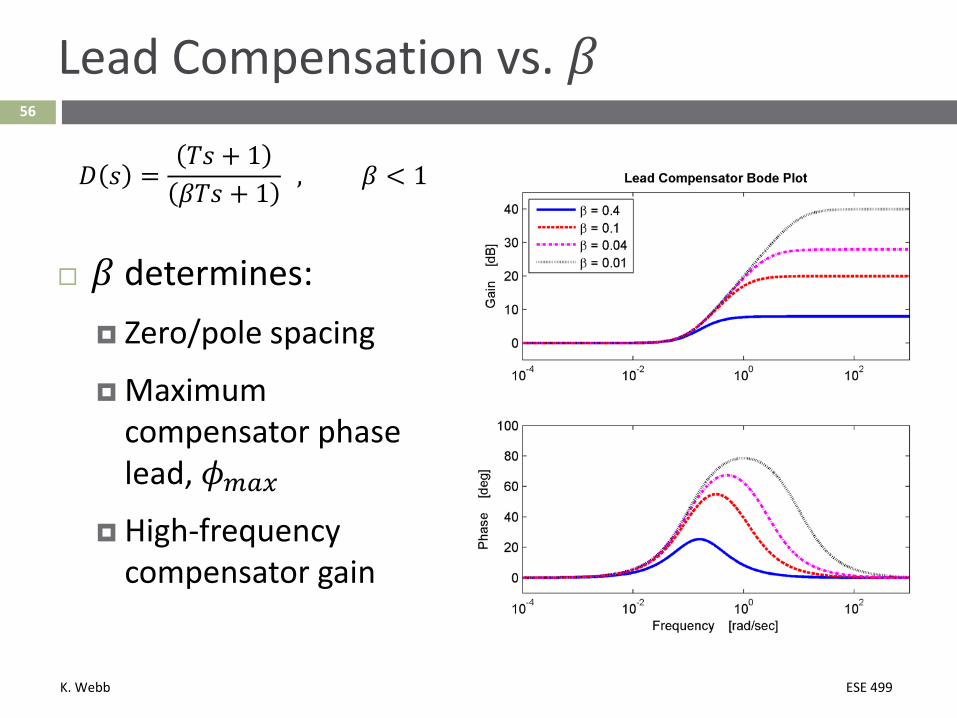
Lead Compensation vs. 𝛽𝛽
𝐷𝐷 𝑠𝑠 =𝑇𝑇𝑠𝑠 + 1𝛽𝛽𝑇𝑇𝑠𝑠 + 1
, 𝛽𝛽 < 1
𝛽𝛽 determines: Zero/pole spacing
Maximum compensator phase lead, 𝜙𝜙𝑚𝑚𝑎𝑎𝑚𝑚
High-frequency compensator gain
K. Webb ESE 499
57
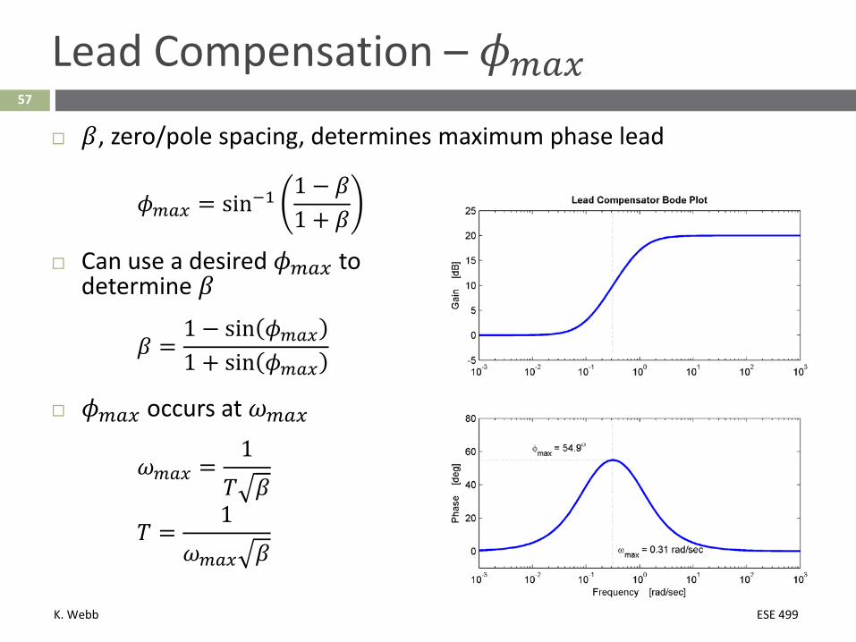
Lead Compensation – 𝜙𝜙𝑚𝑚𝑎𝑎𝑚𝑚 𝛽𝛽, zero/pole spacing, determines maximum phase lead
𝜙𝜙𝑚𝑚𝑎𝑎𝑚𝑚 = sin−11 − 𝛽𝛽1 + 𝛽𝛽
Can use a desired 𝜙𝜙𝑚𝑚𝑎𝑎𝑚𝑚 to determine 𝛽𝛽
𝛽𝛽 =1 − sin 𝜙𝜙𝑚𝑚𝑎𝑎𝑚𝑚1 + sin 𝜙𝜙𝑚𝑚𝑎𝑎𝑚𝑚
𝜙𝜙𝑚𝑚𝑎𝑎𝑚𝑚 occurs at 𝑗𝑗𝑚𝑚𝑎𝑎𝑚𝑚
𝑗𝑗𝑚𝑚𝑎𝑎𝑚𝑚 =1
𝑇𝑇 𝛽𝛽
𝑇𝑇 =1
𝑗𝑗𝑚𝑚𝑎𝑎𝑚𝑚 𝛽𝛽
K. Webb ESE 499
58
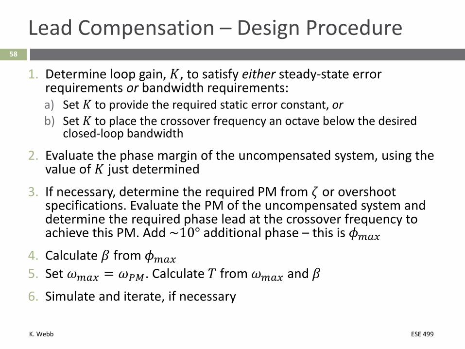
Lead Compensation – Design Procedure
1. Determine loop gain, 𝐾𝐾, to satisfy either steady-state error requirements or bandwidth requirements:a) Set 𝐾𝐾 to provide the required static error constant, orb) Set 𝐾𝐾 to place the crossover frequency an octave below the desired
closed-loop bandwidth
2. Evaluate the phase margin of the uncompensated system, using the value of 𝐾𝐾 just determined
3. If necessary, determine the required PM from 𝜁𝜁 or overshoot specifications. Evaluate the PM of the uncompensated system and determine the required phase lead at the crossover frequency to achieve this PM. Add ~10° additional phase – this is 𝜙𝜙𝑚𝑚𝑎𝑎𝑚𝑚
4. Calculate 𝛽𝛽 from 𝜙𝜙𝑚𝑚𝑎𝑎𝑚𝑚5. Set 𝑗𝑗𝑚𝑚𝑎𝑎𝑚𝑚 = 𝑗𝑗𝑃𝑃𝑃𝑃. Calculate 𝑇𝑇 from 𝑗𝑗𝑚𝑚𝑎𝑎𝑚𝑚 and 𝛽𝛽6. Simulate and iterate, if necessary
K. Webb ESE 499
59
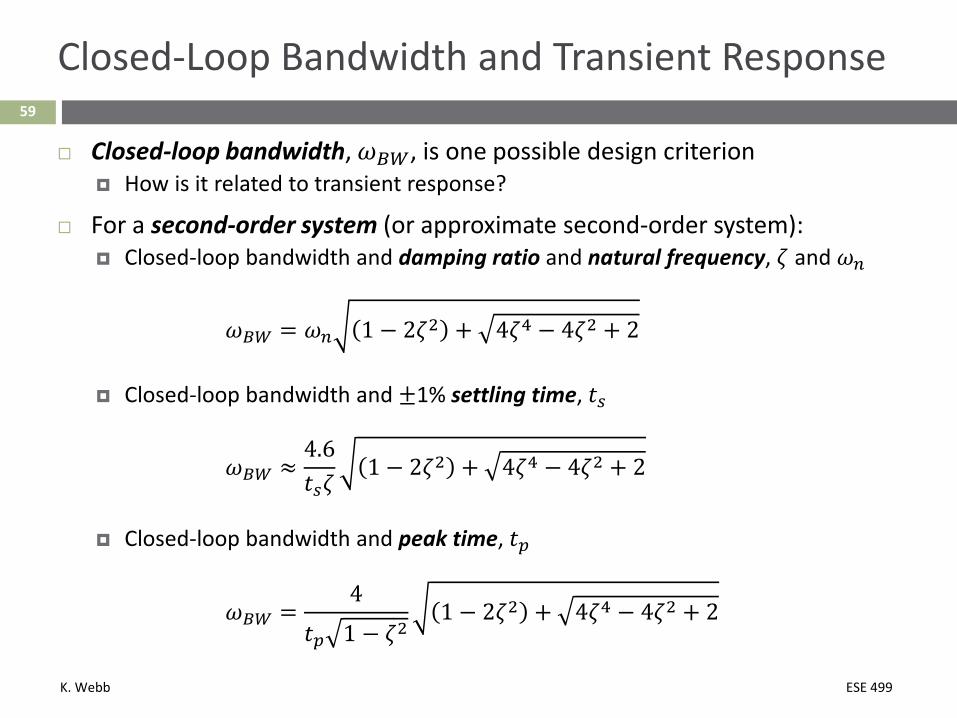
Closed-Loop Bandwidth and Transient Response
Closed-loop bandwidth, 𝑗𝑗𝐵𝐵𝐵𝐵, is one possible design criterion How is it related to transient response?
For a second-order system (or approximate second-order system): Closed-loop bandwidth and damping ratio and natural frequency, 𝜁𝜁 and 𝑗𝑗𝑛𝑛
𝑗𝑗𝐵𝐵𝐵𝐵 = 𝑗𝑗𝑛𝑛 1 − 2𝜁𝜁2 + 4𝜁𝜁4 − 4𝜁𝜁2 + 2
Closed-loop bandwidth and ±1% settling time, 𝑡𝑡𝑠𝑠
𝑗𝑗𝐵𝐵𝐵𝐵 ≈4.6𝑡𝑡𝑠𝑠𝜁𝜁
1 − 2𝜁𝜁2 + 4𝜁𝜁4 − 4𝜁𝜁2 + 2
Closed-loop bandwidth and peak time, 𝑡𝑡𝑝𝑝
𝑗𝑗𝐵𝐵𝐵𝐵 =4
𝑡𝑡𝑝𝑝 1 − 𝜁𝜁21 − 2𝜁𝜁2 + 4𝜁𝜁4 − 4𝜁𝜁2 + 2
K. Webb ESE 499
60
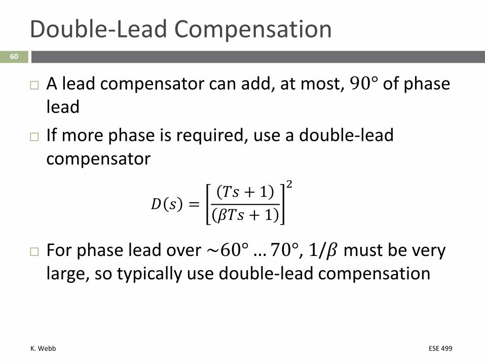
Double-Lead Compensation
A lead compensator can add, at most, 90° of phase lead
If more phase is required, use a double-lead compensator
𝐷𝐷 𝑠𝑠 =𝑇𝑇𝑠𝑠 + 1𝛽𝛽𝑇𝑇𝑠𝑠 + 1
2
For phase lead over ~60° … 70°, 1/𝛽𝛽 must be very large, so typically use double-lead compensation
K. Webb ESE 499
61
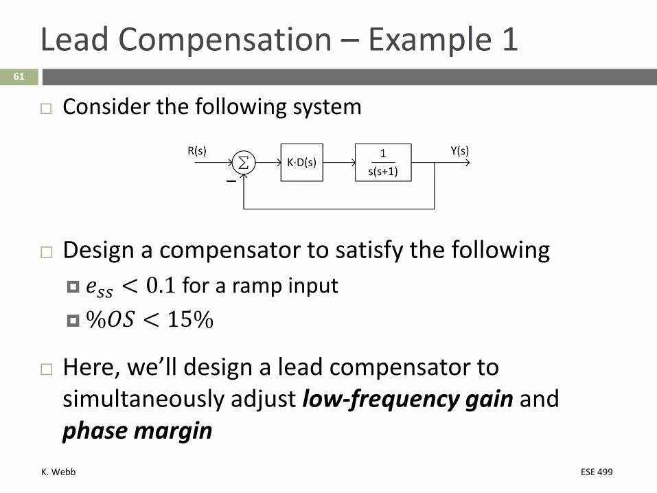
Lead Compensation – Example 1
Consider the following system
Design a compensator to satisfy the following 𝑑𝑑𝑠𝑠𝑠𝑠 < 0.1 for a ramp input%𝑂𝑂𝑂𝑂 < 15%
Here, we’ll design a lead compensator to simultaneously adjust low-frequency gain and phase margin
K. Webb ESE 499
62
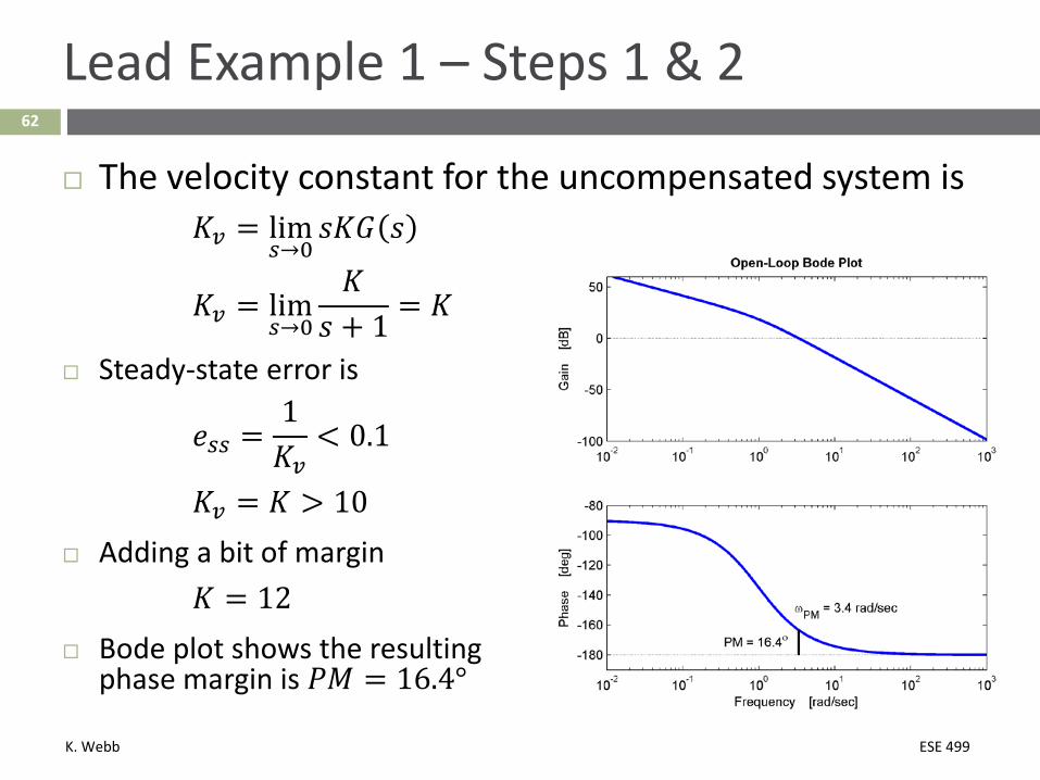
Lead Example 1 – Steps 1 & 2
The velocity constant for the uncompensated system is𝐾𝐾𝑣𝑣 = lim
𝑠𝑠→0𝑠𝑠𝐾𝐾𝐺𝐺 𝑠𝑠
𝐾𝐾𝑣𝑣 = lim𝑠𝑠→0
𝐾𝐾𝑠𝑠 + 1 = 𝐾𝐾
Steady-state error is
𝑑𝑑𝑠𝑠𝑠𝑠 =1𝐾𝐾𝑣𝑣
< 0.1
𝐾𝐾𝑣𝑣 = 𝐾𝐾 > 10 Adding a bit of margin
𝐾𝐾 = 12 Bode plot shows the resulting
phase margin is 𝑃𝑃𝑃𝑃 = 16.4°
K. Webb ESE 499
63
Lead Example 1 – Step 3
Approximate required phase margin for %𝑂𝑂𝑂𝑂 < 15% Design for 13%
First calculate the required damping ratio
𝜁𝜁 = −ln 𝑂𝑂𝑂𝑂
𝜋𝜋2 + ln2 𝑂𝑂𝑂𝑂= 0.545
Approximate corresponding PM, and add 10° correction factor
𝑃𝑃𝑃𝑃 ≈ 100𝜁𝜁 + 10° = 64.5°
Calculate the required phase lead
𝜙𝜙𝑚𝑚𝑎𝑎𝑚𝑚 = 64.5° − 16.4° = 48°
K. Webb ESE 499
64
Lead Example 1 – Steps 4 & 5
Calculate 𝛽𝛽 from 𝜙𝜙𝑚𝑚𝑎𝑎𝑚𝑚
𝛽𝛽 =1 − sin 𝜙𝜙𝑚𝑚𝑎𝑎𝑚𝑚1 + sin 𝜙𝜙𝑚𝑚𝑎𝑎𝑚𝑚
= 0.147
Set 𝑗𝑗𝑚𝑚𝑎𝑎𝑚𝑚 = 𝑗𝑗𝑃𝑃𝑃𝑃, as determined from Bode plot, and calculate 𝑇𝑇
𝑗𝑗𝑚𝑚𝑎𝑎𝑚𝑚 = 𝑗𝑗𝑃𝑃𝑃𝑃 = 3.4 𝑟𝑟𝑟𝑟𝑑𝑑/𝑠𝑠𝑑𝑑𝑑𝑑
𝑇𝑇 = 1𝜔𝜔𝑚𝑚𝑎𝑎𝑚𝑚 𝛽𝛽
= 13.4 0.147
= 0.766
The resulting lead compensator transfer function is
𝐾𝐾𝐷𝐷 𝑠𝑠 = 𝐾𝐾𝑇𝑇𝑠𝑠 + 1𝛽𝛽𝑇𝑇𝑠𝑠 + 1
= 120.766𝑠𝑠 + 10.113𝑠𝑠 + 1
K. Webb ESE 499
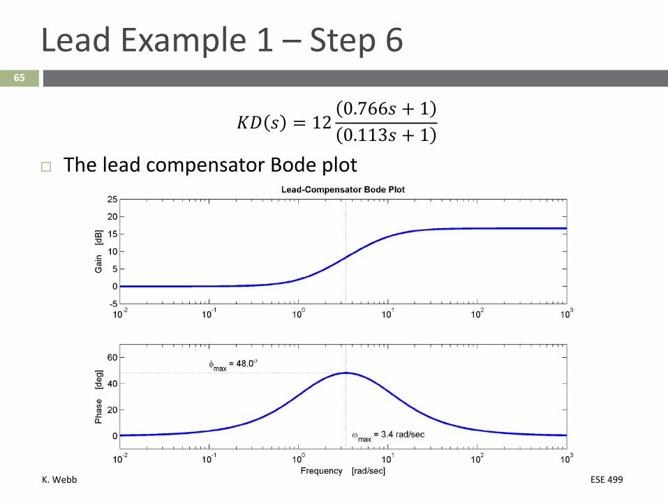
65
Lead Example 1 – Step 6
𝐾𝐾𝐷𝐷 𝑠𝑠 = 120.766𝑠𝑠 + 10.113𝑠𝑠 + 1
The lead compensator Bode plot
K. Webb ESE 499
66
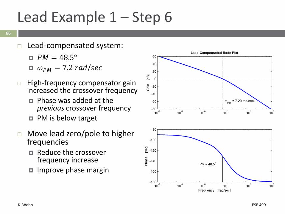
Lead Example 1 – Step 6
Lead-compensated system: 𝑃𝑃𝑃𝑃 = 48.5° 𝑗𝑗𝑃𝑃𝑃𝑃 = 7.2 𝑟𝑟𝑟𝑟𝑑𝑑/𝑠𝑠𝑑𝑑𝑑𝑑
High-frequency compensator gain increased the crossover frequency Phase was added at the
previous crossover frequency PM is below target
Move lead zero/pole to higher frequencies Reduce the crossover
frequency increase Improve phase margin
K. Webb ESE 499
67
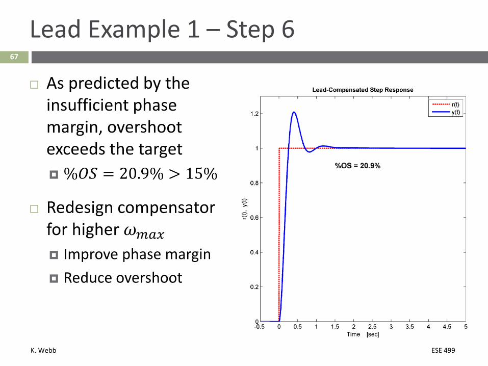
Lead Example 1 – Step 6
As predicted by the insufficient phase margin, overshoot exceeds the target %𝑂𝑂𝑂𝑂 = 20.9% > 15%
Redesign compensator for higher 𝑗𝑗𝑚𝑚𝑎𝑎𝑚𝑚 Improve phase margin Reduce overshoot
K. Webb ESE 499
68
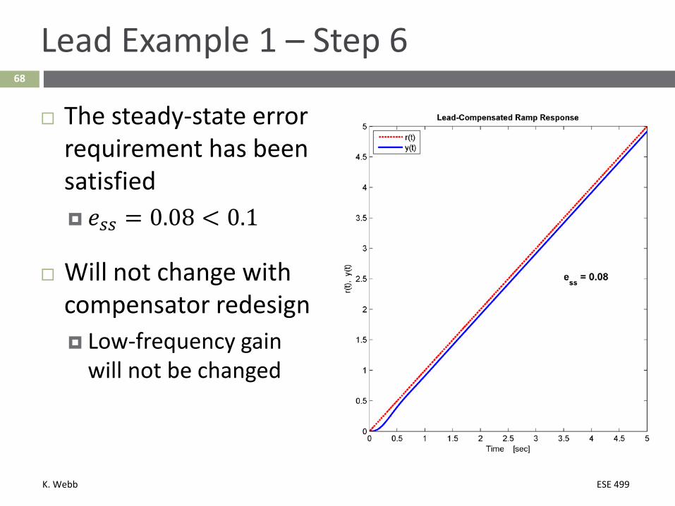
Lead Example 1 – Step 6
The steady-state error requirement has been satisfied 𝑑𝑑𝑠𝑠𝑠𝑠 = 0.08 < 0.1
Will not change with compensator redesign Low-frequency gain
will not be changed
K. Webb ESE 499
69
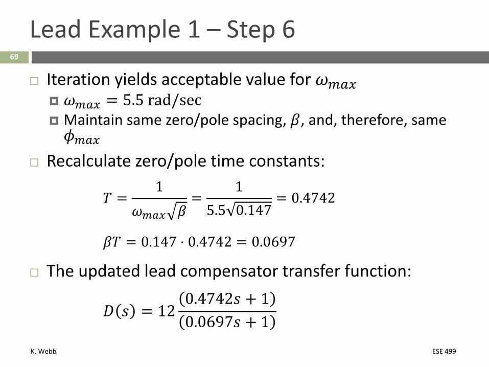
Lead Example 1 – Step 6
Iteration yields acceptable value for 𝑗𝑗𝑚𝑚𝑎𝑎𝑚𝑚 𝑗𝑗𝑚𝑚𝑎𝑎𝑚𝑚 = 5.5 rad/sec Maintain same zero/pole spacing, 𝛽𝛽, and, therefore, same 𝜙𝜙𝑚𝑚𝑎𝑎𝑚𝑚
Recalculate zero/pole time constants:
𝑇𝑇 =1
𝑗𝑗𝑚𝑚𝑎𝑎𝑚𝑚 𝛽𝛽=
15.5 0.147
= 0.4742
𝛽𝛽𝑇𝑇 = 0.147 ⋅ 0.4742 = 0.0697
The updated lead compensator transfer function:
𝐷𝐷 𝑠𝑠 = 120.4742𝑠𝑠 + 10.0697𝑠𝑠 + 1
K. Webb ESE 499
70
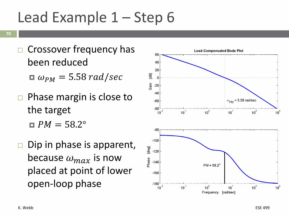
Lead Example 1 – Step 6
Crossover frequency has been reduced 𝑗𝑗𝑃𝑃𝑃𝑃 = 5.58 𝑟𝑟𝑟𝑟𝑑𝑑/𝑠𝑠𝑑𝑑𝑑𝑑
Phase margin is close to the target 𝑃𝑃𝑃𝑃 = 58.2°
Dip in phase is apparent, because 𝑗𝑗𝑚𝑚𝑎𝑎𝑚𝑚 is now placed at point of lower open-loop phase
K. Webb ESE 499
71
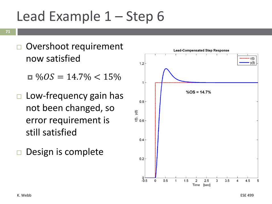
Lead Example 1 – Step 6
Overshoot requirement now satisfied
%𝑂𝑂𝑂𝑂 = 14.7% < 15%
Low-frequency gain has not been changed, so error requirement is still satisfied
Design is complete
K. Webb ESE 499
72
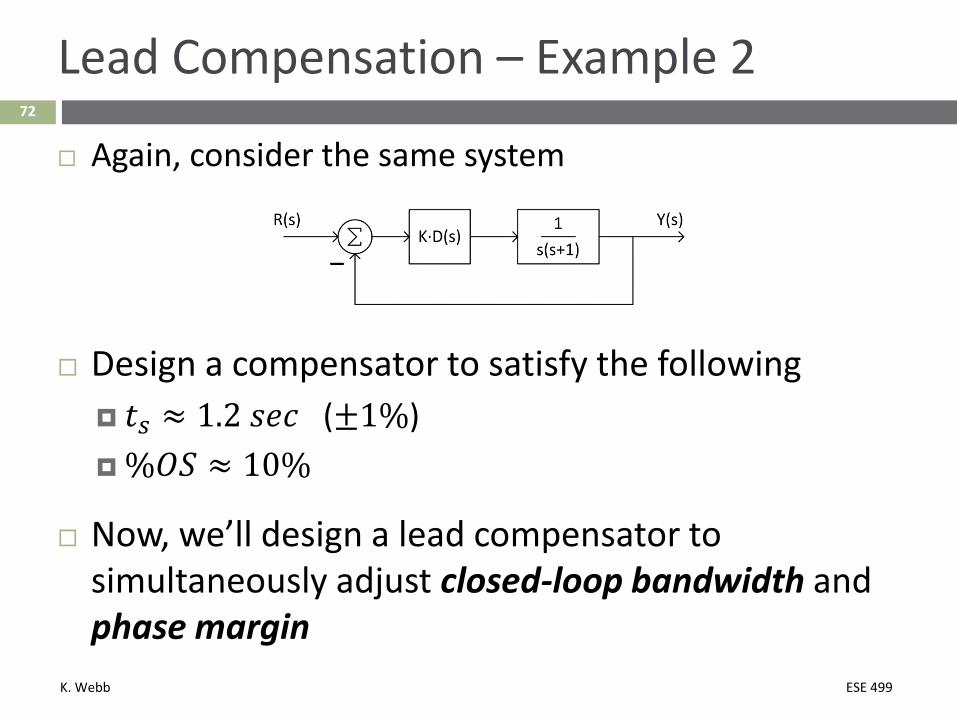
Lead Compensation – Example 2
Again, consider the same system
Design a compensator to satisfy the following 𝑡𝑡𝑠𝑠 ≈ 1.2 𝑠𝑠𝑑𝑑𝑑𝑑 (±1%)%𝑂𝑂𝑂𝑂 ≈ 10%
Now, we’ll design a lead compensator to simultaneously adjust closed-loop bandwidth and phase margin
K. Webb ESE 499
73
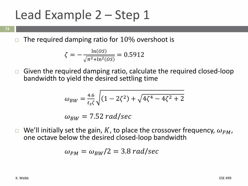
Lead Example 2 – Step 1
The required damping ratio for 10% overshoot is
𝜁𝜁 = − ln 𝑂𝑂𝑂𝑂𝜋𝜋2+ln2 𝑂𝑂𝑂𝑂
= 0.5912
Given the required damping ratio, calculate the required closed-loop bandwidth to yield the desired settling time
𝑗𝑗𝐵𝐵𝐵𝐵 = 4.6𝑡𝑡𝑠𝑠𝜁𝜁
1 − 2𝜁𝜁2 + 4𝜁𝜁4 − 4𝜁𝜁2 + 2
𝑗𝑗𝐵𝐵𝐵𝐵 = 7.52 𝑟𝑟𝑟𝑟𝑑𝑑/𝑠𝑠𝑑𝑑𝑑𝑑
We’ll initially set the gain, 𝐾𝐾, to place the crossover frequency, 𝑗𝑗𝑃𝑃𝑃𝑃, one octave below the desired closed-loop bandwidth
𝑗𝑗𝑃𝑃𝑃𝑃 = 𝑗𝑗𝐵𝐵𝐵𝐵/2 = 3.8 𝑟𝑟𝑟𝑟𝑑𝑑/𝑠𝑠𝑑𝑑𝑑𝑑
K. Webb ESE 499
74
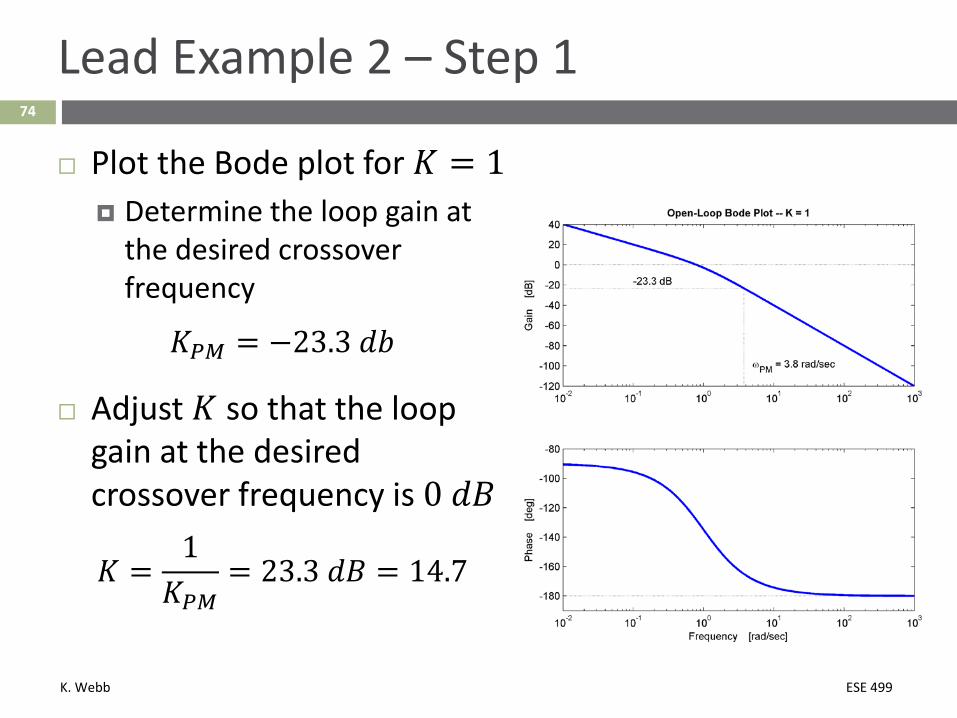
Lead Example 2 – Step 1
Plot the Bode plot for 𝐾𝐾 = 1 Determine the loop gain at
the desired crossover frequency
𝐾𝐾𝑃𝑃𝑃𝑃 = −23.3 𝑑𝑑𝑑𝑑
Adjust 𝐾𝐾 so that the loop gain at the desired crossover frequency is 0 𝑑𝑑𝑑𝑑
𝐾𝐾 =1𝐾𝐾𝑃𝑃𝑃𝑃
= 23.3 𝑑𝑑𝑑𝑑 = 14.7
K. Webb ESE 499
75
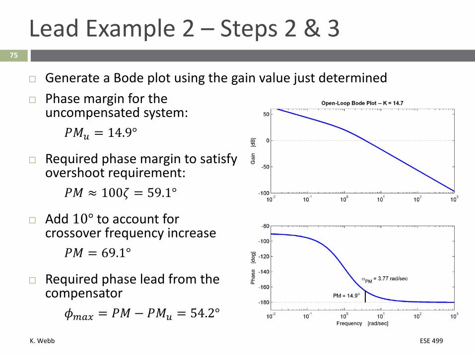
Lead Example 2 – Steps 2 & 3
Phase margin for the uncompensated system:
𝑃𝑃𝑃𝑃𝑝𝑝 = 14.9°
Required phase margin to satisfy overshoot requirement:
𝑃𝑃𝑃𝑃 ≈ 100𝜁𝜁 = 59.1°
Add 10° to account for crossover frequency increase
𝑃𝑃𝑃𝑃 = 69.1°
Required phase lead from the compensator
𝜙𝜙𝑚𝑚𝑎𝑎𝑚𝑚 = 𝑃𝑃𝑃𝑃 − 𝑃𝑃𝑃𝑃𝑝𝑝 = 54.2°
Generate a Bode plot using the gain value just determined
K. Webb ESE 499
76
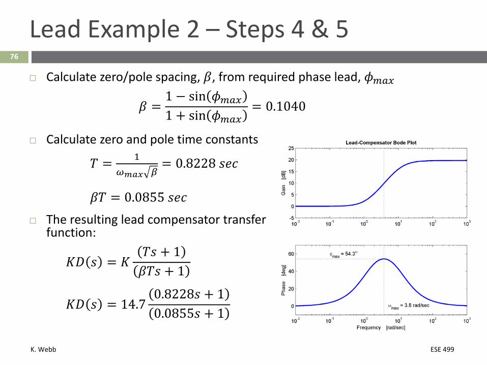
Lead Example 2 – Steps 4 & 5
Calculate zero/pole spacing, 𝛽𝛽, from required phase lead, 𝜙𝜙𝑚𝑚𝑎𝑎𝑚𝑚
𝛽𝛽 =1 − sin 𝜙𝜙𝑚𝑚𝑎𝑎𝑚𝑚1 + sin 𝜙𝜙𝑚𝑚𝑎𝑎𝑚𝑚
= 0.1040
Calculate zero and pole time constants
𝑇𝑇 = 1𝜔𝜔𝑚𝑚𝑎𝑎𝑚𝑚 𝛽𝛽
= 0.8228 𝑠𝑠𝑑𝑑𝑑𝑑
𝛽𝛽𝑇𝑇 = 0.0855 𝑠𝑠𝑑𝑑𝑑𝑑 The resulting lead compensator transfer
function:
𝐾𝐾𝐷𝐷 𝑠𝑠 = 𝐾𝐾𝑇𝑇𝑠𝑠 + 1𝛽𝛽𝑇𝑇𝑠𝑠 + 1
𝐾𝐾𝐷𝐷 𝑠𝑠 = 14.70.8228𝑠𝑠 + 10.0855𝑠𝑠 + 1
K. Webb ESE 499
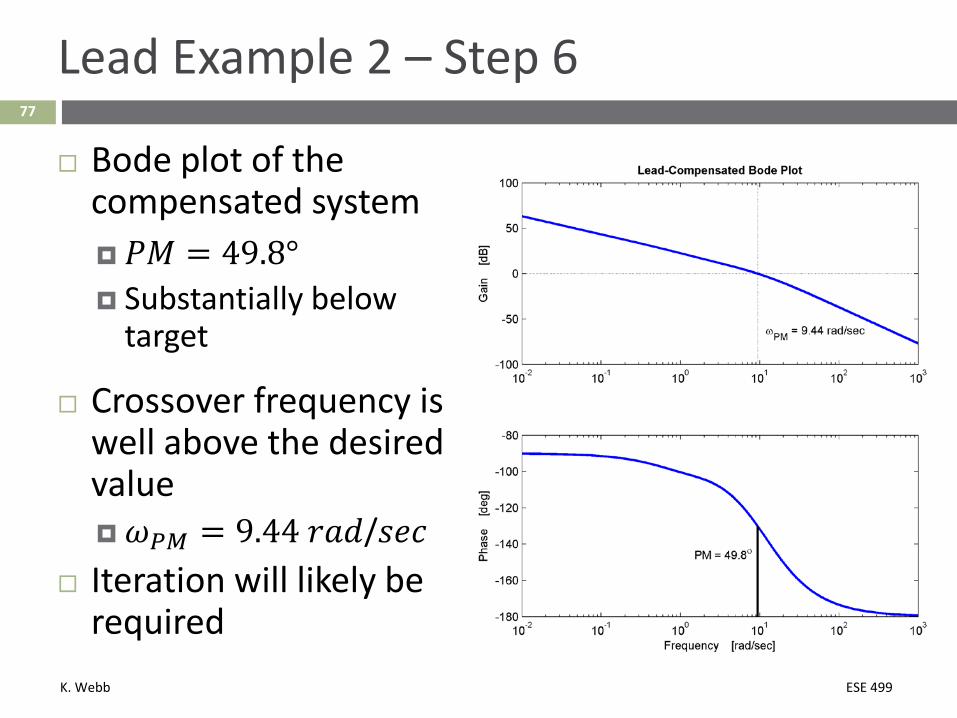
77
Lead Example 2 – Step 6
Bode plot of the compensated system 𝑃𝑃𝑃𝑃 = 49.8° Substantially below
target
Crossover frequency is well above the desired value𝑗𝑗𝑃𝑃𝑃𝑃 = 9.44 𝑟𝑟𝑟𝑟𝑑𝑑/𝑠𝑠𝑑𝑑𝑑𝑑
Iteration will likely be required
K. Webb ESE 499
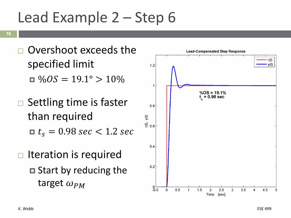
78
Lead Example 2 – Step 6
Overshoot exceeds the specified limit %𝑂𝑂𝑂𝑂 = 19.1° > 10%
Settling time is faster than required 𝑡𝑡𝑠𝑠 = 0.98 𝑠𝑠𝑑𝑑𝑑𝑑 < 1.2 𝑠𝑠𝑑𝑑𝑑𝑑
Iteration is required Start by reducing the
target 𝑗𝑗𝑃𝑃𝑃𝑃
K. Webb ESE 499
79
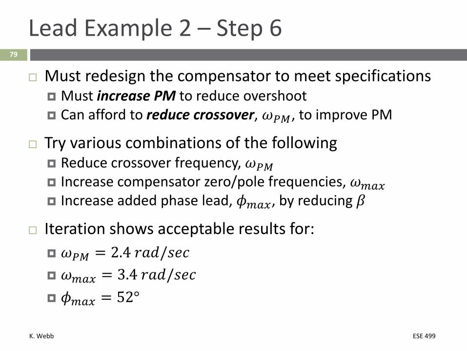
Lead Example 2 – Step 6
Must redesign the compensator to meet specifications Must increase PM to reduce overshoot Can afford to reduce crossover, 𝑗𝑗𝑃𝑃𝑃𝑃, to improve PM
Try various combinations of the following Reduce crossover frequency, 𝑗𝑗𝑃𝑃𝑃𝑃 Increase compensator zero/pole frequencies, 𝑗𝑗𝑚𝑚𝑎𝑎𝑚𝑚 Increase added phase lead, 𝜙𝜙𝑚𝑚𝑎𝑎𝑚𝑚, by reducing 𝛽𝛽
Iteration shows acceptable results for: 𝑗𝑗𝑃𝑃𝑃𝑃 = 2.4 𝑟𝑟𝑟𝑟𝑑𝑑/𝑠𝑠𝑑𝑑𝑑𝑑 𝑗𝑗𝑚𝑚𝑎𝑎𝑚𝑚 = 3.4 𝑟𝑟𝑟𝑟𝑑𝑑/𝑠𝑠𝑑𝑑𝑑𝑑 𝜙𝜙𝑚𝑚𝑎𝑎𝑚𝑚 = 52°
K. Webb ESE 499
80
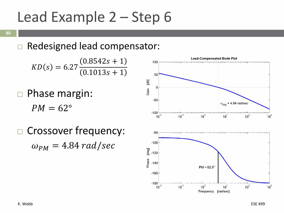
Lead Example 2 – Step 6
Redesigned lead compensator:
𝐾𝐾𝐷𝐷 𝑠𝑠 = 6.270.8542𝑠𝑠 + 10.1013𝑠𝑠 + 1
Phase margin:𝑃𝑃𝑃𝑃 = 62°
Crossover frequency:𝑗𝑗𝑃𝑃𝑃𝑃 = 4.84 𝑟𝑟𝑟𝑟𝑑𝑑/𝑠𝑠𝑑𝑑𝑑𝑑
K. Webb ESE 499
81
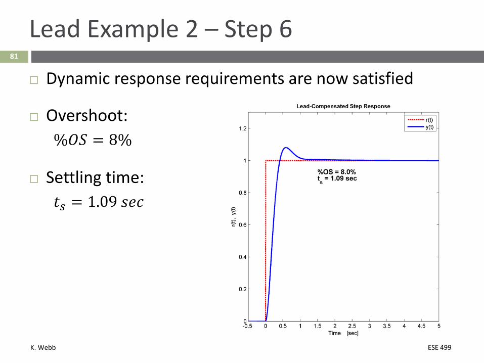
Lead Example 2 – Step 6
Dynamic response requirements are now satisfied
Overshoot:%𝑂𝑂𝑂𝑂 = 8%
Settling time:𝑡𝑡𝑠𝑠 = 1.09 𝑠𝑠𝑑𝑑𝑑𝑑
K. Webb ESE 499
82
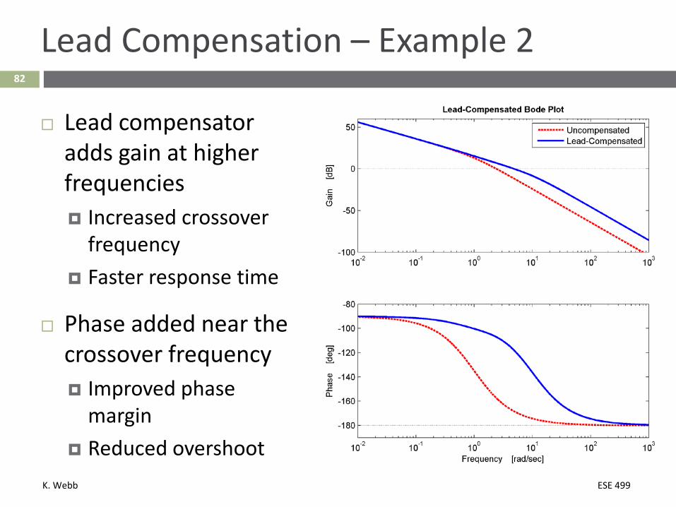
Lead Compensation – Example 2
Lead compensator adds gain at higher frequencies Increased crossover
frequency Faster response time
Phase added near the crossover frequency Improved phase
margin Reduced overshoot
K. Webb ESE 499
83
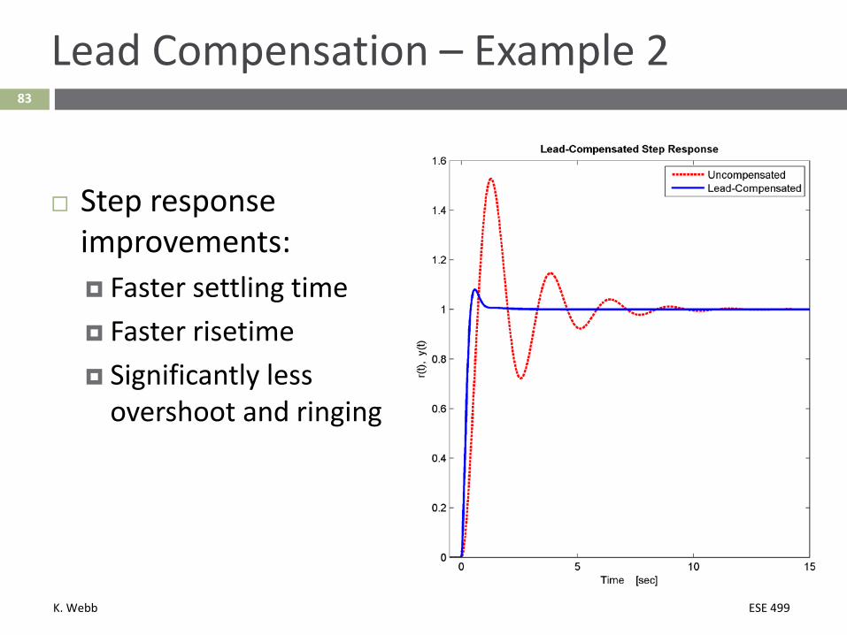
Lead Compensation – Example 2
Step response improvements: Faster settling time Faster risetime Significantly less
overshoot and ringing
K. Webb ESE 499
84
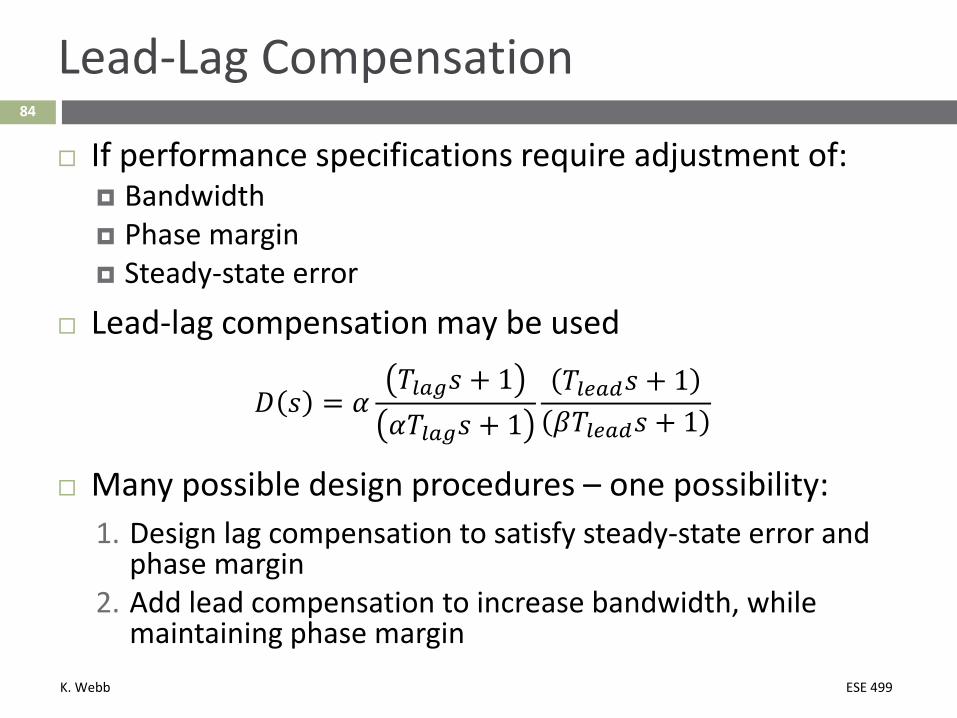
Lead-Lag Compensation
If performance specifications require adjustment of: Bandwidth Phase margin Steady-state error
Lead-lag compensation may be used
𝐷𝐷 𝑠𝑠 = 𝛼𝛼𝑇𝑇𝑙𝑙𝑎𝑎𝑙𝑙𝑠𝑠 + 1𝛼𝛼𝑇𝑇𝑙𝑙𝑎𝑎𝑙𝑙𝑠𝑠 + 1
𝑇𝑇𝑙𝑙𝑙𝑙𝑎𝑎𝑙𝑙𝑠𝑠 + 1𝛽𝛽𝑇𝑇𝑙𝑙𝑙𝑙𝑎𝑎𝑙𝑙𝑠𝑠 + 1
Many possible design procedures – one possibility:1. Design lag compensation to satisfy steady-state error and
phase margin2. Add lead compensation to increase bandwidth, while
maintaining phase margin