Embed Size (px)
DESCRIPTION
ups
Citation preview

Section 8: ‘1+1’ UPS System Control
Chapter 1 - "1+1" Configured Systems
1.1 Introduction .............................................................................................. 8-11.1.1 “1+1” Power circuit considerations ............................................. 8-11.1.2 “1+1” Control circuit considerations ........................................... 8-1
Chapter 2 - Parallel Logic Board – 4520075B
2.1 Chapter Overview. .................................................................................... 8-5
2.2 General Description .................................................................................. 8-52.2.1 Input/Output connections ............................................................. 8-52.2.2 Circuit board functions .............................................................. 8-10
2.3 General module output control ............................................................... 8-122.3.1 Inverter ON/OFF request – [OFF_INV> ........................................ 8-12
Selective shutdown .......................................................... 8-132.3.2 Load transfer control .................................................................. 8-15
Load-on-inverter request – [C_L_INV> .......................... 8-16Load-on-bypass request – [O_BUS_INV_L> ................. 8-17
2.4 Frequency synchronisation principles .................................................... 8-192.4.1 Introduction ................................................................................ 8-19
Inverter frequency control – overview ............................. 8-19Basic GVCO sync principles on module start-up ............ 8-20
2.4.2 GVCO Detailed description of operation .................................. 8-232.4.3 PLL Phase Comparator (D29) ................................................... 8-262.4.4 D30 Parallel Control Functions ................................................. 8-26
Bypass validation ............................................................. 8-27Sync source selector ......................................................... 8-27Sync bus comparator ........................................................ 8-28VCO-in-loop relay control ............................................... 8-28Internal Sync Logic .......................................................... 8-29
2.5 Output current sharing ............................................................................ 8-312.5.1 Introduction ................................................................................ 8-312.5.2 Current sharing error detection principles ................................. 8-312.5.3 Current-sharing relay control (K3/K4) ...................................... 8-332.5.4 Selective shutdown .................................................................... 8-34
Current-sharing error ....................................................... 8-34Reverse Power detector .................................................... 8-35Forward Power detector ................................................... 8-35
2.5.5 On-line module counter ............................................................. 8-35
2.6 Parallel rectifier operation ...................................................................... 8-362.6.1 Rectifier current-sharing control ................................................ 8-362.6.2 Boost charge control .................................................................. 8-372.6.3 Battery test control ..................................................................... 8-37
11pm.fm5 - Issue 2 Dated 21/08/97 i

SECTION 8 - ‘1+1’ UPS System Control 7200 Series UPS Service Manual
2.7 Other Features and functions .................................................................. 8-382.7.1 Ribbon cable connection monitor .............................................. 8-38
2.8 Parallel Logic Board circuit operation during start-up ........................... 8-392.8.1 Initialisation/reset ....................................................................... 8-392.8.2 Inverter run-up and synchronisation .......................................... 8-392.8.3 Connecting to the parallel control bus ....................................... 8-402.8.4 Load transfer to inverter ............................................................. 8-402.8.5 Load retransfer back to bypass .................................................. 8-42
2.9 Test mode of operation: .......................................................................... 8-42
ii 11pm.fm5 - Issue 2 Dated 21/08/97

Section 8: "1+1" Configured Systems
Chapter 1 - "1+1" Configured Systems
1.1 Introduction
A basic description of the principles of a “1+1” configured system is provided insection 1 (see paragraph 1.4 on page 1-7) – the basic block diagram is repeatedin Figure 8-1, below.
Figure 8-1: “1+1” System configuration block diagram
1.1.1 “1+1” Power circuit considerations
As the above diagram shows, in a ‘1+1’ system the power outputs from the twomodules are connected to an external common output busbar from where it isrouted to the critical load equipment using normal distribution methods. There-fore, from a ‘power’ point of view there are no modifications required to thestandard ‘single-module’ UPS.
1.1.2 “1+1” Control circuit considerations
The extra ‘control’ requirements of a ‘1+1’ system over that of a ‘single-module’are quite extensive due to the fact that the UPS output power terminals are con-nected to a common bus. The additional features require an exchange of variouscontrol and status signals, both analogue and digital, to pass between the twomodules. Such signals are connected via the Parallel Logic Boards which are con-nected together by cross-connected ribbon cables which form a ‘Parallel ControlBus’ – (See Figure 8-2).
StaticBypass
INVERTERRECTIFIER
Output(LOAD)Power-Supply
INV (SS)
Maint. Bypass
StaticBypass
INVERTERRECTIFIER
Maint. Bypass
BYP (SS)
INV (SS)
BYP (SS)
RectifierControl Logic
InverterControl Logic
RectifierControl Logic
InverterControl Logic
Inter-Module Parallel Control Logic
Inter-Module Parallel Control Logic Static SwitchControl Logic
Static SwitchControl Logic
11pm-c1.fm5 - Issue 2 Dated 21/08/97 8-1

SECTION 8 - "1+1" Configured Systems 7200 Series UPS Service ManualCHAPTER 1 - "1+1" Configured Systems
Figure 8-2: ‘1+1’ Control Logic
These inter-module control functions fall into the following broad categories:
Balanced output requirements
It is crucial that the modules’ outputs are balanced in order to prevent a circulatingcurrent flowing from one module to the other, as such an event could cause sig-nificant module damage and invalidate the critical load supply. Balanced condi-tions are achieved by ensuring that the inverters are always fully synchronised toeach other and their output voltages are equal. As with the case of the ‘single-module’ it is also necessary to synchronise the inverters to the bypass supply inorder facilitate a no-break load transfer when required.
Transfer control requirements
Once again due to the paralleled nature of the modules’ outputs, it is crucial thatthe load transfer control mechanisms in each module are controlled from acommon point. That is, to prevent equipment damage due to one module transfer-ring its output to bypass whilst the other is ‘on inverter’. A common controlsystem is therefore used which manages the load transfer according whether thesystem is configured as redundant or non-redundant.
Redundant vs Non-Redundant configuration
Redundant system. In a ‘redundant’ system, if one module fails the remainingmodule will remain on-line to maintain the critical load; therefore if a modulegoes faulty its output contactor is tripped to take it off-line but its static bypass isnot activated. The static bypass circuit is only triggered if a fault develops in thesecond module which requires it also to be taken off-line.
In a redundant system the modules are thus sized such that the potential maxi-mum load can be powered by just one of the two modules. Under normal circum-stances both modules are operational and share the load current equally – i.e.under full load conditions both modules operate at 50% of their nominal rating.
ParallelLogicBoard
UPSLogicBoard
��������������������������������
Rect. Logic Bd
Inv. Logic Bd
Static Sw. Drv. Bd
High Voltage I/F Bd
ParallelLogicBoard
UPSLogicBoard
����������������������������������������
Rect. Logic Bd
Inv. Logic Bd
Static Sw. Drv. Bd
High Voltage I/F Bd
X1X7
X2
X3
X2
X3
X1X1
X3
X5
X2
X1
X3
X5
X2
X7
MODULE 1 MODULE 2Parallel
Bus
8-2 11pm-c1.fm5 - Issue 2 Dated 21/08/97

7200 Series UPS Service Manual SECTION 8 - "1+1" Configured SystemsCHAPTER 1 - "1+1" Configured Systems
Non-redundant system. In a ‘non-redundant’ configuration, if one modulefails then both modules are taken off-line (by opening their output contactors) andthe load transferred to the static bypass. The load will not re-transfer to the invert-ers until both inverters are fully operational and fully synchronised etc.
In a non-redundant system each module’s nominal rating must be at least 50% ofthe potential maximum load.
Inter-module power rectifier control
The power rectifier is only affected by the parallel control bus in a “1+1” systemif a ‘common battery’ is used – i.e. if both UPS modules are connected to a singlebattery bank (via separate battery isolators of course). In this type of installationthe power rectifiers in each module are effectively connected in parallel and mustbe controlled such that the battery charge current is shared equally between them.
A ‘common battery’ option kit is available. This contains DCCTs (DC CurrentTransformers) which are fitted to the battery power lines and connected via theparallel control bus to a sharing circuit in the rectifier control block.
See the Options section in the relevant system IOM user manual for full details.
11pm-c1.fm5 - Issue 2 Dated 21/08/97 8-3

SECTION 8 - "1+1" Configured Systems 7200 Series UPS Service ManualCHAPTER 1 - "1+1" Configured Systems
8-4 11pm-c1.fm5 - Issue 2 Dated 21/08/97

Section 8:
Chapter 2 - Parallel Logic Board – 4520075B
2.1 Chapter Overview.
This chapter contains a circuit description of the Parallel Logic Board used acrossthe whole 7200 Series UPS model range when configured to operate as a ‘1+1’system, and should be read in conjunction with circuit diagram SE-4520075-B (4pages). Signal annotations shown on the circuit diagrams are shown in italics inthe following text – e.g. [SYN_INT>.
2.2 General Description
2.2.1 Input/Output connections
Connectors X2 & X3
As mentioned above, connectors X2 & X3 are cross-connected from one moduleto the other – i.e. X2 on one module is connected to X3 on the other, and vice-versa. The signals passing between these connectors are therefore bi-directional.
Table 8-1:
Pin Signal Signal Function
12
A_CON / 0VB_CON / 0V
Used to detect that the ribbon cable is connected – (See paragraph 2.7.1)
3 B_BLK_SW
If a module applies an [O_BLK_SW> signal to X1-43 it is passed to both modules via this line, and thereby turns off the inverters in both modules by driving the [OFF_INV> output at D31-19 high. (see page 8-12)
4 B_MNS_L_SS
If a module applies an [O_MNS_L_SS> signal to X1-44 it is passed to both modules via this line. This is used by the load transfer control logic when the board is fitted in a multi-module MSS cabinet only, and is overridden in a 1+1 system by jumper X6-4(see page 8-16).
5 B_MNS_D_SS
If a module applies an [O_MNS_D_SS> signal to X1 pin 45 it inhibits the passage of the mains frequency signal [F-IN> through D31 (See paragraph 2.4.4.1). This signal is coupled to the second module via the parallel bus X2/X3 pin 5 (inhibit = low).
6 B_PAR_SYN
This is taken high when the VCO-in-loop relay (K1) is closed in either module, and is used to inform the GVCO whether to start in the “master” or “slave” mode during turn-on (See paragraph 2.4.4.4).
7 B_MNS_SYN_OK
The [O_MNS_SYN_OK> signal to X1-48 informs the Parallel Logic Board when the Inverter Logic Board’s master oscillator is “internally synchronised”. This is applied to the ‘bypass validation’ circuit in both mod-ules (See paragraph 2.4.4.1)
11pm-c2.fm5 - Issue 2 Dated 21/08/97 8-5

SECTION 8 - "1+1" Configured UPS System Control 7200 Series UPS Service ManualCHAPTER 2 - Parallel Logic Board
8 B_BST_BATUsed when common battery system is used to force both modules into boost mode if selected in either module (See paragraph 2.6.2).
9 B_MNS_DIS
This line couples together the [O_MNS_DIS> input to X1-49. When [O_MNS_DIS> is low in both modules the bus line goes high and feeds back a logic high to the UPSLB via X1-37 [MNS_DIS>
10 B_INV_LOD
This line couples the load-on-bypass request and is logic high (requesting load on inverter) only when nei-ther module is calling for “load on inverter”. This line affects the output on X1-32 (See paragraph 2.3.2.2)
11 B_FREQ_PAR
This line is connected to the GVCO [FRQ_OSC> out-put if relay K1 is closed (in either module,) and thereby forms the parallel GVCO sync bus (See paragraph 2.4.1.1).
12 B_INV_IND
This line, goes low only when the VCO in loop relay (K1) is closed in both modules, and is used to signal the availability of both modules in a non-redundant system.
13 B_TST_BATUsed when common battery system is used to force both modules into TEST mode if selected in either module (See paragraph 2.6.3).
14 B_SW_BYPHigh when Maintenance Bypass Switch is closed in either module (see X1 - 34).
15 B_FREQ_MNSThis line carries the bypass (mains) frequency signal between the modules when it has been accepted by the bypass validation circuit (See paragraph 2.4.4.1).
16-18
- NIU
1920
- 0V
21 COMM_P These two lines are used to parallel the battery current sense signals when required. Not used for a particular purpose on this board. input via X1 18/19.22 I_B_P
24 O_N_INVThis line connects the ‘available module counter’ cir-cuits together to allow the number of available mod-ules to be detected (See paragraph 2.5.5).
23252627282930
B_IM_0B_IM_CB_IM_RB_IM_AB_IM_BB_C_0B_C_P
These lines carry the current sharing sense signals (See paragraph 2.5)
3132
0V
33 - NIU
34 B_GND Parallel bus ground connection
Pin Signal Signal Function
8-6 11pm-c2.fm5 - Issue 2 Dated 21/08/97

7200 Series UPS Service Manual SECTION 8 - "1+1" Configured UPS System ControlCHAPTER 2 - Parallel Logic Board
Connector X1
Table 8-2:
Pin Signal Signal Function
1 - 4 0V
5 - 8 +12V
9 - 10 -12V
11 VO_AOutput voltage sense signals derived on the High Voltage Interface Board. Used by the ‘selective shut-down’ circuit (See paragraph 2.5.4).
12 VO_B
13 VO_C
14 COM Analogue sense signal common
15 IO_AOutput current sense signals derived on the High Voltage Interface Board. Used by the current sharing and selective shutdown circuits (See paragraph 2.5).
16 IO_B
17 IO_C
18 I_B_P These two inputs are used to parallel the battery cur-rent sense signals when required. Not used for a par-ticular purpose on this board but connected directly to second module via parallel bus X2/X3 pins 21/22.
19 COMM_P
20 DV_A These outputs are generated by the current sharing circuit and go to the Inverter Logic Board (via UPSLB) where they perform individual fine adjustment of each output line voltage to balance the line currents between the two paralleled machines. DV-0 is a neu-tral point for these signals (See paragraph 2.5.2).
21 DV_B
22 DV_C
23 DV_0
24 IREC_T
Input from rectifier current sense amp on Rectifier Logic Board. This represents the rectifier current taken by this module and is used by the current shar-ing circuit if a common battery system is used (See paragraph 2.6.1).
25 DB
This output is the result of the rectifier current sharing circuit and passes to the Rectifier Logic Board in the form of a correction signal to ensure balanced input currents to both modules when a common battery system is used (See paragraph 2.6.1).
26 - NIU
27-28 0V
29-30 - +5V
31 - NIU
32 I_BUS_INV_L
This is a logic low load-on-bypass request to the con-trol logic on UPSLB. Due to the parallel bus connec-tion (X2/3 - 10) the output is low only when load-on-bypass is requested by both modules (See paragraph 2.3.2.2).
33 SW_OUTThis is an input via HVIB which is low when the Out-put Switch is closed (see page 8-13).
11pm-c2.fm5 - Issue 2 Dated 21/08/97 8-7

SECTION 8 - "1+1" Configured UPS System Control 7200 Series UPS Service ManualCHAPTER 2 - Parallel Logic Board
34 SW_BYPThis is an input via HVIB which is low when the Main-tenance Bypass Switch is closed in either module (see page 8-13).
35 I_BST_BATOutput to UPSLB which, when high, initiates Battery Boost. Used in common battery system only and is enabled by jumper X6-2.(See paragraph 2.6.2)
36 I_TST_BATOutput to UPSLB which, when high, initiates Battery Test. Used in common battery system only and is enabled by jumper X6-2. (See paragraph 2.6.3)
37 MNS_DIS
The input to X1-49 from the UPSLB goes high.This input is coupled together via the parallel control bus (X2/3 - 9), and when [O_MNS_DIS> is low in both modules a logic high is fed back to the UPSLB via X1-37 [MNS_DIS>
38 BLK_SELOutput to the UPSLB which is high when the ‘selec-tive shutdown’ circuit is active (led H1 illuminated) (See paragraph 2.3.1.1).
39 OFF_INVOutput to inverter ON/OFF control logic on UPSLB. Turns OFF inverter if high. (See paragraph 2.3.1)
40 C_L_INVOutput to load-on-inverter control logic on UPSLB. Requests load on inverter selection if high (See para-graph 2.3.2.1).
41 RES_EXTInput from the reset circuit on the UPSLB which, when high, resets several functions within the Parallel Logic Board ASIC devices.
42 V_AUXInput from the UPSLB reset generator chip which resets various latches within D39 and D31on power-up. The signal is a 1 second logic high pulse.
43 O_BLK_SW
Input from the UPSLB software-controlled inverter off signal [O_BLK_SW>. The signal is also coupled to the second module via X2/X3 pin 3 which enables the inverters in both modules to be turned off if a [O_BLK_SW> signal is generated in either module (See paragraph 2.3.1)
44 O_MNS_L_SS
This input is used by the load transfer control logic when the board is fitted in a multi-module MSS cabi-net, it is not functional in a 1+1 system due to config-uration jumper X6-4. (see page 8-16).
45 O_MNS_D_SS
Input from the UPSLB processor system. When high, it inhibits the passage of the mains frequency signal [F-IN> through the bypass validation circuit. This sig-nal is coupled to the second module via the parallel bus X2/X3 pin 5 (See paragraph 2.4.4.1).
46 O_TST_BATInput from the UPSLB processor system which goes high when it calls for a battery test sequence (See paragraph 2.6.3).
47 O_BST_BATInput from UPSLB which, when high, requests Bat-tery Boost (See paragraph 2.6.2).
Pin Signal Signal Function
8-8 11pm-c2.fm5 - Issue 2 Dated 21/08/97

7200 Series UPS Service Manual SECTION 8 - "1+1" Configured UPS System ControlCHAPTER 2 - Parallel Logic Board
48 O_MNS_SYN_OKInput from UPSLB which is low when the Inverter Logic Board’s master oscillator has achieved internal synchronisation (See paragraph 2.4.4.1).
49 O_MNS_DIS
The input to X1-49 from the UPSLB goes high.This input is coupled together via the parallel control bus (X2/3 - 9), and when [O_MNS_DIS> is low in both modules a logic high is fed back to the UPSLB via X1-37 [MNS_DIS>.
50 BLK_INVThis input is driven by the fault output on the Inverter Logic Board and provides an input to the ‘sync source selector’ circuit (See paragraph 2.4.4.2)
51 PAR_RECInput from the UPS Logic Board Processor system which is high when it is programmed with parallel rec-tifier operation (See paragraph 2.6).
52 INV_LThis input from the UPS Logic Board goes high when the load is “on-inverter” and is used to validate the ‘selective shutdown’ circuit (See paragraph 2.3.1.1).
53 FRQ_SYN
This is connected to the GVCO output [FRQ_OSC> and thereby represents the reference frequency to which the UPS inverter synchronises (See Figure 8-5).
54 FRQ_PARThis output passes the parallel sync bus frequency to the UPS Logic Board (See Figure 8-5).
55 F_IN
This input is a squarewave at the incoming mains R-phase frequency, used as the bypass reference fre-quency is accepted by the ‘bypass validation’ circuit (See paragraph 2.4.4.1).
56 - NIU
57 INV_OK
This input is high when the UPS Logic Board deter-mines that the inverter is operating normally and is used by the synchronisation control logic within D30 during start-up (See paragraph 2.4.4).
58 CON_SEL
This input is generated on the UPS Logic Board and is logic high when the battery is low or the bus volt-age is 150% of nominal charge voltage. This is used by the ‘selective shutdown’ circuit (See paragraph 2.3.1.1)
59 I_SW_BYP
This output goes low when the [SWBYP> input to X1-34 is low in either module (i.e. when Maintenance Bypass Switch is closed in either module) (see page 8-13).
60 N_AUX_CONT
This input is generated by the UPS Logic Board and is low, to disable the “load on bypass” request, if the inverter output contactor is closed (See paragraph 2.3.2.2).
Pin Signal Signal Function
11pm-c2.fm5 - Issue 2 Dated 21/08/97 8-9

SECTION 8 - "1+1" Configured UPS System Control 7200 Series UPS Service ManualCHAPTER 2 - Parallel Logic Board
2.2.2 Circuit board functions
Figure 8-2 illustrates the position of the Parallel Logic Board in a ‘1+1 config-ured’ module. The inter-module control signals pass from one module to the otherby means of the ribbon-cables fitted to the boards’ X2 and X3 connectors, whichare cross-coupled – i.e. X2 on one Parallel Logic Board is connected to X3 on theother. Due to their function, the ribbon cables connecting the two boards togetherare referred to in this manual as the “parallel control bus”. The parallel controlfunctions will be maintained if one of the two cables is disconnected but for safetyreasons both cables should normally be connected – led H2 illuminates if onecable becomes disconnected, but the system is not otherwise affected.
The third connector (X1) on the Parallel Logic Board is connected to the UPSLogic Board from where it has access to the remaining module control boards.This topology allows any control board in one module to communicate with anycontrol board in the second module, as required by the control regime.
In addition to its role in providing a parallel control bus, the Parallel Logic Boardcontains a number of active circuits whose functions are summarised below. Note: each of the following categories are assigned major section headings in theremainder of this chapter:
General module output control
The Parallel Logic Board generates control logic signals which:
• provides an Inverter Start/Stop command signal which is connected as aninput to the Inverter Start/Stop control logic on the UPS Logic Board.
• provides the ‘static switch control section’ of the UPS Logic Board withload transfer control signals which determine whether the load is con-nected to the inverter (output contactor closed) or static bypass supply.
• monitors the number of available modules and shuts-down the inverter(via the UPS Logic Board) if the system redundancy is exceeded.
Module frequency control and synchronisation control
Although each UPS module ultimately operates at a frequency determined by itsInverter Logic Board’s master oscillator, in a 1+1 system the Parallel Logic Boardprovides a complex synchronisation function which operates between the twomodules and also between the modules and the bypass supply. This ensures thatthe two modules are frequency-locked together at all times when the inverters areoperating in parallel, and also locked to the bypass supply provided it remainshealthy.
Output current control
When both modules are on-line and feeding a common load, their power invertersections are effectively operating in parallel and should share the load currentequally. It is especially important that circulating currents are not allowed toappear in the UPS output stages, whereby one module attempts to reverse-feed theother.
The Parallel Logic Board contains analogue circuits which:
• provide an output current-sharing function by using fine control of theInverter Logic Board voltage regulation circuit in such a manner as toensure that both UPS modules produce an equal output current.
• provide protection against current sharing failure and trip the module off-
8-10 11pm-c2.fm5 - Issue 2 Dated 21/08/97

7200 Series UPS Service Manual SECTION 8 - "1+1" Configured UPS System ControlCHAPTER 2 - Parallel Logic Board
line if it detects that one module is feeding reverse current into the other.This function is called “Selective Shutdown” in this manual.
Common battery control
In installations where a common battery is used by both modules, the ParallelLogic Board provides a rectifier current-sharing function whereby is finely ad-justs the rectifier voltage to obtain balanced rectifier input currents. If both mod-ules produce the same output current and take the same input current this impliesthat they are also (within limits) providing the same amount of battery charge cur-rent.
When a common battery is used, the Parallel Logic Board also controls the recti-fier float/boost charge mode selection in both modules to ensure they operate inthe same mode at all times.
Miscellaneous functions
In addition to the ‘easily categorised’ functions mentioned above, the ParallelLogic Board also provides other minor functions which are mainly associatedwith its role of providing the parallel control bus.
The digital control element of the above functions are carried out by two ASICcircuits shown on page 1 of the circuit diagram – D30 and D31. The internal logicof these devices is not described in detail in this chapter; however an appreciationof their input/output conditional relationships is essential to understand the widerfunctionality of the circuits which they control, therefore internal block diagramsof these devices are used to aid explanation where necessary.
11pm-c2.fm5 - Issue 2 Dated 21/08/97 8-11

SECTION 8 - "1+1" Configured UPS System Control 7200 Series UPS Service ManualCHAPTER 2 - Parallel Logic Board
Section 8:
2.3 General module output control
The signals described in this sub-section are concerned with turning ON/OFF theinverter in the local module and controlling the load transfer between the inverterand bypass supplies – these signals are developed by D31, as described below.
2.3.1 Inverter ON/OFF request – [OFF_INV>
Figure 8-3: Inverter ON/OFF & Selective Shutdown
An ‘inverter ON/OFF’ control signal [OFF_INV> is produced by D31 pin 19 andapplied to the ‘inverter inhibit logic’ on the Inverter Logic Board (D11) via thepath shown above in Figure 8-3. The [OFF_INV> signal at D31-19 goes high to ‘in-hibit’ the inverter and low to ‘enable’ it. Note that the signal does not pass straightthrough D88 on the UPS Logic Board, but is combined with several other inverterinhibit logic signals at that point. It is therefore quite possible for the signal atD31-19 to call for the inverter to be enabled ([OFF_INV> = low) but for some otherinput to D88 to override this request on the UPS Logic Board ([ON_INV> = stays
low). Similarly, there are other inputs to D11 on the Inverter Logic Board whichcan override an [ON_INV> request.
The [OFF_INV> signal logic state at D31-19 depends upon a complex combinationof the inputs to D31, as described below, and it is driven high (turning off the in-verter) if any of the following conditions are true:
Selective shutdown. (D31 pin 37 high)
The ‘selective shutdown’ function is concerned with a current sharing prob-lem. The error detection circuit, which is explained in paragraph 2.5.4, is partof the current sharing control description; however the effects of the ‘selec-tive shutdown’ error signal within D31 is described below in paragraph2.3.1.1. In summary, if the selective shutdown logic within D31 becomesactive D31-37 ([BLK_SEL>) will switch high (illuminating H1) in addition todriving D31-19 ([OFF_INV>) high.
D31 39 [OFF_INV>19
Parallel Logic Board
D88 36 [ON_INV>5
UPS Logic Board
39 D11 [BLK>13
Inverter Logic Board
3933 7
X1 X7 X3 X4
1=OFF 1=ON 1=OFF
D31 Internal Block Diagram
[BLK_SW> (mm only)
SelectiveShutdoown
Logic[BLK_SEL>
[OFF_INV>
37
19
[TEST>
[I_SW_BYP>
26
43
6
[SW_OUT>14
[CONN_B>18
[CONN_A>17
[RIT_INV_L>
[C_N_INV>
31
27
[CON_SEL>11
InverterON/OFF
Logic
8-12 11pm-c3.fm5 - Issue 2 Dated 21/08/97

7200 Series UPS Service Manual SECTION 8 - "1+1" Configured UPS System ControlCHAPTER 2 - Parallel Logic Board
Software block. (D31 pin 26 high)
Note: in a 1+1 configured system this input is overridden internally due tojumper X6-4 being made (pulling D31-1 permanently low). Therefore, thedescribed affects of this signal on the Inverter ON/OFF control signal applyonly when the board is fitted in a multi-module inverter system.
A logic high signal applied to X1-43 from the UPS Logic Board([O_BLK_SW>) is inverted by a section of D23 from where it is connected tothe parallel control bus (X2/3 pin 3). The signal at this point ([B_BLK_SW>) isalso reinverted at D26 pin 6 to provide the high [BLK_SW> signal to D31-26which turns off the inverter. This means that in a multi-module system all themodules are affected by the software block signal if it is generated in anymodule.
Maintenance bypass interlock. (D31 pin 6 high and pin 14 low)
If the Maintenance Bypass Switch is closed (D31-6 is high) at the same timeas the module’s Output Switch (D31-14 is low) it will drive D31-19 high,turning off the inverter to prevent damage occurring due to reverse powerflow from the mains into the inverter.Note: the Maintenance Bypass switch contacts are sensed by both modulesvia the parallel control bus X2/3 pin 14. Thus, the inverter is shut down inboth modules if the maintenance bypass switch is closed in either module.
Output switch interlock. (D31 pin 43 high)
When operating in a 1+1 configuration, it is required that the inverter isallowed to operate only if the UPS output switch is closed. This ensures thatthe parallel current-sharing and frequency control systems are enabled. Thereis however a TEST facility which is invoked by jumper X6-8 on the ParallelLogic Board which, when closed, overrides this interlock to allow theinverter to be run-up for test purposes with the output switch open.When the module is not operating in the TEST mode – i.e jumper X6-8 isopen (D31-43 high) – the inverter will be turned off by the input to D31 pin14 which is driven high when the output switch is open.
Test mode interlock. (D31 pin 43 low)
When the UPS is running in the TEST mode, jumper X6-8 is fitted (D31-43 islow), the inverter will be turned OFF if the module’s Output Switch is closed(D31-14 is low).
Open circuit parallel control bus. (D31 pins 17 and 18 high)
If both ribbon cables that form the parallel control bus (to connectors X2 andX3) are improperly connected (D31-17 & D31-18 both high) the inverter willbe shut down for safety reasons due to the loss of the parallel control bus.
Note: led H2 will illuminate when either one of these cables are disconnected,driven by a logic high output on D31-32.
2.3.1.1 Selective shutdown
This paragraph considers the actions of the ‘selective shutdown’ circuit withinD31 (See Figure 8-3), and its effects on the [OFF_INV> inverter ON/OFF com-mand at D31-19.
11pm-c3.fm5 - Issue 2 Dated 21/08/97 8-13

SECTION 8 - "1+1" Configured UPS System Control 7200 Series UPS Service ManualCHAPTER 2 - Parallel Logic Board
The ‘Selective Shutdown’ circuit detects various forms of current sharing faultsand is shown on page 3 of the circuit diagram (see paragraph 2.5.4 on page 8-34).The detector’s output signal [IN_SEL> goes high in a current-related fault eventand is inverted to a low at D31 pin 4 which:
• Turns off the inverter (drives D31-19 [OFF_INV> high).
• Sends a [BLK_SEL> status signal to the UPS Logic Board (from D31-37and X1-38) to inform that board of the current conditions.
• Illuminates H1.
• Drives the output on D31-13 high. This output is debounced and inverted, and fed back to D31-9 as a logiclow signal which latches the above signals in their fault state. Once acti-vated, the latch must be reset by pressing the RESET push-button on theUPS Logic Board, which applies a logic high [RES_EXT> input to D31-8via X1-41. Note that when the module is first started the power-supplymonitor on the UPS Logic Board applies a 1 second logic high [V_AUX>
reset pulse to D31-5 which initially holds off the ‘selective shutdown’latch (connected via X1-42).
In order for the [IN_SEL> ‘selective shutdown’ signal to produce the above outputsfrom D31, the following conditions have to be satisfied on other D31 inputs. If any of these conditions are not satisfied the ‘selective shutdown’ signal[IN_SEL> is ignored by D31 internally.
Load on inverter (D31 pin 31 low).
The UPS Logic Board must be commanding ‘load on-inverter’. This is vali-dated as a logic low on D31 pin 31.
UPS Not in ‘Test’ mode (D31 in 43 high).
The UPS must not be operating in the ‘Test’ mode. Jumper X6-8 must there-fore be open, providing a logic high at D31 pin 43.
Two modules on line (D31 in 27 high).
In a ‘non-redundant’ system the [C_N_INV> input to D31 pin 27, generated bythe module counter circuit (see paragraph 2.5.5 on page 8-35), is logic highwhen both modules are on line, which is a requirement for the selective shut-down circuit output to be valid.In a ‘redundant module’ system it is permissible for one module to operatealone, and where this is the case the ‘selective shutdown’ circuit is irrelevant.The [C_N_INV> input to D31 pin 27 is overridden in this case by makingjumper X6-3.
DC Bus above Vmin & Load below 150% nominal (D31 pin 11 high).
These two conditions are detected by the UPS Logic Board and a single sig-nal ([CON_SEL>) is connected to D31 pin 11 which is high when both condi-tions are satisfactory.
8-14 11pm-c3.fm5 - Issue 2 Dated 21/08/97

7200 Series UPS Service Manual SECTION 8 - "1+1" Configured UPS System ControlCHAPTER 2 - Parallel Logic Board
2.3.2 Load transfer control
Figure 8-4: Load Transfer control logic
Load transfer control is based on several complex circuits which are interlockedin such a way as to avoid the bypass static switch being activated while the invert-er output contactor is closed, and vice versa, to prevent back-feeding the UPS in-verter from the mains supply.
In a ‘single-module’ installation this function is performed by the UPS LogicBoard’s micro-controller system in conjunction with other status signals appliedto D88. However, when the module is connected in a 1+1 configuration it requiresadditional circuitry to cater for the parallel control elements of the load transferoperation – i.e. to ensure that both modules transfer the load between inverter andbypass simultaneously, and also to manage the transfer-to-bypass requirements ina redundant-module situation. These ‘additional’ parallel control functions areprovided by the Parallel Logic Board, based on the logic operation within D31.
As illustrated in Figure 8-4, D31 on the Parallel Logic Board produces two signalsassociated with load transfer control. The [C_L_INV> output from D31-12 informsthe UPS Logic Board that it is safe (from a paralleling point of view) to transferthe load to the inverter; and the [O_BUS_INV_L> output from D31-18, which is in-terlocked with [C_L_INV> within D31, informs the UPS Logic Board whether ornot it is safe to transfer the load to the bypass supply. Both these signals are de-scribed in more detail below.
Note: A detailed description of the load transfer control operation during modulestart-up is provided in paragraph 2.8.
D31
32
40
[O_BUS_INV_L>[I_BUS_INV_L>
18
Parallel Logic Board
D88
17
15
[MNS_L>7
UPS Logic Board
32
40
[INV_DIS>
Static SwitchDriver Board
17
15
38
X1 X7 X5 X3
0=enable load on inv
1=turn onstatic bypass
[C_L_INV> [INV_L>[C_L_INV> [INV_L>12 6 36
[MNS_L>
0=enable load on byp 1=load on bypass
1=load on inv
1=turn close invoutput contactor
D31 Internal Block Diagram
[RIP>To RelayK1/K2
[O_BUS_INV_L>
21
18
[TEST>
[C_N_INV>
7
43
27
[N_AUX_CON>34
[INV_IND>
[INV_L>25
[O_PAR_SYN>24 VCO-in-loop
Control
LoadTransfer
logic
12[C_L_INV>
20[O_INV_IND>
[PAR_INV>
[MNS_L_SS> (mm only)28
Jumper X6-4 (made)1
Jumper X6-1(made = non-redundant)
44
44
11pm-c3.fm5 - Issue 2 Dated 21/08/97 8-15

SECTION 8 - "1+1" Configured UPS System Control 7200 Series UPS Service ManualCHAPTER 2 - Parallel Logic Board
2.3.2.1 Load-on-inverter request – [C_L_INV>
The [C_L_INV> output from D31 pin 12 goes low when the logic within D31deems it safe to transfer the load to the inverter, and can be viewed as a ‘load oninverter’ request. This is applied to D88 on the UPS Logic Board and, providedother inputs to D88 are valid, produces a logic high [INV_L> output at D88 pin 36.This is connected to the Static Switch Driver Board where it activates the inverter‘output contactor close’ circuit; thereby connecting the load to the inverter. Todrive [C_L_INV> low (to request ‘load-on-inverter’) all the conditions describedimmediately below must be valid.
Module synchronisation validation (D31 pin 7 low)
D30-14 applies a logic high [O_PAR_SYN> signal to D31 pin 24 when itdetects that the module synchronisation conditions are valid. This drivesD31-21 low ([RIP>) which is debounced and inverted at D28-4 to appear as alogic high [PAR_INV> input to D31-7.
Note 1: the [RIP> signal also energises the ‘VCO-in-loop’ relays (K1/K2)which connect the module’s synchronisation control circuits to the parallelfrequency control bus (See paragraph 2.4).Note 2: the [PAR_INV> signal is also used by the ‘available module counter’circuit (See paragraph 2.5.5) and ‘current-sharing’ relay control circuit (K3/K4) (See paragraph 2.5.3).
When the TEST mode jumper X6-8 is made (D31-43=low) the [O_PAR_SYN>
signal has no affect on D31, and D31-21 [RIP> is held permanently high.
Valid ‘Available module counter’ output (D31 pin 27 high)
In a ‘non-redundant’ system the ‘available module’ counter is configured toproduce a logic high [C_N_INV> signal only when both modules are available.In a ‘redundant’ module system [C_N_INV> goes high when the local moduleis available irrespective of the state of the second module.
No “load-on-bypass” request from system (D31 pin 28 low)
This input is overridden in a 1+1 module due to jumper X6-4 being fitted; thefollowing description thus applies only when the board is fitted to a moduleforming part of a multi-module system.
In a multi-module system, the decision whether to connect the load to theinverter or bypass supply rests with the UPS Logic Board’s micro-controllersystem. When it decides to connect the load to the bypass supply, the UPSLogic Board sends a logic high [O_MNS_L_SS> signal to the Parallel LogicBoard X1 pin 44. This is inverted to a logic low at D23 pin 11([B_MNS_L_SS>) and connected to the parallel control bus via X2/3 pin 4, andalso reinverted at D26 pin 8 to provide a logic high [MNS_L_SS> input to D31pin 28 – i.e. when the UPS Logic Board is calling for ‘load-on-bypass’, thelogic high [MNS_L_SS> input to D31 pin 28 forces D31-12 high to prevent itfrom signalling a ‘load-on-inverter’ request.
Note: due to the fact that the ‘load-on-bypass’ request from the UPS LogicBoard is connected to the parallel control bus X2/3 pin 4 ([B_MNS_L_SS>), itaffects all modules when either of them is calling for load-on-bypass.
8-16 11pm-c3.fm5 - Issue 2 Dated 21/08/97

7200 Series UPS Service Manual SECTION 8 - "1+1" Configured UPS System ControlCHAPTER 2 - Parallel Logic Board
‘Non-redundant’ module conditional logic (D31 pin 29 low)
In a ‘non-redundant’ system the load must not be transferred to the invertersunless both inverters are fully operational and connected to the parallel con-trol ‘sync’ and ‘current-sharing’ busses. Therefore a circuit is required whichprevents [C_L_INV> requesting ‘load-on-inverter’ until these conditions aresatisfied.
The circuit which performs this task is again within D31, and acts in responseto the [PAR_INV> signal applied to D31-7 (which is high when the module isconnected to the parallel control bus), and the [C_N_INV> signal from the‘available module counter’ circuit applied to D31-28 (which is high whenboth modules are running.When both these conditions are satisfied, the [O_INV_IND> output from D31-20 is driven low. This is inverted to a high at D24 pin 17 and connected to theparallel control bus (X2/X3-12), and then reinverted to a low at D26 pin 12([INV_IND>) and applied to D31 pin 29. D31-29 must be low to enable the[C_L_INV> output from D31 pin 12 to go low and request load-on-inverter.
Note that the parallel control bus action means that these conditions must bevalid in both modules before either module is allowed to request ‘load-on-inverter’.
In a ‘redundant-module’ system the [INV_IND> input to D31-29 is overriddenby the removal of the configuration jumper X6-1 and the input to D31-29 hasno effect. (X6-1 must be fitted to obtain non-redundant operation.)
TEST mode of operation
When the TEST mode is selected (jumper X6-8 made) the [C_L_INV> outputat D31-12 is forced low irrespective of the state of the other conditionsdescribed above. This allows the inverter output contactor operation to betested while the load is isolated from the inverter through opening the outputpower switch.
2.3.2.2 Load-on-bypass request – [O_BUS_INV_L>
The [O_BUS_INV_L> output from D31 pin 18 goes low when the logic within D31deems it unsafe to power the load from the inverter. It can therefore be viewed asa ‘load on bypass’ request as, under normal conditions, the UPS system shouldalways attempt to transfer the load to the bypass supply whenever the invertersupply becomes invalid (See Figure 8-4).
When requesting ‘load-on-bypass’, the low [O_BUS_INV_L> output is inverted toa high [B_INV_LOAD> at D24-18 from where it is connected to the second modulevia the parallel control bus X2/X3 pin 10. It is then re-inverted to a low[I_BUS_INV_L> at D26-10 from where it is connected to D88 on the UPS LogicBoard. The parallel control bus thus couples together this signal between the twomodules in such a way that both modules will detect the ‘load on bypass’ requestwhen it is generated by either module. This is crucial to avoid a potentially cata-strophic situation if one module only were to transfer to bypass while the otherremained ‘on inverter’.
On the UPS Logic Board, D88 produces a logic high [MNS_L> output at pin 38provided other inputs to D88 are valid. This is then connected to the Static SwitchDriver Board where it activates the static bypass SCR driver circuit.
11pm-c3.fm5 - Issue 2 Dated 21/08/97 8-17

SECTION 8 - "1+1" Configured UPS System Control 7200 Series UPS Service ManualCHAPTER 2 - Parallel Logic Board
D31 pin 18 [O_BUS_INV_L> is driven low (to request ‘load-on-bypass’) if any ofthe four conditions described immediately below are valid:
“Load-on-bypass” request from system (D31 pin 28 high.)
As described above, this input is overridden in a 1+1 module due to jumperX6-4 being fitted; the following description thus applies only when the boardis fitted to a module forming part of a multi-module system.
The decision whether to connect the load to the inverter or bypass suppliesrests with the UPS Logic Board’s micro-controller system. When it decides toconnect the load to the bypass supply, the UPS Logic Board sends a logichigh [O_MNS_L_SS> signal to the Parallel Logic Board X1 pin 44. This isinverted to a logic low at D23 pin 11 ([B_MNS_L_SS>) from where it is con-nected to the parallel control bus via X2/X3 pin 4, and also reinverted at D26pin 8 to provide a logic high [MNS_L_SS> input to D31 pin 28.
Note 1: the [O_MNS_L_SS> signal also inhibits the ‘load on inverter’ requestfrom within D31 as described earlier.
Note 2: due to the fact that the ‘load-on-bypass’ command from the UPSLogic Board is connected to the parallel control bus ([B_MNS_L_SS>), itaffects both modules when either one of them is calling for load-on-bypass.
UPS Logic Board not commanding ‘load on inverter’ (D31 pin 25 low.)
D31 pin 25 input is connected to the [INV_L> signal applied to X1 pin 52 andis logic low when the UPS Logic Board is not commanding the Static SwitchDriver Board to close the output contactor – i.e. not commanding ‘load-on-inverter’.
Module synchronisation invalid (D31 pin 7 low.)
This input is driven low when the [RIP> output from D31 pin 21 is high,which occurs when there is a sync error between the modules or bypass sup-ply. Also used by the ‘load on inverter’ request signal [C_L_INV> describedabove (See paragraph 2.3.2.1).In practice this input is normally effective only while the module is beingstarted, and is unlikely to appear once the modules have achieved initial syn-chronisation. When the TEST mode jumper X6-8 is made (D31-43=low) D31-21 is heldpermanently high, which allows the load transfer circuit to be tested while themodule is isolated from the load by means of opening the output switch.
Output contactor auxiliary (D31 pin 34 high).
The [N_AUX_CONT> input to D31-34 is controlled by the UPS Logic Boardprocessor system and is driven high when the output contactor auxiliary con-tacts are open.
8-18 11pm-c3.fm5 - Issue 2 Dated 21/08/97
7200 Series UPS Service Manual SECTION 8 - "1+1" Configured UPS System ControlCHAPTER 2 - "1+1" Configuration Control Principles
Section 8:
2.4 Frequency synchronisation principles
2.4.1 Introduction
When two UPS modules are operating with their outputs connected in parallel,such as in the case of a ‘1+1’ system, it is of paramount importance that their out-puts are synchronised in both phase and frequency to prevent large, damaging,circulating currents appearing.
Not only must the two modules be synchronised to each other, but they must alsobe synchronised to the bypass supply in order to allow a no-break transfer to takeplace between the UPS and bypass supplies when called for. The system synchro-nisation control circuitry is therefore necessarily complex.
This section begins by providing a fairly detailed overview of the frequency con-trol and synchronisation principles and continues with a full description of themajor signals and components employed by this function
2.4.1.1 Inverter frequency control – overview
Figure 8-5: Frequency control block diagram
In each module the inverter frequency is controlled directly by the ‘master oscil-lator’ section of the Inverter Logic Board. As shown in Figure 8-5, the ‘master os-cillator’ comprises a phase-locked-loop (PLL) integrated circuit (D6) and afrequency divider (D1), both of which are controlled by the UPS Logic Boardmicro-control system. The nominal 50/60 Hz oscillator output from D1 pin 27controls the reference sinewave generator circuits and thus controls the inverteroperating frequency.
X1
(Bypass FrequencySingle module)
Select 50/60HzBase Frequency
Pa
ralle
l Syn
c Bu
s
Mic
ro C
on
tro
ller
Sys
tem
UPS Logic Board
D6(PLL)
44
Inverter Logic Board
34
32
40
[INV_F>27
X1 X7
[SYNC>14 3
Clk
D1(Divider)
Osc O/P
[BACK>
��������
34
32
40
[INV_F>
[SYNC>
15
X2
X7
[BACK>
[F_IN>-
D30ASIC
[FRQ_MNS>
[O_MNS_SYN_OK>
[O_MNS_D_SS>
[F_IN>
D29(PLL)
GVCO
[FRQ_REF>
[PH_COM_2>
-
[FRQ_OSC>
-
FRQ_PAR>
[FRQ_SYN>
[FRQ_PAR>54
53
45
48
55
54
53
45
48
55
11
X2/X3
K1/K2
Parallel Logic Board
5
8
25
6 33
31
14
3
13
ReferenceSinewaveGenerator
MasterOscillator
[SYN_INT>
11pm-c4.fm5 - Issue 2 Dated 21/08/97 8-19

SECTION 8 - "1+1" Configured UPS System Control 7200 Series UPS Service ManualCHAPTER 2 - "1+1" Configuration Control Principles
In practice, the VCO section of D6 clocks D1 which divides the clock pulses bya factor determined by the [INV_F> signal to D1 pin 44. This input thus determineswhether the master oscillator operates at a base frequency of 50Hz or 60 Hz, asprogrammed into the UPS Logic Board micro controller system.
The phase comparator section of the PLL (D6) compares the oscillator output (pin3) with a frequency reference signal ([SYNC> pin 14) which is again supplied bythe UPS Logic Board micro controller system. Any detected phase error betweenthese two signals will amend the VCO output to the frequency divider which hasthe effect of correcting the oscillator output frequency and make it track the[SYNC> reference frequency. Thus the [SYNC> signal indirectly determines the in-verter frequency through its effect on the ‘master oscillator’. Note that the UPSLogic Board also monitors the ‘master oscillator’ frequency via the [BACK> signalconnected via X1 in 34.
Sync operation in a ‘single-module’ system’
As explained in the Inverter Logic Board detailed description, in the case of asingle-module system the [SYNC> reference signal is made to track a bypass fre-quency signal [F_IN> which is derived from the bypass R-phase supply via X2 pin15. Such tracking is performed in software by comparing [F_IN> with [BACK> andadjusting the [SYNC> reference frequency accordingly. Thus in the simple ‘single-module’ the ‘master oscillator’ effectively functions within two nested phase-locked loops; the outer one being software controlled and the other being part ofthe ‘master oscillator’ itself.
Sync operation in a ‘1+1’ system’
In a ‘1+1’ system, the Inverter Logic Board’s ‘master oscillator’ functions in thesame manner as for a ‘single-module’ system; however, due to the complex par-allel-operating requirements, the [SYNC> reference signal is made to track the[FRQ_SYN> output of the ‘Governing Voltage Controlled Oscillator’ (GVCO) onthe Parallel Logic Board, rather than the bypass frequency directly.
The reason for adding this extra layer of complexity to the synchronisation regimeis that it allows the GVCO outputs from both modules to be directly coupled to-gether via the parallel control bus and thereby ensure that the [SYNC> referencesignals are locked together in both modules.
2.4.1.2 Basic GVCO sync principles on module start-up
As shown in Figure 8-5, the GVCO is synchronised to the [FRQ_REF> signal pro-duced at D30 pin 31 via a phase-locked-loop (PLL) circuit (D29). The phase de-tector section of the PLL detects any phase difference between the [FRQ_REF>
signal (D29-14) and the GVCO [FRQ_SYN> output (D29-3), and produces a fre-quency correction signal ([PH_COM_2>) which makes the GVCO track the[FRQ_REF> signal frequency.
The [FRQ_REF> signal itself can be derived from one of two sources – i.e. to the‘bypass frequency’ [F_IN> or the ‘parallel sync bus frequency’ [FRQ_PAR>, as de-termined by the ‘sync-source selector’ circuit within D30. Alternatively, if neitherof these signals are present, the PLL can be disabled and the GVCO made to op-erate at its base frequency (i.e. 50/60Hz).
The ‘selected’ sync source depends on whether or not the bypass supply is avail-able and the sequence in which the modules are started. A brief description of thevarious options is given below:
8-20 11pm-c4.fm5 - Issue 2 Dated 21/08/97

7200 Series UPS Service Manual SECTION 8 - "1+1" Configured UPS System ControlCHAPTER 2 - "1+1" Configuration Control Principles
Bypass supply present & first module to be started
When the first module is started, the ‘sync source selector’ circuit within D30connects the bypass frequency signal [F_IN> present at D30 pin 5 through to D30pin 31 ([FRQ_REF>). Thus, due to the action of the PLL described above, in thissituation the GVCO synchronises the bypass mains frequency.
When the UPS Logic Board micro controller system detects that the InverterLogic Board has gained internal synchronism (i.e. the Inverter Logic Board’s‘master oscillator’ PLL is phase-locked) its sends a logic high [O_MNS_SYN_OK>
signal to D30 pin 18 which energises the VCO-in-loop relay (K1/K2).Note; for reasons of clarity the relay energising circuit is not shown in Figure 8-5.
This relay has several contacts, which are described in detail later: however, theprimary contact, shown in the block diagram, connects the GVCO [FRQ_PAR>
output to the parallel ‘sync bus’. This in effect connects the GVCO output of thefirst module to be started to the corresponding point (X2/X3 pin 11) in the secondmodule (which is not yet running).
To summarize the circuit action; at the end of the start-up sequence of the firstmodule:
• its GVCO is synchronised to the bypass supply.• its Inverter Logic Board master oscillator is synchronised to the GVCO
output (therefore the inverter is also indirectly synchronised to the bypasssupply).
• the VCO-in-loop relay is energised and the GVCO output is placed ontothe parallel sync bus.
Bypass supply present & second module to be started
When the second module is started, its ‘sync source selector’ within D30 initiallyconnects its [FRQ_REF> output (D30-31) to the ‘parallel sync bus’ frequency ref-erence signal [FRQ_PAR> (D30-6). Thus the action of the PLL phase comparatoreffectively synchronises the GVCO of the second module to track the parallelsync bus frequency (which is in fact derived from the GVCO output from the firstmodule). This condition can be looked upon at as being a ‘master/slave’ situation;whereby the GVCO of the on-coming module is slaved to that of the module al-ready running.
A ‘sync bus comparator’ circuit within D30 compares the local GVCO’s[FRQ_SYN> output with the ‘parallel sync bus’ signal ([FRQ_PAR> from the firstmodule), and detects when the local (slave) GVCO is fully synchronised to the‘parallel sync bus’ (master). Notice that this comparator actually monitors the fre-quency at either side of the ‘VCO-in-loop’ relay contact – which is still open inthe second module at this time.
When the ‘sync bus comparator’ detects that the local GVCO is properly synchro-nised and UPS Logic Board micro controller system detects that the InverterLogic Board has achieved ‘internal sync’ (i.e. a logic high [O_MNS_SYN_OK>
signal to D30 pin 8), D30 will energise the ‘VCO-in-loop relay’ (K1/K2) in thesecond module.
This has two major affects:
1. It connects the second module’s GVCO output to the sync bus in parallel withthe existing GVCO signal from the first module; thus ensuring that bothGVCOs remain fully synchronised from this point onwards.
11pm-c4.fm5 - Issue 2 Dated 21/08/97 8-21

SECTION 8 - "1+1" Configured UPS System Control 7200 Series UPS Service ManualCHAPTER 2 - "1+1" Configuration Control Principles
2. It makes the ‘sync source selector logic’ within D30 now select the bypassfrequency [F_IN> as the sync reference source ([FRQ_REF>) instead of the‘parallel sync bus’ [FRQ_PAR> signal. This means that the local GVCO nowtracks the bypass supply frequency directly and is no longer seen as being‘slaved’ to the first module but is in fact acting as a ‘master GCVO’ in itsown right.
To summarize the circuit action; at the end of the start-up sequence of the secondmodule:
• the GVCO of the first module is synchronised to the bypass frequency.• the GVCO of the second module is also synchronised to the bypass fre-
quency.• the VCO-in-loop relay is energised in both modules, connecting the out-
puts from both GVCOs together via the parallel sync bus.
Starting a module while the bypass supply is missing
On start-up, if the bypass supply is missing, D30 produces an ‘internal sync’ com-mand signal ([SYN_INT>) which inhibits the GVCO synchronisation circuit, andforces it to operate at its ‘base frequency’ (i.e. 50/60Hz).
In the first module to be started, the ‘VCO-in-loop’ relay (K1/K2) will be ener-gised when the UPS Logic Board micro controller system detects that the InverterLogic Board has achieved ‘internal sync’ (i.e. a logic high [O_MNS_SYN_OK>
signal to D30 pin 8). This then places the GVCO output (still operating at its basefrequency) onto the ‘parallel sync bus’ in the same way as described on the pre-vious pages.
When the second module is started it operates in its ‘slave’ mode, as before, andinitially synchronises to the ‘parallel sync bus’ (which is at the base frequency ofthe first module’s GVCO). However, once the ‘sync bus comparator’ within D30detects synchronism between the local GVCO and the parallel sync bus, it will en-ergise the ‘VCO-in-loop’ relay whereupon the module changes over from ‘slave’to ‘master’ mode.
This situation now presents a problem which must be overcome. That is, bothmodules are now operating independently at their base frequency yet connectedtogether via the parallel sync bus; and no matter how closely the two GVCOs arematched, their base frequencies are certain to drift apart and thus cause a non-syn-chronous condition. This potential problem is overcome by a second parallel syncbus line, (not shown in Figure 8-5), which connects together the integrator sec-tions of both GVCOs via a second contact of the ‘VCO-in-loop’ relay. This abso-lutely locks together the GVCOs and ensures they both operate at exactly thesame frequency – i.e. act as one. This is explained in more detail in the GVCOfunctional description below.Note: in practice they will adopt the frequency of the fastest running oscillator.
If either module detects that the bypass supply becomes available, the ‘syncsource selector’ within D30 will remove the GVCO inhibit and connect thebypass [F_IN> signal through to both modules. Under these circumstances bothGVCOs, acting as one, remain fully synchronised together while they seek andthen track the bypass frequency.
8-22 11pm-c4.fm5 - Issue 2 Dated 21/08/97

7200 Series UPS Service Manual SECTION 8 - "1+1" Configured UPS System ControlCHAPTER 2 - "1+1" Configuration Control Principles
2.4.2 GVCO Detailed description of operation
Figure 8-6:
Figure 8-6 illustrates a detailed block diagram of the GVCO block shown inFigure 8-5 complete with its major input/output signal annotations. The completecircuit is shown on page 2 of the circuit diagram.
The above diagram shows that the GCVO comprises four functional sub-blocks;namely, the ‘angle regulator’, ‘reference voltage’, ‘integrator’ and ‘comparator’.
Overview description
Basically, the oscillator function is satisfied by the integrator and comparatorblocks – i.e. the integrator provides the comparator with an ramp signal whichcauses the comparator output ([FRQ_OSC>) to switch logic states when the rampreaches the comparator threshold. This is then fed back to the integrator([FRQ_SYN>) making the integrator ramp in the opposite direction. Once againwhen the ramp reaches the comparator’s threshold the comparator output([FRQ_OSC>) switches back to its original state and the integrator ramp is madeto reverse once more. This sequence of events is regenerative and leads to asquare waveform at [FRQ_OSC> and a triangular waveform at the integrator out-put.
The oscillator frequency is determined by the integrator’s ramp-rate – i.e. if theramp rate is increased, it takes less time for the comparator to reach its switchingthreshold which results in an increased frequency. The ramp rate is voltage-con-trolled by the output of the ‘reference voltage’ block which, in the absence of anysynchronising signal, is set by R18/R20 to produce an oscillator output of 50/60Hz – this is described as the GVCO “base frequency”. When the GVCO is syn-chronised to a reference frequency (e.g. bypass supply) an additional ‘correction’voltage is superimposed upon the reference voltage which modifies the GVCOfrequency and makes it track the desired frequency reference.
The ‘angle regulator’ circuit provides signal conditioning to the correction volt-age ([PH_COMP_2>), which is produced by the phase comparator section of PLLD29 (See Figure 8-5), to control its slew-rate etc.
Each of the sub-blocks mentioned are described in more detail below.
Pa
ralle
l Syn
c Bu
s[C_P>
[PH_COM_2>
-
[FRQ_OSC>
-[FRQ_SYN>
X2/X3K1
Governing VCO Block Diagram
AngleRegulator
IntegratorComparator
(Schmitt)11
30
K2
VCO-in-looprelays
[SYN_INT>
ReferenceVoltageFrequency
correctionsignal
R18/R20
From PLL
Sync Inhibitfrom D30 [FRQ_PAR>
11pm-c4.fm5 - Issue 2 Dated 21/08/97 8-23

SECTION 8 - "1+1" Configured UPS System Control 7200 Series UPS Service ManualCHAPTER 2 - "1+1" Configuration Control Principles
Reference voltage
The ‘reference voltage’ circuit comprises a three-terminal regulator (N12) andfour sections of N8.
N12 provides a stable +2.5V at its cathode. This is connected to N8a/b via varia-ble resistor R18, and to N8c/d via R20. Considering N8c/d; N8c inverts the +2.5Vstabilised voltage such that a negative reference voltage appears at D22 pin 3, andthis is again inverted by N8d (unity gain) which provides a positive voltage at D22pin 5. R20 should be adjusted for -4V at D22-3 and +4V at D22-5. N8a/b operatein a similar manner to provide positive and negative reference voltages to D22pins 1 and 2 respectively – calibration of R18 is described later.
Integrator & Comparator
These two sub-blocks are so inter-dependant that their operation is best describedtogether. The integrator comprises N7a-c and the comparator N7d
The circuits’ operation is best understood by considering one cycle of its operat-ing sequence, beginning with the analogue switches in their states shown in thediagram – as follows:
1. The negative reference voltage on IC22 pin 2 passes through IC29 and isinverted to a positive voltage at N7a pin 1, which charges C76 via R119. Theoutput from N7b follows the capacitor voltage and therefore ramps in a posi-tive direction.
2. N7d compares the positive-ramping signal from N7b pin 7 with the positivethreshold present on IC22 pin 4 (set by R20).
3. When the positive-going ramp on N7d pin 12 rises above the positive thresh-old on pin 13 (which is set by R20 and applied through D22 pins 5-4), its out-put pin 14 ([FRQ_OSC>) switches from logic low to high, with the followingeffects:
a) It drives D23-14 low (sheet 4) which is connected to the parallel sync busvia X2/X3 pin 11 ([B_FRQ_PAR>) provided the VCO-in-loop relay K1 isclosed. If K1 is closed the [B_FRQ_PAR> signal is also inverted to a high atD26-2 ([F_PAR>) and fed to D30 pin 6 (sheet 1) from where it is connectedto the internal ‘sync bus comparator’.Note: [F_PAR> is also fed to the UPS Logic Board micro controller systemvia X1-54 (sheet 4).
b) The low from D23-14 is inverted to a high at D25-12 ([FRQ_SYN>) whichis fed back to the UPS Logic Board micro controller system (X7-53) as thefrequency reference pulse to which the Inverter Logic Board’s masteroscillator is ultimately synchronised.
c) The high [FRQ_SYN> at D25-12 is also fed to D30 pin 33 from where it isconnected to the internal ‘sync bus comparator’.
d) Finally, the high [FRQ_SYN> at D25-12 is connected to the control gate ofsolid-state switches D22 pins 9 & 10, which makes the switches change-over from their state shown on the diagram.
4. With solid state switches D22 in their new positions, N7a pin 1 now switcheslow and discharges C76 through R119.
5. The output from N7b pin 7 follows the capacitor discharge and thus nowramps in a negative direction.
8-24 11pm-c4.fm5 - Issue 2 Dated 21/08/97

7200 Series UPS Service Manual SECTION 8 - "1+1" Configured UPS System ControlCHAPTER 2 - "1+1" Configuration Control Principles
6. When the negative-going ramp on IC16 pin 12 falls below the negativethreshold now applied to pin 13 (which is once again set by R20 but nowapplied through D22 pins 3-4) the [FRQ_OSC> output at N7d pin 14 switchesfrom a logic high to logic low.
7. This reverses the signals described in 3a to 3d above, which now revert totheir original logic state. This includes the control gate signals to D22 pins 9& 10, which now open and cause the above sequence to be repeated.
Frequency calibration. The above sequence shows that the circuit is self os-cillating at a rate determined by the voltages set by R18 and R20 as these affectthe ramp rate of the integrator and the comparator’s switching threshold.
Calibrate R18 and R20 should be calibrated to obtain the GVCO base frequencyas follows:
1. Ensure there are no external sync sources (turn off bypass supply).
2. Adjust R20 to obtain 4.0Vdc at test point X8 pin 3.
3. If necessary adjust R18 to obtain 50Hz (60Hz) at test point X8 pin 2.Note: jumper X7 shunts R108, which is in R18’s resistor chin, and should bepositioned 2-3 (open) when operating at 50Hz and 1-2 (closed) at 60Hz.
Integrator phase locking. In the overview description of the frequency syn-chronisation principles it was stated that the GVCO will operate at its ‘base fre-quency’ if the bypass supply is unavailable. It also explained that under thesecircumstances the GVCO integrator sections were locked together between thetwo modules to ensure that both GVCOs adopt a common frequency and phase.
In practice, this is achieved by a set of the VCO-in-loop relay contacts (K2) whichdirectly connect the integrator outputs together on both modules when the relaysare energised. With reference to the circuit diagram, the points in question are an-notated <C_P> and <C_0> on page 2, which are connected to the parallel controlbus X2/X3 pins 29 & 30 when K2 is closed (see sheet 4). The effectively connectstogether the top of the integrator capacitors (C76) in both modules which ensuresthat the integrators in both modules change direction simultaneously – therebylocking the oscillators together absolutely once the VCO-in-loop relay has closed.
Angle Regulator
The ‘angle regulator’ circuit integrates the [PH_COM_2> frequency error signalproduced by the PLL D29, to provide the GVCO with a suitable frequency cor-rection signal to keep it synchronised to the selected sync source.
The frequency correction signal is applied to N8a, via R104, where it is added tothe reference voltage set by R18. In this way the correction signal is able tomodify the integrator ramp-rate, and thereby modify the GVCO output frequencyin order to synchronise the GVCO to the bypass (or parallel sync bus) frequency.The correction signal takes the form of an analogue voltage which goes positiveto increase the GVCO frequency and vice-versa.
Relating this to the diagram (sheet 1), the [PH_COM_2> error signal produced atD29 pin 13 takes the form of a series of positive or negative going pulses of var-ying width – depending on the polarity and magnitude of the detected phase error.These pulses are converted to an analogue voltage by a complex 4-pole filter(sheet 2) comprising N9a, D22 (normally made 12 to 14), N10a, IN10b, N10c,and N10d. N8a ultimately sums the correction signal (via R104) with the refer-ence voltage set by R18.
11pm-c4.fm5 - Issue 2 Dated 21/08/97 8-25

SECTION 8 - "1+1" Configured UPS System Control 7200 Series UPS Service ManualCHAPTER 2 - "1+1" Configuration Control Principles
The correction signal is inhibited when the bypass supply is unavailable. This isachieved by the [SYN_INT> output from D30 pin 29 which goes high if the bypassis missing (or out of limits). This energises D22 control gate (pin 11) which dis-connects the [PH_COM_2> from the filter input and replaces it with a 0V level ref-erenced through R84. Under these conditions the correction signal emerging fromN10d pin 14 ramps back to 0V which therefore applies zero frequency correctionto the GVCO which allows it to operate at its ‘base frequency’ – as set by R18.
2.4.3 PLL Phase Comparator (D29)
This circuit is based on the phase-comparator section of a type 4046 phase lockedloop integrated circuit which monitors the GVCO output waveform [FRQ_SYN>
at pin 3 and the selected sync source waveform [FRQ_REF> at pin 14. If thesewaveforms are unsynchronised the [PH_COM_2> output at pin 13 exhibits either apositive or negative going pulse of a width proportional to the detected phase dif-ference. A positive pulse is produced if [FRQ_SYN> leads [FRQ_REF> (i.e. theGVCO frequency is the greater) and vice versa.
The [PH_COM_2> output pulses are integrated by the ‘angle regulator’ circuit andthen applied to the GVCO as an analogue error correction signal which modifiesthe GVCO operating frequency. Thus if the PLL phase comparator detects anerror it ultimately modifies the GVCO frequency to make it track the [FRQ_REF>
reference frequency.
2.4.4 D30 Parallel Control Functions
Figure 8-7:
D30 is an ASIC device containing numerous static logic gates which serve severalfunctions associated with the frequency synchronisation control; most of whichhave been mentioned earlier. For reasons of clarity these are shown in block dia-gram form in Figure 8-7, although in reality many of these blocks are to someextent interactive, and share some of the input signals shown.
D30 Internal Block Diagram
InternalSyncLogic
[SYN_INT>
VCO-in-loopRelay Control
Sync BusComparator
Sync SourceSelector
BypassValidation
[O_PAR_SYN>
[PH_COM> [40]
[FRQ_REF>
[O_FRQ_MNS> [28]
29
14
37
31
11
[MNS_SYN_OK>
[PAR_SYN>
(Reset) [V-AUX>
[BLK_INV>
[O_MNS_SYN_OK>
18
20
4
34
8
[INV_OK>39
[F_IN>5
[MNS_D_SS>25
[11] [I_FRQ_MNS>28
[CON_PAR> [41]38
[37] [SYN_PAR_KO>40
[38] [T>41
[FRQ_SYN>33
[FRQ_PAR>6
[SYN_PAR>27
[SYN_PAR>27
8-26 11pm-c4.fm5 - Issue 2 Dated 21/08/97

7200 Series UPS Service Manual SECTION 8 - "1+1" Configured UPS System ControlCHAPTER 2 - "1+1" Configuration Control Principles
2.4.4.1 Bypass validation
This block validates the bypass frequency signal [F_IN> to determine if it is suita-ble for use by the sync source selector circuit.
The bypass frequency sense signal [F_IN> is connected to D30-5 and is allowedthrough D30, to appear at D30-11 as [O_FRQ_MNS> provided both the followingconditions are satisfied:
1. The Inverter Logic Board’s master oscillator is phase-locked. Sensed by alogic low [O_MNS_SYN_OK> input to D30-8.
2. The UPS Logic Board micro controller system has determined that the bypasssupply is within the programmed voltage and frequency limitation. Sensed bya logic high [MNS_D_SS> input to D30-25.
Note: in each case, these input signals are coupled to both modules via the parallelcontrol bus via X2/3 pins 7 & 5 respectively; therefore the frequency validationfunction of D30 will be affected in both modules if an invalid condition is presentin either module.
Provided the above conditions are satisfactory, the [O_FRQ_MNS> bypass fre-quency signal output at D30-11 is inverted by D23-13 and reinverted by D26-4and then reapplied to D30-28 as [I_FRQ_MNS> from where it is internally connect-ed to the sync source selector circuit. The reason for this double-inversion is toallow the signal at D23-13 to be coupled to the second module via the parallelcontrol bus via X2/X3 in 15. Thus, once again the [I_FRQ_MNS> input to D30-28is applied to both modules even if the bypass frequency is being sensed by onemodule only.
2.4.4.2 Sync source selector
This circuit determines whether the bypass frequency signal [I_FRQ_MNS> (pin28) or parallel sync bus signal [FRQ_PAR> (pin 6) is allowed through D30 toappear at pin 31 as the frequency reference signal [FRQ_REF>. Whichever is thecase, the [FRQ_REF> signal produced at D30-31 provides the main frequency ref-erence signal to the PLL phase comparator and therefore dictates the GVCO op-erating frequency.
Under normal circumstances the circuit selects the bypass frequency referencesignal [I_FRQ_MNS> except for the case where the module is the second to be start-ed, whereupon it momentarily selects the parallel sync bus signal [FRQ_PAR> untilit becomes fully synchronised – i.e. during the period of “slave” operation (Seeparagraph 2.4.1.2).
A second output from the sync source selector, at D30-27, goes high when the‘parallel sync bus’ is the selected frequency reference and illuminates led H3.Under normal circumstances, LED H3 should therefore illuminate briefly whenthe second module is started and then remain extinguished while the module issynchronised to the bypass supply.
The external conditions necessary to select the parallel sync bus as the referencesignal, and illuminate H3, are as follows (all conditions must be valid):
1. External reset signal is not applied (D30-4 = low).
2. VCO-in-loop relay K1 is closed in the first module (D30-4 = low).
3. VCO-in-loop relay K1 is open in the local module (D30-14 = low).
4. [BLK_INV> signal to D30-34 = high (no inverter problem).
11pm-c4.fm5 - Issue 2 Dated 21/08/97 8-27

SECTION 8 - "1+1" Configured UPS System Control 7200 Series UPS Service ManualCHAPTER 2 - "1+1" Configuration Control Principles
5. [INV_OK> signal to D30-39 = high (no inverter problem).Note: once the VCO in loop relay becomes energised in the local module, the[PAR_INV> signal from D28-4 to D30-26 goes high and overrides the effectsof the [INV_OK> signal within D30.
2.4.4.3 Sync bus comparator
The sync bus comparator circuit monitors the frequency of the local GVCOoutput ([FRQ_SYN> applied to D30-33) and the parallel sync bus ([FRQ_PAR> ap-plied to D30-6) and drives the [PH_COMP> output at D30 pin 37 low when the twomonitored signals are in-phase. This output is inverted and debounced by D27 andits associated R-C components, and then fed back to D30 pin 40 as a logic high[SYN_PAR_KO> signal – which is then internally connected to the VCO-in-looprelay control circuit.
In practice the two monitored signals are taken from either side of the VCO-in-loop relay contacts and therefore indicate when it is safe to close the relay (K1/K2) from a parallelling viewpoint.
2.4.4.4 VCO-in-loop relay control
This circuit determines when it is safe to close the VCO-in-loop relay (K1/K2),by driving [O_PAR_SYN> (D30-14) high, and thus connect the GVCO output tothe parallel sync bus.
The circuit’s internal logic is affected by the following signals:
• External reset [V_AUX> at D30-4.• [PAR_SYN> at D30-20.• [BLK_INV> at D30-34 • [INV_OK> at D30-39
Note: once the VCO in loop relay becomes energised in the local module,the [PAR_INV> signal from D28-4 to D30-26 goes high and overrides theeffects of the [INV_OK> signal within D30.
• [SYN_PAR_KO> at D30-40
The logic state (and sequence) of these signals required to energise K1 dependson whether the module in question is the first or second module to be started, asdescribed below:
First module to be started
1. As there is no module yet connected to the parallel sync bus, the [PAR_SYN>
input to pin 20 is high.
2. Provided there is no problem with the inverter control, the [INV_OK> and[SYN_PAR_KO> status signals to pins 34 and 39 are both high once theinverter has run-up.
3. The above conditions drives the [CON_PAR> output on pin 38 high, which isthen inverted, debounced and delayed by R151/C107/D27, and applied to pin41 as a logic low ([T1>).
4. Provided there is no reset applied to pin 4 (low) and the inverter status signalsto pins 34 and 39 are still both valid (high), the logic low [T1> input to pin 41will drive pin 14 high and energise the VCO-in-loop relay (K1/K2) via[O_PAR_SYN> and one section of D24 (test point X12-1 = low).
5. When the VCO-in-loop relay energises:
8-28 11pm-c4.fm5 - Issue 2 Dated 21/08/97

7200 Series UPS Service Manual SECTION 8 - "1+1" Configured UPS System ControlCHAPTER 2 - "1+1" Configuration Control Principles
a) It connects the GVCO (and integrator) output to the parallel sync bus.
b) A further contact closes and places a logic low signal to D30 pin 20 inboth modules (via the parallel control bus). This has no effect on the cur-rent module, but will inform the second module (when it is started) thatthe first module is already running.
6. In addition to energising the VCO-in-loop relays (K1/K2), the [O_PAR_SYN>
output from D30-14 also signals the “parallel” status to D31-24 which drivesD31-21 low (provide not in test mode). (See paragraph 2.3.2.1). One effectof this is that D31 applies a logic high [PAR_INV> signal to D30 pin 26 whichoverrides the [INV_OK> signal.
7. The [O_PAR_SYN> output at pin 14 will remain high, holding-on relay K1/K2unless one of the following conditions occur:
a) The reset signal is applied to D30 pin 4 (high).
b) The [BLK_INV> signal to pin 39 goes to an invalid state (low).
c) Both the [INV_OK> signal to pin 34 and the [PAR_INV> signal to pin 26 gosimultaneously low
d) The sync bus comparator detects a problem – [SYN_BUS_KO> to pin 40goes low. This is unlikely to occur in the first module unless K1 is faulty,or the is a printed circuit board fault.
Second module to be started
1. As the first module is already running and its VCO-in-loop relay is closed,connecting its GVCO output to the parallel sync bus, the [PAR_SYN> input topin 20 is low.
2. Provided there is no problem with the inverter control, the [INV_OK> and[SYN_PAR_KO> status signals to pins 34 and 39 are both high.
3. When the sync bus comparator detects that the local GVCO and the parallelsynch bus are in-phase, the [SYN_PAR_KO> input to pin 40 will go high.
4. The above conditions drives the [CON_PAR> output on pin 38 high, which isthen inverted, debounced and delayed by R151/C107/D27, and applied to pin41 as a logic low ([T1>).
5. Provided there is no reset applied to pin 4 (low) and the inverter status signalsto pins 34 and 39 are still both valid (high), the logic low [T1> input to pin 41will drive pin 14 high and energise the VCO-in-loop relay (K1/K2) via[O_PAR_SYN> and one section of D24 (test point X12-1 = low).
6. When the VCO-in-loop relay energises, the GVCO output is connected to theparallel sync bus via one contact of K1. A second K1 contact closes whichreinforces the logic low signal to D30 pin 20 in both modules (via the parallelcontrol bus).
7. The [O_PAR_SYN> output at pin 14 will remain high to hold on relay K1/K2unless the conditions described above with respect to the first module occur.
2.4.4.5 Internal Sync Logic
This logic block is responsible for detecting when it is unsafe to synchronise theGCVO to the [FRQ_REF> signal, but instead make it operate at its ‘base’ frequen-cy (See paragraph 2.4.2).
11pm-c4.fm5 - Issue 2 Dated 21/08/97 8-29
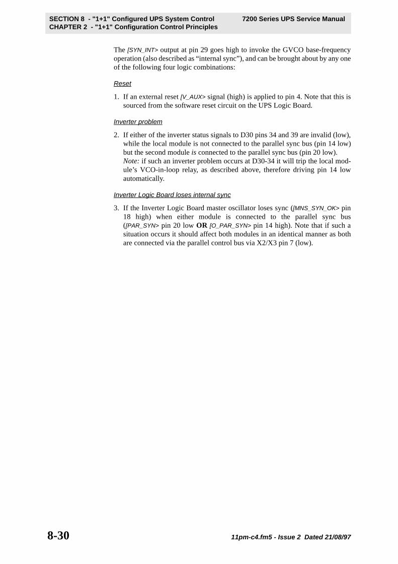
SECTION 8 - "1+1" Configured UPS System Control 7200 Series UPS Service ManualCHAPTER 2 - "1+1" Configuration Control Principles
The [SYN_INT> output at pin 29 goes high to invoke the GVCO base-frequencyoperation (also described as “internal sync”), and can be brought about by any oneof the following four logic combinations:
Reset
1. If an external reset [V_AUX> signal (high) is applied to pin 4. Note that this issourced from the software reset circuit on the UPS Logic Board.
Inverter problem
2. If either of the inverter status signals to D30 pins 34 and 39 are invalid (low),while the local module is not connected to the parallel sync bus (pin 14 low)but the second module is connected to the parallel sync bus (pin 20 low). Note: if such an inverter problem occurs at D30-34 it will trip the local mod-ule’s VCO-in-loop relay, as described above, therefore driving pin 14 lowautomatically.
Inverter Logic Board loses internal sync
3. If the Inverter Logic Board master oscillator loses sync ([MNS_SYN_OK> pin18 high) when either module is connected to the parallel sync bus([PAR_SYN> pin 20 low OR [O_PAR_SYN> pin 14 high). Note that if such asituation occurs it should affect both modules in an identical manner as bothare connected via the parallel control bus via X2/X3 pin 7 (low).
8-30 11pm-c4.fm5 - Issue 2 Dated 21/08/97
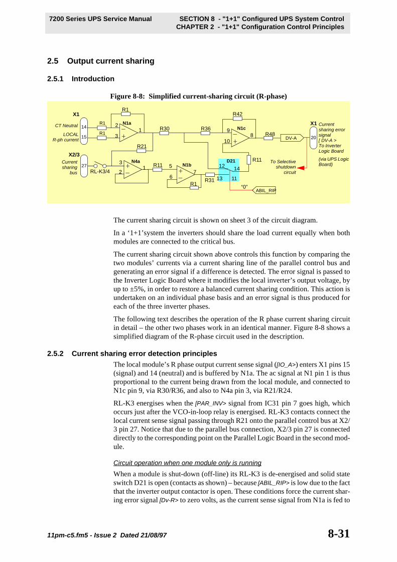
7200 Series UPS Service Manual SECTION 8 - "1+1" Configured UPS System ControlCHAPTER 2 - "1+1" Configuration Control Principles
Section 8:
2.5 Output current sharing
2.5.1 Introduction
Figure 8-8: Simplified current-sharing circuit (R-phase)
The current sharing circuit is shown on sheet 3 of the circuit diagram.
In a ‘1+1’system the inverters should share the load current equally when bothmodules are connected to the critical bus.
The current sharing circuit shown above controls this function by comparing thetwo modules’ currents via a current sharing line of the parallel control bus andgenerating an error signal if a difference is detected. The error signal is passed tothe Inverter Logic Board where it modifies the local inverter’s output voltage, byup to ±5%, in order to restore a balanced current sharing condition. This action isundertaken on an individual phase basis and an error signal is thus produced foreach of the three inverter phases.
The following text describes the operation of the R phase current sharing circuitin detail – the other two phases work in an identical manner. Figure 8-8 shows asimplified diagram of the R-phase circuit used in the description.
2.5.2 Current sharing error detection principles
The local module’s R phase output current sense signal ([IO_A>) enters X1 pins 15(signal) and 14 (neutral) and is buffered by N1a. The ac signal at N1 pin 1 is thusproportional to the current being drawn from the local module, and connected toN1c pin 9, via R30/R36, and also to N4a pin 3, via R21/R24.
RL-K3 energises when the [PAR_INV> signal from IC31 pin 7 goes high, whichoccurs just after the VCO-in-loop relay is energised. RL-K3 contacts connect thelocal current sense signal passing through R21 onto the parallel control bus at X2/3 pin 27. Notice that due to the parallel bus connection, X2/3 pin 27 is connecteddirectly to the corresponding point on the Parallel Logic Board in the second mod-ule.
Circuit operation when one module only is running
When a module is shut-down (off-line) its RL-K3 is de-energised and solid stateswitch D21 is open (contacts as shown) – because [ABIL_RIP> is low due to the factthat the inverter output contactor is open. These conditions force the current shar-ing error signal [Dv-R> to zero volts, as the current sense signal from N1a is fed to
N4a
12
3
RL-K3/4N1b
76
5
R1
R11
R31 13
12
11
14
N1a
12
3
R1
R1N1c
89
10
R42
R30R48
R36
R21
15
X1
LOCALR-ph current
27
X2/3
R114CT Neutral
D21 R11
20
X1 Current sharing error signal[ DV-A >To Inverter Logic Board
(via UPS Logic Board)
To Selectiveshutdown
circuit
“0”ABIL_RIP
Currentsharing
bus
DV-A
11pm-c5.fm5 - Issue 2 Dated 21/08/97 8-31

SECTION 8 - "1+1" Configured UPS System Control 7200 Series UPS Service ManualCHAPTER 2 - "1+1" Configuration Control Principles
N1c pins 9 and 10 in anti-phase and are self cancelling. Note: R10 and R11 are of equal value (3k9).
In a ‘redundant-module’ configured ‘1+1’ system it is permissible to operate onone module only (i.e. with the second module shut down). Under these conditionsD21’s contacts change over when the inverter output contactor is closed([ABIL_RIP> = 1) and the current sense signal at N1a pin 1 is now buffered by N4aand N1b and connected to N1c pin 10 via R31, D21 and R37.
However, R31 is of equal value to R30 (6K8), and once again the anti-phase sig-nals applied to IC1c pins 9 and 10 will be of equal magnitude and keep the errorsignal at 0V. Put simply, under these conditions the lone module attempts to cur-rent-share ‘with itself’ and is therefore never in error.
Note: In this scenario RL-K3 energises, and connects the current sense signal tothe current sharing bus line once the module is synchronised, but this has no affecton the current sharing circuit’s operation at this time as RL-K3 remains open inthe second (shut-down) module.
Current sharing operating under balanced conditions
When the second module is started, its current sense signal is applied to the cur-rent sharing parallel control bus X2/3 pin 27 (via its RL-K3).
Assuming that both modules are supplying exactly the same amount of load cur-rent, the current sense signal produced by N1a will be of the same amplitude andphase in both modules; therefore there will be no net current flow through R21 ineither module and thus no net voltage dropped across it.
Figure 8-9:
This is illustrated in Figure 8-9, where a current sense signal of 1Vac is assumedin both modules. Under these conditions the input signals to the error amplifier(N1c) are equal and produce zero [Dv-R> ‘error’ signals to the Inverter LogicBoard –these conditions are the same in both modules.
RL-K3
Module 1
N1a
1
R21
ErrorAmp
SenseAmp
X1
RL-K3
N1a
1
R21
27
Sense Amp
CN1
27
X2/X3
1Vac1Vac
Dv-R Dv-R
ErrorAmp
15
20
15
20
N1c8
9
10
N1c8
9
10Unbalanced current
Module 2
X2/X3
1Vac
8-32 11pm-c5.fm5 - Issue 2 Dated 21/08/97

7200 Series UPS Service Manual SECTION 8 - "1+1" Configured UPS System ControlCHAPTER 2 - "1+1" Configuration Control Principles
Current sharing operating under unbalanced conditions
Figure 8-10:
If the two modules supply different amounts of load current their current sensesignals at N1a will be different and there will be a net current flow along the cur-rent sharing parallel control bus, resulting in a voltage drop across R21 in eachmodule proportional to the degree of current imbalance.
This is depicted in Figure 8-10, which shows the situation where Module 1 is sup-plying more current than module 2.
In this case the current sharing control bus voltage (1.5Vac) is less than the cur-rent sense signal (2Vac) in module 1 but greater than the current sense signal(1Vac) in module 2. In Module 1 the voltage dropped across R1 produces a great-er voltage at N1c inverting input with respect to its non-inverting input and the[Dv-R> error signal (X1-20) will be a sinusoidal signal in anti-phase with the cur-rent sense signal.
In Module 2 however these conditions are reversed, with the greater voltage beingapplied to the non-inverting input of N1c, resulting in a [Dv-R> error signal whichis in-phase with the current sense signal.
The respective [Dv-R> error signals are applied to each module’s Inverter LogicBoard; and in this case the signal to Module 1 will cause a reduction of the outputvoltage and that to Module 2 will cause a corresponding increase – thus restoringa balanced load current condition.
Note: the above action is dynamic in operation and in practice the circuit effec-tively maintains a balanced state, with zero current flowing along the current shar-ing bus, at all times.
2.5.3 Current-sharing relay control (K3/K4)
Under normal circumstances, relays K3 and K4 are energised and de-energised atthe same time as the VCO-in-loop relays (K1/K2); in fact all four relay share acommon control signal – i.e. the [O_PAR_SYN> output from D30 pin 14 (see par-agraph 2.4.4.4 on page 8-28).
The only control difference between these two relay groups is that in the case ofthe current-sharing relays the [O_PAR_SYN> signal is gated with the TEST modelogic within D31 and the ultimate relay control signal ([PAR_INV>) is produced atD31 pin 7. [PAR_INV> is driven to a logic high to energise K3/K4 – this is invertedto a logic low at the relay driver D24 pin 13.
When the Parallel Logic Board is placed in its TEST mode (D31 in 43 taken low)the [PAR_INV> control signal at D31 pin 7 is forced to a permanent low logic stateto prevent the current sharing relays being energised. This is required in a redun-
RL-K3
Module 1
N1a
1
R21
ErrorAmp
SenseAmp
X1
RL-K3
N1a
1
R21
27
Sense Amp
CN1
27
X2/X3
1Vac2Vac
1.5VacDv-R Dv-R
ErrorAmp
15
20
15
20
N1c8
9
10
N1c8
9
10Unbalanced current
Module 2
X2/X3
11pm-c5.fm5 - Issue 2 Dated 21/08/97 8-33

SECTION 8 - "1+1" Configured UPS System Control 7200 Series UPS Service ManualCHAPTER 2 - "1+1" Configuration Control Principles
dant module system to allow an off-line module to be tested without affecting thecurrent-sharing function of the second (on-line) module.
2.5.4 Selective shutdown
The Selective Shutdown circuit, which is shown on sheet 3 of the circuit dia-grams, monitors the current-sharing circuit output signals together with outputphase voltage sense signals and detects three types of current-related fault condi-tions:
1. It detects when the current sharing is in error and calling for the local moduleto provide an excessive amount of current in comparison to the other module.
2. It detects an excess ‘reverse power’ condition whereby a fault in the localmodule is causing it to draw current into its output terminals from the othermodule.
3. It detects an excess ‘forward power’ condition whereby a fault in the localmodule is causing it to feed current into the output terminals of the othermodule.
Considering the R phase circuit: the current error signal produced at N1c pin 8([Dv-A>), described on the previous pages, is fed to N1d pin 13 via R48 where itis summed with a sense signal proportional to the module’s output R-phase volt-age ([VO_A>). The ‘VA-proportional’ output from N1d pin 14 is connected to athree-phase full-wave rectifier, along with the corresponding S and T phase sig-nals (V1-V6), which then produces a single VA-related signal across R61 whichis proportional to the module’s three phase output.
Under balanced conditions the current error signal [Dv-A> is negligible; and theoutput from N1 pin 14 is directly proportional to the voltage sense signal. Undersuch circumstances the bridge rectifier produces approximately 4.1V at N5 pin 1.
2.5.4.1 Current-sharing error
If the current sharing function fails to operate correctly and calls for this moduleto produce an excessive amount of current in comparison to the second module,the [DV-R> [DV-S> [DV-T> signal(s) add to the voltage-related signals and result inan increased output from IC5a pin 1.
This is monitored by N5d whose output goes high if N5a pin 1 rises above 5.0V(equivalent to 30% of nominal current sharing imbalance) – i.e. if the module isbeing asked to produce 30% of nominal load capacity more than the second mod-ule. The resulting logic high [IN_SEL> signal flags D31 pin 4 which turns off theinverter and trips the output contactor (see paragraph 2.3.1.1 on page 8-13).
Calibration
N5d’s switching threshold is determined by a reference voltage generator (N11)whose output voltage is calibrated by R19. This resistor should be adjusted ac-cording to the module’s working voltage to obtain the following dc voltage at thetop of R68 (junction with R72):
380V = 5.0 Vdc400V = 5.26 Vdc415V = 5.46 Vdc
8-34 11pm-c5.fm5 - Issue 2 Dated 21/08/97

7200 Series UPS Service Manual SECTION 8 - "1+1" Configured UPS System ControlCHAPTER 2 - "1+1" Configuration Control Principles
2.5.4.2 Reverse Power detector
If the local module’s output voltage suddenly decreases due to an internal faultcondition it will begin to take reverse current from the second module. Underthese circumstances the current sense signals will be out of phase with, and there-fore subtract from, the voltage sense signals. The VA signal at N5a pin 1 willtherefore reduce and ultimately fall below the operating threshold of N5c, whoseoutput will in turn go high and invoke the [IN_SEL> shutdown signal with the sameresults as the current error situation described above.
Due to the current imbalance, the current-sharing circuit in the second modulewill call for it to reduce its output voltage, and the falling voltage sense signalswill cancel out the increasing forward current signals. Thus the [IN_SEL> signal isnot triggered in the second module and the healthy module will not be tripped off-line in a ‘redundant module’ system. However, in a ‘non-redundant’ system thesecond module will trip of line automatically along with the faulty local module.
Calibration
This function shares the same calibration features as the current-sharing error cir-cuit described previously.
2.5.4.3 Forward Power detector
If the local module’s output voltage suddenly increases due to an internal faultcondition it will attempt to supply all the load current and also feed a reverse cur-rent into the second module. Under these circumstances, in the local module, thesummation of the VA signals at N5 pin 1 triggers the upper level detector N5d andthe [IN_SEL> signal is activated in the same manner as described for a ‘current-sharing’ fault.
Due to the current imbalance, the current sharing circuit in the second module willcall for it to increase its output voltage and the rising voltage sense signals willcancel out the decreasing reverse current signals. Thus the [IN_SEL> signal is nottriggered in the second module and the healthy module is not tripped off-line in a‘redundant module’ system.
In a non-redundant system the second module will trip of line automatically alongwith the faulty local module. However, in a ‘non-redundant’ system the secondmodule will trip of line automatically along with the faulty local module.
2.5.5 On-line module counter
This circuit, shown on sheet 2 of the circuit diagrams, detects the number of on-line modules and is used in a ‘redundant system’ to inhibit the selective shutdowncircuit within D31 when only one module is on-line – i.e. if only one module isrunning, and by definition providing all the load current, there is no valid reasonto allow its current sharing circuit to produce a selective shutdown and trip themodule off-line (see paragraph 2.3.1.1 on page 8-13).
When a module is brought on-line, the signal used to energise the VCO-in-looprelays (K1/K2) is also fed to the module counter circuit as [PAR_INV>. This signalgoes high when the module is on-line, whereupon it turns on V43 and V42 whichprovides a current source whatever resistance value is selected by jumpers X5. Ina standard configuration X5 jumpers 1/2/3 are made. This in turn causes a voltagerise to the non-inverting input of comparator N9b (pin 5) via R130.
<O_N_INV> is connected to the parallel control bus via X2/3 pin 24, thereforewhen both modules are on-line the current passing through the selected resistancedoubles, with a corresponding increase to the voltage offered to the comparator.
11pm-c5.fm5 - Issue 2 Dated 21/08/97 8-35

SECTION 8 - "1+1" Configured UPS System Control 7200 Series UPS Service ManualCHAPTER 2 - "1+1" Configuration Control Principles
The comparator’s operating threshold is determined by the resistance selected byX4. In a standard 1+1 configuration X4 jumper 1 only is fitted, which sets the cir-cuit operation such that [C_N_INV> switches high only when both modules are online, and is low at all other times.
Note: the reason for the additional jumper positions on X4 and X5 is to allow thisboard to be used in a multi-module system, where up to six modules can co con-nected in a parallel-operating configuration. Where such a system is used, X4 andX5 permit the minimum number of on-line modules necessary to retain system in-tegrity to be programmed.
2.6 Parallel rectifier operation
2.6.1 Rectifier current-sharing control
If a single stand-by battery bank is used by both modules the installation is de-scribed as having a ‘common battery’, and in this situation steps are taken toensure that both modules contribute an equal amount of battery charge current.
A current sharing circuit, similar to that used to control the output current sharing,is employed to ensure that both modules’ rectifiers take an equal amount of inputcurrent. Consequently, if the modules’ input currents are equal and their outputcurrents are equal this implies that they are properly sharing the battery chargecurrent.
The local module’s input current sense signal ([I_RECT_T>) enters X1 pin 24 andis buffered by N6a. The signal at N6a pin 1, is then connected to N6b pin 6 andalso to N6c pin 10 via R66.
If the local module is the only module on-line, as part of a redundant module sys-tem, the inputs to N6b pins 5 and 6 will cancel each other as they are both obtainedfrom the same source – e.g. pin 6 monitors the current sense signal from N6 pin1 and pin 5 monitors the same signal via a second buffer (N6c). Under such cir-cumstances the output from N6b pin 7 is zero, which then produces a zero errorsignal output ([DB>) at X1 pin 25. X1 pin 25 is connected to the voltage regulationcontrol circuit on the Rectifier Logic Board, via a through connection on the UPSLogic Board, and trims the rectifier voltage as necessary to adjust its input cur-rent.
Rectifier current sharing is enabled by energising relay K5. This removes theground inhibit from N6d non-inverting input and also connects the local currentsense signal (<IM_R>) passing through R66 to the current sharing bus connectedto X2/3 pin 26.
When the second module is started, its input current sense signal is applied to theparallel control bus X2/3 pin 26 in the same manner as described for the localmodule. Assuming that both modules are drawing exactly the same amount ofinput current, there will be no net current flow through R55 in either module, re-sulting in zero output from IC8b pin 7.
If the modules draw different amounts of input current their current sense signalsdiffer and there will be a net current flow along the parallel control bus resultingin a volts drop across R66 proportional to the current imbalance in each module.
This will be detected by N6c, whose output will increase [DB> in the moduledrawing less current and decrease [DB> in the other. This processes is continuousand results in close input current sharing between the two modules at all timesunder normal conditions.
8-36 11pm-c5.fm5 - Issue 2 Dated 21/08/97

7200 Series UPS Service Manual SECTION 8 - "1+1" Configured UPS System ControlCHAPTER 2 - "1+1" Configuration Control Principles
Relay K5 control
As mentioned above, relay K5 must be energised in order to activate the rectifiercurrent sharing function; this is achieved by the [O_PAR_REC> output from D30pin 17 going high. D30 pin 17 is itself controlled by the [PAR_REC> input to D30pin 32 which is derived from the UPS Logic Board micro controller system andgoes high to select parallel rectifier operation – i.e. when the UPS Logic Board isprogrammed to invoke rectifier current sharing (common battery) it sends a logichigh [PAR_REC> signal to D30 pin 32 whose [O_PAR_REC> output then switcheshigh to energise relay K5. This can be overridden by jumper X6-2 which, whenmade, clamps [O_PAR_REC> to a logic low. X6-2 is used to select ‘parallel’ or‘non-parallel’ rectifier operation (open for non-parallel operation) and also affectsthe boost charge and battery test functions as described below.
2.6.2 Boost charge control
In a common battery system it is not permissible to have one module operating inthe boost charge mode while the other is in float charge, otherwise they will beunable to share the battery charge current.
‘Boost’ charge is requested by the UPS Logic Board’s micro controller systemwhich applies a logic high [O_BST_BAT> input to X1 pin 47. This is connected tothe parallel control bus via X2/3 pin 8 ([B_BST_BAT>), and also to D30 pin 24([BST_BAT>). Sending the signal through the parallel control bus thus drives the[BST_BAT> signal high in both modules if either module requests boost charge.
When [BST_BAT> goes high it drives D30 pin 16 high, which is then connectedback to the UPS Logic Board via X1 pin 35 ([I_BST_BAT>) to inform the UPSLogic Board that the request has been acknowledged. The UPS Logic Board willthen initiate the boost charge mode via appropriate signalling to the RectifierLogic Board. Therefore, in a parallel rectifier configured system both rectifiersare triggered into the boost mode.
If parallel rectifier operation is not required then jumper X6-2, when fitted, willoverride the boost charge request logic within D30 and clamp the output on D30pin 16 at logic low. In this situation the signal passed along the parallel controlbus will have no effect in either module and the boost mode will be independentlycontrolled for each rectifier.
2.6.3 Battery test control
In a common battery system it is not permissible to have one module operating inthe battery mode without the other, otherwise they will be unable to share the bat-tery charge current. A control mechanism similar to the boost charge circuit de-scribed immediately above is therefore used to prevent this from happening.
‘Battery Test’ is requested by the UPS Logic Board’s micro controller systemwhich applies a logic high [O_TST_BAT> input to X1 pin 46. This is connected tothe parallel control bus via X2/3 pin 13 ([B_TST_BAT>), and also to D30 pin 21([TST_BAT>). Sending the signal through the parallel control bus thus drives the[TST_BAT> signal high in both modules if either module requests a Battery Test.
When [TST_BAT> goes high it drives D30 pin 19 high, which is then connectedback to the UPS Logic Board via X1 pin 36 ([I_TST_BAT>) to inform the UPSLogic Board that the request has been acknowledged. The UPS Logic Board willthen initiate the Battery Test via appropriate signalling to the Rectifier LogicBoard. Therefore, in a parallel rectifier configured system both rectifiers are trig-gered into the Test mode.
11pm-c5.fm5 - Issue 2 Dated 21/08/97 8-37

SECTION 8 - "1+1" Configured UPS System Control 7200 Series UPS Service ManualCHAPTER 2 - "1+1" Configuration Control Principles
If parallel rectifier operation is not required then jumper X6-2, when fitted, willoverride the Battery Test request logic within D30 and clamp the output on D30pin 19 at logic low. In this situation the signal passed along the parallel controlbus will have no effect in either module and the Battery Test mode will be inde-pendently controlled for each rectifier.
2.7 Other Features and functions
2.7.1 Ribbon cable connection monitor
As mentioned on page 8-13, the Parallel Logic Board senses the parallel controlbus integrity by monitoring the continuity of the two ribbon cables fitted X2 andX3, which are cross connected between the two modules. The modules’ paralleloperation can be maintained if one of these cables becomes disconnected (inwhich event Led H2 illuminates), but if both cables become disconnected then theParallel Logic Board demands that the module inverters are shut-down and theload transferred to bypass.
Monitoring the cables’ continuity is made possible due to the way that the cablesare cross-connected between the two modules; the error detection signals are an-notated [A_CON> and [B_CON> (see page 4 of the circuit diagrams). For example,the [A_CON> signal at X2 pin 1 is held at 0V due to the fact that pin 1 of X3 in thesecond module is grounded – the same principle applies to the [B_CON> signal atX3 pin 2. Thus, the Parallel Logic Board can detect if a ribbon cable is discon-nected at either end.
8-38 11pm-c5.fm5 - Issue 2 Dated 21/08/97

7200 Series UPS Service Manual SECTION 8 - "1+1" Configured UPS System ControlCHAPTER 2 - Parallel Logic Board
Section 8:
2.8 Parallel Logic Board circuit operation during start-up
When the UPS system is started, there are distinct phases that the module goesthrough before the load is connected to the inverter(s). These can broadly be de-scribed as:
• Initialisation/reset
• Run-up & inverter synchronisation
• Connecting to the parallel control bus
• Load transfer procedure (depending on system redundancy)
These phases are described in detail below and aims to give a full understandingof the system start-up process to facilitate system troubleshooting.
2.8.1 Initialisation/reset
When a module is first started, its UPS Logic Board micro-system goes througha power-up reset and initialisation routine which applies a 1-second logic highpulse to X1-42 ([V_AUX>). The effects of this are:
1. D31-5 goes high to reset the ‘selective shutdown’ circuit latch (D31-37 setlow and led H1 = off) (See paragraph 2.3.1.1)
2. D30-4 goes high which:
a) drives D30-29 ([SYN_INT>) high which forces the GVCO to its ‘internalsync’ mode – (See paragraph 2.4.4.5).
b) drives D30-38 & D30-14 low to reset the VCO-in-loop control logic andensure the VCO-in-loop relays (K1/K2) are de-energised ([O_PAR_SYN> =low) – (See paragraph 2.4.4.4).
3. D30-14 ([O_PAR_SYN>) going low is connected to D31-24 where it drivesD31-21 ([RIP>) high which is inverted to a logic low [PAR_INV> at D28-4which then:
a) de-energises the current-sharing relays (K3/K4).
b) informs the ‘available modules counter’ circuit that the module is off-line.
c) places a logic low input to D31-7 which enables the ‘load-on-bypass’request from D31-18 (low) and disables the ‘load-on-inverter’ requestfrom D31-12 (high) (See paragraph 2.3.2).
d) feeds a logic low input to D30-26 which enables the [INV_OK> signalapplied to D31-39 within D31.
2.8.2 Inverter run-up and synchronisation
1. Provided the UPS power switches and parallel bus cables are positioned cor-rectly, at the culmination of the reset action D31-19 ([OFF_INV>) should golow, requesting the inverter to run (See paragraph 2.3.1)
2. If other parameter on the UPS Logic Board are satisfactory, the invertershould now start and its voltage should begin to rise to nominal value; duringwhich time the following events occur:
a) [O_MNS_SYN> to D30 pins 8 and 18 go low when the Inverter LogicBoard’s master oscillator gains internal sync. The input to pin 8 is associ-
11pm-c6.fm5 - Issue 2 Dated 21/08/97 8-39

SECTION 8 - "1+1" Configured UPS System Control 7200 Series UPS Service ManualCHAPTER 2 - Parallel Logic Board
ated with the bypass frequency validation circuit (See paragraph 2.4.4.1)and the input to pin 18 with the GVCO ‘internal sync’ logic – although[SYN_INT> is still high, requesting “internal sync” at this time due to thestill logic low [INV_OK> input to D30 pin 34 (See paragraph 2.4.4.5).
b) The [BLK_INV> input to D30 pin 34 is high, indicating that there is no faultdetected on the Inverter Logic Board – once again this has no effect onD31 internal operation due to the logic low [INV_OK> input to D30 pin 34.
2.8.3 Connecting to the parallel control bus
When the inverter output voltage rises to its nominal value the [INV_OK> input toD30 pin 39 will go high, and initiate the following sequence of events:
1. The [SYN_INT> output from D30-29 will go low to enable the GVCO’s ‘angleregulator’ circuit, allowing the GVCO to synchronise to the selected[FRQ_REF> signal (See paragraph 2.4.4.5).
2. Provided the synchronisation functions are satisfied, the VCO-in-loop relays(K1/K2) will be energised by D30-14 ([O_PAR_SYN>) going high. The syn-chronisation functions vary according to whether the module is the “first” or“second” module to be started and is described in details in paragraph 2.4.4.4.If K1/K2 fail to energise at this stage it is recommended that you read andthoroughly understand paragraph 2.4.4.4 before going further.
3. D30-14 ([O_PAR_SYN>) going high is connected to D31-24 where it drivesD31-21 ([RIP>) low which is inverted to a logic high [PAR_INV> at D28-4which then:
a) energises the current-sharing relays (K3/K4).
b) feeds a logic high input to D30-26 which disables the effects of the[INV_OK> input to D31-39 within D31.
c) informs the ‘available modules counter’ circuit that the module is con-nected to the parallel control bus and available for use.
d) places a logic high [PAR_INV> input to D31-7 which disables the ‘load-on-bypass’ request from D31-18 (now switches high) and enables the ‘load-on-inverter’ request from D31-12 (although D31-12 is not driven low dueto this signal at this point – see below).
2.8.4 Load transfer to inverter
The point at which the load is transferred to the inverter depends on whether theParallel Logic Board is configured for a ‘redundant’ or ‘non-redundant’ systemoperation – i.e. jumper X6-3 closed = ‘redundant’ configuration and X6-1 closed= ‘non-redundant’.
The difference between these configuration is that in a ‘redundant’ system theload can be allowed to transfer to inverter when only one module is running, butin a ‘non-redundant’ system both modules have to be running before the load isallowed to transfer. The effects of the configuration on the transfer circuit opera-tion are described below.
‘Redundant’ system transfer operation
1. In a ‘redundant module’ configuration the ‘available module counter’ circuitis configured such that its [C_N_INV> output switches high when only onemodule is connected to the parallel control bus. Thus, in such a system this
8-40 11pm-c6.fm5 - Issue 2 Dated 21/08/97

7200 Series UPS Service Manual SECTION 8 - "1+1" Configured UPS System ControlCHAPTER 2 - Parallel Logic Board
occurs at this point in the start-up sequence.
2. The effects of the logic high [C_N_INV> input to D31-27, coupled with thelogic high [PAR_INV> input to D31-7 now make D31-12 ([C_L_INV>) switchlow, sending a ‘load-on-inverter’ request to the UPS Logic Board.
3. If the UPS Logic Board conditions are normal it should now send a ‘transferto inverter’ command to the Static Switch Driver Board which will closed theinverter output contactor and turn off the static bypass SCRs.
‘Non-redundant’ system transfer operation
4. In a ‘non-redundant’ system two sets of signals, each of which detects theavailability of both modules on the parallel control bus, are required by thetransfer control logic before the load is allowed to transfer to the inverter.
a) In a ‘non-redundant module’ configuration the ‘available module counter’circuit is configured such that its [C_N_INV> output switches high onlywhen both modules are connected to the parallel control bus
b) The logic high [PAR_INV> input to D31-7 is inverted to a logic low[O_INV_IND> at D31-8. This is inverted to a high at D24-17 from where itis connected to the parallel control bus via X2/X3 pin 12. Due to the paral-lel control bus, the [INV_IND> input to D31-29 is thus logic low only ifboth modules are available (i.e. if [O_INV_IND> is low in both modules).
5. The effects of the logic high [C_N_INV> input to D31-27, coupled with thelogic high [PAR_INV> input to D31-7 and low [INV_IND> input to D31-29, nowmake D31-12 ([C_L_INV>) switch low, sending a ‘load-on-inverter’ request tothe UPS Logic Board.
6. If the UPS Logic Board conditions are normal it should now send a ‘transferto inverter’ command to the Static Switch Driver Board which will closed theinverter output contactor and turn off the static bypass SCRs.
Applicable to both system configurations
7. Once the load has transferred to the inverter two key signals are sent backfrom the UPS Logic Board to the Parallel Logic Board:
a) First, a lockout signal slaved to the inverter output contactor auxiliary con-tacts applies a logic high [N_AUX_CONT> input to D31-34 which preventsthe ‘load on bypass’ request from being generated at D31-18 while thecontactor is closed.
b) Second, a logic high ‘inverter on load’ status signal ([INV_L>) is fed backto X1-52 which is connected to:– D31-31 (low) to enable the ‘selective shutdown’ circuit within D31.– D31-25 (high) to provide a second lockout to the ‘load on bypass’request circuit within D31 in the same manner as [N_AUX_CONT>
described above.– via a debounce circuit, [INV_L> produces a logic high [ABIL_RIP> signalwhich energises the current-sharing circuit solid-state switches to activatethe current-sharing facility (See paragraph 2.5.2).
8. The UPS Module is now running and on-line, and its synchronisation andload-sharing signals are connected to the second module via the parallel con-trol bus.
11pm-c6.fm5 - Issue 2 Dated 21/08/97 8-41

SECTION 8 - "1+1" Configured UPS System Control 7200 Series UPS Service ManualCHAPTER 2 - Parallel Logic Board
2.8.5 Load retransfer back to bypass
Under normal circumstances the load should remain on inverter at all times, andtransfer back to the bypass supply only if inverter is no longer available. There areseveral mechanisms which can initiate a ‘transfer to bypass’ request, as outlinedbelow.
Loss of one module in a ‘non-redundant’ system
This condition will be detected by the ‘available module counter’ circuit([C_N_INV> = low) – and once the faulty module has tripped off-line, also by theparallel bus line X2/X3-12 which will produce a low [INV_IND> to D31-29.
Either of these signals will send D31-12 high, removing the ‘load on inverter’ re-quest to the UPS Logic Board which will respond by providing a logic low[INV_L> signal to D31-25 which drives D31-18 low to produce a ‘load on bypass’request.
Note: Once the inverter output contactor opens the ‘load on bypass’ request is sus-tained by the inverter output contactor auxiliary contacts which now hold D31-34high.
Inverter Block [BLK_INV>
If the [BLK_INV> input to D30-34 is driven low by the UPS Logic Board, eitherdue to an inverter fault or selected shutdown etc, it drives D30-14 ([O_PAR_SYN>)low which then drives D31-21 ([RIP>) high and releases K1/K2 (and by associa-tion also K3/K4) to trip the module off the parallel control bus.
This also provides a low [PAR_INV> input to D31-7 which disables the ‘load oninverter’ request. The effects of this are as described above.
Note: if any of the signals which affect the [O_PAR_SYN> output from D30-12switch to a fault level it has the same effects as the [BLK_INV> signal going low, asdescribed,
2.9 Test mode of operation:
A test facility is built into the Parallel Logic Board control system which allowsthe module to be fully run up without its output being connected to the system –i.e. in a ‘redundant module’ system this facilitates the full testing of one modulewhilst the other remains on-line to provide the load supply.
The test mode is activated by fitting jumper X6-1, which pulls D31-43 down to0v (logic low) with the following affects:
1. It interlocks with the [SW_OUT> input to D31-14 such that the [OFF_INV> out-put at D31-19 is allowed to turn the inverter on (low) only if the module’soutput switch is open.
2. It forces D31-21 ([RIP>) high which ensures that relays K1/K2 (and by asso-ciation K3/K4) remain open. This prevents placing a faulty module onto theparallel control bus synchronisation and current-sharing lines.
3. If forces D31-12 ([C_L_INV>) low to provide the UPS Logic Board with acontinuous ‘load on inverter’ request. This overrides all other inputs to D31normally required to generate such a request.
4. It disables the selective shutdown logic within D31.
8-42 11pm-c6.fm5 - Issue 2 Dated 21/08/97