Embed Size (px)
DESCRIPTION
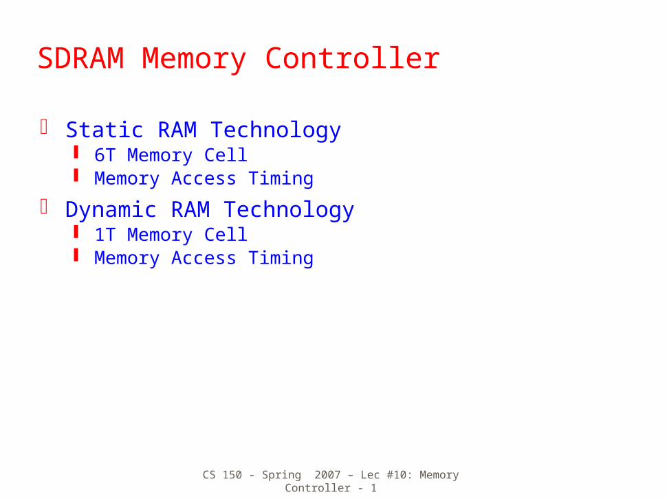
SDRAM Memory Controller. Static RAM Technology 6T Memory Cell Memory Access Timing Dynamic RAM Technology 1T Memory Cell Memory Access Timing. +. +. In X 0 1. OE_L 1 0 0. Out Z 0 1. IN. OUT. IN. OUT. OE_L. OE_L. OUT. OUT. OE_L. OE_L. IN. IN. 0. 0. Tri-State Gates. - PowerPoint PPT Presentation
Citation preview
CS 150 - Spring 2007 – Lec #10: Memory Controller - 1
SDRAM Memory Controller
Static RAM Technology 6T Memory Cell Memory Access Timing
Dynamic RAM Technology 1T Memory Cell Memory Access Timing
CS 150 - Spring 2007 – Lec #10: Memory Controller - 2
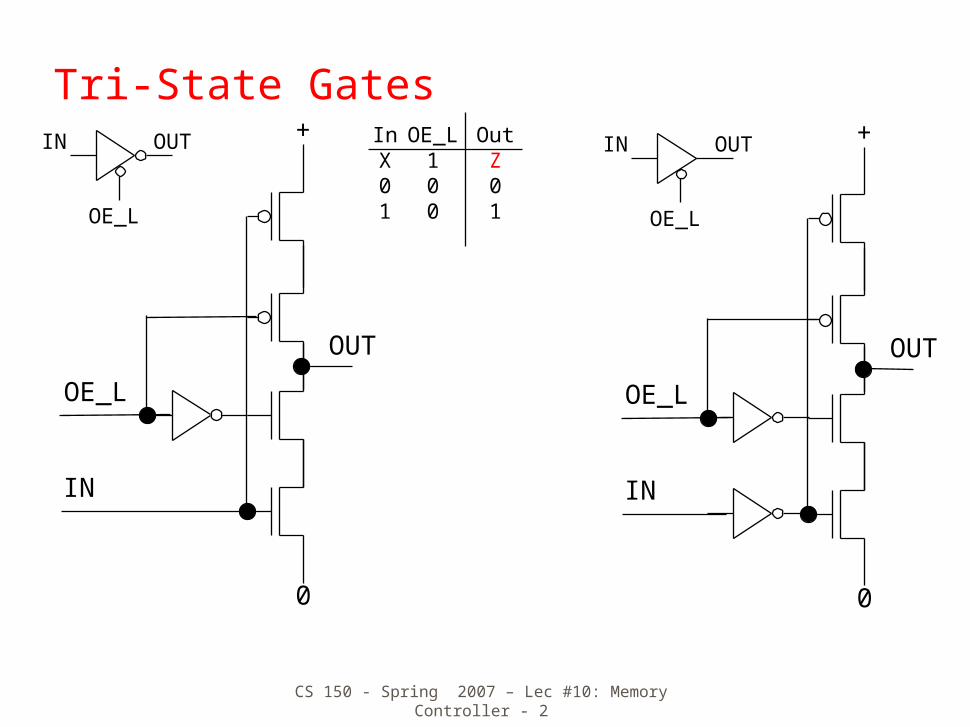
Tri-State Gates
OE_L
IN
OUT
+
0
IN OUT
OE_L
OUTIN
OE_L
OE_L
IN
OUT
+
0
InX01
OE_L100
OutZ01
CS 150 - Spring 2007 – Lec #10: Memory Controller - 3
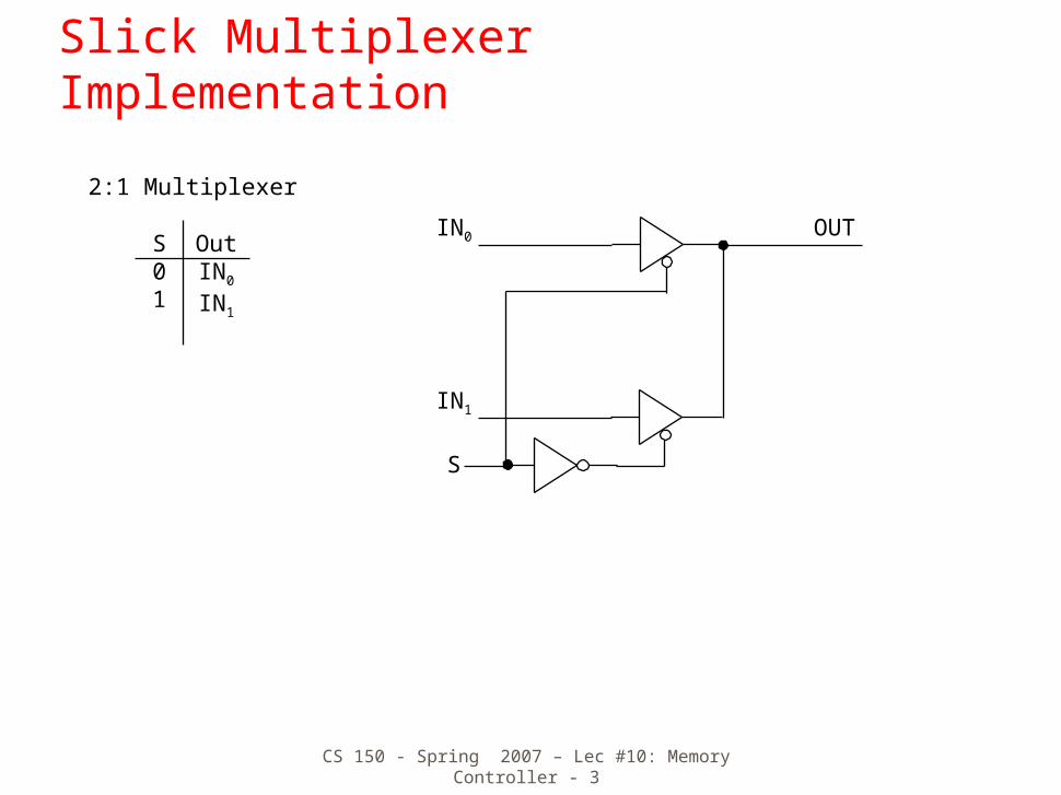
Slick Multiplexer Implementation
OUTIN0
IN1
S
2:1 Multiplexer
S01
OutIN0
IN1

CS 150 - Spring 2007 – Lec #10: Memory Controller - 4
Basic Memory Subsystem Block Diagram
AddressDecoder
Word Line
n AddressBits
2n wordlines
m Bit Lines
Memorycell
what happensif n and/or m isvery large?
CS 150 - Spring 2007 – Lec #10: Memory Controller - 5
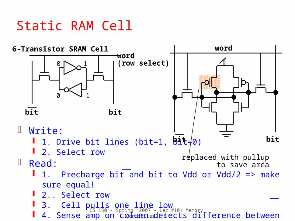
Static RAM Cell
Write: 1. Drive bit lines (bit=1, bit=0) 2. Select row
Read: 1. Precharge bit and bit to Vdd or Vdd/2 => make sure
equal! 2.. Select row 3. Cell pulls one line low 4. Sense amp on column detects difference between bit
and bit
6-Transistor SRAM Cell
bit bit
word(row select)
bit bit
word
replaced with pullupto save area
10
0 1
CS 150 - Spring 2007 – Lec #10: Memory Controller - 6
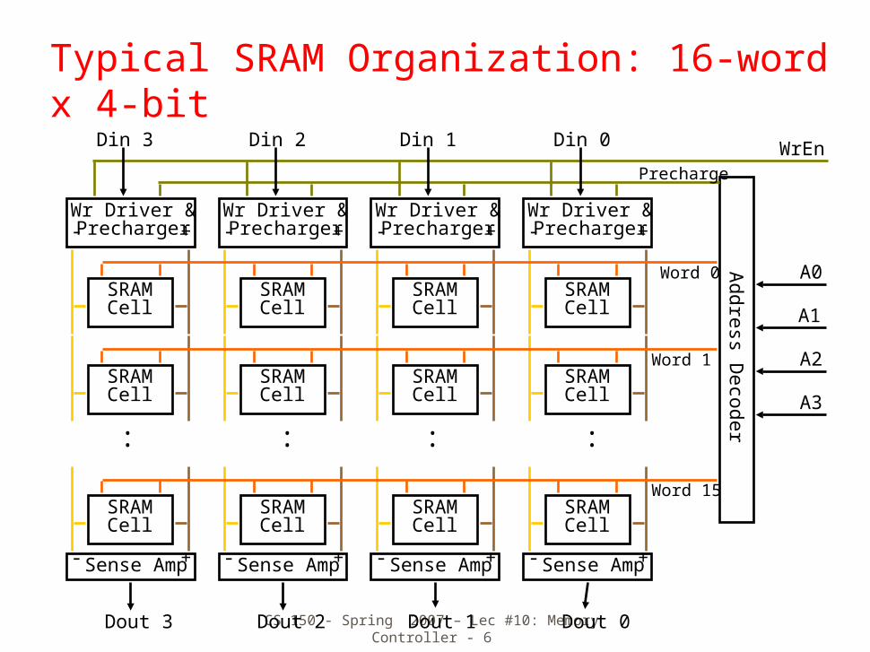
Typical SRAM Organization: 16-word x 4-bit
SRAMCell
SRAMCell
SRAMCell
SRAMCell
SRAMCell
SRAMCell
SRAMCell
SRAMCell
SRAMCell
SRAMCell
SRAMCell
SRAMCell
- +Sense Amp - +Sense Amp - +Sense Amp - +Sense Amp
: : : :
Word 0
Word 1
Word 15
Dout 0Dout 1Dout 2Dout 3
- +Wr Driver &Precharger - +
Wr Driver &Precharger - +
Wr Driver &Precharger - +
Wr Driver &Precharger
Addre
ss Deco
der
WrEnPrecharge
Din 0Din 1Din 2Din 3
A0
A1
A2
A3
CS 150 - Spring 2007 – Lec #10: Memory Controller - 7
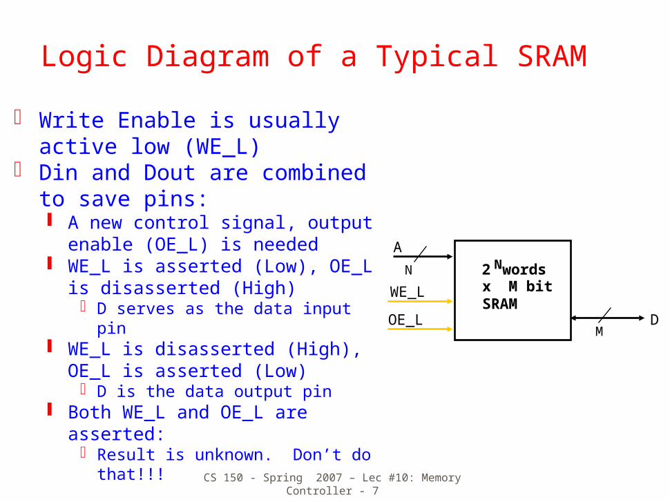
Write Enable is usually active low (WE_L)
Din and Dout are combined to save pins: A new control signal, output
enable (OE_L) is needed WE_L is asserted (Low), OE_L is
disasserted (High) D serves as the data input pin
WE_L is disasserted (High), OE_L is asserted (Low)
D is the data output pin Both WE_L and OE_L are
asserted: Result is unknown. Don’t do
that!!!
A
DOE_L
2Nwordsx M bitSRAM
N
M
WE_L
Logic Diagram of a Typical SRAM
CS 150 - Spring 2007 – Lec #10: Memory Controller - 8
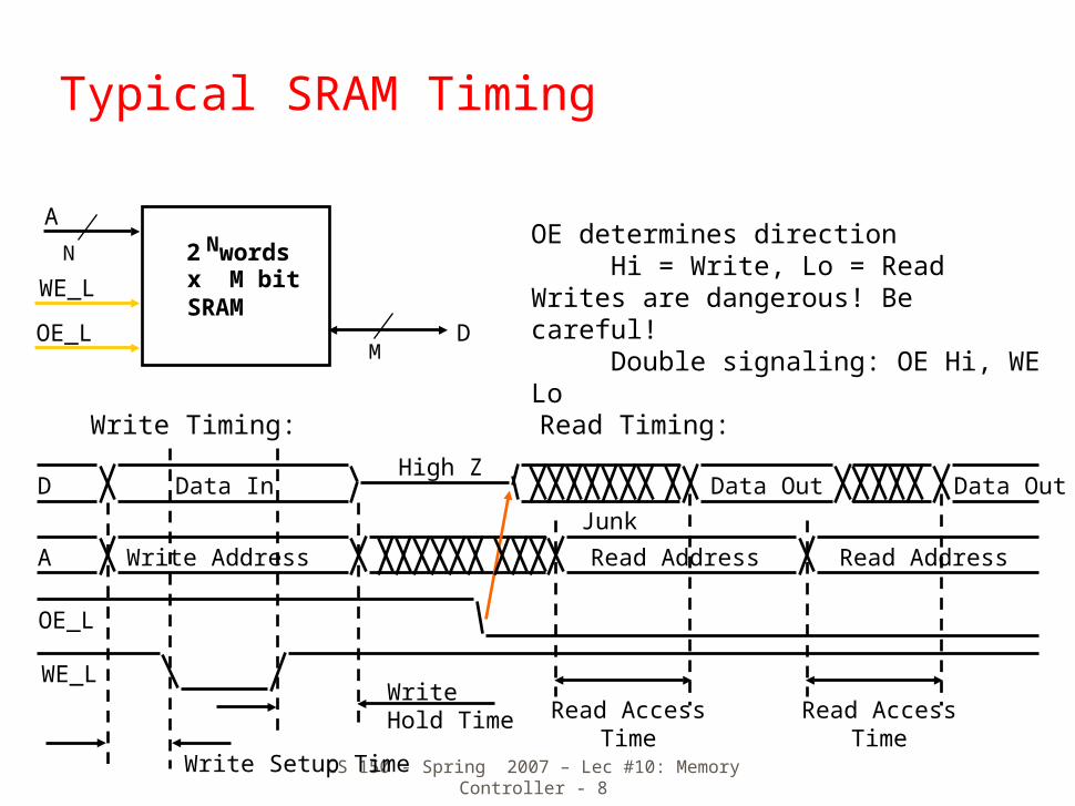
Typical SRAM Timing
Write Timing:
D
Read Timing:
WE_L
A
WriteHold Time
Write Setup Time
A
DOE_L
2Nwordsx M bitSRAM
N
M
WE_L
Data In
Write Address
OE_L
High Z
Read Address
Junk
Read AccessTime
Data Out
Read AccessTime
Data Out
Read Address
OE determines direction Hi = Write, Lo = ReadWrites are dangerous! Be careful! Double signaling: OE Hi, WE Lo
CS 150 - Spring 2007 – Lec #10: Memory Controller - 9
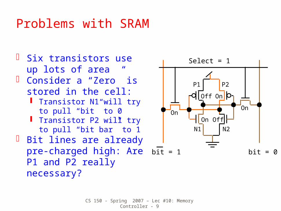
Problems with SRAM
Six transistors use up lots of area
Consider a “Zero” is stored in the cell: Transistor N1 will try to pull
“bit” to 0 Transistor P2 will try to pull
“bit bar” to 1 Bit lines are already pre-
charged high: Are P1 and P2 really necessary?
bit = 1 bit = 0
Select = 1
On Off
Off On
N1 N2
P1 P2
OnOn
CS 150 - Spring 2007 – Lec #10: Memory Controller - 10
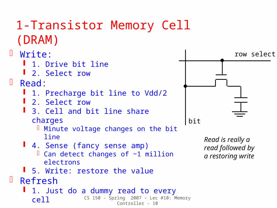
1-Transistor Memory Cell (DRAM)
Write: 1. Drive bit line 2. Select row
Read: 1. Precharge bit line to Vdd/2 2. Select row 3. Cell and bit line share charges
Minute voltage changes on the bit line 4. Sense (fancy sense amp)
Can detect changes of ~1 million electrons
5. Write: restore the value Refresh
1. Just do a dummy read to every cell
row select
bit
Read is really aread followed bya restoring write
CS 150 - Spring 2007 – Lec #10: Memory Controller - 11
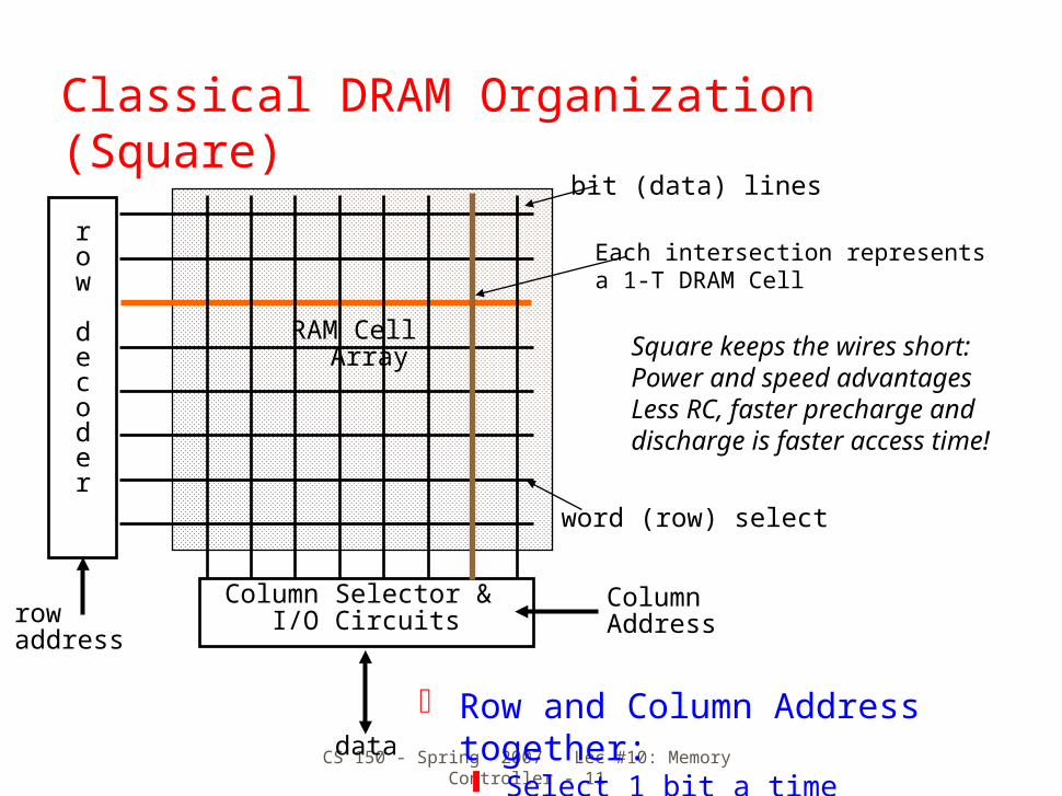
Classical DRAM Organization (Square)
row
decoder
rowaddress
Column Selector & I/O Circuits
ColumnAddress
data
RAM Cell Array
word (row) select
bit (data) lines
Row and Column Address together: Select 1 bit a time
Each intersection representsa 1-T DRAM Cell
Square keeps the wires short:Power and speed advantagesLess RC, faster precharge anddischarge is faster access time!
CS 150 - Spring 2007 – Lec #10: Memory Controller - 12
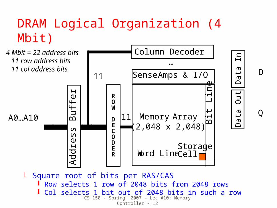
DRAM Logical Organization (4 Mbit)
Square root of bits per RAS/CAS Row selects 1 row of 2048 bits from 2048 rows Col selects 1 bit out of 2048 bits in such a row
Column Decoder
Sense Amps & I/O
Memory Array(2,048 x 2,048)
A0…A10
…
11 D
Q
Word LineStorage Cell
ROW
DECODER
11
4 Mbit = 22 address bits 11 row address bits 11 col address bits
Ad
dre
ss B
uff
er
Bit
Lin
e
Data
In
Data
Ou
t
CS 150 - Spring 2007 – Lec #10: Memory Controller - 13
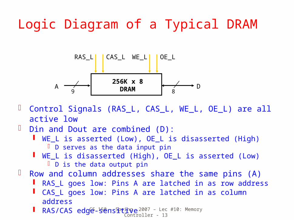
A D
OE_L
256K x 8DRAM9 8
WE_L
Control Signals (RAS_L, CAS_L, WE_L, OE_L) are all active low Din and Dout are combined (D):
WE_L is asserted (Low), OE_L is disasserted (High) D serves as the data input pin
WE_L is disasserted (High), OE_L is asserted (Low) D is the data output pin
Row and column addresses share the same pins (A) RAS_L goes low: Pins A are latched in as row address CAS_L goes low: Pins A are latched in as column address RAS/CAS edge-sensitive
CAS_LRAS_L
Logic Diagram of a Typical DRAM
CS 150 - Spring 2007 – Lec #10: Memory Controller - 14
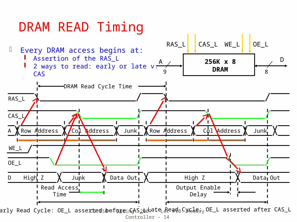
A D
OE_L
256K x 8DRAM9 8
WE_LCAS_LRAS_L
OE_L
A Row Address
WE_L
Junk
Read AccessTime
Output EnableDelay
CAS_L
RAS_L
Col Address Row Address JunkCol Address
D High Z Data Out
DRAM Read Cycle Time
Early Read Cycle: OE_L asserted before CAS_L Late Read Cycle: OE_L asserted after CAS_L
Every DRAM access begins at: Assertion of the RAS_L 2 ways to read: early or late v. CAS
Junk Data Out High Z
DRAM READ Timing
CS 150 - Spring 2007 – Lec #10: Memory Controller - 15
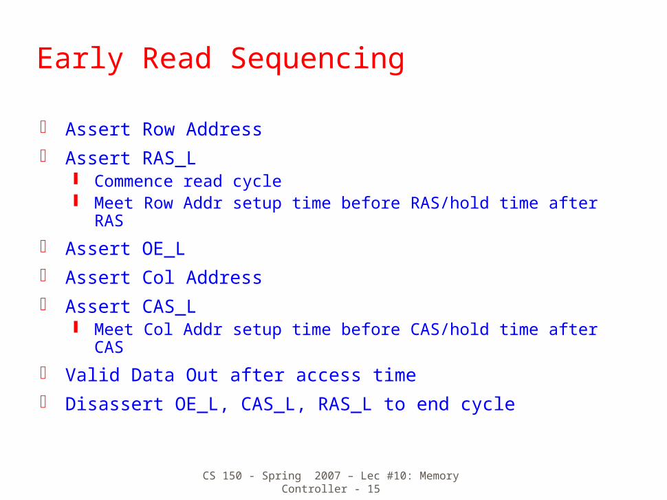
Early Read Sequencing
Assert Row Address Assert RAS_L
Commence read cycle Meet Row Addr setup time before RAS/hold time after RAS
Assert OE_L Assert Col Address Assert CAS_L
Meet Col Addr setup time before CAS/hold time after CAS
Valid Data Out after access time Disassert OE_L, CAS_L, RAS_L to end cycle
CS 150 - Spring 2007 – Lec #10: Memory Controller - 16
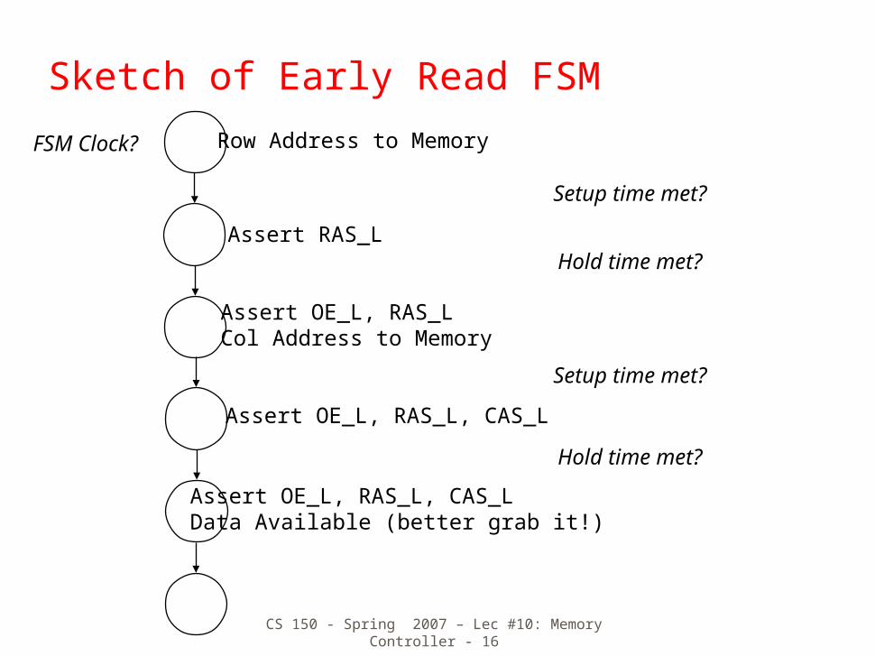
Sketch of Early Read FSM
Row Address to Memory
Assert RAS_L
Setup time met?
FSM Clock?
Assert OE_L, RAS_LCol Address to Memory
Hold time met?
Assert OE_L, RAS_L, CAS_L
Setup time met?
Hold time met?
Assert OE_L, RAS_L, CAS_LData Available (better grab it!)
CS 150 - Spring 2007 – Lec #10: Memory Controller - 17
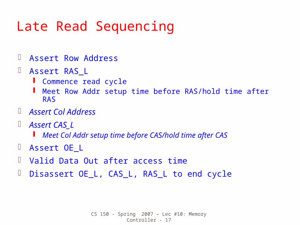
Late Read Sequencing
Assert Row Address Assert RAS_L
Commence read cycle Meet Row Addr setup time before RAS/hold time after RAS
Assert Col Address Assert CAS_L
Meet Col Addr setup time before CAS/hold time after CAS
Assert OE_L Valid Data Out after access time Disassert OE_L, CAS_L, RAS_L to end cycle
CS 150 - Spring 2007 – Lec #10: Memory Controller - 18
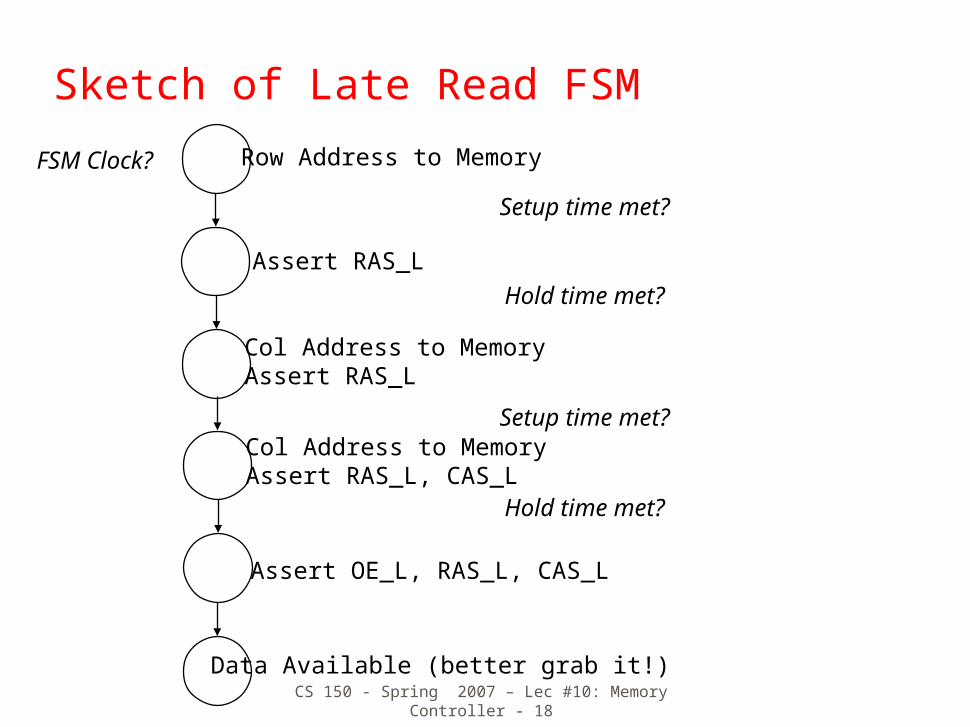
Sketch of Late Read FSM
Row Address to Memory
Assert RAS_L
Setup time met?
FSM Clock?
Col Address to MemoryAssert RAS_L
Hold time met?
Col Address to MemoryAssert RAS_L, CAS_L
Setup time met?
Hold time met?
Assert OE_L, RAS_L, CAS_L
Data Available (better grab it!)
CS 150 - Spring 2007 – Lec #10: Memory Controller - 19
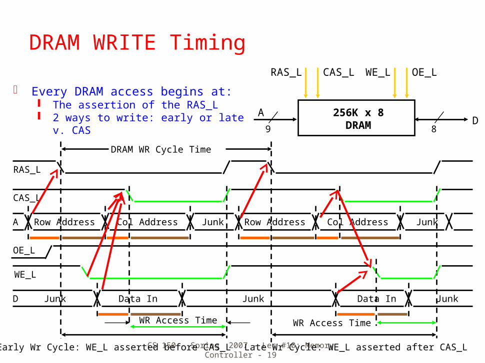
AD
OE_L
256K x 8DRAM9 8
WE_LCAS_LRAS_L
WE_L
A Row Address
OE_L
Junk
WR Access Time WR Access Time
CAS_L
RAS_L
Col Address Row Address JunkCol Address
D Junk JunkData In Data In Junk
DRAM WR Cycle Time
Early Wr Cycle: WE_L asserted before CAS_L Late Wr Cycle: WE_L asserted after CAS_L
Every DRAM access begins at: The assertion of the RAS_L 2 ways to write: early or late v. CAS
DRAM WRITE Timing
CS 150 - Spring 2007 – Lec #10: Memory Controller - 20
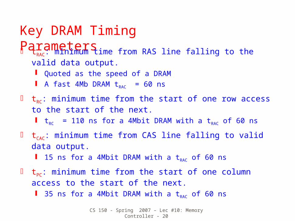
Key DRAM Timing Parameters tRAC: minimum time from RAS line falling to the valid data
output. Quoted as the speed of a DRAM A fast 4Mb DRAM tRAC = 60 ns
tRC: minimum time from the start of one row access to the start of the next. tRC = 110 ns for a 4Mbit DRAM with a tRAC of 60 ns
tCAC: minimum time from CAS line falling to valid data output. 15 ns for a 4Mbit DRAM with a tRAC of 60 ns
tPC: minimum time from the start of one column access to the start of the next. 35 ns for a 4Mbit DRAM with a tRAC of 60 ns

CS 150 - Spring 2007 – Lec #10: Memory Controller - 22
SDRAM Memory Controller
Static RAM Technology 6T Memory Cell Memory Access Timing
Dynamic RAM Technology 1T Memory Cell Memory Access Timing

![DESIGN OF 32-BIT MICROCONTROLLER … has 32-bit RICS microprocessor, data cache, instruction cache, FLASH controller, SDRAM controller, DMA (dynamic memory access), UART [7] (universal](https://img.pdfslide.us/doc/110x75/5adcdd157f8b9a9d4d8c5818/design-of-32-bit-microcontroller-has-32-bit-rics-microprocessor-data-cache.jpg)
![SDR SDRAM Controller For Real Time Data Processing · multiplexing. SRAM has disadvantages of low Memory density and expensive [1]. DRAMs are the main memory of all computing systems](https://img.pdfslide.us/doc/110x75/5e60a079ed81a46628251aca/sdr-sdram-controller-for-real-time-data-multiplexing-sram-has-disadvantages-of.jpg)