Embed Size (px)
Citation preview

SN74AHC595 . . . D, DB, N, NS, OR PW PACKAGE
(TOP VIEW)
SN54AHC595 . . . FK PACKAGE
(TOP VIEW)
NC − No internal connection
1
2
3
4
5
6
7
8
16
15
14
13
12
11
10
9
B
C
D
E
F
G
H
Q
Q
Q
Q
Q
Q
Q
GND
VCC
Q
SER
A
OE
RCLK
SRCLK
SRCLR
QH′
3 2 1 20 19
9 10 11 12 13
4
5
6
7
8
18
17
16
15
14
SER
OE
NC
RCLK
SRCLK
Q
Q
NC
D
E
Q
Q
F
G
Q NC
SR
CLRH
GN
D
NC
C
QB
VC
C
QA
Q
HQ
′
SN54AHC595 . . . J OR W PACKAGE
SN54AHC595, SN74AHC595
www.ti.com SCLS373J –MAY 1996–REVISED JULY 2013
8-BIT SHIFT REGISTERS WITH 3-STATE OUTPUT REGISTERSCheck for Samples: SN54AHC595, SN74AHC595
1FEATURES DESCRIPTIONThe ’AHC595 devices contain an 8-bit serial-in,• Operating Range 2-V to 5.5-V VCC parallel-out shift register that feeds an 8-bit D-type• 8-Bit Serial-In, Parallel-Out Shift storage register. The storage register has parallel 3-
• Latch-Up Performance Exceeds 100 mA Per state outputs. Separate clocks are provided for bothJESD 78, Class II the shift and storage registers. The shift register has
a direct overriding clear (SRCLR) input, serial (SER)• ESD Protection Exceeds JESD 22input, and a serial output for cascading. When the– 2000-V Human-Body Model (A114-A) output-enable (OE) input is high, all outputs, except
– 200-V Machine Model (A115-A) QH′, are in the high-impedance state.– 1000-V Charged-Device Model (C101) Both the shift-register clock (SRCLK) and storage-
register clock (RCLK) are positive-edge triggered. Ifboth clocks are connected together, the shift registeralways is one clock pulse ahead of the storageregister.
1
Please be aware that an important notice concerning availability, standard warranty, and use in critical applications ofTexas Instruments semiconductor products and disclaimers thereto appears at the end of this data sheet.
PRODUCTION DATA information is current as of publication date. Copyright © 1996–2013, Texas Instruments IncorporatedProducts conform to specifications per the terms of the TexasInstruments standard warranty. Production processing does notnecessarily include testing of all parameters.
SN54AHC595, SN74AHC595
SCLS373J –MAY 1996–REVISED JULY 2013 www.ti.com
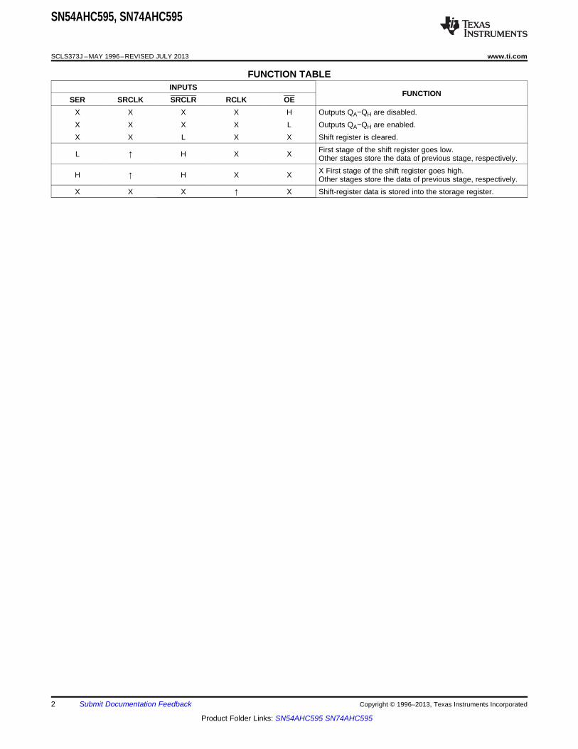
FUNCTION TABLEINPUTS
FUNCTIONSER SRCLK SRCLR RCLK OE
X X X X H Outputs QA−QH are disabled.X X X X L Outputs QA−QH are enabled.X X L X X Shift register is cleared.
First stage of the shift register goes low.L ↑ H X X Other stages store the data of previous stage, respectively.X First stage of the shift register goes high.H ↑ H X X Other stages store the data of previous stage, respectively.
X X X ↑ X Shift-register data is stored into the storage register.
2 Submit Documentation Feedback Copyright © 1996–2013, Texas Instruments Incorporated
Product Folder Links: SN54AHC595 SN74AHC595

3D
C3
1D
C1
R
3D
C3
2D
C2
R
3D
C3
2D
C2
R
3D
C3
2D
C2
R
3D
C3
2D
C2
R
3D
C3
2D
C2
R
3D
C3
2D
C2
R
3D
C3
2D
C2
R
13
12
10
11
14
15
1
2
3
4
5
6
7
9
QA
QB
QC
QD
QE
QF
QG
QH
QH′
OE
SRCLR
RCLK
SRCLK
SER Q
Q
Q
Q
Q
Q
Q
Q
Q
Q
Q
Q
Q
Q
Q
Q
SN54AHC595, SN74AHC595
www.ti.com SCLS373J –MAY 1996–REVISED JULY 2013
LOGIC DIAGRAM (POSITIVE LOGIC)
Pin numbers shown are for the D, DB, J, N, NS, PW, and W packages.
Copyright © 1996–2013, Texas Instruments Incorporated Submit Documentation Feedback 3
Product Folder Links: SN54AHC595 SN74AHC595

SRCLK
SER
RCLK
SRCLR
OE
QA
QB
QC
QD
QE
QF
QG
QH
QH′
implies that the output is in 3-State mode.NOTE:
SN54AHC595, SN74AHC595
SCLS373J –MAY 1996–REVISED JULY 2013 www.ti.com
TIMING DIAGRAM
4 Submit Documentation Feedback Copyright © 1996–2013, Texas Instruments Incorporated
Product Folder Links: SN54AHC595 SN74AHC595

SN54AHC595, SN74AHC595
www.ti.com SCLS373J –MAY 1996–REVISED JULY 2013
ABSOLUTE MAXIMUM RATINGSover operating free-air temperature range (unless otherwise noted) (1)
VALUE UNITSupply voltage range, VCC –0.5 to 7 VInput voltage range, VI
(2) –0.5 to 7 VOutput voltage range, VO
(2) –0.5 to VCC + 0.5 VInput clamp current, IIK (VI < 0) –20 mAOutput clamp current, IOK (VO < 0 or VO > VCC) ±20 mAContinuous output current, IO (VO = 0 to VCC) ±25 mAContinuous current through VCC or GND ±75 mA
D package (3) 73DB package (3) 82
Package thermal impedance, θJA N package (3) 67 °C/WNS package (3) 64PW package (3) 108
Storage temperature range, Tstg –65 to 150 °C
(1) Stresses beyond those listed under “absolute maximum ratings” may cause permanent damage to the device. These are stress ratingsonly, and functional operation of the device at these or any other conditions beyond those indicated under “recommended operatingconditions” is not implied. Exposure to absolute-maximum-rated conditions for extended periods may affect device reliability.
(2) The input and output voltage ratings may be exceeded if the input and output current ratings are observed.(3) The package thermal impedance is calculated in accordance with JESD 51-7.
RECOMMENDED OPERATING CONDITIONS (1)
SN54AHC595 (2) SN74AHC595UNIT
MIN MAX MIN MAXVCC Supply voltage 2 5.5 2 5.5 V
VCC= 2 V 1.5 1.5VIH High-level input voltage VCC= 3V 2.1 2.1 V
VCC= 5.5 V 3.85 3.85VCC= 2 V 0.5 0.5
VIL Low-level Input voltage VCC= 3 V 0.9 0.9 VVCC= 5.5 V 1.65 1.65
VI Input voltage 0 5.5 0 5.5 VVO Output voltage 0 VCC 0 VCC V
VCC= 2 V –50 –50IOH High-level output current VCC= 3.3 V ± 0.3 V –4 –4 mA
VCC= 5 V ± 0.5 V –8 –8VCC= 2 V 50 50
IOL Low-level output current VCC= 3.3 V ± 0.3 V 4 4 mAVCC= 5 V ± 0.5 V 8 8VCC= 3.3 V ± 0.3 V 100 100
Δt/Δv Input Transition rise or fall rate ns/VVCC= 5 V ± 0.5 V 20 20
TA Operating free-air temperature –55 125 –40 125 °C
(1) All unused inputs of the device must be held at VCC or GND to ensure proper device operation. Refer to the TI application report,Implications of Slow or Floating CMOS Inputs, literature number SCBA004.
(2) Product Preview.
Copyright © 1996–2013, Texas Instruments Incorporated Submit Documentation Feedback 5
Product Folder Links: SN54AHC595 SN74AHC595

SN54AHC595, SN74AHC595
SCLS373J –MAY 1996–REVISED JULY 2013 www.ti.com
ELECTRICAL CHARACTERISTICSover operating free-air temperature range (unless otherwise noted)
–40°C TO 125°C–55°C TO 125°C –40°C TO 85°CTA = 25°C RecommendedSN54AHC595 (1) SN74AHC595PARAMETER TEST CONDITIONS VCC UNITSN74AHC595
MIN TYP MAX MIN MAX MIN MAX MIN MAX
2 V 1.9 2 1.9 1.9 1.9
IOH = –50 µA 3 V 2.9 3 2.9 2.9 2.9
VOH 4.5 V 4.4 4.5 4.4 4.4 4.4 V
IOH = –4 mA 3 V 2.58 2.48 2.48 2.48
IOH = –8 mA 4.5 V 3.94 3.8 3.8 3.8
2 V 0.1 0.1 0.1 0.1
IOL = 50 µA 3 V 0.1 0.1 0.1 0.1
VOL 4.5 V 0.1 0.1 0.1 0.1 V
IOH = 4 mA 3 V 0.36 0.5 0.44 0.44
IOH = 8 mA 4.5 V 0.36 0.5 0.44 0.44
0 V to 5.5II VI = 5.5 V or GND ±0.1 ±1 (2) ±1 ±1 µAV
VI = VCC orGND,VO = VCC or QA –IOZ 5.5 V ±0.25 ±2.5 ±2.5 ±2.5GND, QHOE = VIH orVIL,
VI = VCC orICC IO = 0 5.5 V 4 40 40 40 µAGND,
Ci VI = VCC or GND 5 V 3 10 10 pF
CO VO = VCC or GND, 5 V 5.5
(1) Product Preview.(2) On products compliant to MIL-PRF-38535, this parameter is not production tested at VCC = 0 V.
TIMING REQUIREMENTSover recommended operating free-air temperature range, VCC = 3.3 V ± 0.3 V (unless otherwise noted) (see Figure 1)
–40°C TO 125°C–55°C TO 125°C –40°C TO 85°CTA = 25°C RecommendedSN54AHC595 (1) SN74AHC595 UNITSN74AHC595
MIN MAX MIN MAX MIN MAX MIN MAX
SRCLK high or low 5 5 5 6
tW Pulse duration RCLK high or low 5 5 5 6 ns
SRCLR low 5 5 5 6.5
SER before SRCLK↑ 3.5 3.5 3.5 4.5
SRCLK↑ before RCLK↑ (2) 8 8.5 8.5 9.5tsu Setup time nsSRCLR low before RCLK↑ 8 9 9 10
SRCLR high (inactive) before 3 3 3 4SRCLK↑
th Hold time SER after SRCLK↑ 1.5 1.5 1.5 2.5 ns
(1) Product Preview.(2) This setup time allows the storage register to receive stable data from the shift register. The clocks can be tied together, in which case
the shift register is one clock pulse ahead of the storage register.
6 Submit Documentation Feedback Copyright © 1996–2013, Texas Instruments Incorporated
Product Folder Links: SN54AHC595 SN74AHC595

SN54AHC595, SN74AHC595
www.ti.com SCLS373J –MAY 1996–REVISED JULY 2013
TIMING REQUIREMENTSover recommended operating free-air temperature range, VCC = 5 V ± 0.5 V (unless otherwise noted) (see Figure 1)
–40°C TO 125°C–55°C TO 125°C –40°C TO 85°CTA = 25°C RecommendedSN54AHC595 (1) SN74AHC595 UNITSN74AHC595
MIN MAX MIN MAX MIN MAX MIN MAX
SRCLK high or low 5 5 5 6
tW Pulse duration RCLK high or low 5 5 5 6 ns
SRCLR low 5 5 5 6.2
SER before SRCLK↑ 3 3 3 4
SRCLK↑ before RCLK↑ (2) 5 5 5 6tsu Setup time nsSRCLR low before RCLK↑ 5 5 5 6
SRCLR high (inactive) before 2.5 2.5 2.5 3.5SRCLK↑
th Hold time SER after SRCLK↑ 2 2 2 3 ns
(1) Product Preview.(2) This setup time allows the storage register to receive stable data from the shift register. The clocks can be tied together, in which case
the shift register is one clock pulse ahead of the storage register.
SWITCHING CHARACTERISTICSover recommended operating free-air temperature range, VCC = 3.3 V ± 0.3 V (unless otherwise noted) (see Figure 1)
–55°C TO –40°C TO –40°C TO 125°CLOAD TA = 25°C 125°C 85°C RecommendedFROM TOPARAMETER CAPACITANC UNITSN54AHC595 SN74AHC595 SN74AHC595(INPUT) (OUTPUT) E
MIN TYP MAX MIN MAX MIN MAX MIN MAX
CL = 15 pF 80 (1) 120 (1) 70 (1) 70 60fmax MHz
CL = 50 pF 55 105 50 50 40
13.5 (1tPLH 6 (1) 11.9 (1) 1 (1) 1 13.5 1 14.9)
RCLK QA – QH CL = 15 pF ns13.5 (1
tPHL 6 (1) 11.9 (1) 1 (1) 1 13.5 1 14.9)
tPLH 6.6 (1) 13 (1) 1 (1) 15 (1) 1 15 1 16.4SRCLK QH' CL = 15 pF ns
tPHL 6.6 (1) 13 (1) 1 (1) 15 (1) 1 15 1 16.4
13.7 (1tPHL SRCLR QH' CL = 15 pF 6.2 (1) 12.8 (1) 1 (1) 1 13.7 1 15 ns)
13.5 (1tPZH 6 (1) 11.5 (1) 1 (1) 1 13.5 1 14.9)
OE QA – QH CL = 15 pF ns13.5 (1
tPZL 7.8 (1) 11.5 (1) 1 (1) 1 13.5 1 14.9)
tPLH 7.9 15.4 1 17 1 17 1 18.6RCLK QA – QH CL = 50 pF ns
tPHL 7.9 15.4 1 17 1 17 1 18.6
tPLH 9.2 16.5 1 18.5 1 18.5 1 20SRCLK QH' CL = 50 pF ns
tPHL 9.2 16.5 1 18.5 1 18.5 1 20
tPHL SRCLR QH' CL = 50 pF 9 16.3 1 17.2 1 17.2 1 18.7 ns
tPZH 7.8 15 1 17 1 17 1 18.6OE QA – QH CL = 50 pF ns
tPZL 9.6 15 1 17 1 17 1 18.6
tPHZ 8.1 15.7 1 16.2 1 16.2 1 17.4OE QA – QH CL = 50 pF ns
tPLZ 9.3 15.7 1 16.2 1 16.2 1 17.4
(1) On products compliant to MIL-PRF-38535, this parameter is not production tested.
Copyright © 1996–2013, Texas Instruments Incorporated Submit Documentation Feedback 7
Product Folder Links: SN54AHC595 SN74AHC595

SN54AHC595, SN74AHC595
SCLS373J –MAY 1996–REVISED JULY 2013 www.ti.com
SWITCHING CHARACTERISTICSover recommended operating free-air temperature range, VCC = 5 V ± 0.5 V (unless otherwise noted) (see Figure 1)
–55°C TO 125°C –40°C TO 85°CTA = 25°CFROM TO LOAD SN54AHC595 SN74AHC595PARAMETER UNIT(INPUT) (OUTPUT) CAPACITANCEMIN TYP MAX MIN MAX MIN MAX
CL = 15 pF 135 (1) 170 (1) 115 (1) 115fmax MHz
CL = 50 pF 95 140 85 85
tPLH 4.3 (1) 7.4 (1) 1 (1) 8.5 (1) 1 8.5RCLK QA – QH CL = 15 pF ns
tPHL 4.3 (1) 7.4 (1) 1 (1) 8.5 (1) 1 8.5
tPLH 4.5 (1) 8.2 (1) 1 (1) 9.4 (1) 1 9.4SRCLK QH' CL = 15 pF ns
tPHL 4.5 (1) 8.2 (1) 1 (1) 9.4 (1) 1 9.4
tPHL SRCLR QH' CL = 15 pF 4.5 (1) 8 (1) 1 (1) 9.1 (1) 1 9.1 ns
tPZH 4.3 (1) 8.6 (1) 1 (1) 10 (1) 1 10OE QA – QH CL = 15 pF ns
tPZL 5.4 (1) 8.6 (1) 1 (1) 10 (1) 1 10
tPLH 5.6 9.4 1 10.5 1 10.5RCLK QA – QH CL = 50 pF ns
tPHL 5.6 9.4 1 10.5 1 10.5
tPLH 6.4 10.2 1 11.4 1 11.4SRCLK QH' CL = 50 pF ns
tPHL 6.4 10.2 1 11.4 1 11.4
tPHL SRCLR QH' CL = 50 pF 6.4 10 1 11.1 1 11.1 ns
tPZH 5.7 10.6 1 12 1 12OE QA – QH CL = 50 pF ns
tPZL 6.8 10.6 1 12 1 12
tPHZ 3.5 10.3 1 11 1 11OE QA – QH CL = 50 pF ns
tPLZ 3.4 10.3 1 11 1 11
(1) On products compliant to MIL-PRF-38535, this parameter is not production tested.
OPERATING CHARACTERISTICSVCC = 5 V, TA = 25°C
PARAMETER TEST CONDITIONS TYP UNITCpd Power dissipation capacitance No load, f = 1 MHz 25.2 pF
8 Submit Documentation Feedback Copyright © 1996–2013, Texas Instruments Incorporated
Product Folder Links: SN54AHC595 SN74AHC595

50% VCC
VCC
VCC
0 V
0 V
thtsu
VOLTAGE WAVEFORMS
SETUP AND HOLD TIMES
Data Input
tPLH
tPHL
tPHL
tPLH
VOH
VOH
VOL
VOL
VCC
0 V
50% VCC50% VCC
Input
Out-of-Phase
Output
In-Phase
Output
Timing Input
50% VCC
VOLTAGE WAVEFORMS
PROPAGATION DELAY TIMES
INVERTING AND NONINVERTING OUTPUTS
Output
Control
Output
Waveform 1
S1 at VCC(see Note B)
Output
Waveform 2
S1 at GND
(see Note B)
VOL
VOH
tPZL
tPZH
tPLZ
tPHZ
≈VCC
0 V
50% VCC VOL + 0.3 V
50% VCC≈0 V
VCC
VOLTAGE WAVEFORMS
ENABLE AND DISABLE TIMES
LOW- AND HIGH-LEVEL ENABLING
tPLH/tPHLtPLZ/tPZLtPHZ/tPZHOpen Drain
Open
VCCGND
VCC
TEST S1
VCC
0 V
50% VCC
tw
VOLTAGE WAVEFORMS
PULSE DURATION
Input
From Output
Under Test
CL(see Note A)
LOAD CIRCUIT FOR
3-STATE AND OPEN-DRAIN OUTPUTS
S1
VCC
RL = 1 kΩ
GNDFrom Output
Under Test
CL(see Note A)
Test
Point
LOAD CIRCUIT FOR
TOTEM-POLE OUTPUTS
Open
50% VCC
50% VCC 50% VCC
50% VCC
50% VCC 50% VCC
50% VCC 50% VCC
VOH – 0.3 V
SN54AHC595, SN74AHC595
www.ti.com SCLS373J –MAY 1996–REVISED JULY 2013
PARAMETER MEASUREMENT INFORMATION
A. CL includes probe and jig capacitance.B. Waveform 1 is for an output with internal conditions such that the output is low except when disabled by the output
control.Waveform 2 is for an output with internal conditions such that the output is high except when disabled by the outputcontrol.
C. All input pulses are supplied by generators having the following characteristics: PRR ≤ 1 MHz, ZO = 50 Ω, tr ≤ 3 ns, tf≤ 3 ns.
D. The outputs are measured one at a time with one input transition per measurement.E. All parameters and waveforms are not applicable to all devices.
Figure 1. Load Circuit and Voltage Waveforms
Copyright © 1996–2013, Texas Instruments Incorporated Submit Documentation Feedback 9
Product Folder Links: SN54AHC595 SN74AHC595

SN54AHC595, SN74AHC595
SCLS373J –MAY 1996–REVISED JULY 2013 www.ti.com
REVISION HISTORY
Changes from Revision I (June 2004) to Revision J Page
• Changed Updated document to new TI datasheet format. ................................................................................................... 1• Extended operating temperature range to 125°C ................................................................................................................. 5
10 Submit Documentation Feedback Copyright © 1996–2013, Texas Instruments Incorporated
Product Folder Links: SN54AHC595 SN74AHC595
PACKAGE OPTION ADDENDUM
www.ti.com 18-Oct-2013
Addendum-Page 1
PACKAGING INFORMATION
Orderable Device Status(1)
Package Type PackageDrawing
Pins PackageQty
Eco Plan(2)
Lead/Ball Finish(6)
MSL Peak Temp(3)
Op Temp (°C) Device Marking(4/5)
Samples
SN74AHC595D ACTIVE SOIC D 16 40 Green (RoHS& no Sb/Br)
CU NIPDAU Level-1-260C-UNLIM -40 to 125 AHC595
SN74AHC595DBR ACTIVE SSOP DB 16 2000 Green (RoHS& no Sb/Br)
CU NIPDAU Level-1-260C-UNLIM -40 to 125 HA595
SN74AHC595DBRE4 ACTIVE SSOP DB 16 2000 Green (RoHS& no Sb/Br)
CU NIPDAU Level-1-260C-UNLIM -40 to 125 HA595
SN74AHC595DBRG4 ACTIVE SSOP DB 16 2000 Green (RoHS& no Sb/Br)
CU NIPDAU Level-1-260C-UNLIM -40 to 125 HA595
SN74AHC595DE4 ACTIVE SOIC D 16 40 Green (RoHS& no Sb/Br)
CU NIPDAU Level-1-260C-UNLIM -40 to 125 AHC595
SN74AHC595DG4 ACTIVE SOIC D 16 40 Green (RoHS& no Sb/Br)
CU NIPDAU Level-1-260C-UNLIM -40 to 125 AHC595
SN74AHC595DR ACTIVE SOIC D 16 2500 Green (RoHS& no Sb/Br)
CU NIPDAU Level-1-260C-UNLIM -40 to 125 AHC595
SN74AHC595DRE4 ACTIVE SOIC D 16 2500 Green (RoHS& no Sb/Br)
CU NIPDAU Level-1-260C-UNLIM -40 to 125 AHC595
SN74AHC595DRG4 ACTIVE SOIC D 16 2500 Green (RoHS& no Sb/Br)
CU NIPDAU Level-1-260C-UNLIM -40 to 125 AHC595
SN74AHC595N ACTIVE PDIP N 16 25 Pb-Free(RoHS)
CU NIPDAU N / A for Pkg Type -40 to 125 SN74AHC595N
SN74AHC595NE4 ACTIVE PDIP N 16 25 Pb-Free(RoHS)
CU NIPDAU N / A for Pkg Type -40 to 125 SN74AHC595N
SN74AHC595PW ACTIVE TSSOP PW 16 90 Green (RoHS& no Sb/Br)
CU NIPDAU Level-1-260C-UNLIM -40 to 125 HA595
SN74AHC595PWE4 ACTIVE TSSOP PW 16 90 Green (RoHS& no Sb/Br)
CU NIPDAU Level-1-260C-UNLIM -40 to 125 HA595
SN74AHC595PWG4 ACTIVE TSSOP PW 16 90 Green (RoHS& no Sb/Br)
CU NIPDAU Level-1-260C-UNLIM -40 to 125 HA595
SN74AHC595PWR ACTIVE TSSOP PW 16 2000 Green (RoHS& no Sb/Br)
CU NIPDAU | CU SN Level-1-260C-UNLIM -40 to 125 HA595
SN74AHC595PWRE4 ACTIVE TSSOP PW 16 2000 Green (RoHS& no Sb/Br)
CU NIPDAU Level-1-260C-UNLIM -40 to 125 HA595
SN74AHC595PWRG4 ACTIVE TSSOP PW 16 2000 Green (RoHS& no Sb/Br)
CU NIPDAU Level-1-260C-UNLIM -40 to 125 HA595
PACKAGE OPTION ADDENDUM
www.ti.com 18-Oct-2013
Addendum-Page 2
(1) The marketing status values are defined as follows:ACTIVE: Product device recommended for new designs.LIFEBUY: TI has announced that the device will be discontinued, and a lifetime-buy period is in effect.NRND: Not recommended for new designs. Device is in production to support existing customers, but TI does not recommend using this part in a new design.PREVIEW: Device has been announced but is not in production. Samples may or may not be available.OBSOLETE: TI has discontinued the production of the device.
(2) Eco Plan - The planned eco-friendly classification: Pb-Free (RoHS), Pb-Free (RoHS Exempt), or Green (RoHS & no Sb/Br) - please check http://www.ti.com/productcontent for the latest availabilityinformation and additional product content details.TBD: The Pb-Free/Green conversion plan has not been defined.Pb-Free (RoHS): TI's terms "Lead-Free" or "Pb-Free" mean semiconductor products that are compatible with the current RoHS requirements for all 6 substances, including the requirement thatlead not exceed 0.1% by weight in homogeneous materials. Where designed to be soldered at high temperatures, TI Pb-Free products are suitable for use in specified lead-free processes.Pb-Free (RoHS Exempt): This component has a RoHS exemption for either 1) lead-based flip-chip solder bumps used between the die and package, or 2) lead-based die adhesive used betweenthe die and leadframe. The component is otherwise considered Pb-Free (RoHS compatible) as defined above.Green (RoHS & no Sb/Br): TI defines "Green" to mean Pb-Free (RoHS compatible), and free of Bromine (Br) and Antimony (Sb) based flame retardants (Br or Sb do not exceed 0.1% by weightin homogeneous material)
(3) MSL, Peak Temp. - The Moisture Sensitivity Level rating according to the JEDEC industry standard classifications, and peak solder temperature.
(4) There may be additional marking, which relates to the logo, the lot trace code information, or the environmental category on the device.
(5) Multiple Device Markings will be inside parentheses. Only one Device Marking contained in parentheses and separated by a "~" will appear on a device. If a line is indented then it is a continuationof the previous line and the two combined represent the entire Device Marking for that device.
(6) Lead/Ball Finish - Orderable Devices may have multiple material finish options. Finish options are separated by a vertical ruled line. Lead/Ball Finish values may wrap to two lines if the finishvalue exceeds the maximum column width.
Important Information and Disclaimer:The information provided on this page represents TI's knowledge and belief as of the date that it is provided. TI bases its knowledge and belief on informationprovided by third parties, and makes no representation or warranty as to the accuracy of such information. Efforts are underway to better integrate information from third parties. TI has taken andcontinues to take reasonable steps to provide representative and accurate information but may not have conducted destructive testing or chemical analysis on incoming materials and chemicals.TI and TI suppliers consider certain information to be proprietary, and thus CAS numbers and other limited information may not be available for release.
In no event shall TI's liability arising out of such information exceed the total purchase price of the TI part(s) at issue in this document sold by TI to Customer on an annual basis.
OTHER QUALIFIED VERSIONS OF SN74AHC595 :
• Automotive: SN74AHC595-Q1

PACKAGE OPTION ADDENDUM
www.ti.com 18-Oct-2013
Addendum-Page 3
NOTE: Qualified Version Definitions:
• Automotive - Q100 devices qualified for high-reliability automotive applications targeting zero defects

TAPE AND REEL INFORMATION
*All dimensions are nominal
Device PackageType
PackageDrawing
Pins SPQ ReelDiameter
(mm)
ReelWidth
W1 (mm)
A0(mm)
B0(mm)
K0(mm)
P1(mm)
W(mm)
Pin1Quadrant
SN74AHC595DBR SSOP DB 16 2000 330.0 16.4 8.2 6.6 2.5 12.0 16.0 Q1
SN74AHC595DR SOIC D 16 2500 330.0 16.4 6.5 10.3 2.1 8.0 16.0 Q1
SN74AHC595PWR TSSOP PW 16 2000 330.0 12.4 6.9 5.6 1.6 8.0 12.0 Q1
SN74AHC595PWR TSSOP PW 16 2000 330.0 12.4 7.0 5.6 1.6 8.0 12.0 Q1
SN74AHC595PWRG4 TSSOP PW 16 2000 330.0 12.4 6.9 5.6 1.6 8.0 12.0 Q1
PACKAGE MATERIALS INFORMATION
www.ti.com 1-Aug-2013
Pack Materials-Page 1

*All dimensions are nominal
Device Package Type Package Drawing Pins SPQ Length (mm) Width (mm) Height (mm)
SN74AHC595DBR SSOP DB 16 2000 367.0 367.0 38.0
SN74AHC595DR SOIC D 16 2500 367.0 367.0 38.0
SN74AHC595PWR TSSOP PW 16 2000 367.0 367.0 35.0
SN74AHC595PWR TSSOP PW 16 2000 364.0 364.0 27.0
SN74AHC595PWRG4 TSSOP PW 16 2000 367.0 367.0 35.0
PACKAGE MATERIALS INFORMATION
www.ti.com 1-Aug-2013
Pack Materials-Page 2


MECHANICAL DATA
MSSO002E – JANUARY 1995 – REVISED DECEMBER 2001
POST OFFICE BOX 655303 • DALLAS, TEXAS 75265
DB (R-PDSO-G**) PLASTIC SMALL-OUTLINE
4040065 /E 12/01
28 PINS SHOWN
Gage Plane
8,207,40
0,550,95
0,25
38
12,90
12,30
28
10,50
24
8,50
Seating Plane
9,907,90
30
10,50
9,90
0,38
5,605,00
15
0,22
14
A
28
1
2016
6,506,50
14
0,05 MIN
5,905,90
DIM
A MAX
A MIN
PINS **
2,00 MAX
6,90
7,50
0,65 M0,15
0°–8°
0,10
0,090,25
NOTES: A. All linear dimensions are in millimeters.B. This drawing is subject to change without notice.C. Body dimensions do not include mold flash or protrusion not to exceed 0,15.D. Falls within JEDEC MO-150

IMPORTANT NOTICE
Texas Instruments Incorporated and its subsidiaries (TI) reserve the right to make corrections, enhancements, improvements and otherchanges to its semiconductor products and services per JESD46, latest issue, and to discontinue any product or service per JESD48, latestissue. Buyers should obtain the latest relevant information before placing orders and should verify that such information is current andcomplete. All semiconductor products (also referred to herein as “components”) are sold subject to TI’s terms and conditions of salesupplied at the time of order acknowledgment.
TI warrants performance of its components to the specifications applicable at the time of sale, in accordance with the warranty in TI’s termsand conditions of sale of semiconductor products. Testing and other quality control techniques are used to the extent TI deems necessaryto support this warranty. Except where mandated by applicable law, testing of all parameters of each component is not necessarilyperformed.
TI assumes no liability for applications assistance or the design of Buyers’ products. Buyers are responsible for their products andapplications using TI components. To minimize the risks associated with Buyers’ products and applications, Buyers should provideadequate design and operating safeguards.
TI does not warrant or represent that any license, either express or implied, is granted under any patent right, copyright, mask work right, orother intellectual property right relating to any combination, machine, or process in which TI components or services are used. Informationpublished by TI regarding third-party products or services does not constitute a license to use such products or services or a warranty orendorsement thereof. Use of such information may require a license from a third party under the patents or other intellectual property of thethird party, or a license from TI under the patents or other intellectual property of TI.
Reproduction of significant portions of TI information in TI data books or data sheets is permissible only if reproduction is without alterationand is accompanied by all associated warranties, conditions, limitations, and notices. TI is not responsible or liable for such altereddocumentation. Information of third parties may be subject to additional restrictions.
Resale of TI components or services with statements different from or beyond the parameters stated by TI for that component or servicevoids all express and any implied warranties for the associated TI component or service and is an unfair and deceptive business practice.TI is not responsible or liable for any such statements.
Buyer acknowledges and agrees that it is solely responsible for compliance with all legal, regulatory and safety-related requirementsconcerning its products, and any use of TI components in its applications, notwithstanding any applications-related information or supportthat may be provided by TI. Buyer represents and agrees that it has all the necessary expertise to create and implement safeguards whichanticipate dangerous consequences of failures, monitor failures and their consequences, lessen the likelihood of failures that might causeharm and take appropriate remedial actions. Buyer will fully indemnify TI and its representatives against any damages arising out of the useof any TI components in safety-critical applications.
In some cases, TI components may be promoted specifically to facilitate safety-related applications. With such components, TI’s goal is tohelp enable customers to design and create their own end-product solutions that meet applicable functional safety standards andrequirements. Nonetheless, such components are subject to these terms.
No TI components are authorized for use in FDA Class III (or similar life-critical medical equipment) unless authorized officers of the partieshave executed a special agreement specifically governing such use.
Only those TI components which TI has specifically designated as military grade or “enhanced plastic” are designed and intended for use inmilitary/aerospace applications or environments. Buyer acknowledges and agrees that any military or aerospace use of TI componentswhich have not been so designated is solely at the Buyer's risk, and that Buyer is solely responsible for compliance with all legal andregulatory requirements in connection with such use.
TI has specifically designated certain components as meeting ISO/TS16949 requirements, mainly for automotive use. In any case of use ofnon-designated products, TI will not be responsible for any failure to meet ISO/TS16949.
Products Applications
Audio www.ti.com/audio Automotive and Transportation www.ti.com/automotive
Amplifiers amplifier.ti.com Communications and Telecom www.ti.com/communications
Data Converters dataconverter.ti.com Computers and Peripherals www.ti.com/computers
DLP® Products www.dlp.com Consumer Electronics www.ti.com/consumer-apps
DSP dsp.ti.com Energy and Lighting www.ti.com/energy
Clocks and Timers www.ti.com/clocks Industrial www.ti.com/industrial
Interface interface.ti.com Medical www.ti.com/medical
Logic logic.ti.com Security www.ti.com/security
Power Mgmt power.ti.com Space, Avionics and Defense www.ti.com/space-avionics-defense
Microcontrollers microcontroller.ti.com Video and Imaging www.ti.com/video
RFID www.ti-rfid.com
OMAP Applications Processors www.ti.com/omap TI E2E Community e2e.ti.com
Wireless Connectivity www.ti.com/wirelessconnectivity
Mailing Address: Texas Instruments, Post Office Box 655303, Dallas, Texas 75265Copyright © 2013, Texas Instruments Incorporated

![BOOK EIGHT: ON PUBLIC FINANCE AND THE PUBLIC SERVICE … · IOIO!e-.-., ~(Q)~(Q)JfM (FREEDOM) No. 30/96 Thursday, 25 July, 1996 ISSN: 0796-0573 Price: D200 1 ill ;~~Q~~ (]J~ 1JOO~](https://img.pdfslide.us/doc/110x75/60b70f50e8095c6dae008973/book-eight-on-public-finance-and-the-public-service-ioioe-qqjfm-freedom.jpg)