Embed Size (px)
Citation preview

Chapter 2 – Digital Components Section 2.1 – Integrated Circuits
An integrated circuit (IC) is a small silicon semiconductor crystal, called a chip, containing the electronic components for the digital gates
The various gates are interconnected inside the chip to form the required circuit The chip is mounted in a ceramic or plastic container, and connections are welded
by thin gold wires to external pins to form the IC The number of pins range from 14 to 100 Each IC has a numeric designation Small-scale integration (SSI) – several independent gates in a single package
(usually < 10) Medium-scale integration (MSI) – approximately 10 to 200 gates – decoders,
adders, or registers Large-scale integration (LSI) – between 200 and a few thousand gates – memory
chips, processors, or programmable modules Very-large-scale integration (VLSI) – thousands of gates – large memory arrays
or complex microcomputer chips Digital integrated circuits are classified not only by their logic operations, but
also by their digital logic family o TTL Transistor-transistor logic (standard) o ECL Emitter-coupled logic o MOS Metal-oxide semiconductor o CMOS Complementary metal-oxide semiconductor
Section 2.2 – Decoders
A binary code of n bits is capable of representing up to 2n distinct elements of the coded information
A decoder is a combinational circuit that converts binary information from the n coded inputs to a maximum of 2n unique outputs
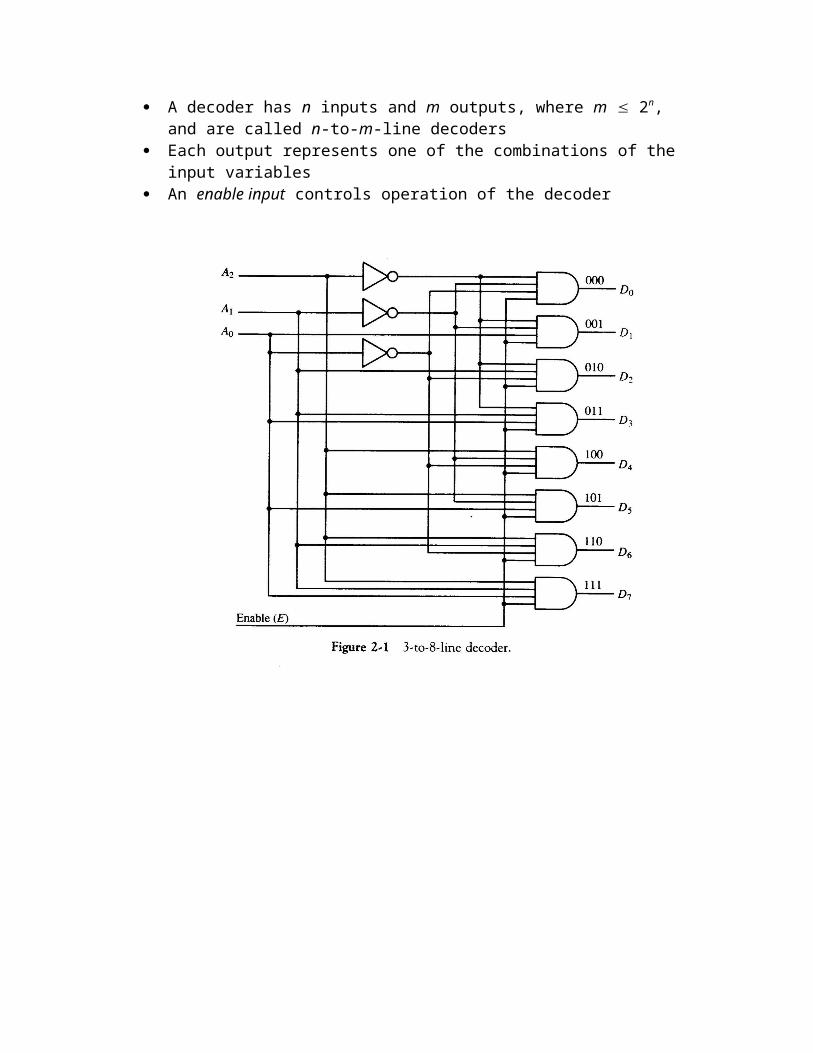
A decoder has n inputs and m outputs, where m £ 2n, and are called n-to-m-line decoders
Each output represents one of the combinations of the input variables An enable input controls operation of the decoder
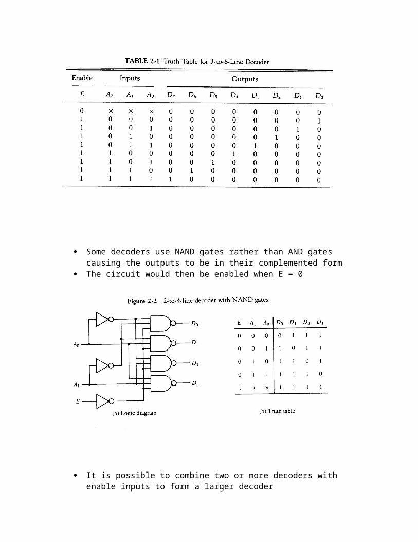
Some decoders use NAND gates rather than AND gates causing the outputs to be in their complemented form
The circuit would then be enabled when E = 0
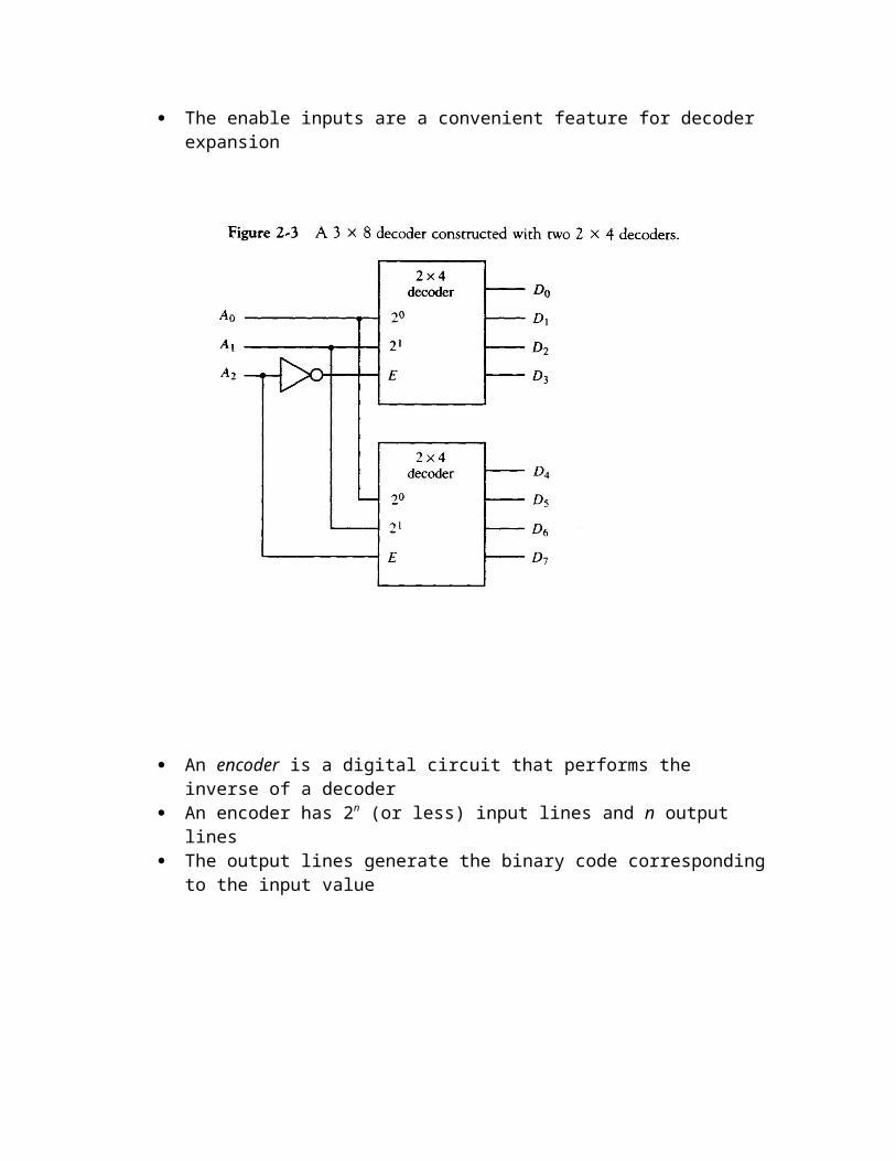
It is possible to combine two or more decoders with enable inputs to form a larger
decoder The enable inputs are a convenient feature for decoder expansion
An encoder is a digital circuit that performs the inverse of a decoder An encoder has 2n (or less) input lines and n output lines The output lines generate the binary code corresponding to the input value
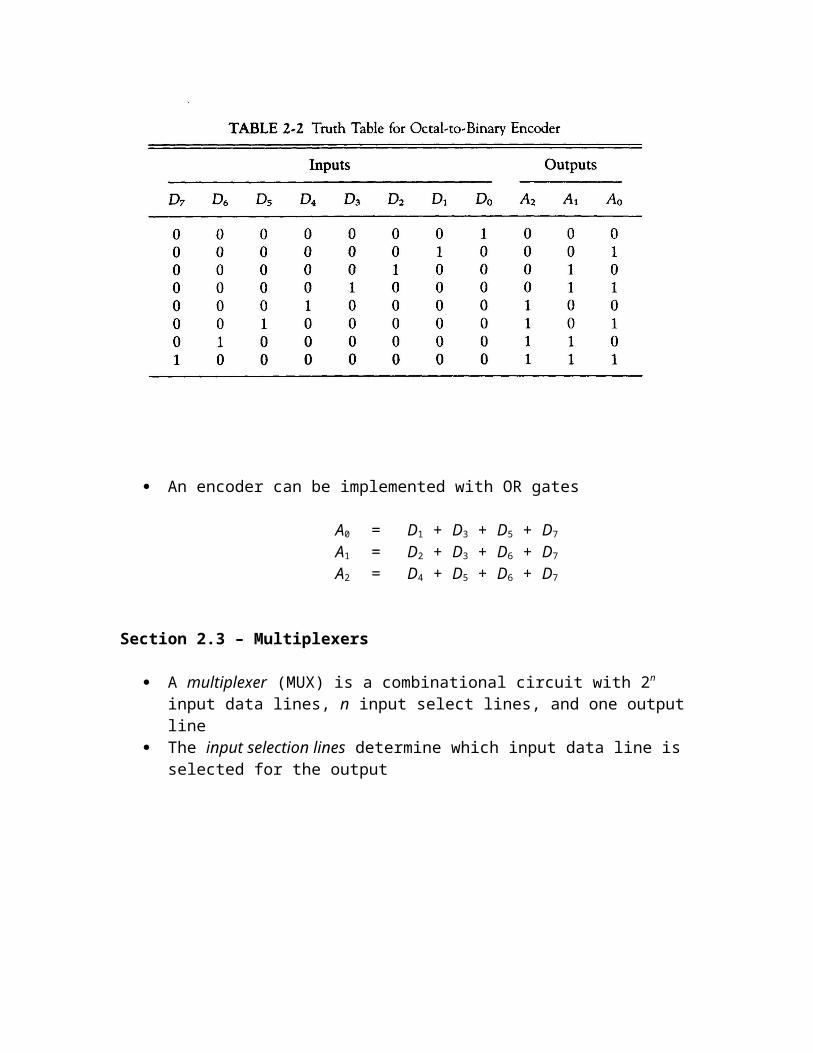
An encoder can be implemented with OR gates
A0 = D1 + D3 + D5 + D7
A1 = D2 + D3 + D6 + D7
A2 = D4 + D5 + D6 + D7
Section 2.3 – Multiplexers
A multiplexer (MUX) is a combinational circuit with 2n input data lines, n input select lines, and one output line
The input selection lines determine which input data line is selected for the output
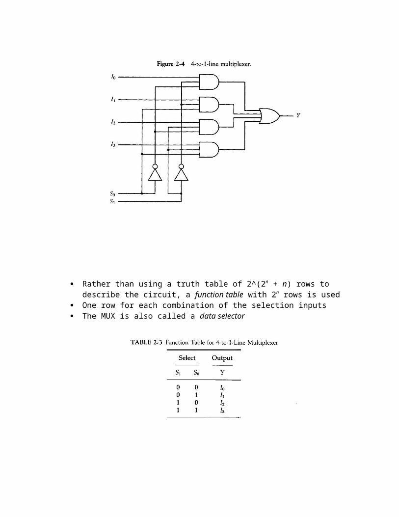
Rather than using a truth table of 2^(2n + n) rows to describe the circuit, a function
table with 2n rows is used One row for each combination of the selection inputs The MUX is also called a data selector
A 2n-to-1 line MUX is constructed from an n-to-2n decoder by adding to it 2n
input lines, one from each data input
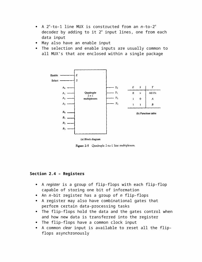
May also have an enable input The selection and enable inputs are usually common to all MUX’s that are
enclosed within a single package
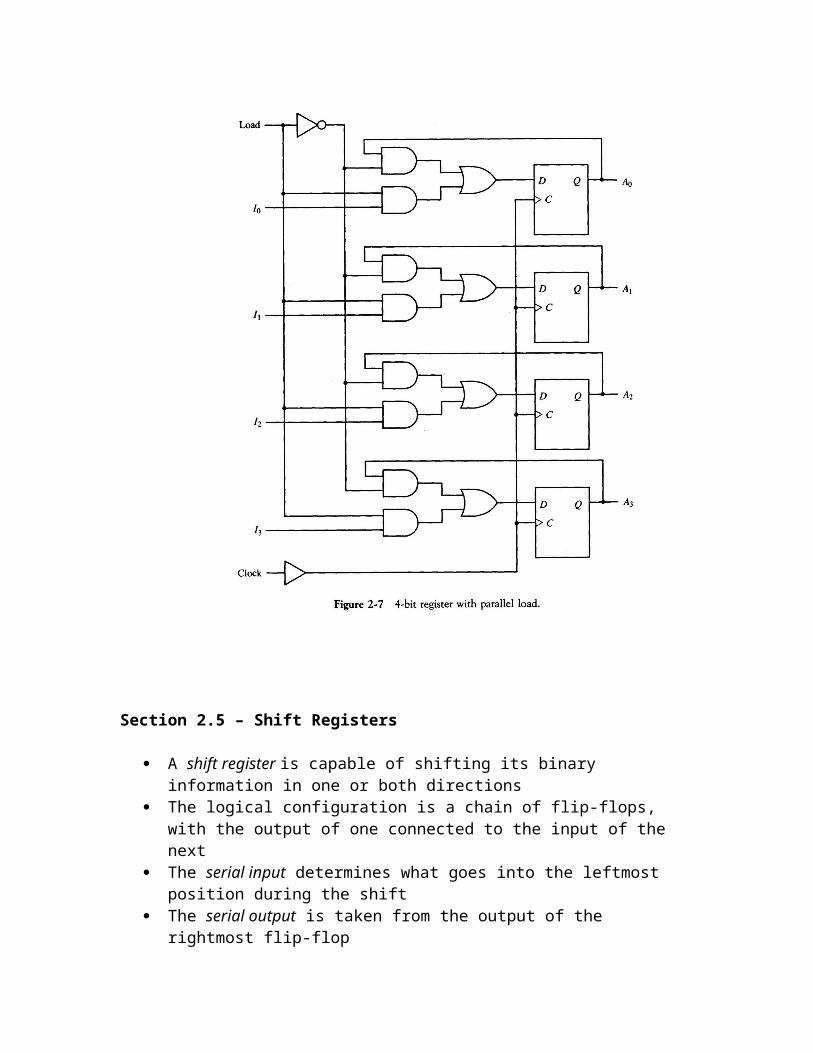
Section 2.4 – Registers
A register is a group of flip-flops with each flip-flop capable of storing one bit of information
An n-bit register has a group of n flip-flops A register may also have combinational gates that perform certain data-processing
tasks The flip-flops hold the data and the gates control when and how new data is
transferred into the register The flip-flops have a common clock input A common clear input is available to reset all the flip-flops asynchronously
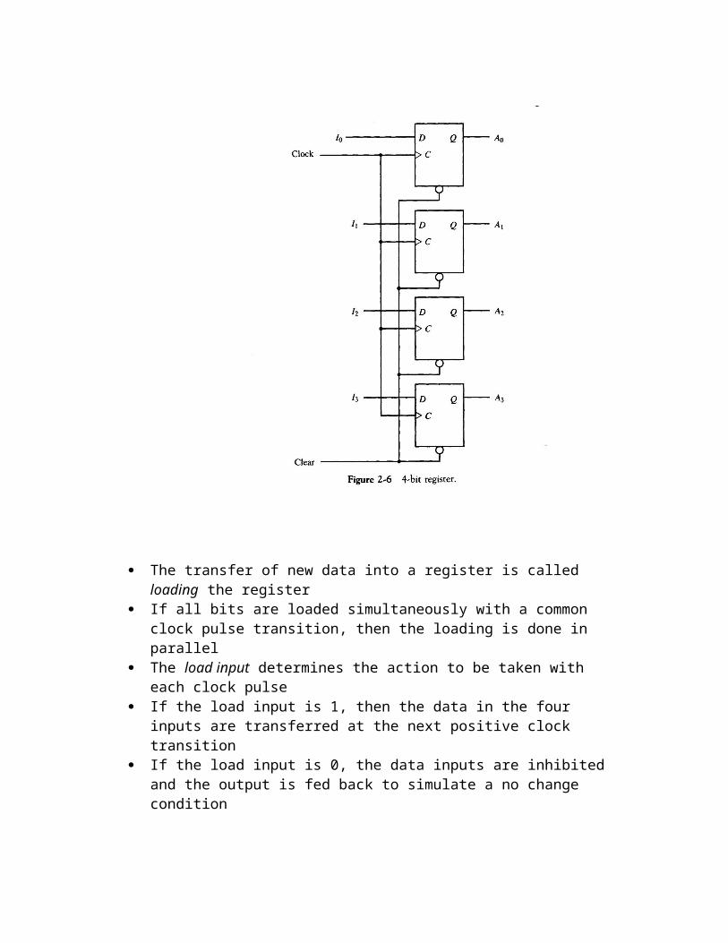
The transfer of new data into a register is called loading the register If all bits are loaded simultaneously with a common clock pulse transition, then
the loading is done in parallel The load input determines the action to be taken with each clock pulse If the load input is 1, then the data in the four inputs are transferred at the next
positive clock transition If the load input is 0, the data inputs are inhibited and the output is fed back to
simulate a no change condition
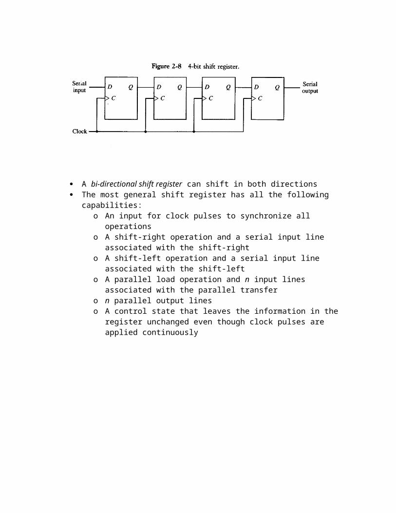
Section 2.5 – Shift Registers
A shift register is capable of shifting its binary information in one or both directions
The logical configuration is a chain of flip-flops, with the output of one connected to the input of the next
The serial input determines what goes into the leftmost position during the shift The serial output is taken from the output of the rightmost flip-flop
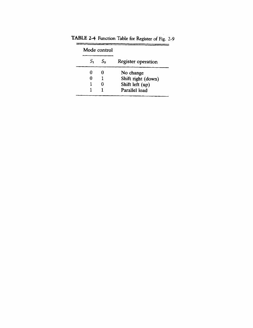
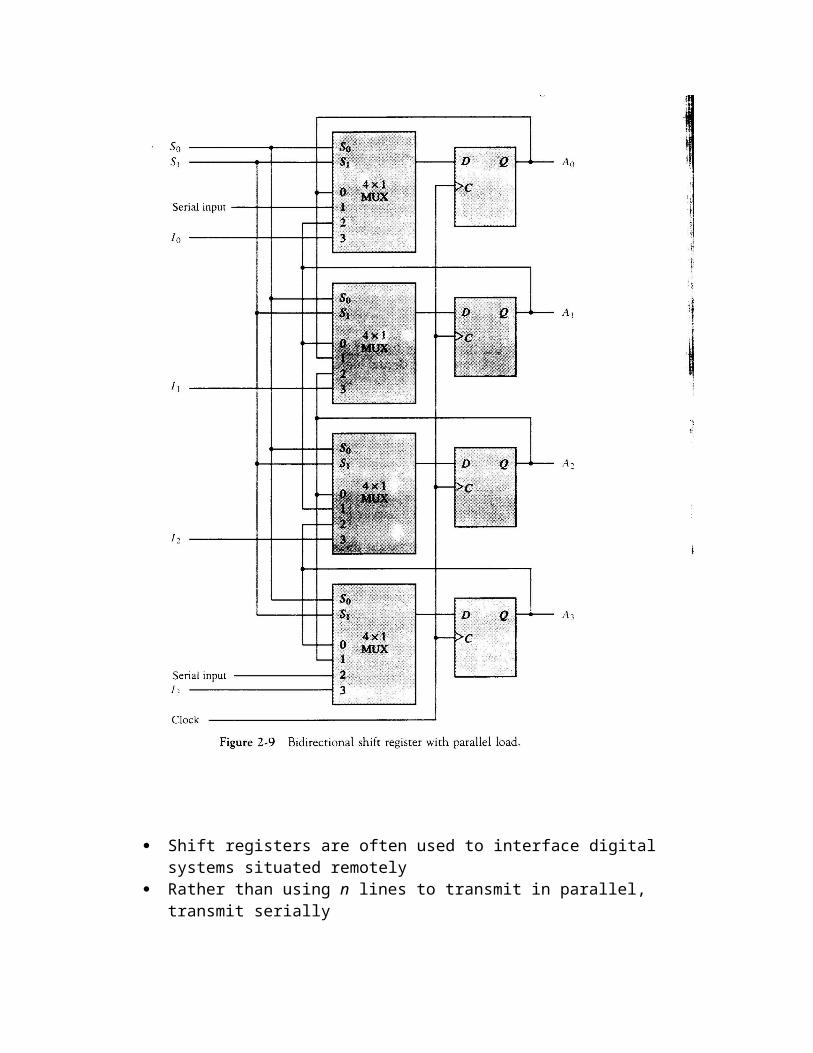
A bi-directional shift register can shift in both directions The most general shift register has all the following capabilities:
o An input for clock pulses to synchronize all operations o A shift-right operation and a serial input line associated with the shift-right o A shift-left operation and a serial input line associated with the shift-left o A parallel load operation and n input lines associated with the parallel
transfer o n parallel output lines o A control state that leaves the information in the register unchanged even
though clock pulses are applied continuously
Shift registers are often used to interface digital systems situated remotely Rather than using n lines to transmit in parallel, transmit serially The receiver converts the incoming serial data to parallel
Section 2.6 – Binary Counters
A register that goes through a predetermined sequence of states upon the application of input pulses is called a counter
The input pulses may be a clock or an external input The input may occur at uniform intervals of time or randomly Used to count the number of occurrences of an event and for generating timing
signals to control the sequence of operations A counter that follows the binary number sequence is a binary counter An n-bit binary counter is a register of n flip-flops and gates that follow a
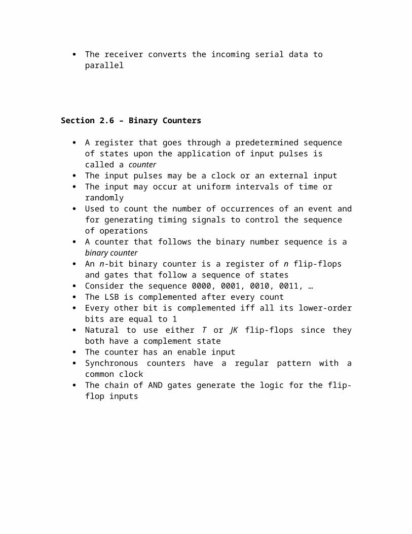
sequence of states Consider the sequence 0000, 0001, 0010, 0011, … The LSB is complemented after every count Every other bit is complemented iff all its lower-order bits are equal to 1 Natural to use either T or JK flip-flops since they both have a complement state The counter has an enable input Synchronous counters have a regular pattern with a common clock The chain of AND gates generate the logic for the flip-flop inputs
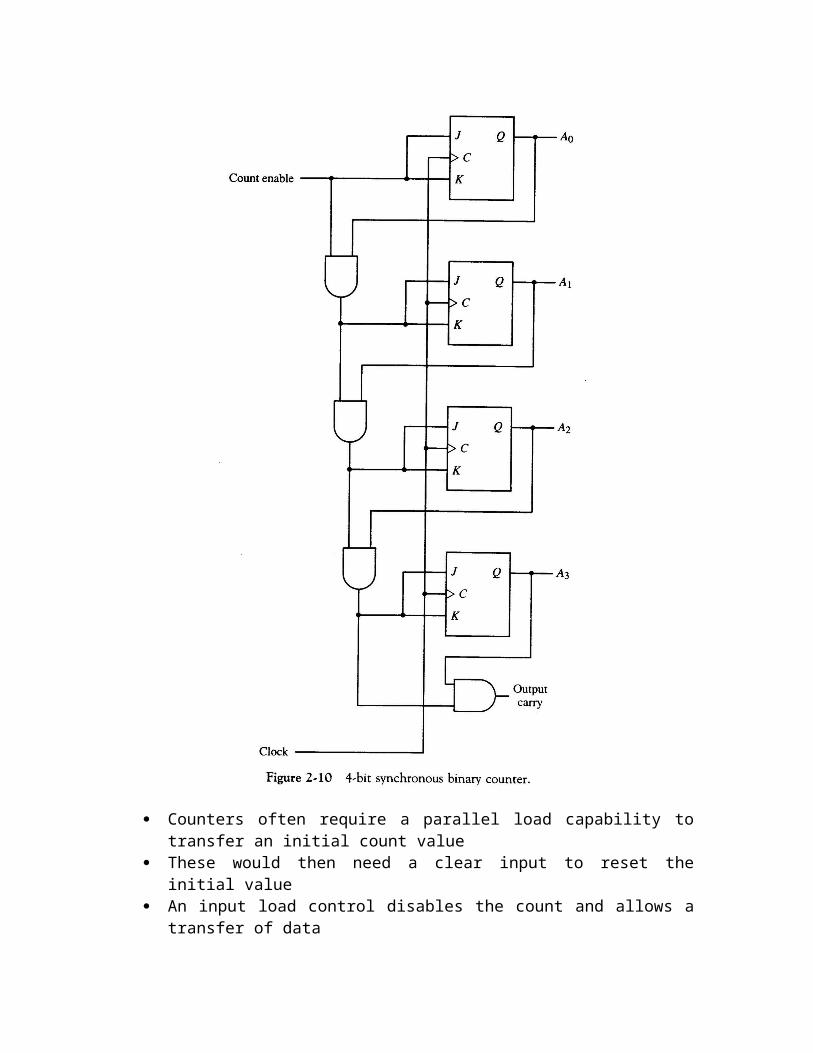
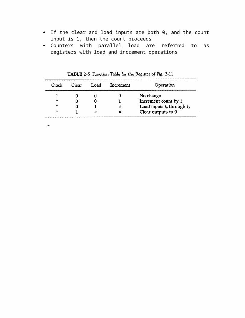
Counters often require a parallel load capability to transfer an initial count value These would then need a clear input to reset the initial value An input load control disables the count and allows a transfer of data If the clear and load inputs are both 0, and the count input is 1, then the count
proceeds Counters with parallel load are referred to as registers with load and increment
operations
Section 2.7 – Memory Unit
A memory unit is a collection of storage cells together with associated circuits to transfer information in and out of storage
The memory stores binary data in groups of bits called words A word can represent an instruction code or alphanumeric characters Each word in memory is assigned an address from 0 to 2k –1, where k is the
number of address lines A decoder inside the memory accepts an address opens the paths needed to select
the bits of the specified word The memory capacity is stated as the total number of bytes that can be stored Refer to the number of bytes using one of the following
o K (kilo) = 210 o M (mega) = 220 o G (giga) = 230
64K = 210, 2M = 221, and 4G = 232 In random-access memory (RAM) the memory cells can be accessed for
information from any desired random location The process of locating a word in memory is the same and requires an equal
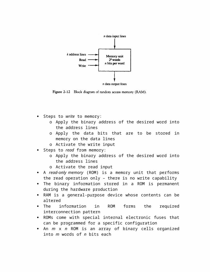
amount of time no matter where the cells are located physically in memory Communication between memory and its environment is achieved via data input
and output lines, address selections lines, and control lines The n data input lines provide the information to be stored in memory The n data output lines supply the information coming out of memory The k address lines provide a binary number of k bits that specify a specific word
or location The two control lines specify the direction of transfer – either read or write
Steps to write to memory:
o Apply the binary address of the desired word into the address lines o Apply the data bits that are to be stored in memory on the data lines o Activate the write input
Steps to read from memory: o Apply the binary address of the desired word into the address lines o Activate the read input
A read-only memory (ROM) is a memory unit that performs the read operation only – there is no write capability
The binary information stored in a ROM is permanent during the hardware production
RAM is a general-purpose device whose contents can be altered The information in ROM forms the required interconnection pattern ROMs come with special internal electronic fuses that can be programmed for a
specific configuration An m x n ROM is an array of binary cells organized into m words of n bits each A ROM has k address lines to select one of m words in memory and n output
lines, one for each bit of the word May have one or more enable inputs for expansion The outputs are a function of only the present input (the address), so it is a
combinational circuit constructed of decoders and OR gates
When used as a memory unit, it stores fixed programs that are not to be altered
and for tables of constants that will not change When used in the design of control units for digital computers, it stores coded
information that represents the sequence of internal control variables to enable the various operations
A control unit that utilizes a ROM is called a microprogrammed control unit The required paths may be programmed in three different ways Mask programming is done by the semiconductor company based upon a truth
table provided by the manufacturer
Programmable read-only memory (PROM) is more economical. PROM units contain all fuses intact and are blown by users
Erasable PROM (EPROM) can be altered using a special ultraviolet light Electrical erasable PROM (EEPROM) can be erased with electrical signals