Embed Size (px)
Citation preview

AMMHU 1
www.ammhu.com A categorized blogging website and an Online Resource Centre For CBSE, RBSE, and Other State Boards — Raj Kumar Parashari, Head Science @ JPHS, Jaipur-302021
SCHOOL NAME SCHOOL NAME SCHOOL
NAME
ADDRESS WITH PINCODE AND PHONE NUMBER
Submitted by Guided by
Student Name [ ]
Class With Section Teacher Name
Class Roll No. Designation
Board Roll No.

AMMHU 2
www.ammhu.com A categorized blogging website and an Online Resource Centre For CBSE, RBSE, and Other State Boards — Raj Kumar Parashari, Head Science @ JPHS, Jaipur-302021
INDEX
1. CERTIFICATE
2. ACKNOWLEDGEMENT
3. AIM
4. APPARATUS REQUIRED
5. PRINCIPLE / THEORY
(a) A Brief Introduction About Semiconductors
(b) A Brief Introduction About LEDs
(c) Principle Used For The Determination Of Plank’s
Constant
6. PROCEDURE
7. OBSERVATIONS With CALCULATIONS
8. RESULT

AMMHU 3
www.ammhu.com A categorized blogging website and an Online Resource Centre For CBSE, RBSE, and Other State Boards — Raj Kumar Parashari, Head Science @ JPHS, Jaipur-302021
CERTIFICATE
This is to certify that _______________________
student of ______ school name _______, class XII Sc
__ has carried out his work for the investigatory
project entitled ______________________-
_________________ under my guidance and
supervision.
Signature of the Teacher
Designation

AMMHU 4
www.ammhu.com A categorized blogging website and an Online Resource Centre For CBSE, RBSE, and Other State Boards — Raj Kumar Parashari, Head Science @ JPHS, Jaipur-302021
ACKNOWLEDGEMENT I __________________________________ a student of
____________________________________,_____________
_ would like to pay my sincere gratitude to my Physics
teacher Mr. __________________________ for helping and
guiding me throughout the completion of the project
report. I would like to thank Mr./Mrs. _______________
_______________________ our school principal/Director
for making school such a wonderful place of learning. I also
would like to thank Mr. ________________ our lab assistant
for the timely assistant in completion of the project.

AMMHU 5
www.ammhu.com A categorized blogging website and an Online Resource Centre For CBSE, RBSE, and Other State Boards — Raj Kumar Parashari, Head Science @ JPHS, Jaipur-302021
AIM
To determine the value of Plank’s constant with the help of
LEDs of different colours
APPARATUS REQUIRED
Red, Blue and green LEDs at least one of each type, a
voltmeter, a rheostat, a battery and an ammeter.
THEORY
(a) Brief Introduction To Semiconductors & PN Diodes
Semiconductors are of two types intrinsic semiconductors and
extrinsic semiconductors
Intrinsic semiconductors are pure pieces of silicon or
germanium without a single foreign particle. It’s electrical
conductivity is totally governed by the thermally excited
electrons and consequently created holes.
In a crystal of germanium, each Ge atom is has four electrons
in its outer orbit so bonded by four neighbouring Ge atoms.
At low temperatures all bonds are intact. As temperature
increases, the thermal energy of the valence electrons
increases. Some of the electron may break free from the
covalent bond and becomes free to conduct. Each of these free
electrons leaves behind vacancy of effective positive charge
called as a hole. Each hole behaves like an apparent free
particle with positive charge. In intrinsic semiconductor, as
each electron creates a hole, so the number density of free
electrons (ne) is equal to number density of holes (nh) i.e. ne =
nh = ni

AMMHU 6
www.ammhu.com A categorized blogging website and an Online Resource Centre For CBSE, RBSE, and Other State Boards — Raj Kumar Parashari, Head Science @ JPHS, Jaipur-302021
Under the application of electric field, holes move in the
direction of the field (due to jumping of bound electrons in
opposite direction from one atom to another) so they act as
positive charge carries and result in a hole current. In
thermally generated free elections give rise to an independent
current, Ie
Total current I = Electron current + Hole current = Ie + Ih
Extrinsic semiconductor are obtained by doping a pure
semiconductor with acceptor or donor impurity atoms. In the
process conductivity is considerably increased. Extrinsic
semiconductors are of 2 types:
N-type semiconductors are Obtained by doping Ge or Si
with pentavalent dopants such as phosphorous P, arsenic As
or antimony Sb.
P-type semiconductors are Obtained by doping Ge or Si with
trivalent or acceptor dopants such as boron B, aluminum Al,
gallium Ga or indium In.
N-Type Semiconductors
The pentavalent impurity atoms substitute the tetravalent Si
(or Ge) atom. It uses 4 of its 5 valance electrons in forming

AMMHU 7
www.ammhu.com A categorized blogging website and an Online Resource Centre For CBSE, RBSE, and Other State Boards — Raj Kumar Parashari, Head Science @ JPHS, Jaipur-302021
four covalent bonds with neighbouring Si atoms, while 5th
electron is loosely bound to the impurity atom. A very small
amount of ionization energy (0.05 eV) for Si or 0.01 eV of
Ge) is required to detach this electron. At room temperature,
thermal energy is enough to set free this electron. The dopant
atom is converted into an ionized + vely charged core. As the
pentavalent impurity donates one extra electron it is called a
donor atom. Such semiconductors have free electrons
contribute by donors and generated by thermal process while
holes are only due to thermal generation.
Hence electrons are majority charge carriers while holes are
minority charge curriers. (ne >> nh) Most current is carried by
negatively charges electrons, so the semiconductor doped with
donor type impurities is called n-type semiconductor.
P-Type Semiconductors
Such a semiconductor is obtained by doping the tetravalent
semiconductor Si (or Ge) with trivalent impurities such as B,
Al, Ga. The impurity uses its three valence electrons in
forming covalent bonds with three neighbouring Si atoms and

AMMHU 8
www.ammhu.com A categorized blogging website and an Online Resource Centre For CBSE, RBSE, and Other State Boards — Raj Kumar Parashari, Head Science @ JPHS, Jaipur-302021
one covalent bond with neighbouring Si is left incomplete due
to deficiency of one electron.
An electron from neighbouring Si-Si covalent bond slides into
this vacant band creating a vacancy or a hole in that bond.
This hole is now available for conduction. The trivalent
impurity atom becomes negatively charged when all its
valence bonds get filled. The trivalent impurity is called an
acceptor atom because it creates a hole which can accept an
electron from the neighbouring bond. These holes are created
due to acceptor atom and thermal generation while electrons
are only due to thermal generation. Hence holes are the
majority change carrier and electrons are minority charge
carrier. Most current is carried by holes and hence these
semiconductors are called p-type semiconductors.
Doping
The process of deliberate addition of a desirable impurity to a
pure semiconductor so as to increase its conductivity is called
doping. The impurity atoms added are called dopants and the
semiconductors doped with impurity are called doped
semiconductors.

AMMHU 9
www.ammhu.com A categorized blogging website and an Online Resource Centre For CBSE, RBSE, and Other State Boards — Raj Kumar Parashari, Head Science @ JPHS, Jaipur-302021
Essential Requirements for a doping process:
1. The semiconductor material should be of very high
purity.
2. The dopant atom should neatly replace semiconductor
atom
3. Size of dopant atom should be almost the same as that of
a semiconductor atom. For this third & fifth group atoms are
must suitable.
4. Dopant should not distort the crystal lattice.
5. Concentration of dopant atoms should be small about 1
ppm ( part per million).
Methods of Doping
1. By adding the impurity atom to any extremely pure
sample of molten semiconductor
2. By heating the crystalline semiconductor in an
atmosphere containing dopant atoms or their molecules so that
the dopant atoms diffuse into the semiconductor.
3. By bombarding the semiconductor with ions of dopant
atoms.
P-N Junctions
It is a single crystal of Ge or Si doped in such a manner that
one portion of it is p-type semiconductor and other part as n-
type semiconductor.
We take thin p-type silicon semiconductor wafer and dope in
to it a small quality of penta-valent impurity. A part of the p-
type semiconductor is converted into n-type. The wafer now
contains p-region and n-region with metallurgical junction

AMMHU 10
www.ammhu.com A categorized blogging website and an Online Resource Centre For CBSE, RBSE, and Other State Boards — Raj Kumar Parashari, Head Science @ JPHS, Jaipur-302021
between two junctions. The device so formed is called as PN
diode.
Formation of depletion region and potential barrier in p-n
junction:
As soon as a p-n junction is formed, majority charge carriers
begin to diffuse from region of higher concentration to region
of lower concentration. Thus the electrons from the n-region
diffuse into the p-region and where they combine with holes
with holes and get neutralized. Similarly, the holes from the p-
region diffuse into n-region where they combine with the
electrons and get neutralized. This is called electron-hole
recombination.
The p region near the junction is left with immobile –ve cores
and n region near the junction is left with +ve cores. The
small region in the vicinity of junction which is depleted of
free charge carriers and has only immobile ions is called
depletion layer. The accumulation of negative charges in the
p-region and positive charges in the n-region sets up potential
difference across the junction. This acts as a barrier and is
called barrier potential VB which opposes the further diffusion
of elections and holes across the junction. The barrier
potential sets up a barrier field in the direction from n-region
to p-region.
The barrier potential VB depends on (i) nature of
semiconductor (ii) temperature (iii) amount of dopants.

AMMHU 11
www.ammhu.com A categorized blogging website and an Online Resource Centre For CBSE, RBSE, and Other State Boards — Raj Kumar Parashari, Head Science @ JPHS, Jaipur-302021
Circuit symbol for p-n junction
The direction of arrow is from P region to n-region. The arrow
indicates the direction in which the conventional current can
flow easily. P side is known as anode and n-side is known as
cathode.
Working of a p-n junction
(a) In case of Forward Biasing
(i) Forward biasing If the positive terminal of a battery is
connected to the P side and the negative terminal of the n side,
then the PN -junction is said to be forward biased.
(i) The effective barrier potential decreases to (VB - V) and
hence energy barrier across the junction decreases.

AMMHU 12
www.ammhu.com A categorized blogging website and an Online Resource Centre For CBSE, RBSE, and Other State Boards — Raj Kumar Parashari, Head Science @ JPHS, Jaipur-302021
(ii) The majority charge carriers from p side and electrons
from n side begin to flow towards the junction.
(iii) The diffusion of electrodes and holes into the depletion
layer decreases its width and
(iv) The effective resistance across the p-n junction
decreases.
When V exceeds VB, the majority charge carriers start flowing
easily across the junction and set up a large current ( mA)
called forward current.
(b) In case of Reverse biasing :
If the positive terminal of a battery is connected to the N-
segment and negative terminal to P-segment, the p-n junction
is said to be reverse biased.
The applied voltage and barrier potential are in same direction
:
(i) Barrier potential increases to VB +V. Hence energy
barrier increase.
(ii) Majority of charge move away from junction, widening
the depletion layer.
(iii) Resistance of p-n junction becomes very large
(iv) no current flows across the junction due to majority
charge carriers.
AMMHU 13
www.ammhu.com A categorized blogging website and an Online Resource Centre For CBSE, RBSE, and Other State Boards — Raj Kumar Parashari, Head Science @ JPHS, Jaipur-302021
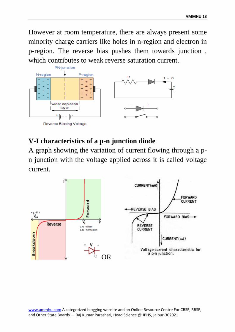
However at room temperature, there are always present some
minority charge carriers like holes in n-region and electron in
p-region. The reverse bias pushes them towards junction ,
which contributes to weak reverse saturation current.
V-I characteristics of a p-n junction diode
A graph showing the variation of current flowing through a p-
n junction with the voltage applied across it is called voltage
current.
OR

AMMHU 14
www.ammhu.com A categorized blogging website and an Online Resource Centre For CBSE, RBSE, and Other State Boards — Raj Kumar Parashari, Head Science @ JPHS, Jaipur-302021
(b) A Brief Introduction About Light Emitting Diode
It is a heavily doped forward biased p-n junction which
spontaneously converts the biasing electrical energy into
optical energy like infrared and visible light.
In a LED, the shorter lead responds to N-or cathode and
longer lead responds to P - or anode side.
A p-n junction made from a translucent semiconductor like
gallium arsenide or indium phosphide is provided with
metalized contact. When it is forward biased through a series
resistance R (to limit the current), light photons are emitted
from non metalized surface of a n region.
When the p-n junction is forward biased, electrons are sent
from N-region to P-region and holes are sent from p region to
n region. Near the junction, the concentration of minority
carriers increases as compared to equilibrium concentration on
either side excess minority carriers combine with majority
carriers. On recombination the energy is released in form of
photons. Photons with energy equal or slightly less than the
band gap are emitted. When the forward bias of the diode is
small, the intensity of emitted light is small. As forward
current increases, intensity of light increases and reaches a
maximum.
1. The colour of light emitted from LED depends on its
bond gap energy.
2. Intensity of light is determined by forward current
through the PN- junction
Choice of Semiconductor material used in LED
The wavelength of visible light ranges from 0.4m to 0.7m.
For semiconductor to emit visible light-min band gap must be

AMMHU 15
www.ammhu.com A categorized blogging website and an Online Resource Centre For CBSE, RBSE, and Other State Boards — Raj Kumar Parashari, Head Science @ JPHS, Jaipur-302021
1.8eV. Compound semiconductor Gallium-Arsenide
phosphide (GaAs1–xPx) is used to make LEDs of different
color.
Advantage of LEDs over conventional incandescent lamps
1. Low operational voltage and less power consumption.
2. Low action and no warm up time required
3. Light emitted is nearly monochromic
4. Long life
5. Fast ON/OFF switching capacity.
Uses of LEDs
1. Infrared LEDs are used in burglar alarm systems
2. Optical communication
3. Image scanning circuits for picture phone
4. Remote controls
Principle Used For The Determination Of Plank’s
Constant:
Given LED is forward biased and applied potential is
increased gradually. Initially current remains zero, for a
particular value of applied potential current breaks (and LED
glows weakly) called as threshold voltage. As applied
potential is further increased current grows rapidly. If V be the
threshold potential, it means that corresponding to it electrons
gains just enough energy overcome barrier potential and
recombine with the hole. Energy released during
recombination is equal or slightly less than the band gap
energy, so h c
E eV

AMMHU 16
www.ammhu.com A categorized blogging website and an Online Resource Centre For CBSE, RBSE, and Other State Boards — Raj Kumar Parashari, Head Science @ JPHS, Jaipur-302021
The Plank constant can be calculated using eV
hc
Procedure :—
(i) Use the forward bias circuit with LED as PN diode.
(ii) Now increase potential across it gradually and record that
value of voltmeter for which LED starts glowing weakly /
ammeter gives some noticeable reading.
Observations With Calculations :—
(a) Least Count of milli-voltmeter = 20 milli-volt
(b) Wavelength of Red LED = 6.33 × 10⁻⁷ m,
Wavelength of Green LED = 5.55 × 10⁻⁷ m,
Wavelength of Blue LED = 4.7 × 10⁻⁷ m,
Reading of the voltmeter for which red LED just starts
glowing
1. 880 milli-volt 2. 860 milli-volt
3. 880 milli-volt 4. 880 milli-volt
Average value of voltmeter reading
V = 875 volt
So, the Plank constant will be
eVh
c
19 7
34
8
1.6 10 0.875 6.33 10h 2.95 10 J s
3 10

AMMHU 17
www.ammhu.com A categorized blogging website and an Online Resource Centre For CBSE, RBSE, and Other State Boards — Raj Kumar Parashari, Head Science @ JPHS, Jaipur-302021
Reading of the voltmeter for which green LED just starts
glowing
1. ------- milli-volt 2. -------- milli-volt
3. -------- milli-volt 4. -------- milli-volt
Average value of voltmeter reading
V = ------ volt
So, the Plank constant will be
eVh
c
h J s
Reading of the voltmeter for which blue LED just starts
glowing
1. ------- milli-volt 2. -------- milli-volt
3. -------- milli-volt 4. -------- milli-volt
Average value of voltmeter reading
V = ------ volt

AMMHU 18
www.ammhu.com A categorized blogging website and an Online Resource Centre For CBSE, RBSE, and Other State Boards — Raj Kumar Parashari, Head Science @ JPHS, Jaipur-302021
So, the Plank constant will be
eVh
c
h J s
Now the average value of Plank’s constant will be
1 1 1h h hh J s
3
Result-
The average value of Plank’s constant is ___________
Bibliography
1. NCERT
2. Google for searching circuits/images and graphs
3.

AMMHU 19
www.ammhu.com A categorized blogging website and an Online Resource Centre For CBSE, RBSE, and Other State Boards — Raj Kumar Parashari, Head Science @ JPHS, Jaipur-302021
Note: — Hand written Investigatory Project
Report should be submitted. Work should be
neat and clean. Avoid unnecessary fancy
decoration of the project report.
Note: — Learn theory, working and related
viva for board practical examination.
Wish you all the best.
Raj Kumar Parashari
Head Science
JPHS, Jaipur


![Becoming A Sustainable School [Your School Name] [Your Name]](https://img.pdfslide.us/doc/110x75/56649dda5503460f94ad0acb/becoming-a-sustainable-school-your-school-name-your-name.jpg)