Embed Size (px)
Citation preview
SCE 0117 - Introdução à Lógica Digital
Introdução aos circuitos lógicos (continuação)
Prof. Vanderlei Bonato

Figure 2.17 Three-variable minterms and maxterms.

Figure 2.18. A three-variable function.

Figure 2.19. Two realizations of a function in Figure 2.18.
f
(a) A minimal sum-of-products realization
f
(b) A minimal product-of-sums realization
x 1
x 2
x 3
x 2
x 1 x 3

• Estudar os exemplos 2.3 e 2.4

Figure 2.20. NAND and NOR gates.
x 1 x 2
x n
x 1 x 2 … x n + + + x 1 x 2
x 1 x 2 +
x 1 x 2
x n
x 1 x 2
x 1 x 2 ⋅ x 1 x 2 … x n ⋅ ⋅ ⋅
(a) NAND gates
(b) NOR gates

x 1 x 2
x 1
x 2
x 1 x 2
x 1 x 2
x 1
x 2
x 1 x 2
x 1 x 2 x 1 x 2 + = (a)
x 1 x 2 + x 1 x 2 = (b)
Figure 2.21. DeMorgan’s theorem in terms of logic gates.

Figure 2.22. Using NAND gates to implement a sum-of-products.
x 1 x 2 x 3 x 4 x 5
x 1 x 2 x 3 x 4 x 5
x 1 x 2 x 3 x 4 x 5

Figure 2.23. Using NOR gates to implement a product-of sums.
x 1 x 2 x 3 x 4 x 5
x 1 x 2 x 3 x 4 x 5
x 1 x 2 x 3 x 4 x 5

• Estudar os exemplos 2.6 e 2.7
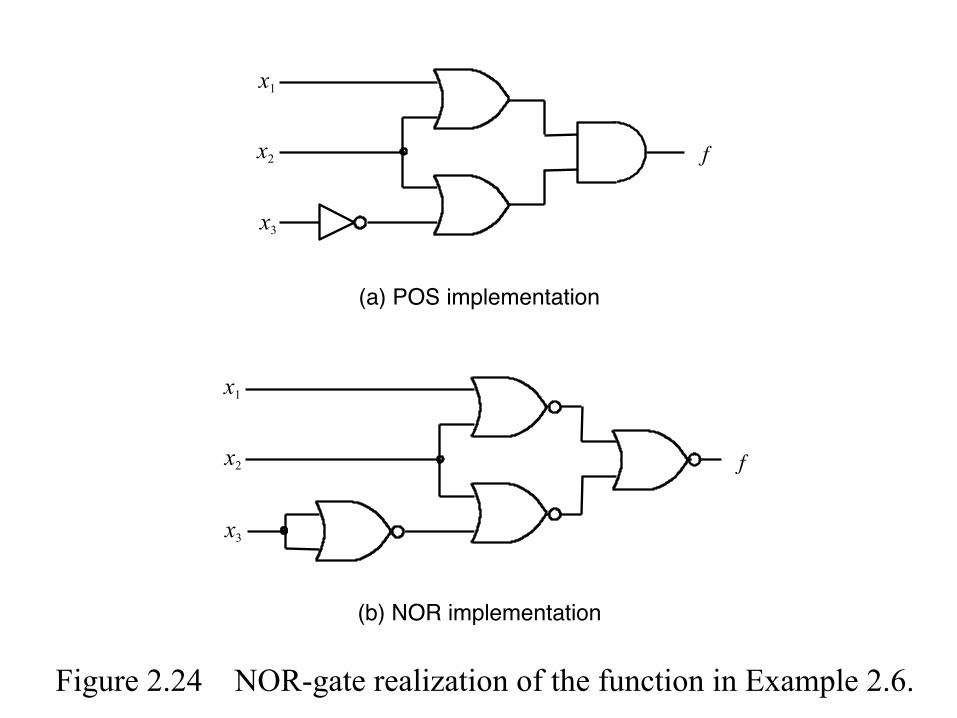
Figure 2.24 NOR-gate realization of the function in Example 2.6.
x1
f
(a) POS implementation
(b) NOR implementation
f
x3
x2
x1
x3
x2

Figure 2.25. NAND-gate realization of the function in Example 2.7.
f
f
(a) SOP implementation
(b) NAND implementation
x1
x3
x2
x3
x2
x1

Figure 2.26. Truth table for a three-way light control.

Figure 2.27. Implementation of the function in Figure 2.26.
f
(a) Sum-of-products realization
(b) Product-of-sums realization
f
x1 x3 x2
x3 x1 x2

0 0 0 0 0 0 1 0 0 1 0 1 0 1 1 1 1 0 0 0 1 0 1 1 1 1 0 0 1 1 1 1
(a) Truth table
s x1 x2 f (s, x1, x2)
f
x 1
x 2 s
f
s
x 1 x 2
0 1
(c) Graphical symbol (b) Circuit
0 1
(d) More compact truth-table representation
f (s, x1, x2) s x1 x2
Figure 2.28. Implementation of a multiplexer.

Figure 2.29. A typical CAD system.
Design conception
VHDL Schematic capture DESIGN ENTRY
Design correct?
Functional simulation No
Yes
No
Synthesis
Physical design
Chip configuration
Timing requirements met?
Timing simulation

Figure 2.30. A simple logic function.
f
x 3
x 1 x 2

Figure 2.31. VHDL entity declaration for the circuit in Figure 2.30.
ENTITY example1 IS
PORT ( x1, x2, x3 : IN BIT ; f : OUT BIT ) ;
END example1 ;

Figure 2.32. VHDL architecture for the entity in Figure 2.31.
ARCHITECTURE LogicFunc OF example1 IS BEGIN
f <= (x1 AND x2) OR (NOT x2 AND x3) ; END LogicFunc ;

Figure 2.33. Complete VHDL code for the circuit in Figure 2.30.

Figure 2.34. VHDL code for a four-input function.

f
g
x 3 x 1
x 2
x 4
Figure 2.35. Logic circuit for the code in Figure 2.34.

Figure 2.36. The Venn diagrams for Example 2.11.
(a) Function A (b) Function B
(c) Function C (d) Function f
x1
x3
x2 x1 x2
x1 x2 x1 x2
x3 x3
x3

x 1 x 2
x 3
x 4
(a)
x 1 x 2
x 3
x 4
(b)
Figure P2.1. Two attempts to draw a four-variable Venn diagram.

x 3
x 2 x 1
x 4
x 3
x 2 x 1
m 0
m 1 m 2
Figure P2.2. A four-variable Venn diagram.

Figure P2.3. A timing diagram representing a logic function.
1 0 1 0 1 0 1 0
x 1
x 2
Time
x 3
f

1 0 1 0 1 0 1 0
x 1
x 2
Time
x 3
f
Figure P2.4. A timing diagram representing a logic function.