Embed Size (px)
Citation preview
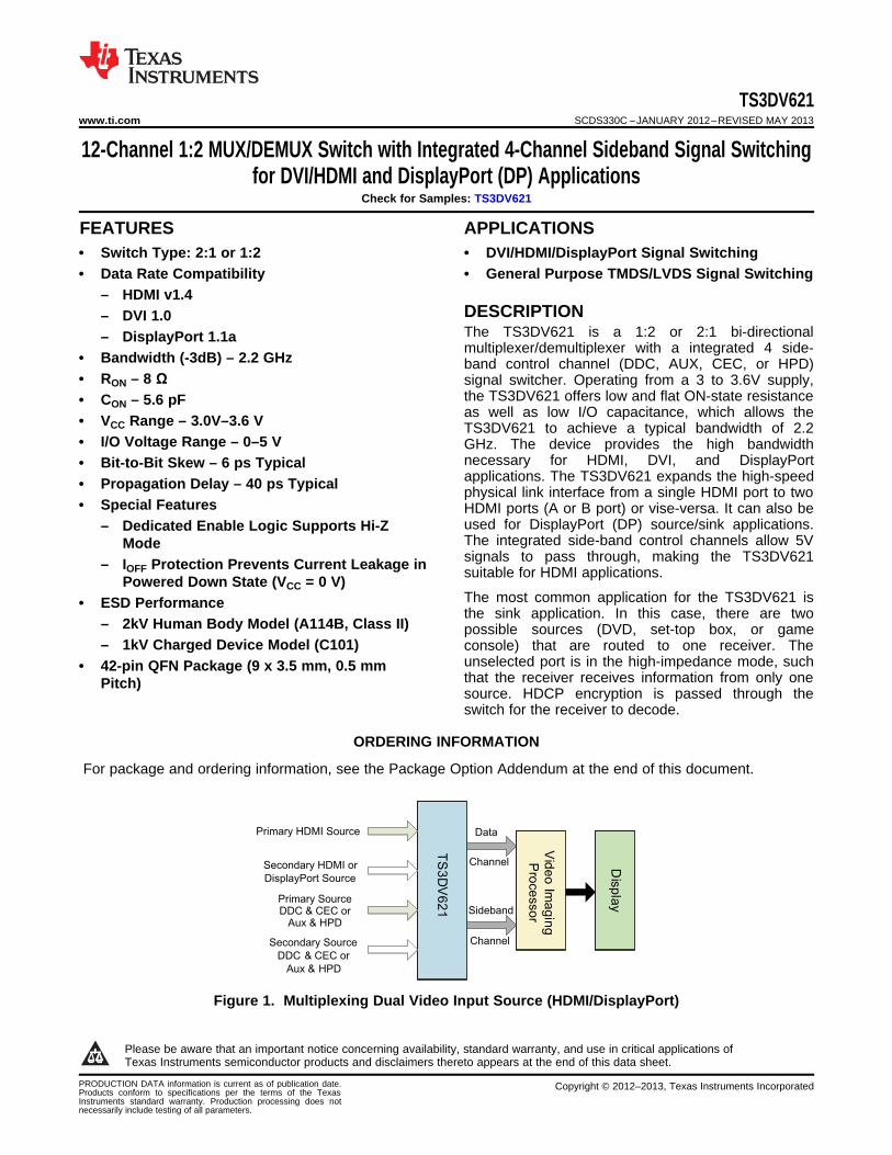
Primary HDMI Source
Primary SourceDDC & CEC or
Aux & HPD
TS
3D
V6
21
Data
Channel
Channel
HD
MI
Re
ce
ive
r
Gra
ph
ic
Pro
cesso
r
Secondary Source
DDC & CEC or
Aux & HPD
Secondary HDMI or
DisplayPort Source
TS
3D
V6
21 Sideband
Vid
eo
Ima
gin
g
Pro
ce
sso
r
Dis
pla
y
TS3DV621www.ti.com SCDS330C –JANUARY 2012–REVISED MAY 2013
12-Channel 1:2 MUX/DEMUX Switch with Integrated 4-Channel Sideband Signal Switchingfor DVI/HDMI and DisplayPort (DP) Applications
Check for Samples: TS3DV621
1FEATURES APPLICATIONS• Switch Type: 2:1 or 1:2 • DVI/HDMI/DisplayPort Signal Switching• Data Rate Compatibility • General Purpose TMDS/LVDS Signal Switching
– HDMI v1.4 spacerDESCRIPTION– DVI 1.0The TS3DV621 is a 1:2 or 2:1 bi-directional– DisplayPort 1.1amultiplexer/demultiplexer with a integrated 4 side-
• Bandwidth (-3dB) – 2.2 GHz band control channel (DDC, AUX, CEC, or HPD)• RON – 8 Ω signal switcher. Operating from a 3 to 3.6V supply,
the TS3DV621 offers low and flat ON-state resistance• CON – 5.6 pFas well as low I/O capacitance, which allows the
• VCC Range – 3.0V–3.6 V TS3DV621 to achieve a typical bandwidth of 2.2• I/O Voltage Range – 0–5 V GHz. The device provides the high bandwidth
necessary for HDMI, DVI, and DisplayPort• Bit-to-Bit Skew – 6 ps Typicalapplications. The TS3DV621 expands the high-speed• Propagation Delay – 40 ps Typicalphysical link interface from a single HDMI port to two
• Special Features HDMI ports (A or B port) or vise-versa. It can also beused for DisplayPort (DP) source/sink applications.– Dedicated Enable Logic Supports Hi-ZThe integrated side-band control channels allow 5VModesignals to pass through, making the TS3DV621– IOFF Protection Prevents Current Leakage in suitable for HDMI applications.
Powered Down State (VCC = 0 V)The most common application for the TS3DV621 is• ESD Performancethe sink application. In this case, there are two
– 2kV Human Body Model (A114B, Class II) possible sources (DVD, set-top box, or game– 1kV Charged Device Model (C101) console) that are routed to one receiver. The
unselected port is in the high-impedance mode, such• 42-pin QFN Package (9 x 3.5 mm, 0.5 mmthat the receiver receives information from only onePitch)source. HDCP encryption is passed through theswitch for the receiver to decode.
ORDERING INFORMATION
For package and ordering information, see the Package Option Addendum at the end of this document.
Figure 1. Multiplexing Dual Video Input Source (HDMI/DisplayPort)
1
Please be aware that an important notice concerning availability, standard warranty, and use in critical applications ofTexas Instruments semiconductor products and disclaimers thereto appears at the end of this data sheet.
PRODUCTION DATA information is current as of publication date. Copyright © 2012–2013, Texas Instruments IncorporatedProducts conform to specifications per the terms of the TexasInstruments standard warranty. Production processing does notnecessarily include testing of all parameters.

37
35
33
38
36
34
31
29
30
32
2
4
6
8
12
10
14
16
1
3
5
7
11
9
13
15
18
20
19
17 22
24
21
42
40
41
39
23
26
28
27
25
D1+A
D3+A
D1–A
D3–A
D2+A
AUX+A
D2–A
AUX–A
D1+B
D3+B
D1–B
D3–B
D2+B
AUX+B
D2–B
AUX–B
VCC
VCC
D0+
D0–
D1+
EN
AUX–
D1–
D2+
D2–
SEL1
SEL2
D3+
D3–
AUX+
HPD
CEC
VCC
HP
DA
CE
CB
CE
CA
HP
DB
D0
–B
D0+
B
D0+
A
D0
–A
GND
TS3DV621SCDS330C –JANUARY 2012–REVISED MAY 2013 www.ti.com
This integrated circuit can be damaged by ESD. Texas Instruments recommends that all integrated circuits be handled withappropriate precautions. Failure to observe proper handling and installation procedures can cause damage.
ESD damage can range from subtle performance degradation to complete device failure. Precision integrated circuits may be moresusceptible to damage because very small parametric changes could cause the device not to meet its published specifications.
PIN FUNCTIONSPIN
I/O TYPE DESCRIPTIONNAME NO.
VCC 1,17, 30 Power Supply Voltage
GND PowerPad Ground Ground
EN 8 I Enable Input
SEL1 9 I Select Input 1
SEL2 10 I Select Input 2
D0+A 41 I/O Port A, Lane 0, +ve signal
D0-A 39 I/O Port A, Lane 0, -ve signal
D1+A 38 I/O Port A, Lane 1, +ve signal
D1-A 36 I/O Port A, Lane 1, -ve signal
D2+A 34 I/O Port A, Lane 2, +ve signal
D2-A 32 I/O Port A, Lane 2, -ve signal
D3+A 29 I/O Port A, Lane 3, +ve signal
D3-A 27 I/O Port A, Lane 3, -ve signal
D0+B 42 I/O Port B, Lane 0, +ve signal
D0-B 40 I/O Port B, Lane 0, -ve signal
D1+B 37 I/O Port B, Lane 1, +ve signal
D1-B 35 I/O Port B, Lane 1, -ve signal
D2+B 33 I/O Port B, Lane 2, +ve signal
D2-B 31 I/O Port B, Lane 2, -ve signal
D3+B 28 I/O Port B, Lane 3, +ve signal
D3-B 26 I/O Port B, Lane 3, -ve signal
D0+ 2 I/O Common Port, Lane 0, +ve signal
D0– 3 I/O Common Port, Lane 0, -ve signal
D1+ 4 I/O Common Port, Lane 1, +ve signal
D1– 5 I/O Common Port, Lane 1, -ve signal
D2+ 6 I/O Common Port, Lane 2, +ve signal
D2– 7 I/O Common Port, Lane 2, -ve signal
D3+ 11 I/O Common Port, Lane 3, +ve signal
D3- 12 I/O Common Port, Lane 3, -ve signal
AUX+A 25 I/O +ve AUX Channel for Port A
AUX-A 23 I/O -ve AUX Channel for Port A
HPDA 21 I/O Port A HPD
CECA 19 I/O Port A CEC
AUX+B 24 I/O +ve AUX Channel for Port B
AUX-B 22 I/O -ve AUX Channel for Port B
HPDB 20 I/O Port B HPD
CECB 18 I/O Port B CEC
AUX+ 13 I/O +ve AUX Channel for Common Port
AUX– 14 I/O -ve AUX Channel for Common Port
HPD 15 I/O HPD for Common Port
CEC 16 I/O CEC for Common Port
2 Submit Documentation Feedback Copyright © 2012–2013, Texas Instruments Incorporated
Product Folder Links :TS3DV621

D0+
SEL1 Control Logic
SEL2
AUX+
AUX–
HPD
CEC
EN
AUX+A
AUX–A
HPDA
CECA
AUX+B
AUX–B
HPDB
CECB
D0–
D1+
D1–
D2+
D2–
D3+
D3–
D0+A
D0–A
D1+A
D1–A
D2+A
D2–A
D3+A
D3–A
D0+B
D0–B
D1+B
D1–B
D2+B
D2–B
D3+B
D3–B
TS3DV621www.ti.com SCDS330C –JANUARY 2012–REVISED MAY 2013
LOGIC DIAGRAM
Table 1. FUNCTION TABLE
EN SEL1 SEL2 FUNCTION
L X X All I/O = High Impedance
Output port A = InputH L (1) L (1)
Output Port B = High Impedance
Output Port A = High ImpedanceH H (1) H (1)
Output Port B = Input
(1) Tie SEL1 and SEL2 together for easy output control
Copyright © 2012–2013, Texas Instruments Incorporated Submit Documentation Feedback 3
Product Folder Links :TS3DV621
D0+
D0-
D2+
D1-D1+
D3+
D2-
D3-
Cab_DetectAUX/DDC
HPD
AUX/DDC
TS3DV621
DP/HDMI
Switch
Dual Mode
DisplayPort
Source
Dual Mode
DisplayPort
Connector
HDMI
Connector
D0+
D0-
D2+
D1-D1+
D3+
D2-
D3-
Cab_DetectAUX-
HPD
AUX+
D0+
D0-
D2+
D1-D1+
D3+
D2-
D3-
DDC_DATA
HPD
DDC_CLK
D0+
D0-
D2+
D1-D1+
D3+
D2-
D3-
CECDDC DATA
HPD
DDC CLK
TS3DV621
HDMI Switch
HDMI
Transmitter 1
HDMI
Receiver
Display
(DLP, LCD, TV,
PDP, HDTV)
HDMI Scalar/
Video Decoder
D0+A
D0-A
D2+A
D1-AD1+A
D3+A
D2-A
D3-A
CEC_ADDC DATA _A
HPD_A
DDC CLK _A
HDMI
Transmitter 1
D0+B
D0-B
D2+B
D1-B
D1+B
D3+B
D2-B
D3-B
CEC_BDDC DATA _B
HPD_B
DDC CLK _B
TS3DV621SCDS330C –JANUARY 2012–REVISED MAY 2013 www.ti.com
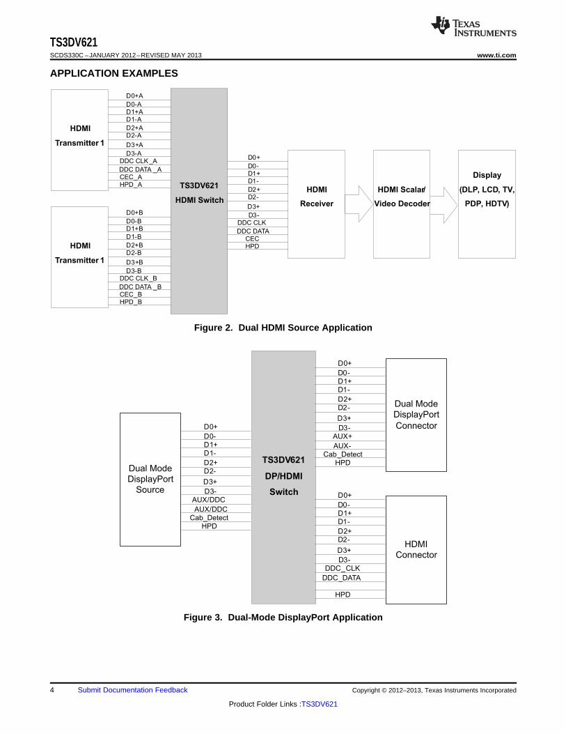
APPLICATION EXAMPLES
Figure 2. Dual HDMI Source Application
Figure 3. Dual-Mode DisplayPort Application
4 Submit Documentation Feedback Copyright © 2012–2013, Texas Instruments Incorporated
Product Folder Links :TS3DV621

TS3DV621www.ti.com SCDS330C –JANUARY 2012–REVISED MAY 2013
ABSOLUTE MAXIMUM RATINGS (1)
over operating free-air temperature range (unless otherwise noted)
MIN MAX UNIT
VCC Supply voltage range -0.5 4.6 V
VI/O Analog voltage range (2) (3) (4) All I/O –0.5 7 V
VIN Digital input voltage range (2) (3) SEL1, SEL2 –0.5 7 V
II/OK Analog port diode current VI/O < 0 –50 mA
IIK Digital input clamp current VIN < 0 –50 mA
II/O On-state switch current (5) All I/O –128 128 mA
IDD Continuous current through VDD or GND –100 100 mAIGND
θJA Package thermal impedance (6) RUA package 31.8 °C/W
Tstg Storage temperature range –65 150 °C
(1) Stresses beyond those listed under "Absolute Maximum Ratings" may cause permanent damage to the device. These are stress ratingsonly and functional operation of the device at these or any other conditions beyond those indicated under “recommended operatingconditions” is not implied. Exposure to absolute-maximum-rated conditions for extended periods may affect device reliability.
(2) All voltages are with respect to ground, unless otherwise specified.(3) The input and output voltage ratings may be exceeded if the input and output clamp-current ratings are observed.(4) VI and VO are used to denote specific conditions for VI/O.(5) II and IO are used to denote specific conditions for II/O.(6) The package thermal impedance is calculated in accordance with JESD 51-7
RECOMMENDED OPERATING CONDITIONS (1)
MIN MAX UNIT
VCC Supply voltage 3 3.6 V
VIH High-level control input voltage SEL1, SEL2 2 5.5 V
VIL Low-level control input voltage SEL1, SEL2 0 0.8 V
VIN Input voltage SEL1, SEL2 0 5.5 V
VI/O Input/Output voltage 0 5.5 V
TA Operating free-air temperature –40 85 °C
(1) All unused control inputs of the device must be held at VDD or GND to ensure proper device operation. Refer to the TI applicationreport, Implications of Slow or Floating CMOS Inputs, literature number SCBA004.
Copyright © 2012–2013, Texas Instruments Incorporated Submit Documentation Feedback 5
Product Folder Links :TS3DV621
TS3DV621SCDS330C –JANUARY 2012–REVISED MAY 2013 www.ti.com
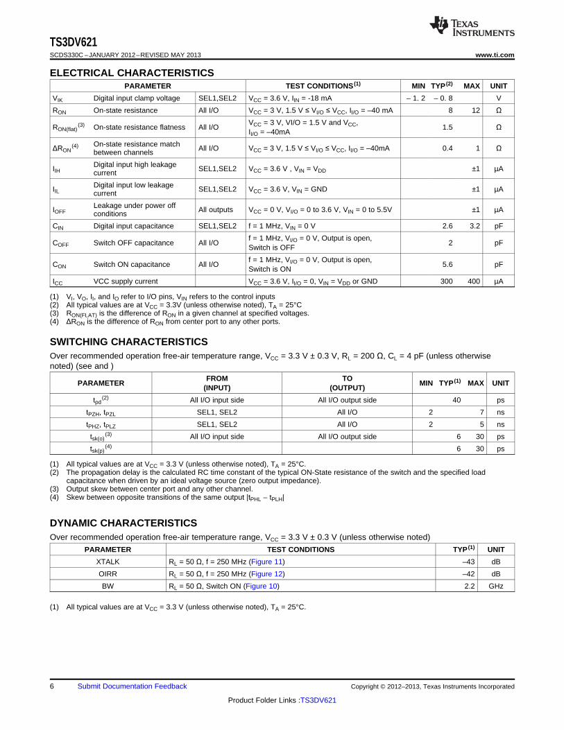
ELECTRICAL CHARACTERISTICSPARAMETER TEST CONDITIONS (1) MIN TYP (2) MAX UNIT
VIK Digital input clamp voltage SEL1,SEL2 VCC = 3.6 V, IIN = -18 mA – 1. 2 – 0. 8 V
RON On-state resistance All I/O VCC = 3 V, 1.5 V ≤ VI/O ≤ VCC, II/O = –40 mA 8 12 ΩVCC = 3 V, VI/O = 1.5 V and VCC,
RON(flat)(3) On-state resistance flatness All I/O 1.5 Ω
II/O = –40mA
On-state resistance matchΔRON(4) All I/O VCC = 3 V, 1.5 V ≤ VI/O ≤ VCC, II/O = –40mA 0.4 1 Ωbetween channels
Digital input high leakageIIH SEL1,SEL2 VCC = 3.6 V , VIN = VDD ±1 µAcurrent
Digital input low leakageIIL SEL1,SEL2 VCC = 3.6 V, VIN = GND ±1 µAcurrent
Leakage under power offIOFF All outputs VCC = 0 V, VI/O = 0 to 3.6 V, VIN = 0 to 5.5V ±1 µAconditions
CIN Digital input capacitance SEL1,SEL2 f = 1 MHz, VIN = 0 V 2.6 3.2 pF
f = 1 MHz, VI/O = 0 V, Output is open,COFF Switch OFF capacitance All I/O 2 pF
Switch is OFF
f = 1 MHz, VI/O = 0 V, Output is open,CON Switch ON capacitance All I/O 5.6 pF
Switch is ON
ICC VCC supply current VCC = 3.6 V, II/O = 0, VIN = VDD or GND 300 400 µA
(1) VI, VO, II, and IO refer to I/O pins, VIN refers to the control inputs(2) All typical values are at VCC = 3.3V (unless otherwise noted), TA = 25°C(3) RON(FLAT) is the difference of RON in a given channel at specified voltages.(4) ΔRON is the difference of RON from center port to any other ports.
SWITCHING CHARACTERISTICSOver recommended operation free-air temperature range, VCC = 3.3 V ± 0.3 V, RL = 200 Ω, CL = 4 pF (unless otherwisenoted) (see and )
FROM TOPARAMETER MIN TYP (1) MAX UNIT
(INPUT) (OUTPUT)
tpd(2) All I/O input side All I/O output side 40 ps
tPZH, tPZL SEL1, SEL2 All I/O 2 7 ns
tPHZ, tPLZ SEL1, SEL2 All I/O 2 5 ns
tsk(o)(3) All I/O input side All I/O output side 6 30 ps
tsk(p)(4) 6 30 ps
(1) All typical values are at VCC = 3.3 V (unless otherwise noted), TA = 25°C.(2) The propagation delay is the calculated RC time constant of the typical ON-State resistance of the switch and the specified load
capacitance when driven by an ideal voltage source (zero output impedance).(3) Output skew between center port and any other channel.(4) Skew between opposite transitions of the same output |tPHL – tPLH|
DYNAMIC CHARACTERISTICSOver recommended operation free-air temperature range, VCC = 3.3 V ± 0.3 V (unless otherwise noted)
PARAMETER TEST CONDITIONS TYP (1) UNIT
XTALK RL = 50 Ω, f = 250 MHz (Figure 11) –43 dB
OIRR RL = 50 Ω, f = 250 MHz (Figure 12) –42 dB
BW RL = 50 Ω, Switch ON (Figure 10) 2.2 GHz
(1) All typical values are at VCC = 3.3 V (unless otherwise noted), TA = 25°C.
6 Submit Documentation Feedback Copyright © 2012–2013, Texas Instruments Incorporated
Product Folder Links :TS3DV621

-140
-120
-100
-80
-60
-40
-20
0
1.00E+05 1.00E+06 1.00E+07 1.00E+08 1.00E+09 1.00E+10
f - Frequency - Hz
Att
en
uati
on
- d
B
R-
ON
W
V - Input Voltage - VI
1.4 1.9 2.4 2.9 3.47.4
7.6
7.8
8.0
8.2
8.4
8.6
8.8
9.0
-12
-10
-8
-6
-4
-2
0
1.00E+05 1.00E+06 1.00E+07 1.00E+08 1.00E+09 1.00E+10
f - Frequency - Hz
Att
en
uati
on
- d
B
-140
-120
-100
-80
-60
-40
-20
0
1.00E+05 1.00E+06 1.00E+07 1.00E+08 1.00E+09 1.00E+10
f - Frequency - HzA
tten
uati
on
- d
B
TS3DV621www.ti.com SCDS330C –JANUARY 2012–REVISED MAY 2013
OPERATING CHARACTERISTICS
Figure 4. Gain vs Frequency Figure 5. Off Isolation vs Frequency
Figure 6. Crosstalk vs Frequency Figure 7. RON vs VIN
Copyright © 2012–2013, Texas Instruments Incorporated Submit Documentation Feedback 7
Product Folder Links :TS3DV621
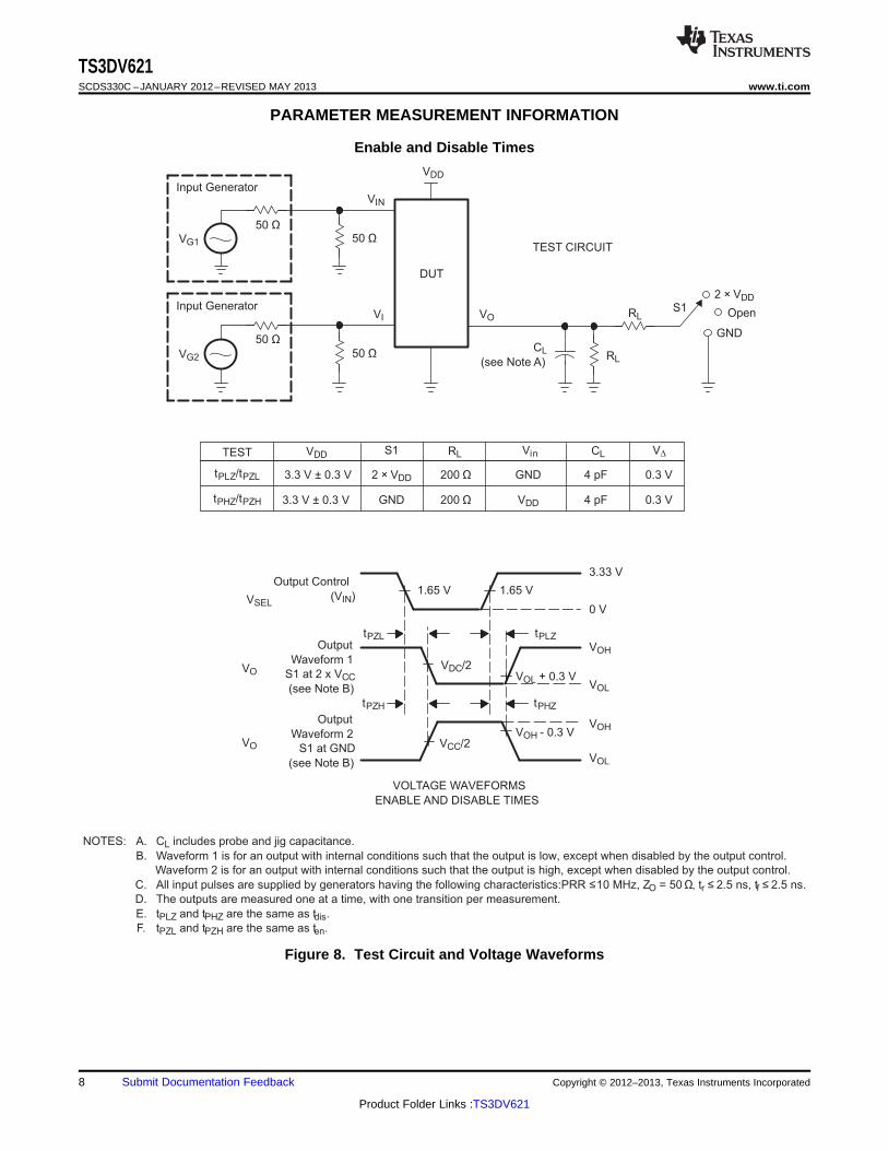
CL
(see Note A)
TEST CIRCUIT
S12 × VDD
Open
GND
RL
RL
NOTES: A. CL includes probe and jig capacitance.
B. Waveform 1 is for an output with internal conditions such that the output is low, except when disabled by the output control.
Waveform 2 is for an output with internal conditions such that the output is high, except when disabled by the output control.
C. All input pulses are supplied by generators having the following characteristics:PRR ≤10 MHz, ZO = 50 Ω, tr ≤ 2.5 ns, tf ≤ 2.5 ns.
D. The outputs are measured one at a time, with one transition per measurement.
E. tPLZ and tPHZ are the same as tdis.
F. tPZL and tPZH are the same as ten.
50 Ω
VG1
VDD
DUT
50 Ω
VIN
50 Ω
VG2 50 Ω
VI
TEST RLS1 V∆CLVDD Vin
tPLZ/tPZL 2 × VDD 200 Ω GND 4 pF 0.3 V
Input Generator
Input GeneratorVO
tPHZ/tPZH GND 200 Ω VDD 4 pF 0.3 V
tPZL
VOH - 0.3 V
VOLTAGE WAVEFORMS
ENABLE AND DISABLE TIMES
VCC/2
VDC/2
Output Control
(VIN)
VOH
VOL + 0.3 V
VOH
VOL
0 V
tPZH
tPLZ
tPHZ
Output
Waveform 2
S1 at GND
(see Note B)
Output
Waveform 1
S1 at 2 x VCC
(see Note B)
VOL
VO
VSEL
VO
3.3 V ± 0.3 V
3.3 V ± 0.3 V
1.65 V1.65 V
3.33 V
TS3DV621SCDS330C –JANUARY 2012–REVISED MAY 2013 www.ti.com
PARAMETER MEASUREMENT INFORMATION
Enable and Disable Times
Figure 8. Test Circuit and Voltage Waveforms
8 Submit Documentation Feedback Copyright © 2012–2013, Texas Instruments Incorporated
Product Folder Links :TS3DV621

CL
(see Note A)
TEST CIRCUIT
S12 × VDD
Open
GND
RL
RL
VOH
VOL
VOLTAGE WAVEFORMS
OUTPUT SKEW (tsk(o))
Data Out at
YB1 or YB 2
NOTES: A. CL includes probe and jig capacitance.
B. Waveform 1 is for an output with internal conditions such that the output is low, except when disabled by the output control.
Waveform 2 is for an output with internal conditions such that the output is high, except when disabled by the output control.
C. All input pulses are supplied by generators having the following characteristics: PRR ≤10 MHz, ZO = 50 Ω, tr ≤ 2.5 ns, tf ≤ 2.5 ns.
D. The outputs are measured one at a time, with one transition per measurement.
50 Ω
VG1
VDD
DUT
50 Ω
VSEL
50 Ω
VG2 50 Ω
VI
Input Generator
Input GeneratorVO
(VOH + VOL)/2
VOH
VOL
Data Out at
XB1 or XB 2(VOH + VOL)/2
3.5 V
1.5 V
Data In at
Ax or Ay
tPLHx tPHLx
tsk(o) tsk(o)
tPLHy tPHLy
tsk(o) = tPLHy − tPLHx or tPHLy − tPHLx
VOH
VOL
VOLTAGE WAVEFORMS
PULSE SKEW [t sk(p)]
Output (VOH + VOL)/2
Input
tPLH tPHL
tsk(p) = tPHL − tPLH
VO
VI
VO
2.5 V
3.5 V
1.5 V
2.5 V
TEST RLS1 CL
3.3 V ± 0.3 V
VCC Vin
tsk(p)
tsk(o)
3.3 V ± 0.3V
Open
Open
200 Ω VCC or GND
VCC or GND
4 pF
4 pF200 Ω
TS3DV621www.ti.com SCDS330C –JANUARY 2012–REVISED MAY 2013
PARAMETER MEASUREMENT INFORMATION (continued)
Skew
Figure 9. Test Circuit and Voltage Waveforms
Copyright © 2012–2013, Texas Instruments Incorporated Submit Documentation Feedback 9
Product Folder Links :TS3DV621

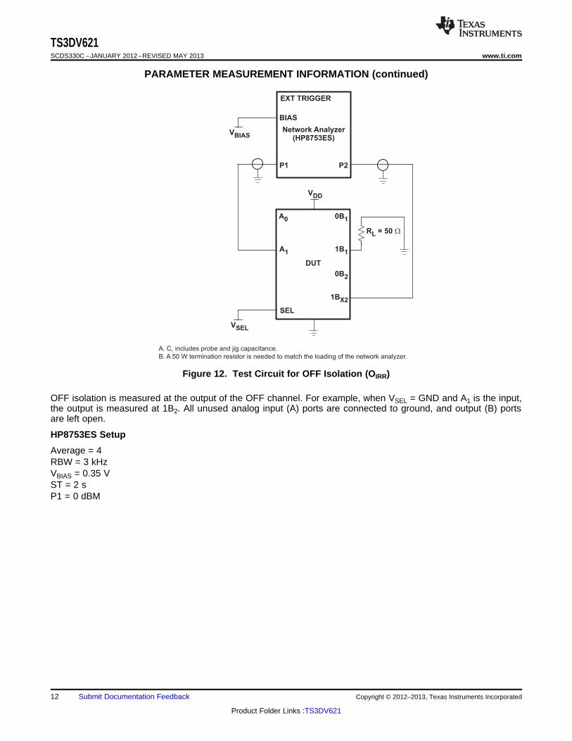
EXT TRIGGER
BIAS
Network Analyzer(HP8753ES)
P1 P2
VCC
AX BX
SELDUT
VBIAS
VSEL
TS3DV621SCDS330C –JANUARY 2012–REVISED MAY 2013 www.ti.com
PARAMETER MEASUREMENT INFORMATION (continued)
Figure 10. Test Circuit for Frequency Response (BW)
Frequency response is measured at the output of the ON channel. For example, when VSEL = 0 and A0 is theinput, the output is measured at B0. All unused analog I/O ports are left open.
HP8753ES Setup
Average = 4RBW = 3 kHzVBIAS = 0.35 VST = 2 sP1 = 0 dBM
10 Submit Documentation Feedback Copyright © 2012–2013, Texas Instruments Incorporated
Product Folder Links :TS3DV621

VSEL
A. C includes probe and jig capacitance.
B. A 50 W termination resistor is needed to match the loading of the network analyzer.L
VBIAS
EXT TRIGGER
BIAS
Network Analyzer(HP8753ES)
P1 P2
A0
A1
A2
A3
SEL
BX
BX
BX
BX
BX
BX
BX
BX
VCC
R = 50L W
R = 50L W
TS3DV621www.ti.com SCDS330C –JANUARY 2012–REVISED MAY 2013
PARAMETER MEASUREMENT INFORMATION (continued)
Figure 11. Test Circuit for Crosstalk (XTALK)
Crosstalk is measured at the output of the nonadjacent ON channel. For example, when VSEL = 0 and A1 is theinput, the output is measured at A3. All unused analog input (A) ports are connected to GND, and output (B)ports are left open.
HP8753ES Setup
Average = 4RBW = 3 kHzVBIAS = 0.35 VST = 2 sP1 = 0 dBM
Copyright © 2012–2013, Texas Instruments Incorporated Submit Documentation Feedback 11
Product Folder Links :TS3DV621
VDD
A0 0B1
SEL
DUT
VBIAS
VSEL
EXT TRIGGER
BIAS
Network Analyzer(HP8753ES)
P1 P2
A1 1B1
0B2
1BX2
R = 50L W
A. C includes probe and jig capacitance.
B. A 50 W termination resistor is needed to match the loading of the network analyzer.L
TS3DV621SCDS330C –JANUARY 2012–REVISED MAY 2013 www.ti.com
PARAMETER MEASUREMENT INFORMATION (continued)
Figure 12. Test Circuit for OFF Isolation (OIRR)
OFF isolation is measured at the output of the OFF channel. For example, when VSEL = GND and A1 is the input,the output is measured at 1B2. All unused analog input (A) ports are connected to ground, and output (B) portsare left open.
HP8753ES Setup
Average = 4RBW = 3 kHzVBIAS = 0.35 VST = 2 sP1 = 0 dBM
12 Submit Documentation Feedback Copyright © 2012–2013, Texas Instruments Incorporated
Product Folder Links :TS3DV621

TS3DV621www.ti.com SCDS330C –JANUARY 2012–REVISED MAY 2013
REVISION HISTORY
Changes from Original (January 2012) to Revision A Page
• Changed CON value in FEATURES from 5.6 pF to 4 pF. ..................................................................................................... 1
• Deleted LEVEL-SHIFTING REQUIREMENT FOR DUAL-MODE DP/HDMI APPLICATION section from document. ......... 4
• Added CON TYP value to the ELECTRICAL CHARACTERISTICS table. ............................................................................. 6
Changes from Revision A (February 2012) to Revision B Page
• Changed CON value from 4 pF to 5.6 pF. ............................................................................................................................. 1
• Changed CON TYP value to the ELECTRICAL CHARACTERISTICS table. ........................................................................ 6
Changes from Revision B (May 2012) to Revision C Page
• Updated APPLICATIONS. .................................................................................................................................................... 1
Copyright © 2012–2013, Texas Instruments Incorporated Submit Documentation Feedback 13
Product Folder Links :TS3DV621

PACKAGE OPTION ADDENDUM
www.ti.com 31-Aug-2016
Addendum-Page 1
PACKAGING INFORMATION
Orderable Device Status(1)
Package Type PackageDrawing
Pins PackageQty
Eco Plan(2)
Lead/Ball Finish(6)
MSL Peak Temp(3)
Op Temp (°C) Device Marking(4/5)
Samples
TS3DV621RUAR ACTIVE WQFN RUA 42 3000 Green (RoHS& no Sb/Br)
CU NIPDAU Level-1-260C-UNLIM -40 to 85 SD621
(1) The marketing status values are defined as follows:ACTIVE: Product device recommended for new designs.LIFEBUY: TI has announced that the device will be discontinued, and a lifetime-buy period is in effect.NRND: Not recommended for new designs. Device is in production to support existing customers, but TI does not recommend using this part in a new design.PREVIEW: Device has been announced but is not in production. Samples may or may not be available.OBSOLETE: TI has discontinued the production of the device.
(2) Eco Plan - The planned eco-friendly classification: Pb-Free (RoHS), Pb-Free (RoHS Exempt), or Green (RoHS & no Sb/Br) - please check http://www.ti.com/productcontent for the latest availabilityinformation and additional product content details.TBD: The Pb-Free/Green conversion plan has not been defined.Pb-Free (RoHS): TI's terms "Lead-Free" or "Pb-Free" mean semiconductor products that are compatible with the current RoHS requirements for all 6 substances, including the requirement thatlead not exceed 0.1% by weight in homogeneous materials. Where designed to be soldered at high temperatures, TI Pb-Free products are suitable for use in specified lead-free processes.Pb-Free (RoHS Exempt): This component has a RoHS exemption for either 1) lead-based flip-chip solder bumps used between the die and package, or 2) lead-based die adhesive used betweenthe die and leadframe. The component is otherwise considered Pb-Free (RoHS compatible) as defined above.Green (RoHS & no Sb/Br): TI defines "Green" to mean Pb-Free (RoHS compatible), and free of Bromine (Br) and Antimony (Sb) based flame retardants (Br or Sb do not exceed 0.1% by weightin homogeneous material)
(3) MSL, Peak Temp. - The Moisture Sensitivity Level rating according to the JEDEC industry standard classifications, and peak solder temperature.
(4) There may be additional marking, which relates to the logo, the lot trace code information, or the environmental category on the device.
(5) Multiple Device Markings will be inside parentheses. Only one Device Marking contained in parentheses and separated by a "~" will appear on a device. If a line is indented then it is a continuationof the previous line and the two combined represent the entire Device Marking for that device.
(6) Lead/Ball Finish - Orderable Devices may have multiple material finish options. Finish options are separated by a vertical ruled line. Lead/Ball Finish values may wrap to two lines if the finishvalue exceeds the maximum column width.
Important Information and Disclaimer:The information provided on this page represents TI's knowledge and belief as of the date that it is provided. TI bases its knowledge and belief on informationprovided by third parties, and makes no representation or warranty as to the accuracy of such information. Efforts are underway to better integrate information from third parties. TI has taken andcontinues to take reasonable steps to provide representative and accurate information but may not have conducted destructive testing or chemical analysis on incoming materials and chemicals.TI and TI suppliers consider certain information to be proprietary, and thus CAS numbers and other limited information may not be available for release.
In no event shall TI's liability arising out of such information exceed the total purchase price of the TI part(s) at issue in this document sold by TI to Customer on an annual basis.
PACKAGE OPTION ADDENDUM
www.ti.com 31-Aug-2016
Addendum-Page 2
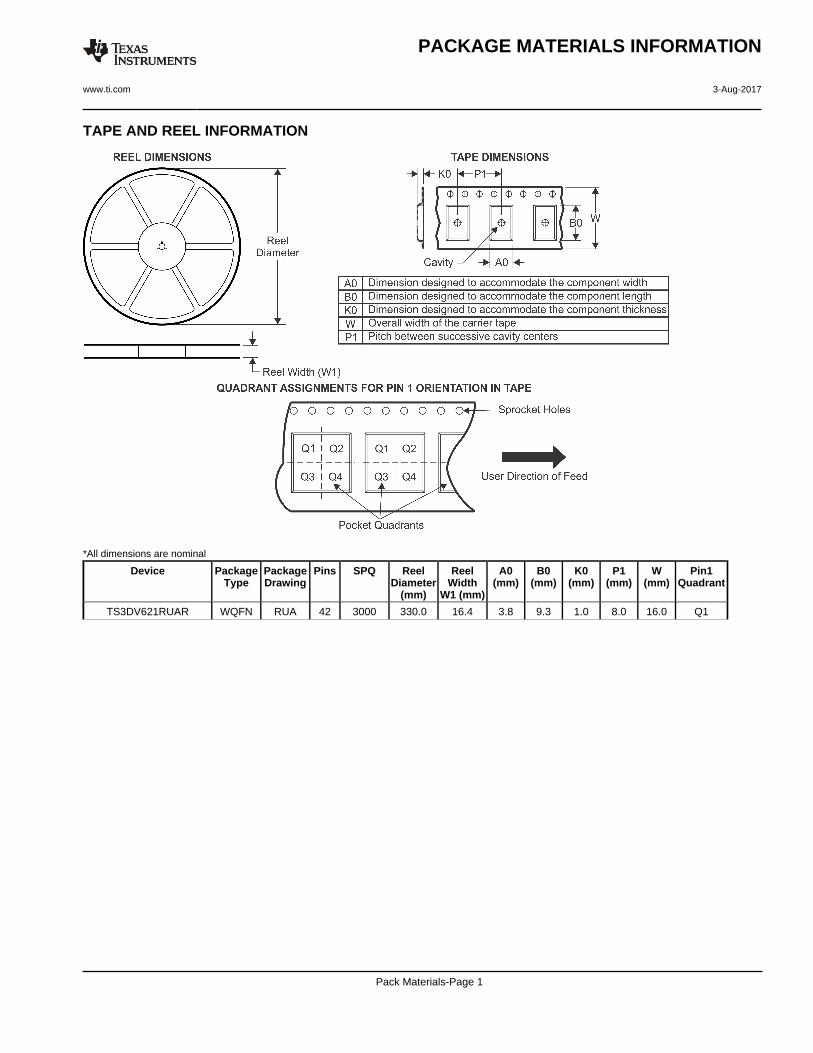
TAPE AND REEL INFORMATION
*All dimensions are nominal
Device PackageType
PackageDrawing
Pins SPQ ReelDiameter
(mm)
ReelWidth
W1 (mm)
A0(mm)
B0(mm)
K0(mm)
P1(mm)
W(mm)
Pin1Quadrant
TS3DV621RUAR WQFN RUA 42 3000 330.0 16.4 3.8 9.3 1.0 8.0 16.0 Q1
PACKAGE MATERIALS INFORMATION
www.ti.com 3-Aug-2017
Pack Materials-Page 1

*All dimensions are nominal
Device Package Type Package Drawing Pins SPQ Length (mm) Width (mm) Height (mm)
TS3DV621RUAR WQFN RUA 42 3000 358.0 335.0 35.0
PACKAGE MATERIALS INFORMATION
www.ti.com 3-Aug-2017
Pack Materials-Page 2


IMPORTANT NOTICE
Texas Instruments Incorporated (TI) reserves the right to make corrections, enhancements, improvements and other changes to itssemiconductor products and services per JESD46, latest issue, and to discontinue any product or service per JESD48, latest issue. Buyersshould obtain the latest relevant information before placing orders and should verify that such information is current and complete.TI’s published terms of sale for semiconductor products (http://www.ti.com/sc/docs/stdterms.htm) apply to the sale of packaged integratedcircuit products that TI has qualified and released to market. Additional terms may apply to the use or sale of other types of TI products andservices.Reproduction of significant portions of TI information in TI data sheets is permissible only if reproduction is without alteration and isaccompanied by all associated warranties, conditions, limitations, and notices. TI is not responsible or liable for such reproduceddocumentation. Information of third parties may be subject to additional restrictions. Resale of TI products or services with statementsdifferent from or beyond the parameters stated by TI for that product or service voids all express and any implied warranties for theassociated TI product or service and is an unfair and deceptive business practice. TI is not responsible or liable for any such statements.Buyers and others who are developing systems that incorporate TI products (collectively, “Designers”) understand and agree that Designersremain responsible for using their independent analysis, evaluation and judgment in designing their applications and that Designers havefull and exclusive responsibility to assure the safety of Designers' applications and compliance of their applications (and of all TI productsused in or for Designers’ applications) with all applicable regulations, laws and other applicable requirements. Designer represents that, withrespect to their applications, Designer has all the necessary expertise to create and implement safeguards that (1) anticipate dangerousconsequences of failures, (2) monitor failures and their consequences, and (3) lessen the likelihood of failures that might cause harm andtake appropriate actions. Designer agrees that prior to using or distributing any applications that include TI products, Designer willthoroughly test such applications and the functionality of such TI products as used in such applications.TI’s provision of technical, application or other design advice, quality characterization, reliability data or other services or information,including, but not limited to, reference designs and materials relating to evaluation modules, (collectively, “TI Resources”) are intended toassist designers who are developing applications that incorporate TI products; by downloading, accessing or using TI Resources in anyway, Designer (individually or, if Designer is acting on behalf of a company, Designer’s company) agrees to use any particular TI Resourcesolely for this purpose and subject to the terms of this Notice.TI’s provision of TI Resources does not expand or otherwise alter TI’s applicable published warranties or warranty disclaimers for TIproducts, and no additional obligations or liabilities arise from TI providing such TI Resources. TI reserves the right to make corrections,enhancements, improvements and other changes to its TI Resources. TI has not conducted any testing other than that specificallydescribed in the published documentation for a particular TI Resource.Designer is authorized to use, copy and modify any individual TI Resource only in connection with the development of applications thatinclude the TI product(s) identified in such TI Resource. NO OTHER LICENSE, EXPRESS OR IMPLIED, BY ESTOPPEL OR OTHERWISETO ANY OTHER TI INTELLECTUAL PROPERTY RIGHT, AND NO LICENSE TO ANY TECHNOLOGY OR INTELLECTUAL PROPERTYRIGHT OF TI OR ANY THIRD PARTY IS GRANTED HEREIN, including but not limited to any patent right, copyright, mask work right, orother intellectual property right relating to any combination, machine, or process in which TI products or services are used. Informationregarding or referencing third-party products or services does not constitute a license to use such products or services, or a warranty orendorsement thereof. Use of TI Resources may require a license from a third party under the patents or other intellectual property of thethird party, or a license from TI under the patents or other intellectual property of TI.TI RESOURCES ARE PROVIDED “AS IS” AND WITH ALL FAULTS. TI DISCLAIMS ALL OTHER WARRANTIES ORREPRESENTATIONS, EXPRESS OR IMPLIED, REGARDING RESOURCES OR USE THEREOF, INCLUDING BUT NOT LIMITED TOACCURACY OR COMPLETENESS, TITLE, ANY EPIDEMIC FAILURE WARRANTY AND ANY IMPLIED WARRANTIES OFMERCHANTABILITY, FITNESS FOR A PARTICULAR PURPOSE, AND NON-INFRINGEMENT OF ANY THIRD PARTY INTELLECTUALPROPERTY RIGHTS. TI SHALL NOT BE LIABLE FOR AND SHALL NOT DEFEND OR INDEMNIFY DESIGNER AGAINST ANY CLAIM,INCLUDING BUT NOT LIMITED TO ANY INFRINGEMENT CLAIM THAT RELATES TO OR IS BASED ON ANY COMBINATION OFPRODUCTS EVEN IF DESCRIBED IN TI RESOURCES OR OTHERWISE. IN NO EVENT SHALL TI BE LIABLE FOR ANY ACTUAL,DIRECT, SPECIAL, COLLATERAL, INDIRECT, PUNITIVE, INCIDENTAL, CONSEQUENTIAL OR EXEMPLARY DAMAGES INCONNECTION WITH OR ARISING OUT OF TI RESOURCES OR USE THEREOF, AND REGARDLESS OF WHETHER TI HAS BEENADVISED OF THE POSSIBILITY OF SUCH DAMAGES.Unless TI has explicitly designated an individual product as meeting the requirements of a particular industry standard (e.g., ISO/TS 16949and ISO 26262), TI is not responsible for any failure to meet such industry standard requirements.Where TI specifically promotes products as facilitating functional safety or as compliant with industry functional safety standards, suchproducts are intended to help enable customers to design and create their own applications that meet applicable functional safety standardsand requirements. Using products in an application does not by itself establish any safety features in the application. Designers mustensure compliance with safety-related requirements and standards applicable to their applications. Designer may not use any TI products inlife-critical medical equipment unless authorized officers of the parties have executed a special contract specifically governing such use.Life-critical medical equipment is medical equipment where failure of such equipment would cause serious bodily injury or death (e.g., lifesupport, pacemakers, defibrillators, heart pumps, neurostimulators, and implantables). Such equipment includes, without limitation, allmedical devices identified by the U.S. Food and Drug Administration as Class III devices and equivalent classifications outside the U.S.TI may expressly designate certain products as completing a particular qualification (e.g., Q100, Military Grade, or Enhanced Product).Designers agree that it has the necessary expertise to select the product with the appropriate qualification designation for their applicationsand that proper product selection is at Designers’ own risk. Designers are solely responsible for compliance with all legal and regulatoryrequirements in connection with such selection.Designer will fully indemnify TI and its representatives against any damages, costs, losses, and/or liabilities arising out of Designer’s non-compliance with the terms and provisions of this Notice.
Mailing Address: Texas Instruments, Post Office Box 655303, Dallas, Texas 75265Copyright © 2017, Texas Instruments Incorporated