Embed Size (px)
Citation preview

HAL Id: hal-01430910https://hal.archives-ouvertes.fr/hal-01430910
Submitted on 31 Jan 2017
HAL is a multi-disciplinary open accessarchive for the deposit and dissemination of sci-entific research documents, whether they are pub-lished or not. The documents may come fromteaching and research institutions in France orabroad, or from public or private research centers.
L’archive ouverte pluridisciplinaire HAL, estdestinée au dépôt et à la diffusion de documentsscientifiques de niveau recherche, publiés ou non,émanant des établissements d’enseignement et derecherche français ou étrangers, des laboratoirespublics ou privés.
Scattering of electrically excited surface plasmonpolaritons by gold nanoparticles studied by optical
interferometry with a scanning tunneling microscopeTao Wang, Benoît Rogez, Geneviève Comtet, Eric Le Moal, Wafa Abidi, Hynd
Remita, Gérald Dujardin, Elizabeth Boer-Duchemin
To cite this version:Tao Wang, Benoît Rogez, Geneviève Comtet, Eric Le Moal, Wafa Abidi, et al.. Scattering of electricallyexcited surface plasmon polaritons by gold nanoparticles studied by optical interferometry with ascanning tunneling microscope. Physical Review B: Condensed Matter and Materials Physics (1998-2015), American Physical Society, 2015, 92 (23), pp.45438 - 45438. �10.1103/PhysRevB.92.045438�.�hal-01430910�

PHYSICAL REVIEW B 92, 045438 (2015)
Scattering of electrically excited surface plasmon polaritons by gold nanoparticles studied by opticalinterferometry with a scanning tunneling microscope
Tao Wang,1,* Benoıt Rogez,1 Genevieve Comtet,1 Eric Le Moal,1,† Wafa Abidi,2 Hynd Remita,2
Gerald Dujardin,1 and Elizabeth Boer-Duchemin1
1Institut des Sciences Moleculaires d’Orsay, CNRS–Universite Paris-Sud (UMR 8214), Orsay, France2Laboratoire de Chimie Physique, CNRS–Universite Paris-Sud (UMR 8000), Orsay, France
(Received 9 March 2015; revised manuscript received 17 April 2015; published 31 July 2015)
We study the scattering of electrically excited surface plasmon polaritons (SPP) from individual nanostructures.The tunneling electrons from a scanning tunneling microscope (STM) are used to excite an out-going, circularSPP wave on a thin (50-nm) gold film on which isolated gold nanoparticles (NPs) have been deposited. Interactionof the excited SPPs with the NPs leads to both in-plane (SPP-to-SPP) and out-of-plane (SPP-to-photon) scattering.We use SPP leakage radiation microscopy to monitor the interference between the incident and in-plane scatteredSPP waves in the image plane. By changing the location of the STM tip, the distance of the pointlike SPP sourceto the scatterers can be varied at will, which constitutes a key advantage over other existing techniques. Aswell, the out-of-plane scattered radiation interferes with the direct light emission from the STM tip in the backfocal plane (Fourier plane). This confirms the mutual coherence of the light and SPP emission resulting fromthe inelastic tunneling of an electron in the STM junction. We use this effect to demonstrate that SPP-to-photonscattering at NPs is highly directional.
DOI: 10.1103/PhysRevB.92.045438 PACS number(s): 73.20.Mf, 68.37.Ef, 78.67.Bf
I. INTRODUCTION
Surface plasmon polaritons (SPPs), i.e., electromagneticwaves propagating on a metallic surface, are considered key el-ements for the integration of optics with nanoelectronics [1–5].In plasmonic circuitry, SPP propagation can be controlled viain-plane SPP-to-SPP scattering on a nanostructured metallicsurface [6–8]. Efficient scatterers such as metal nanoparticles(NPs) may be assembled in periodic arrays to form micro-optical components for SPPs, e.g., mirrors, beam splitters, andlenses [9–13]. Importantly for optoelectronics applications,out-of-plane SPP-to-photon scattering at NPs may be used toengineer the coupling between SPPs and light [14,15].
Several experimental studies on the NP-scattering ofSPPs have been reported [16–25], most of them based onscanning near field optical microscopy (SNOM) [16–23].Crucial aspects such as coherence conservation and phaseshifts upon SPP scattering by metal NPs have, however,rarely been probed so far. As well, the angular distributionof out-of-plane SPP scattering is an important observable thatis often not accessible in the reported experimental approaches.Cathodoluminescence (CL) imaging techniques have beendeveloped to angularly resolve the light emission from singlegold nanodisks [26] or nanoholes [27] upon direct excitationof their plasmonic modes with a high-energy electron beam;yet, this technique has not been applied to the study of thescattering of propagating SPPs by a single nanostructure.A high-energy electron beam has also been used to excitepropagating SPPs directly on unstructured metal surfaces andout-coupled into photons using a grating, thus leading to ameasurement of the plasmon propagation length [28,29]. Aswell, phase-sensitive SNOM (P-SNOM) techniques have been
*Present address: Department of Chemistry, NUS 3 Science Drive3, Singapore 117543.
†Corresponding author: [email protected]
used to characterize the response of a hole etched in a thick goldfilm to incident SPP plane waves [30,31]. Complex-amplitudenearfield images are measured by raster scanning a nearfielddetection probe and the angular distribution of both the SPPand light fields can in principle be retrieved by computing theFourier transform of these images; however, the influence ofthe nearfield probe has been shown to introduce artifacts [30].So far, no P-SNOM study of SPP scattering by a NP hasbeen reported. A widefield imaging mode where the wholeregion of interest is imaged simultaneously is ideal for thestudy of NP scattering of SPPs. In conjunction with localSPP excitation, widefield imaging may be used to monitor thespatial distribution of the extended SPP modes as well as theirinterplay with local scatterers [11,18]. Photoemission electronmicroscopy (PEEM) is also a technique that has widefieldimaging capabilities. An interferometric time-resolved tech-nique derived from PEEM has recently been used to study theinteraction of SPPs with gold nanodots [25]. In this technique,the SPP waves are optically generated by coupling light fromthe far field to a fixed step edge on the gold surface. In thisconfiguration, SPP scattering at a given nanostructure canonly be characterized for a single direction of SPP incidenceand a single SPP source-nanodot distance (virtually infinitysince SPP plane waves are generated). Moreover, in-planeand out-of-plane SPP scattering cannot be distinguished withPEEM.
In this article, we combine optical and scanning tunnelingmicroscopy (STM) to study the SPP scattering propertiesof individual nanostructures. This technique combines theadvantages of a local SPP source (like SNOM and CL) andwidefield optical imaging. Such an experimental approach hasrecently been used to study SPP scattering at the end of a goldnanowire [32], at the edges of a gold nanostripe [33], at holesetched in a gold film [34,35], and at the slits of linear [36] andcircular gratings [37]; yet this approach has never been used tostudy the interaction of 2D SPPs with a single 0D NP. In thisexperiment, we use the inelastic tunneling of electrons from
1098-0121/2015/92(4)/045438(7) 045438-1 ©2015 American Physical Society

TAO WANG et al. PHYSICAL REVIEW B 92, 045438 (2015)
e-STM tip
glass
gold film
gold NP
SPP
SPP scattering
10 μm 10 μm
10 μm 10 μm
AF
M h
eigh
t(nm
)
0
500(b)
(d) (e)
(c)
(NA = 1.45) (NA = 0.75)
(darkfield)
STM �p STM �p
(a)
FIG. 1. (Color online) (a) Schematic of the experiment: goldnanoparticles (NPs) are dispersed on a thin gold film depositedon a glass coverslip. Inelastic electron tunneling from the STMtip to the gold film electrically excites surface plasmon polaritons(SPPs) that propagate isotropically away from the tunnel junction.SPP-to-SPP scattering at the gold NPs is imaged by leakage radiationmicroscopy (LRM), using an inverted optical microscope coupledto the STM. (b) Darkfield optical microscopy image of gold NPsdispersed on the gold film. This image is obtained using an airobjective of numerical aperture NA = 0.75 upon illumination of thesample with a collimated white light beam at grazing incidence.(c) Atomic force microscopy (AFM) image of the same area as in (b).(d) Gray-scale optical LRM image of the same area during STM-SPPexcitation, obtained using an oil-immersion objective of NA = 1.45.The location of the STM tip on the gold film is indicated by thered arrow. (e) Same as in (d) but obtained using an air objectiveof NA = 0.75. Such an objective cannot collect the SPP leakageradiation.
the STM tip as a nanosource of circular SPP waves on a thingold film [32,38]. These waves propagate away from the tiplocation and scatter at gold NPs on the gold film [see Fig. 1(a)].Two different elastic-scattering processes may occur: in-planeSPP-to-SPP scattering (NPs act as secondary sources ofSPPs) and out-of-plane SPP-to-photon scattering [21]. Bothprocesses are investigated by monitoring the light transmittedthrough the substrate, which is collected using a microscopeobjective and imaged on a cooled charge-coupled devicecamera. The interference between the incident and in-planescattered SPPs is recorded by imaging the leakage radiationin real space (spatial distribution) [18,39]. In Fourier space(angular distribution), we examine the optical interferencebetween the scattering radiation from the NPs and the lightdirectly emitted from the STM tip. We find that SPPs scattered
out-of-plane by gold NPs are highly forward scattered. Finally,our results demonstrate that all the emission and scatteringprocesses at play, namely the light and SPP emission from theSTM tip and the in-plane and out-of-plane scattering at theNPs, are mutually coherent.
II. METHODS
We use an STM-AFM (atomic force microscope) head(Veeco Bioscope/Nanoscope IVa) mounted onto an invertedoptical microscope (Zeiss Axiovert). A nanopositioning stagecontrols the lateral position of the sample with respect tothe STM tip, which is an electrochemically etched tungstenwire. Gold NPs (mean diameter 150 nm) stabilized by cyanideligands are synthesized using a seed-mediated method byradiolysis [40] and drop casted onto a thin gold film (thickness50 nm) thermally evaporated on a glass coverslip. The sampleis biased to 2.8 V with respect to the tip and the setpoint tunnelcurrent is 6 nA.
III. RESULTS AND DISCUSSION
Figure 1 illustrates the principle of our approach andhighlights its advantages for the study of SPP scattering. Priorto STM experiments, we detect and identify the same goldNPs on the gold film by both darkfield optical microscopy[see Fig. 1(b)] and tapping-mode AFM [see Fig. 1(c)].Subsequently, we use the STM tip to generate a pointlikesource [34] of 2D circular SPPs in the same region of interest.Figure 1(d) shows the real-space image obtained with anoil-immersion objective (NA = 1.45, θmax = 72◦ in glass).With such an objective, the SPP leakage radiation from theair-gold interface, which is emitted at an angle that is slightlylarger than the air-glass critical angle (θc = 41◦), is collected.The coherent superposition of the incident and scattered SPPwaves generates a hyperbolic dark “shadow” just after thegold NPs [see Fig. 1(d)]. Figure 1(e) shows the real-spaceimage measured under the same conditions but with an airobjective (NA = 0.75, θmax = 30◦ in glass), whose numericalaperture is too low to collect the SPP leakage radiation. Brightspots are seen at the location of the gold NPs since the lightfrom SPP out-of-plane scattering is emitted at all angles. Thepresence of an intense spot at the tip location is not due tosecondary scattering of back-scattered SPP waves at the tipbut results from the fact that the tunnel junction behaves asboth a nanosource of SPPs and photons. This is expected sinceSTM-induced light emission is often described as the radiationof a vertical electric dipole inside the tunnel junction [41].Close to a thin gold film on glass, a vertical electric dipolecouples naturally to both SPPs bound to the air-gold interfaceas well as to free-space radiation in air and glass.
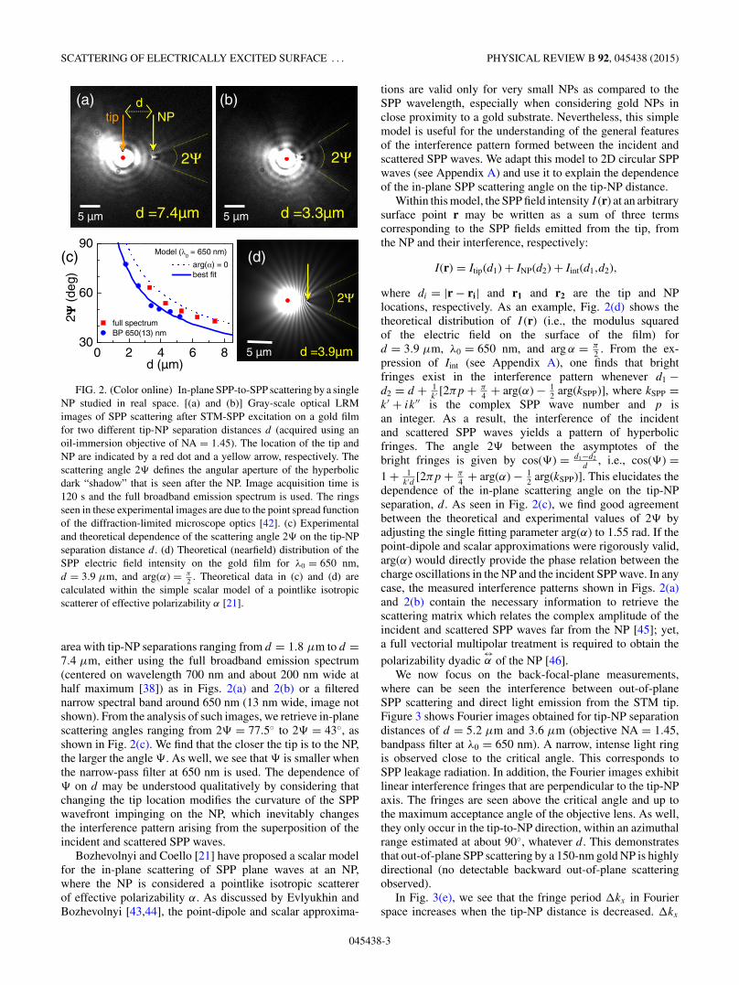
In the following we report on experiments involving asingle, isolated NP. Figure 2 shows that a hyperbolic dark“shadow” forms in the real-space image when SPPs elasticallyscatter into SPPs at a gold NP. This feature is particularlyinteresting because it is related to the phase shift betweenthe incident and scattered SPP waves. As well, the tip-NPdistance d has a strong effect on the in-plane scatteringangle 2�, i.e., the angular aperture of the “shadow” afterthe NP. We measure several real-space images of the same
045438-2
SCATTERING OF ELECTRICALLY EXCITED SURFACE . . . PHYSICAL REVIEW B 92, 045438 (2015)
(c)
0 2 4 6 830
60
90
full spectrumBP 650(13) nm
Model (λ0 = 650 nm)
arg(α) = 0 best fit
2 ΨΨ ΨΨ (
deg)
d (µm)
2Ψ
5 µm 5 µmd =7.4µm d =3.3µm
(a) (b)
2Ψ
NPtipd
5 µm
2Ψ
d =3.9µm
(d)
FIG. 2. (Color online) In-plane SPP-to-SPP scattering by a singleNP studied in real space. [(a) and (b)] Gray-scale optical LRMimages of SPP scattering after STM-SPP excitation on a gold filmfor two different tip-NP separation distances d (acquired using anoil-immersion objective of NA = 1.45). The location of the tip andNP are indicated by a red dot and a yellow arrow, respectively. Thescattering angle 2� defines the angular aperture of the hyperbolicdark “shadow” that is seen after the NP. Image acquisition time is120 s and the full broadband emission spectrum is used. The ringsseen in these experimental images are due to the point spread functionof the diffraction-limited microscope optics [42]. (c) Experimentaland theoretical dependence of the scattering angle 2� on the tip-NPseparation distance d . (d) Theoretical (nearfield) distribution of theSPP electric field intensity on the gold film for λ0 = 650 nm,d = 3.9 μm, and arg(α) = π
2 . Theoretical data in (c) and (d) arecalculated within the simple scalar model of a pointlike isotropicscatterer of effective polarizability α [21].
area with tip-NP separations ranging from d = 1.8 μm to d =7.4 μm, either using the full broadband emission spectrum(centered on wavelength 700 nm and about 200 nm wide athalf maximum [38]) as in Figs. 2(a) and 2(b) or a filterednarrow spectral band around 650 nm (13 nm wide, image notshown). From the analysis of such images, we retrieve in-planescattering angles ranging from 2� = 77.5◦ to 2� = 43◦, asshown in Fig. 2(c). We find that the closer the tip is to the NP,the larger the angle �. As well, we see that � is smaller whenthe narrow-pass filter at 650 nm is used. The dependence of� on d may be understood qualitatively by considering thatchanging the tip location modifies the curvature of the SPPwavefront impinging on the NP, which inevitably changesthe interference pattern arising from the superposition of theincident and scattered SPP waves.
Bozhevolnyi and Coello [21] have proposed a scalar modelfor the in-plane scattering of SPP plane waves at an NP,where the NP is considered a pointlike isotropic scattererof effective polarizability α. As discussed by Evlyukhin andBozhevolnyi [43,44], the point-dipole and scalar approxima-
tions are valid only for very small NPs as compared to theSPP wavelength, especially when considering gold NPs inclose proximity to a gold substrate. Nevertheless, this simplemodel is useful for the understanding of the general featuresof the interference pattern formed between the incident andscattered SPP waves. We adapt this model to 2D circular SPPwaves (see Appendix A) and use it to explain the dependenceof the in-plane SPP scattering angle on the tip-NP distance.
Within this model, the SPP field intensity I (r) at an arbitrarysurface point r may be written as a sum of three termscorresponding to the SPP fields emitted from the tip, fromthe NP and their interference, respectively:
I(r) = Itip(d1) + INP(d2) + Iint(d1,d2),
where di = |r − ri| and r1 and r2 are the tip and NPlocations, respectively. As an example, Fig. 2(d) shows thetheoretical distribution of I (r) (i.e., the modulus squaredof the electric field on the surface of the film) ford = 3.9 μm, λ0 = 650 nm, and arg α = π
2 . From the ex-pression of Iint (see Appendix A), one finds that brightfringes exist in the interference pattern whenever d1 −d2 = d + 1
k′ [2πp + π4 + arg(α) − 1
2 arg(kSPP)], where kSPP =k′ + ik′′ is the complex SPP wave number and p isan integer. As a result, the interference of the incidentand scattered SPP waves yields a pattern of hyperbolicfringes. The angle 2� between the asymptotes of thebright fringes is given by cos(�) = d1−d2
d, i.e., cos(�) =
1 + 1k′d [2πp + π
4 + arg(α) − 12 arg(kSPP)]. This elucidates the
dependence of the in-plane scattering angle on the tip-NPseparation, d. As seen in Fig. 2(c), we find good agreementbetween the theoretical and experimental values of 2� byadjusting the single fitting parameter arg(α) to 1.55 rad. If thepoint-dipole and scalar approximations were rigorously valid,arg(α) would directly provide the phase relation between thecharge oscillations in the NP and the incident SPP wave. In anycase, the measured interference patterns shown in Figs. 2(a)and 2(b) contain the necessary information to retrieve thescattering matrix which relates the complex amplitude of theincident and scattered SPP waves far from the NP [45]; yet,a full vectorial multipolar treatment is required to obtain the
polarizability dyadic↔α of the NP [46].
We now focus on the back-focal-plane measurements,where can be seen the interference between out-of-planeSPP scattering and direct light emission from the STM tip.Figure 3 shows Fourier images obtained for tip-NP separationdistances of d = 5.2 μm and 3.6 μm (objective NA = 1.45,bandpass filter at λ0 = 650 nm). A narrow, intense light ringis observed close to the critical angle. This corresponds toSPP leakage radiation. In addition, the Fourier images exhibitlinear interference fringes that are perpendicular to the tip-NPaxis. The fringes are seen above the critical angle and up tothe maximum acceptance angle of the objective lens. As well,they only occur in the tip-to-NP direction, within an azimuthalrange estimated at about 90◦, whatever d. This demonstratesthat out-of-plane SPP scattering by a 150-nm gold NP is highlydirectional (no detectable backward out-of-plane scatteringobserved).
In Fig. 3(e), we see that the fringe period �kx in Fourierspace increases when the tip-NP distance is decreased. �kx
045438-3

TAO WANG et al. PHYSICAL REVIEW B 92, 045438 (2015)
d=5.2µm d=3.6µm
(a) (b)
2 3 4 5 60
1
0.4
0.6
0.8
1.0
Inte
nsity
max
, Im
ax
d (µm)
Model: Sc. 1 Sc. 2
Visibility, V
d
I0 SPP I1
σ2I2 σ1I1
STM tip gold NPd
air
glass
I0 SPP I1
ΓI0 σ1I1I2
θ θ
Sc. 1 Sc. 2(c) (d)
(e) (f)
2 3 4 5 6
0.1
0.2
0.3
Frin
ge p
erio
d, Δ
k x / k 0
d (µm)
Model Δk
x / k
0 = λ
0/ d
λ0 = 650nm
Experiment
FIG. 3. (Color online) Out-of-plane SPP-to-photon scattering bya single NP studied in Fourier space. [(a) and (b)] Gray-scaleoptical LRM images measured in Fourier space for two differenttip-NP distances (exposure time: 120 s, bandpass filter at λ0 =650 nm). The red dashed arrow indicates the tip-to-NP direction.[(c) and (d)] Schematics of two possible scenarios that may explainthe interference fringes observed in Fourier space (see the text forparameter definitions). [(e) and (f)] Experimental and theoreticaldependence of (e) the fringe period, (f) maximal intensity (blacksquares), and visibility (magenta dots) on the tip-NP separation d .The distance dependence of Imax validates scenario 1 and rules outscenario 2.
closely follows a �kx/k0 = λ0/d rule, which is typical of theinterference of light from two pointlike coherent sources [34].The two coherent light sources are the tunnel junction andthe NP; yet two possible scenarios (or propagation paths)may explain our observations, as illustrated in Figs. 3(c)and 3(d). In scenario 1 (Sc. 1), out-of-plane forward SPPscattering at the NP interferes with the directly emittedlight from the tunnel junction. In scenario 2 (Sc. 2) theout-of-plane forward SPP scattering at the NP interferes withthe SPP wave that has been scattered twice: first at the NP(in-plane backward scattering) and then at the tip (out-of-planebackward scattering). Importantly, Sc. 1 requires that theplasmonic and photonic emission of the tunnel junction be
mutually coherent, whereas Sc. 2 does not, since it involvesthe same SPP that is elastically and coherently scattered in theplane. We propose below a simple method to determine thecorrect scenario, which takes advantage of the fact that we caneasily vary the tip-NP distance.
We define I0 as the initial intensity of the electric fieldat the STM-tip nanosource, I1 as the intensity at the NPafter SPP propagation from the tip, and I2 as the intensityat the tip after SPP propagation back from the NP. In Fourierspace, the intensity of the interference fringes is I (kx) = �I0 +σ1I1 + 2
√�I0σ1I1 cos (kxd + �φ1) in Sc. 1 and I (kx) =
σ1I1 + σ2I2 + 2√
σ1I1σ2I2 cos (kxd + �φ2) in Sc. 2, where� is the relative efficiency of the light emitted directly by theSTM-nanosource in the substrate, σi is the out-of-plane SPPscattering efficiency at the NP (i = 1) or at the tip (i = 2),and �φi is the phase shift due to SPP propagation [35]and out-of-plane scattering. As a result, the intensity of thebright and dark fringes is Imax/min = �I0 + σ1I1 ± 2
√�I0σ1I1
in Sc. 1 and Imax/min = σ1I1 + σ2I2 ± 2√
σ1I1σ2I2 in Sc. 2,respectively. We note V = Imax−Imin
Imax+Iminthe visibility of the fringe
pattern. In Fig. 3(f), we plot the experimental values ofImax and V versus d and fit them with their theoreticalexpressions (fitting parameters are I0, �, and σi). I1 and I2
are calculated by assuming emission of cylindrical, scalar SPPwaves from the tip and NP locations (see Appendix B). It isclear in Fig. 3(f) that very good agreement between experimentand theory is similarly obtained for V in both scenarios.However, Imax varies quite differently with the tip-NP distance
d; indeed, Imax = �I0(1 +√
η1
de−k′′d )
2in Sc. 1, whereas in
Sc. 2 Imax = σ1I0e−2k′′d
d(1 +
√η2
de−k′′d )
2where ηi (i = 1,2)
is a constant (see Appendix B). As seen in Fig. 3(f), Imax
closely reproduces the experimental observations in Sc. 1,unlike in Sc. 2 (whose least-squares fit leads to value ofσ2 = 0). Therefore Sc. 2 may be ruled out and the scenariowhere the SPPs scattered at the NP interfere with the lightdirectly emitted by the tunnel junction is validated. Theseresults are conclusive evidence that the plasmonic and photonicemission channels of the tunnel junction are coherent. Ourobservations also verify that this coherence is preserved whenthe propagating SPPs are converted into photons upon elasticscattering at a nanostructure, otherwise no interference wouldoccur in the Fourier plane.
IV. CONCLUSION
To conclude, we combine STM with optical microscopy tostudy the SPP scattering properties of gold NPs on a gold film.Electrically excited SPPs are launched from the tunnel junctionof an STM, yielding an isotropic nanosource of circular SPPwaves. This approach provides both the advantages of a local,electrical SPP excitation with a widefield optical imagingmode. In this way, the spatial distribution of the extendedSPP modes and their interaction with localized scatterers maybe monitored. The SPP STM-nanosource can be moved toany point on the gold surface that is accessible by STM, unlikeother techniques which use a fixed defect or grating to opticallyexcite SPPs. We study how the distance d between the SPPnanosource and a single NP affects the interference pattern
045438-4

SCATTERING OF ELECTRICALLY EXCITED SURFACE . . . PHYSICAL REVIEW B 92, 045438 (2015)
that forms in real and Fourier-space images. In real space,hyperbolic fringes arise from the coherent superposition of theincident and in-plane scattered SPP waves which are detectedvia SPP leakage radiation. In Fourier space, linear fringesare observed at supercritical angles in the tip-to-NP direction,due to the directionality of the out-of-plane scattering atthe NP. The fringe period dependence on d demonstratesthat the SPPs radiatively scattered at the NP interfere withthe light directly emitted from the tunnel junction. Thus,we experimentally demonstrate the mutual coherence of thephotonic and plasmonic emission from the inelastic tunnelingof an electron in the STM junction.
The mutual coherence of the SPP and light emissionresulting from the inelastic tunneling of an electron throughthe tunnel junction is a direct consequence of the wave natureof SPPs and photons. Electron tunneling is indeed a stochasticprocess and no coherence is expected between two successivetunneling events. From a classical point of view, we maythus consider that one single inelastic electron tunneling eventyields an electromagnetic wave that simultaneously propagatesalong the air-gold interface and in the glass substrate, i.e., awave that has both plasmonic and photonic character.
These STM-based interferometric measurements may beused in future work to monitor SPP coherence losses andphase shifts in more complicated systems, including semi-continuous metallic films [47,48] and hybrid systems whereSPPs are strongly coupled to the excitons of semiconductornanostructures [49,50].
ACKNOWLEDGMENTS
This work was supported by Agence Nationale de laRecherche through project NAPHO (Contract No. ANR-08-NANO-054) and by the European Commission through theSeventh Framework Programme (FP7-ICT-2009, Contract No.243421). We thank C. Girard, J.-J. Greffet, and J.-P. Hugoninfor fruitful discussions.
APPENDIX A: MODEL FOR IN-PLANE(SPP-TO-SPP) SCATTERING
In order to understand the general features of the interfer-ence pattern of the incident and scattered SPP waves, we use ascalar model first proposed by Bozhevolnyi and Coello for thescattering of SPP plane waves [21]. Here we adapt this modelto 2D circular SPP waves. The NP is considered a pointlikeisotropic scatterer of effective polarizability α. The scalar SPPfield E(r) at an arbitrary surface point r is the coherent sumof the isotropic SPP emission from the tunnel junction andthe scattered SPP field from the NP. Within a 0th-order Bornapproximation, E(r) may be written
E(r) = E0(|r − r1|) + αE0(|r2 − r1|)G(|r − r2|),where r1 and r2 are the tip and NP locations, respectively. Thecylindrical field propagating away from the tip is
E0(|r − r1|) = eikSPP|r−r1|/√
|r − r1|,where kSPP = k′ + ik′′ is the complex SPP wave number. Thepropagator G is proportional to the 0th-order Hankel function
of the first type H(1)0 :
G(r,r2) = i
4H
(1)0 (kSPPd2),
where di = |r − ri|. H(1)0 (x) tends asymptotically to√
2πx
ei(x− π4 ) for x � 1; [51] hence, far enough away from
the NP (as compared to the SPP wavelength), the SPP fieldmay be written:
E(r) = eikSPPd1/√
d1 + A2eikSPPd2/
√d2,
where A2 = α4
√2
πkSPPdei(kSPPd+ π
4 ) and d = |r2 − r1|. Thus theSPP field intensity I (r) = E(r)E∗(r) may be written as a sumof three terms corresponding to the SPP fields emitted fromthe tip, from the NP and their interference, respectively, asfollows:
I(r) = Itip(d1) + INP(d2) + Iint(d1,d2), (A1)
Itip(d1) = e−2k′′d1
d1, (A2)
INP(d2) = |α|28π |kSPP|dd2
e−2k′′(d+d2), (A3)
Iint(d1,d2) = |α|√2π |kSPP|dd1d2
e−k′′(d1+d2+d)
cos
[k′(d1 − d2 − d) − π
4− arg (α) + 1
2arg (kSPP)
]. (A4)
As an example, Fig. 2(d) in the main article shows thetheoretical distribution of I (r) for d = 3.9 μm, λ0 = 650 nm,and arg(α) = π
2 . Bright fringes exist in the interferencepattern when the cosine in Eq. (A4) equals 1, i.e., wheneverd1 − d2 = d + 1
k′ [2πp + π4 + arg(α) − 1
2 arg(kSPP)] where p
is an integer. As a result, the interference of the incident andscattered SPP waves yields a pattern of hyperbolic fringes. Theangle 2� between the asymptotes of the bright fringes is givenby cos(�) = d1−d2
d, i.e.,
cos(�) = 1 + 1
k′d
[2πp + π
4+ arg(α) − 1
2arg(kSPP)
].
APPENDIX B: MODEL FOR OUT-OF-PLANE(SPP-TO-PHOTON) SCATTERING
From Eqs. (A2) and (A3), the intensity I1 at the NP afterSPP propagation from the tip and the intensity I2 at the tipafter SPP propagation back from the NP read:
I1 = I0
de−2k′′d
I2 = |α|2I0
8π |kSPP|d2e−4k′′d ,
where I0 is the initial intensity of the electric field at theSTM-tip nanosource.
The visibility of the fringe pattern in Fourier space reads:
V = Imax − Imin
Imax + Imin.
045438-5

TAO WANG et al. PHYSICAL REVIEW B 92, 045438 (2015)
The variation of V with d is the same in the twoscenarios described in Figs. 3(c) and 3(d) (Sc. 1 and Sc. 2);indeed,
V = 2
√ηi
d
e−k′′d
1 + ηi
de−2k′′d ,
where η1 = σ1�
in Sc. 1 and η2 = |α|2σ2
8π |kSPP|σ1in Sc. 2.
Conversely, Imax varies quite differently with the tip-NPdistance d, namely
Imax,Sc.1 = �I0
(1 +
√η1
de−k′′d
)2
Imax,Sc.2 = σ1I0e−2k′′d
d
(1 +
√η2
de−k′′d
)2
.
[1] E. Ozbay, Science 311, 189 (2006).[2] H. A. Atwater, Sci. Am. 296, 56 (2007).[3] K. F. MacDonald, Z. L. Samson, M. I. Stockman, and N. I.
Zheludev, Nat. Photon. 3, 55 (2009).[4] D. K. Gramotnev and S. I. Bozhevolnyi, Nat. Photon. 4, 83
(2010).[5] V. J. Sorger, R. F. Oulton, R.-M. Ma, and X. Zhang, MRS Bull.
37, 728 (2012).[6] E. Devaux, T. W. Ebbesen, J.-C. Weeber, and A. Dereux,
Appl. Phys. Lett. 83, 4936 (2003).[7] T. W. Ebbesen, C. Genet, and S. I. Bozhevolnyi, Phys. Today
61, 44 (2008).[8] E. Devaux, J.-Y. Laluet, B. Stein, C. Genet, T. Ebbesen, J.-C.
Weeber, and A. Dereux, Opt. Express 18, 20610 (2010).[9] H. Ditlbacher, J. R. Krenn, G. Schider, A. Leitner, and F. R.
Aussenegg, Appl. Phys. Lett. 81, 1762 (2002).[10] J. R. Krenn, H. Ditlbacher, G. Schider, A. Hohenau, A. Leitner,
and F. R. Aussenegg, J. Microsc. 209, 167 (2003).[11] A. Drezet, A. Hohenau, A. L. Stepanov, H. Ditlbacher, B.
Steinberger, F. R. Aussenegg, A. Leitner, and J. R. Krenn,Plasmonics 1, 141 (2006).
[12] A. B. Evlyukhin, S. I. Bozhevolnyi, A. L. Stepanov, R. Kiyan,C. Reinhardt, S. Passinger, and B. N. Chichkov, Opt. Express15, 16667 (2007).
[13] I. P. Radko, A. B. Evlyukhin, A. Boltasseva, and S. I.Bozhevolnyi, Opt. Express 16, 3924 (2008).
[14] H. A. Atwater and A. Polman, Nat. Mater. 9, 205(2010).
[15] C. M. Chang, M. L. Tseng, B. H. Cheng, C. H. Chu, Y. Z. Ho,H. W. Huang, Y.-C. Lan, D.-W. Huang, A. Q. Liu, and D. P.Tsai, Adv. Mater. 25, 1118 (2013).
[16] S. I. Bozhevolnyi, I. I. Smolyaninov, and A. V. Zayats,Phys. Rev. B 51, 17916 (1995).
[17] I. I. Smolyaninov, D. L. Mazzoni, and C. C. Davis, Phys. Rev.Lett. 77, 3877 (1996).
[18] B. Hecht, H. Bielefeldt, L. Novotny, Y. Inouye, and D. W. Pohl,Phys. Rev. Lett. 77, 1889 (1996).
[19] L. Novotny, B. Hecht, and D. W. Pohl, J. Appl. Phys. 81, 1798(1997).
[20] J. Krenn, R. Wolf, A. Leitner, and F. Aussenegg, Opt. Commun.137, 46 (1997).
[21] S. I. Bozhevolnyi and V. Coello, Phys. Rev. B 58, 10899 (1998).[22] B. Vohnsen and S. I. Bozhevolnyi, Appl. Opt. 40, 6081 (2001).[23] A. L. Stepanov, J. R. Krenn, H. Ditlbacher, A. Hohenau,
A. Drezet, B. Steinberger, A. Leitner, and F. R. Aussenegg,Opt. Lett. 30, 1524 (2005).
[24] J. K. Day, O. Neumann, N. K. Grady, and N. J. Halas,ACS Nano 4, 7566 (2010).
[25] C. Lemke, T. Leiner, A. Evlyukhin, J. W. Radke, A. Klick,J. Fiutowski, J. Kjelstrup-Hansen, H.-G. Rubahn, B. N.Chichkov, C. Reinhardt, and M. Bauer, Nano Lett. 14, 2431(2014).
[26] T. Coenen, F. Bernal Arango, A. Femius Koenderink, andA. Polman, Nat. Comm. 5 (2014).
[27] T. Coenen and A. Polman, ACS Nano 8, 7350 (2014).[28] M. V. Bashevoy, F. Jonsson, A. V. Krasavin, N. I. Zheludev, Y.
Chen, and M. I. Stockman, Nano Lett. 6, 1113 (2006).[29] J. T. van Wijngaarden, E. Verhagen, A. Polman, C. E. Ross, H. J.
Lezec, and H. A. Atwater, Appl. Phys. Lett. 88, 221111 (2006).[30] N. Rotenberg, M. Spasenovic, T. L. Krijger, B. le Feber, F. J.
Garcıa de Abajo, and L. Kuipers, Phys. Rev. Lett. 108, 127402(2012).
[31] N. Rotenberg, T. L. Krijger, B. le Feber, M. Spasenovic, F. J. deAbajo, and L. Kuipers, Phys. Rev. B 88, 241408(R) (2013).
[32] P. Bharadwaj, A. Bouhelier, and L. Novotny, Phys. Rev. Lett.106, 226802 (2011).
[33] Y. Zhang, E. Boer-Duchemin, T. Wang, B. Rogez, G. Comtet, E.Le Moal, G. Dujardin, A. Hohenau, C. Gruber, and J. R. Krenn,Opt. Express 21, 13938 (2013).
[34] T. Wang, E. Boer-Duchemin, G. Comtet, E. Le Moal, G.Dujardin, A. Drezet, and S. Huant, Nanotechnology 25, 125202(2014).
[35] T. Wang, G. Comtet, E. Le Moal, G. Dujardin, A. Drezet, S.Huant, and E. Boer-Duchemin, Opt. Lett. 39, 6679 (2014).
[36] Z. Dong, H.-S. Chu, D. Zhu, W. Du, Y. A. Akimov, W. P. Goh,T. Wang, K. E. J. Goh, C. Troadec, C. A. Nijhuis, and J. K. W.Yang, ACS Photon. 2, 385 (2015).
[37] S. Cao, E. Le Moal, E. Boer-Duchemin, G. Dujardin, A. Drezet,and S. Huant, Appl. Phys. Lett. 105, 111103 (2014).
[38] T. Wang, E. Boer-Duchemin, Y. Zhang, G. Comtet, andG. Dujardin, Nanotechnology 22, 175201 (2011).
[39] A. Bouhelier, T. Huser, H. Tamaru, H.-J. Guntherodt, D. W.Pohl, F. I. Baida, and D. Van Labeke, Phys. Rev. B 63, 155404(2001).
[40] W. Abidi and H. Remita, Recent Pat. Eng. 4, 170 (2010).[41] P. Johansson, R. Monreal, and P. Apell, Phys. Rev. B 42, 9210
(1990).[42] A. Hohenau, J. R. Krenn, A. Drezet, O. Mollet, S. Huant, C.
Genet, B. Stein, and T. W. Ebbesen, Opt. Express 19, 25749(2011).
[43] A. B. Evlyukhin and S. I. Bozhevolnyi, Phys. Rev. B 71, 134304(2005).
[44] A. Evlyukhin and S. Bozhevolnyi, J. Exp. Theor. Phys. Lett. 81,218 (2005).
[45] R. Carminati, J. J. Saenz, J.-J. Greffet, and M. Nieto-Vesperinas,Phys. Rev. A 62, 012712 (2000).
045438-6

SCATTERING OF ELECTRICALLY EXCITED SURFACE . . . PHYSICAL REVIEW B 92, 045438 (2015)
[46] N. Dahan and J.-J. Greffet, Opt. Express 20, A530 (2012).[47] C. Awada, G. Barbillon, F. Charra, L. Douillard, and J.-J. Greffet,
Phys. Rev. B 85, 045438 (2012).[48] A. Losquin, S. Camelio, D. Rossouw, M. Besbes, F. Pailloux,
D. Babonneau, G. A. Botton, J.-J. Greffet, O. Stephan, andM. Kociak, Phys. Rev. B 88, 115427 (2013).
[49] C. Symonds, A. Lemaıtre, E. Homeyer, J. C. Plenet, andJ. Bellessa, Appl. Phys. Lett. 95, 151114 (2009).
[50] S. Aberra Guebrou, C. Symonds, E. Homeyer, J. C. Plenet,Y. N. Gartstein, V. M. Agranovich, and J. Bellessa, Phys. Rev.Lett. 108, 066401 (2012).
[51] M. Abramowitz and I. A. Stegun, eds., Hankbook of Mathemati-cal Functions with Formulas, Graphs, and Mathematical Tables,Applied Mathematics Series, Vol. 55, 10th ed. (US Departmentof Commerce, National Bureau of Standards, Washington DC,1972).
045438-7