Embed Size (px)
Citation preview
Scanning Probe/Atomic Force Microscopy:Technology Overview and Update
OverviewScanning probe microscopes (SPMs)are instruments that measureproperties of surfaces. They includeatomic force microscopes (AFMs)and scanning tunneling microscopes(STMs). In their first applications,SPMs were used mainly formeasuring 3D surface topographyand, although they can now be used to measure many other surfaceproperties, that is still their primaryapplication. SPMs are the mostpowerful tools of our time for surfacemetrology, measuring surface featureswhose dimensions range frominteratomic spacing to a tenth of a millimeter.
The main feature that all SPMs havein common is that the measurementsare performed with a sharp probeoperating in the near field, that is,scanning over the surface whilemaintaining a very close spacing to the surface. These instruments,specifically STMs, were the first toproduce real-space images of atomicarrangements on flat surfaces. SPMsare now most commonly used toperform very precise, three-dimensional measurements on theÅngstrom-to-micrometer scale.
Until the 1980s, researchers had relied upon other instruments for imaging and measuring themorphology of surfaces. Now in
Table 1: Comparison and the characteristics of common microscopes.
Characteristics of Common Microscopic Techniques for Imaging and Measuring Surface Morphology
Optical Microscope SEM SPM
Sample operating environment Ambient air, liquid, or vacuum Vacuum* Ambient, air, liquid, or vacuum
Depth of field Small Large Medium
Depth of focus Medium Large Small
Resolution: X, Y 1.0µm 5nm 2-10nm for AFM0.1nm for STM
Resolution: Z N/A N/A 0.05nm
Effective magnification 1X - 2x103X 10X - 106X 5x102X - 108X
Sample preparation requirement Little Little to substantial Little or none
Characteristics required Sample must not be Surface must not build up Sample must not have for sample completely transparent to charge and must be local variations in
light wavelength used. vacuum compatible.* surface height >10µm.
*Environmental SEMs operate at higher pressure and low eV, but resolution is sacrificed.

significant of which is that the surfaceof the sample must be conductors orsemiconductors. This limits thematerials that can be studied.
This limitation led to the invention in 1986 of the first atomic forcemicroscope. The first commerciallyavailable AFM, the DigitalInstruments NanoScope® wasintroduced in 1989. Like the STM,the AFM also uses a very sharp tip to probe and map the morphology ofa surface. However, in AFM there isno requirement to measure a currentbetween tip and sample. In this
existence for over two decades,SPMs are the newest entry into thesurface metrology field. As opposedto optical microscopes and electronmicroscopes (SEMs, TEMs), SPMsmeasure surfaces in all threedimensions: X, Y, and Z. Like SEMs,SPMs image and measure thesurface of the sample. X and Ytopographic resolution for mostSPMs, including AFMs, is typically 2 to 10 nanometers (STM resolutioncan be as good as 0.1nm). Zresolution is about 0.1nm for a well-designed AFM or STM.
Optical microscopes and SPMs are the easiest to use, with little or no sample preparation and no vacuum required. Opticalmicroscopes and SEMs can havelarger fields of view, but SPMsprovide the highest magnificationsand resolution in 3D. Furthermoreonly SPMs work on most sampleswith minimal sample preparation.
Brief HistoryThe scanning tunneling microscope(STM) was the first SPM technologyand was recognized as havingatomic resolution capability in 1981.STM, in fact, still provides the bestresolution available (Figure 1). TheSTM uses the tunneling currentbetween tip and sample to imagethe sample surface. Unfortunately,there are some limitations, the most
Figure 2. (a) Simplified diagram of a generic AFM. Photos show examples of (b) MultiModeSPM, (c) Dimension 3100 SPM, and (d) fully automated robotic Dimension X3D system forsemiconductor applications.
Figure 1. STM image showing single-atomdefect in iodine adsorbate lattice on platinum.2.5nm scan. Courtesy Purdue University.
case, the tip is at the end of a micro-fabricated cantilever with alow spring constant. In contact modeAFM, the first AFM technique, the tip-sample force is held fixed bymaintaining a constant and very lowdeflection of the cantilever, pushingthe tip against the sample. This forcecan be in the range of interatomicforces in solids.
Next, we describe the basics ofAFM, including how the verticalmotion of the tip is detected andtransformed into topographic data.
a. b.
c. d.
2.

deflection system, which is the lowestnoise, most stable, and most versatilesystem available. This design uses alaser beam shining onto and reflectingoff the back of the cantilever and ontoa segmented photodiode to measurethe probe motion.
Controller ElectronicsThis unit provides interfacing betweenthe computer, the scanning system,and the probe motion sensor. Itsupplies the voltages that control thepiezoelectric scanner, accepts thesignal from the probe motion sensor,and contains the feedback controlelectronics for keeping the forcebetween sample and tip constant.
Noise IsolationTo achieve the highest resolution, themicroscope must be isolated fromnoise in its surroundings. There arevery effective, yet simple systems forisolating AFMs from floor vibrationsand from acoustic, electrical, andoptical noise sources.
ComputerFinally, scanning probe microscopyand AFM would not be feasiblewithout the availability of powerful,high-speed PCs to drive the systemand to process, display, and analyzethe wealth of data produced.
Basic AFM ComponentsThe basic AFM is relatively simple in concept (Figure 2a). Its closestpredecessor is the stylus profiler. AFM technology uses sharper probesand lower forces than stylus profilersto provide higher resolutioninformation without sample damage.A generic AFM comprises thefollowing components:
Scanning System
The most fundamental component of the AFM and the heart of themicroscope is the scanner. Dependingon the individual design, the scannermay scan (move) the sample (Figure 2b, MultiMode™ SPM) if thesample is small enough, or it mayscan the probe over a larger sample(Figure 2c, Dimension™ 3100 SPM).To accomplish the precision required,a piezoelectric tube scanner istypically used in order to provide sub-Ångstrom motion control.
Probe
Another key component in the systemis the probe. As mentioned above,the probe can be stationary and thesample can be scanned under it orthe probe can be scanned over thesample. With today’s sophisticatedtechnology, tip/cantilever assembliesthat make up the probe (Figure 3) canbe mass-produced with consistentlyshaped, very sharp tips. These tipsare integrated into the end ofcantilevers, which have a wide rangeof properties designed for a variety of applications.
Probe Motion SensorThis unit senses the force between the probe and the sample andprovides a correction signal to the Z portion of the piezoelectric scanner(Figure 2a) to keep the force constant.The most common design for thisfunction is called the optical beam
Figure 3. SEM micrograph of an etchedsingle-crystal silicon AFM tip andtip/cantilever assembly
Figure 4. Detailedtopography of three defects –two protrusions and adepression – in a phase-shiftphotolithography mask. Across section measures thesmaller of the two protrusions(A) ~140nm across in theplane of the image. Thedepression defect (B)measures less than 6nmdeep. 1.5µm scan.
3.

Figure 5. AFM (a) and LiftMode MFM (b)images of pole tip region on magneto-resistive (MR) read/write head used incomputer hard drives. MFM image showsdomain structure and MR sensor that cannotbe seen in the AFM topography. 12µm scan.
• PhaseImagingTM (patented):Maps surface composition based on differences in localmechanical or adhesive propertiesof the sample.
• Lateral Force Microscopy (LFM):Maps frictional forces between theprobe tip and the sample surface.The tip can be functionalized withchemical species for chemicalforce microscopy.
• Magnetic Force Microscopy(MFM): Maps magnetic forcegradient and distribution above the sample surface using LiftMode(Figure 5).
• Force Modulation (patented):Maps relative stiffness of surface features.
• Electric Force Microscopy (EFM):Maps electric field gradient anddistribution above the samplesurface using LiftMode.
• Surface Potential Imaging: This is one of the few AFMtechniques that makes quantifiablemaps of a quantity other thansurface topography. UsingLiftMode, it maps the distribution of surface electric potential of the sample. Recent applicationsinclude corrosion studies of alloys.
• Electrochemical SPM: Maps topographic changes in-situas induced by electrochemicalreactions in electrolyte solutionssimultaneously with electrochemicalcell potential control (e.g.,voltammetry). Can be performedwith AFM or STM.
• Scanning ElectrochemicalPotential Microscopy (SECPM)(patented): In-situ imaging orpotential mapping of the electrodesurface by measuring the potential difference between thepotentiometric probe and the
Applications/ScanningTechniquesIn its short lifetime, SPM has alreadyadded many variations to thefundamental scanning tunnelingtheme. Once the AFM overcame thesevere application limit of STM (thesample conductivity requirement), thevariety of techniques and the rangeof applications began to mushroom.Although topographic mapping is stillthe dominant application for AFM(Figure 4), commercially availableSPMs now provide some or all of thefollowing techniques:
• Scanning Tunneling Microscopy(STM): Measures topography using the tunneling currentbetween the probe tip and aconductive sample surface.
• Contact Mode AFM: Measurestopography with the probeperpetually in contact with the sample.
• TappingModeTM AFM (patented):Measures topography by lightlytapping the surface with an oscillating probe tip. Eliminatesshear forces (present in contactmode). TappingMode is now thescanning mode of choice for mostapplications, particularly for softersurfaces like polymers.
• Non-contact Mode AFM:Measures topography by sensing Van der Waals attractionbetween surface and probe tip. It is less stable than either contactor TappingMode.
• LiftModeTM (patented): Two-passtechnique that separately measurestopography and another selectedproperty (magnetic force, electricforce, etc.) using topographicinformation to track the probe tip at a constant distance abovethe surface.
a.
b.
Figure 7. TRmode is a technique that usestorsional oscillations of an AFM probe.
Angstrom scale
Figure 6. Scanning electrochemicalpotential microscope (SECPM).
4.
sample immersed in an electrolytesolution or a polar liquid (Figure 6).
• Scanning CapacitanceMicroscopy (SCM) and ScanningSpreading Resistance Microscopy(SSRM): Maps 2D carrier (dopant)concentration profiles insemiconductor materials.
• Scanning Thermal Microscopy(SThM): Maps surface temperature distribution.
• Tunneling AFM and ConductiveAFM: Measure tip-sample currentfor characterization of electricalconductivity and evaluation of thinfilm integrity.
• TRmode: Maps lateral forces andforce gradients. Interleaves withTappingMode for complementarylateral and verticalcharacterization (Figure 7).
• Nanoindenting: Measuresmechanical properties and wear characteristics (hardness,adhesion, durability) of thin films, polymers, etc. (e.g.,dielectrics, DLC).
These techniques are being appliedto a wide array of application areas,from biology to semiconductors, fromdata storage devices to polymers,and from integrated optics tomeasurement of forces betweenparticles and surfaces. Otherapplications include MEMSfabrication, paints and coatings,metals/alloys/platings,plastics/polymers, biomaterials,biotechnology, food and foodpackaging, optics/optical films,optical disks, ceramics, thin films,liquid crystals, cosmetics, andgeological and environmental studies.
In addition, AFM systems havealready been developed for highlyspecific applications, including automated robotic systems forhandling semiconductor wafers (Figure 2d). They have also beendeveloped with analysis routinesdesigned for specific applicationssuch as CD and DVD bump/pitmeasurements, as well as pole tiprecession measurements for datastorage read/write headmanufacturing. These applicationscontinue to expand.
Environmental ControlsAFM applications are carried out in avariety of environments. AFMs can beoperated in ambient air, in vacuum,and in liquids (Figure 8). Biologicalmeasurements, in particular, are oftencarried out in-vitro in liquids. Electro-chemical experiments are performedin liquid cells, allowing atomic-scaleobservation of electrochemicalprocesses. In some cases, surfacecleaning studies are done atatmospheric pressure in the controlledenvironment of a dry glove box.
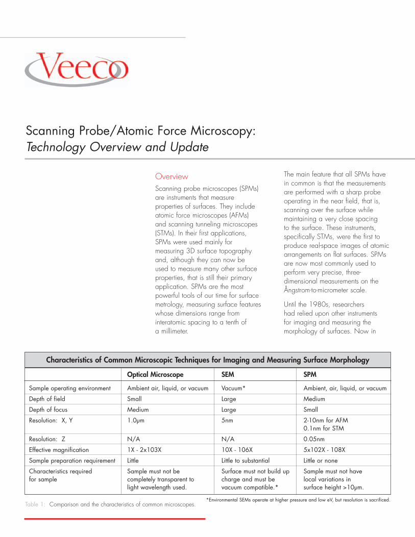
Figure 8. Condensed deoxyribonucleic acid(DNA) has been proposed as a gene deliverymechanism for biotechnology applications.Here, unfixed molecules were imaged in saltsolution. 20µm scan.
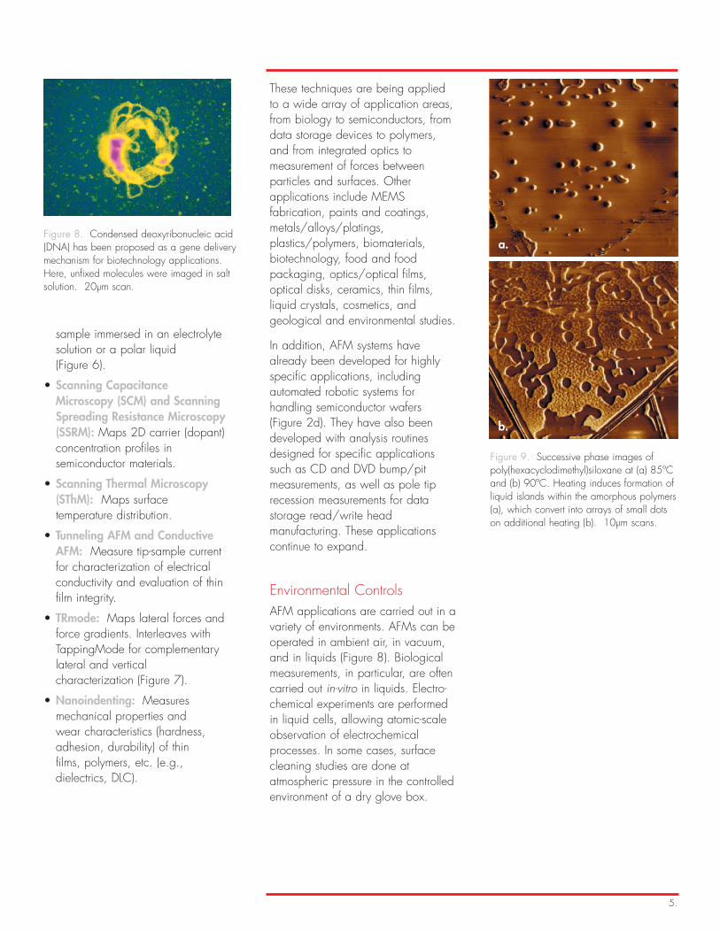
Figure 9. Successive phase images ofpoly(hexacyclodimethyl)siloxane at (a) 85ºCand (b) 90ºC. Heating induces formation ofliquid islands within the amorphous polymers(a), which convert into arrays of small dots on additional heating (b). 10µm scans.
a.
b.
5.

Figure 11a. AFM in-planenanomanipulation uses the AFM probe to image, manipulate nanometer-scaleobjects (carbon nanotubes), and imageagain to see the results.
Recent new products include heatingsystems for biological and polymerapplications up to 250°C (Figure 9),complete with sophisticated sampleand environmental sensing. Systemsare also now available for controllingthe gaseous environment of the sampleunder study (Figures 10a and b).
Recent Technology AdvancesNew hardware and software haveextended the utility of high-end SPMsystems beyond measurement andcharacterization to include nano-manipulation and nanolithography.Examples of in-plane and out-of-planenanomanipulation are shown in Figures 11a and 11b. An example of point-and-click nanolithography isseen in Figure 11c.
New controllers and electronics (e.g., the NanoScope IV and IVa SPM controllers) have been designed
Figure 11b. AFM out-of-planenanomanipulation uses the AFM probeto image, pull a single biomolecule out of the plane of the sample whilemeasuring the unfolding of themolecule, and image again to see theresults (in this case, the removal of onemolecule from an array).
Figure 11c. AFM nanolithography.
Figure 10a. (a.) TheAtmospheric Hood for theMultiMode SPM allows control ofthe gaseous imaging environmentto vary humidity or image underinert gases.
Figure 10b. The EnviroScope offers highvacuum, heating, electrochemical cell potentialcontrol, and purged gas environment.
6.

Figure 13. TappingMode+ height imageand zoom of a copolymer. The squareimage is a zoom into the boxed area in theoriginal rectangular image. This detail isrevealed by simply zooming in with softwareand without the need for time-consuming,repetitive smaller scans. Without this higherresolution scanning, the zoomed imagewould not have the pixel resolution requiredto view nanoscale details. 10µm x 1.24µmscan and 1µm x 1µm zoom.
to enhance performance relative to traditional designs. Some of the recent developments in AFMtechnology include:
Combined Environmental ControlsThe latest generation of SPMs offercombinations of environmentalcontrols, including vacuum and hightemperature (Figure 12).
Higher lateral resolutionAFM systems now provide higher data density to allow zooming into the finest details, even on large scans.This provides the resolution required to characterize sidewalls on suchsamples as DVD bumps/pits andsemiconductors. It also allowsobservation and measurement ofnanoscale details on large scans —without the need to spend additionaltime re-scanning the sample with asmaller scan area (Figure 13).
“Q“– controlControlling the quality factor, or Q, of the oscillating AFM probe allowsbetter control of the forces between tip and sample and improves thesensitivity of measurements such as with PhaseImaging and MFM(Figure 14).
Figure 12. Poly-sbs at room temperature inair (a) and at 180°C in 10-5 Torr pressure(b). Images captured with the Enviroscope(Figure 10b).
Figure 14. Images of the same area on magnetic recording tapescanned with and without Q-control. Phase detection MFM images andaverage cross-section measurements of the probe phase shift illustratenearly 4x enhanced signal-to-noise ratio for the Q-controlled image.15µm scans.
7.
a.
b.

Solutions for a nanoscale world.™
Veeco Instruments Inc.112 Robin Hill Road
Santa Barbara, CA 93117Find out more at www.veeco.com
805-967-1400 · 1-888-24-VEECO
AN48, Rev A2
© 2005 Veeco Instruments Inc. All rights reserved.
MultiMode, Dimension, LiftMode, and PhaseImaging are trademarks of Veeco Instruments Inc.
NanoScope is a registered trademark of Veeco Instruments Inc.
New scanning and measurementtechnologies have expanded therange of measurements and thusfurther increased the utility of AFM for a broad variety of applications.These developments have taken AFM, in a few short years, from a laboratory curiosity to one of the most powerful, flexible, andwidely used technologies for surface characterization.
Readers of this article are welcome to learn more about AFM technologyand applications by visitingwww.veeco.com. Application noteson most of the scanning technologiespresented here are available on the website or in hard copy upon request.
SummaryScanning tunneling microscopyproduced dramatic images of atomiclattices and atomic force microscopybroadened the technology to non-conductive surfaces. Developmentof atomic force microscopes hasallowed scientists and engineers tosee structure and detail withunprecedented resolution and withoutthe need for rigorous samplepreparation. Several advances havefurther extended this technique’s utilityto a wide range of applications.TappingMode permits imaging of softmaterials without damage to thesample and LiftMode allows separatebut simultaneous imaging oftopography and other parameters,such as magnetic or electric forces,without cross-contamination.PhaseImaging has opened up thecapability for mapping of surfacecompositional variations.