Embed Size (px)
Citation preview
Scanning Probe Microscopy Study of Molecular Self Assembly Behavior on Graphene Two-
dimensional Material
Yanlong Li
Dissertation submitted to the faculty of the Virginia Polytechnic Institute and State University in
partial fulfillment of the requirements for the degree of
Doctor of Philosophy
In
Physics
James R. Heflin, Chair
Chenggang Tao
Hans Robinson
Shengfeng Cheng
December 9, 2019
Blacksburg, VA
Keywords: Scanning Tunneling Microscope (STM), Molecular Self Assembly, Atomic Force
Microscope (AFM), Graphene, 2D materials
Copyright 2019
Scanning Probe Microscopy Study of Molecular Self Assembly Behavior on Graphene Two-
dimensional material
Yanlong Li
Academic Abstract
Graphene, one-atom-thick planar sheet of carbon atoms densely packed in a honeycomb
crystal lattice, has grabbed appreciable attention due to its exceptional electronic, mechanical
and optical properties. Chemical functionalization schemes are needed to integrate graphene
with the different materials required for potential applications. Molecular self-assembly
behavior on graphene is a key method to investigate the mechanism of interaction between
molecules and graphene and the promising applications related to molecular devices. In this
thesis, we report the molecular self-assembly behavior of phenyl-C61-butyric acid methyl ester
(PCBM), C60, perylenetetracarboxylic dianhydride (PTCDA) and Gd3N@C80 on flat and rippled
graphene 2D material by the experimental methods of scanning tunneling microscope (STM)
and atomic force microscope (AFM) and by the theoretical method of density functional theory
(DFT). We found that molecules form ordered structures on flat graphene, while they form
disordered structure on rippled graphene. For example, PCBM forms bilayer and monolayer
structures, C60 and Gd3N@C80 form hexagonal close packed (hcp) structure on flat graphene and
PTCDA forms herringbone structure on flat graphene surface. Although C60 and Gd3N@C80 both
form hcp structure, C60 forms a highly ordered hcp structure over large areas with little defects
and Gd3N@C80 forms hcp structure only over small areas with many defects. These differences
of structure that forms on flat graphene is mainly due to the molecule-molecule interactions
and the shape of the molecules. We find that the spherical C60 molecules form a quasi-
hexagonal close packed (hcp) structure, while the planar PTCDA molecules form a disordered
herringbone structure. From DFT calculations, we found that molecules are more effected by
the morphology of rippled graphene than the molecule-molecule interaction, while the
molecule-molecule interaction plays a main role during the formation process on flat graphene.
The results of this study clearly illustrate significant differences in C60 and PTCDA molecular
packing on rippled graphene surfaces.
Scanning Probe Microscopy Study of Molecular Self Assembly Behavior on Graphene Two-
dimensional material
Yanlong Li
General Audience Abstract
As the first physical isolated two-dimensional (2D) material, graphene has attracted exceptional
scientific attention. Due to its impressive properties including high carrier density, flexibility and
transparency, graphene has numerous potential applications, such as solar cell, sensors and
electronics. 2D molecular self-assembly is an area that focuses on organization and interaction
between self-assembly behaviors of molecules on surface. Graphene is an excellent substrate
for the study of molecular self-assembly behavior, and study of molecular study is very
important for graphene due to potential applications of molecules on graphene. In this thesis,
we present investigations of the molecular self-assembly of PCBM, C60, PTCDA and Gd3N@C80
on graphene substrate.
First, we report the two types of bilayer PCBM configuration on HOPG with a step height of 1.68
nm and 1.23 nm, as well as two types of monolayer PCBM configuration with a step height of
0.7 nm and 0.88 nm, respectively. On graphene, PCBM forms one type of PCBM bilayer with a
step height of 1.37 nm and one type of PCBM monolayer with a step height of 0.87 nm. By
building and analyzing the models of PCBM bilayers and monolayers, we believe the main
differences between two configurations of PCBM bilayer and monolayer is the tilt angle
between PCBM and HOPG, which makes type I configuration the higher molecule density and
binding energy.
Secondly, we report the investigation of self-assembly behaviors of C60 and PTCDA on flat
graphene and rippled graphene by experimental scanning tunneling microscope (STM) and
theoretical density functional theory (DFT). On flat graphene, C60 forms hexagon close pack
(hcp) structure, while PTCDA forms herringbone structure. On rippled graphene, C60 forms
quasi-hcp structure while PTCDA forms disordered herringbone structure. By DFT calculation,
we study the effect of graphene curvature on spherical C60 and planar PTCDA.
Finally, we report a STM study of a monolayer of Gd3N@C80 on graphene substrate. Gd3N@C80
forms hcp structure in a small domain with a step height of 0.88 nm and lattice constant of 1.15
nm. According to our DFT calculation, for the optimal organization of Gd3N@C80 and graphene,
the gap between Gd3N@C80 and graphene is 3.3 Å and the binding energy is 0.95 eV. Besides,
the distance between Gd3N@C80 and Gd3N@C80 is 3.5 Å and the binding energy is 0.32 eV.

VI
This thesis is dedicated
To my parents Bingyan Li (李炳炎) and Hanying Zhou (周含英)
To my sister Hui Li (李蕙)
To my girlfriend Chen Song (宋晨)
VII
Acknowledgements
I would express gratitude to my research advisor, Professor James R. Heflin, for the academic
guidance and support during my PhD career. He has been my role model as a scientific
researcher. He always encouraged me to work independently and bravely different idea of
experiments. He also gave me rigorous training on experiment and knowledge in physics.
Besides, he provide many opportunities for me to work in different fields and cooperate with
different groups. Overall, he taught me how to be a good physical experimenter.
I am grateful to many faculty members in Virginia Tech, especially my committee members.
Firstly, I would like to thank Professor Chenggang Tao for guiding my research in STM field.
Professor Shengfeng Cheng, as one of my committee members, taught me to learn physics
more intuitively, without heavily depending on mathematics. Professor Hans Robinson gave me
good suggestions on scientific presentation. Professor Greg Liu help in the field of metasurface
and Ag-nanoprism.
A huge thank to Dr. Chuanhui Chen from Professor Tao group for teaching me how to operate
STM, as well as numerous other helps during our collaboration. Besides, I particular want to
thank Dr. Xiaoyang Liu from Professor Dorn group, who did the most DFT calculation in this
thesis. I also need to thank Dr. Moataz Khalifa, who trained me using AFM, and Dr. Jonathan
Metzman showing me the preparation of organic molecules solution.
VIII
Table of Contents Table of Contents ......................................................................................................................... VIII
List of Figures ............................................................................................................................... XIII
Chapter 1: Introduction .................................................................................................................. 1
1.1 2D Materials .............................................................................................................................. 2
1.1.1 Graphene .............................................................................................................................. 2
1.1.2 Other 2D Materials ................................................................................................................ 3
1.2 Molecular Self-assembly ........................................................................................................... 4
1.2.1 Two-Dimensional Self-assembly ........................................................................................... 5
1.2.2 DNA Self-assembly ................................................................................................................ 5
1.2.3 Macromolecular Assembly ................................................................................................... 6
1.2.4 Self-assembly Monolayers (SAMs) ........................................................................................ 7
1.3 Molecular Self-assembly on Graphene ..................................................................................... 8
1.4 Document Organization ........................................................................................................... 8
References .................................................................................................................................... 11
Chapter 2: Literature Review ...................................................................................................... 14
2.1 Introduction and Background ................................................................................................ 14
2.2 Graphene ................................................................................................................................ 15
IX
2.2.1 Synthesis Methods of Graphene ......................................................................................... 16
2.2.1.1 Exfoliation and Cleavage .................................................................................................. 17
2.2.1.2 Epitaxy .............................................................................................................................. 20
2.2.1.3 Chemical Vapor Deposition .............................................................................................. 22
2.2.2 Properties of Graphene ...................................................................................................... 24
2.2.2.1 Single Layer: Tight-binding Theory .................................................................................. 25
2.2.2.2 Single Layer: Properties ................................................................................................... 27
2.2.2.3 Bilayer and Trilayer Graphene ......................................................................................... 31
2.2.3 Applications of Graphene ................................................................................................... 34
2.2.3.1 Graphene Field Emission (FE) .......................................................................................... 34
2.2.3.2 Graphene Field Effect Transistors (FET) ........................................................................... 35
2.2.3.3 Graphene-based Gas and Biological Sensors .................................................................... 37
2.2.3.4 Transparent Electrode ...................................................................................................... 38
2.2.3.5 Batteries ............................................................................................................................ 40
2.3 2D Molecular Self-assembly.................................................................................................... 41
2.3.1 Metal Bonds Molecular Self-assembly ................................................................................ 43
2.3.2 Hydrogen Bonding Molecular Self-assembly ...................................................................... 45
2.3.3 Van der Waals Molecular Self-assembly ............................................................................. 47
2.3.4 Halogen‐halogen Molecular Self-assembly ........................................................................ 49
X
2.4 Molecular Self-assembly on Graphene .................................................................................. 51
2.4.1 PTCDA .................................................................................................................................. 52
2.4.2 C60 ...................................................................................................................................... 55
2.4.3 Phthalocyanines .................................................................................................................. 57
References .................................................................................................................................... 60
Chapter 3: Experimental Methods .............................................................................................. 65
3.1 Introduction to Atomic Force Microscope (AFM) ................................................................... 66
3.1.1 Working Principle: Van der Waals Force ............................................................................. 68
3.1.2 Working Modes .................................................................................................................... 71
3.1.3 Bruker Dimension Icon® AFM .............................................................................................. 75
3.1.4 The Correction of Height of AFM Measurement ................................................................. 77
3.2 Introduction to Scanning Tunneling Microscope (STM) ......................................................... 78
3.2.1 Working Principle: Tunneling Effect .................................................................................... 80
3.2.2 Working Modes .................................................................................................................... 83
3.2.3 Omicron RT® STM ................................................................................................................ 85
3.2.4 The Correction of Height of STM Measurement ................................................................. 88
3.3 Sample Preparation ................................................................................................................ 88
3.3.1 Spin Coating ......................................................................................................................... 88
XI
3.3.2 Physical Vapor Deposition ................................................................................................... 89
References .................................................................................................................................... 90
Chapter 4: Self-Assembled PCBM Bilayers on Graphene and HOPG Examined by AFM and STM
....................................................................................................................................................... 94
4.1 Introduction ............................................................................................................................ 94
4.2 Experimental Methods ........................................................................................................... 96
4.3 Results and Discussion ............................................................................................................ 97
4.3.1 PCBM Bilayer Morphology ................................................................................................... 97
4.3.2 PCBM Monolayer Morphology .......................................................................................... 100
4.3.3 Discussion........................................................................................................................... 103
4.3.4 Thermal Effects .................................................................................................................. 109
4.4 Conclusion ............................................................................................................................. 110
References .................................................................................................................................. 111
Chapter 5: Differences in Self-Assembly of Spherical C60 and Planar PTCDA on Rippled
Graphene Surfaces .................................................................................................................... 114
5.1 Introduction .......................................................................................................................... 114
5.2 Experimental and Computational Methods ......................................................................... 116
5.3 Discussions ............................................................................................................................ 117

XII
5.4 Conclusion ............................................................................................................................. 130
References .................................................................................................................................. 132
Chapter 6: Self-Assembled Gd3N@C80 Monolayer on Graphene Examined by STM ............... 135
6.1 Introduction and Background ............................................................................................... 135
6.2 Experimental and Computational Methods ......................................................................... 139
6.3 Results and Discussions ........................................................................................................ 140
6.4 Conclusion ............................................................................................................................. 149
References .................................................................................................................................. 149
Chapter 7: Conclusion and Future Work ................................................................................... 152
7.1 The Bilayer PCBM Structure Formed on Graphene and HOPG ........................................... 152
7.2 The Ordered of C60 and Disordered Structure of PTCDA Formed on Rippled Graphene ..... 153
7.3 The hcp Structure of Gd3N@C80 Formed on Graphene ........................................................ 154
7.4 Future Work .......................................................................................................................... 155
XIII
List of Figures
Chapter 2
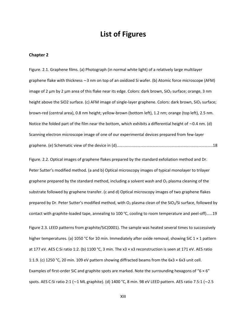
Figure. 2.1. Graphene films. (a) Photograph (in normal white light) of a relatively large multilayer
graphene flake with thickness ∼3 nm on top of an oxidized Si wafer. (b) Atomic force microscope (AFM)
image of 2 μm by 2 μm area of this flake near its edge. Colors: dark brown, SiO2 surface; orange, 3 nm
height above the SiO2 surface. (c) AFM image of single-layer graphene. Colors: dark brown, SiO2 surface;
brown-red (central area), 0.8 nm height; yellow-brown (bottom left), 1.2 nm; orange (top left), 2.5 nm.
Notice the folded part of the film near the bottom, which exhibits a differential height of ∼0.4 nm. (d)
Scanning electron microscope image of one of our experimental devices prepared from few-layer
graphene. (e) Schematic view of the device in (d)……..…………………………………………………………………………..18
Figure. 2.2. Optical images of graphene flakes prepared by the standard exfoliation method and Dr.
Peter Sutter’s modified method. (a and b) Optical microscopy images of typical monolayer to trilayer
graphene prepared by the standard method, including a solvent wash and O2 plasma cleaning of the
substrate followed by graphene transfer. (c and d) Optical microscopy images of two graphene flakes
prepared by Dr. Peter Sutter’s modified method, with O2 plasma clean of the SiO2/Si surface, followed by
contact with graphite-loaded tape, annealing to 100 oC, cooling to room temperature and peel-off)……19
Figure 2.3. LEED patterns from graphite/SiC(0001). The sample was heated several times to successively
higher temperatures. (a) 1050 °C for 10 min. Immediately after oxide removal, showing SiC 1 × 1 pattern
at 177 eV. AES C:Si ratio 1:2. (b) 1100 °C, 3 min. The x3 × x3 reconstruction is seen at 171 eV. AES ratio
1:1.9. (c) 1250 °C, 20 min. 109 eV pattern showing diffracted beams from the 6x3 × 6x3 unit cell.
Examples of first-order SiC and graphite spots are marked. Note the surrounding hexagons of “6 × 6”
spots. AES C:Si ratio 2:1 (∼1 ML graphite). (d) 1400 °C, 8 min. 98 eV LEED pattern. AES ratio 7.5:1 (∼2.5
XIV
ML graphite). (e) STM image of a surface region of the sample described in Figure 1d. Inset: Atomically
resolved region (different sample, similar preparation). (f) UHV-SEM image of a large area of the
Ru(0001) surface after first-layer graphene growth. Inset: Carbon KLL (260.6 eV) UHV scanning Auger
microscopy image, obtained on this sample. (g) AFM image of as-grown graphene on h-BN, the scale bar
is 200 nm……………………………………………………………………………………………………………………………………………….21
Figure. 2.4. (a) SEM images of as-grown graphene films on thin (300-nm) nickel layers and thick (1-mm)
Ni foils (inset). (b) TEM images of graphene films of different thicknesses. (c) Optical image of the grown
graphene transferred from the Ni surface in panel a to another SiO2/Si substrate. (d-e) High-
magnification TEM images showing the edges of film regions consisting of one (d) and three (e)
graphene layers. The cross-sectional view is enabled by the folding of the film edge. The in-plane lattice
fringes suggest local stacking order of the graphene layers.………………………………………………………………..23
Figure. 2.5. (a) Honeycomb lattice and its Brillouin zone. Left: lattice structure of graphene, made from
two interpenetrating triangular lattices (a1 and a2 are the lattice unit vectors, and δ𝑖, i= 1, 2, 3 are the
nearest-neighbor vectors). Right: corresponding Brillouin zone. The Dirac cones are located at the K and
K′ points.37 (b) Electronic dispersion in the honeycomb lattice. Left: energy spectrum (in units of t) for
finite values of t and t′, with t= 2.7 eV and t′=−0.2t. Right: zoom in of the energy bands close to one of
the Dirac points……………………………………………………………………………………………………………………………………..26
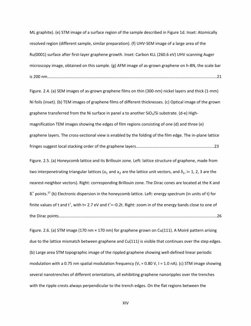
Figure. 2.6. (a) STM image (170 nm × 170 nm) for graphene grown on Cu(111). A Moire pattern arising
due to the lattice mismatch between graphene and Cu(111) is visible that continues over the step edges.
(b) Large area STM topographic image of the rippled graphene showing well-defined linear periodic
modulation with a 0.75 nm spatial modulation frequency (Vs = 0.80 V, I = 1.0 nA). (c) STM image showing
several nanotrenches of different orientations, all exhibiting graphene nanoripples over the trenches
with the ripple crests always perpendicular to the trench edges. On the flat regions between the
XV
trenches, a Moiré pattern can be observed. (d) Atomic-resolution STM image of a nanotrench exhibiting
subnanometer graphene ripples. The magnified insets exhibit the honeycomb graphene lattice both
over the flat substrate (bottom right) and the rippled region over the trenches (top left)……….……………28
Figure 2.7. (a) Scanning electron microscopy (SEM) image of a graphene flake spanning an array of
circular holes (scale bar, 3μm). (b) Schematic illustration of nanoindentation on membranes. (c)
Photograph of a 50‐μm aperture partially covered by graphene and its bilayer. The line scan profile
shows the intensity of transmitted white light along the yellow line. Inset shows the sample design: a 20
μm thick metal support structure has apertures 20, 30, and 50 μm in diameter with graphene flakes
deposited over them. (d) Optical image of graphene flakes with one, two, three, and four layers on a
285‐nm thick SiO2‐on‐Si substrate………………………………………………………………………………………………………….30
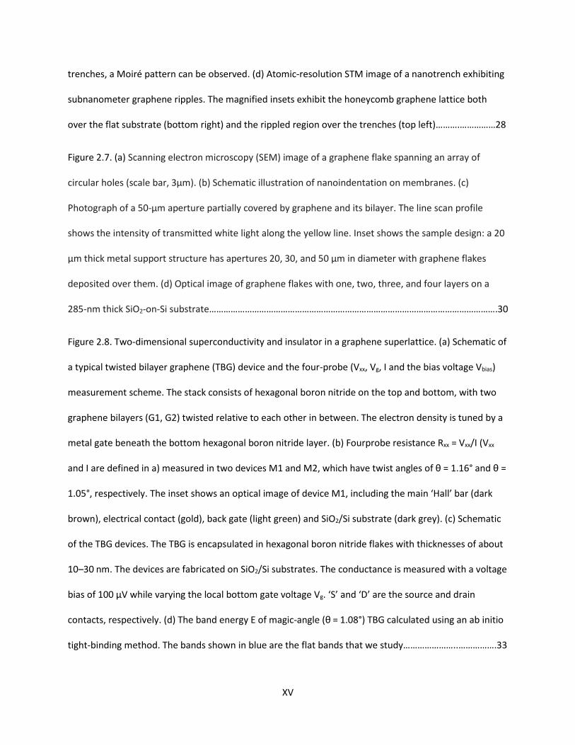
Figure 2.8. Two-dimensional superconductivity and insulator in a graphene superlattice. (a) Schematic of
a typical twisted bilayer graphene (TBG) device and the four-probe (Vxx, Vg, I and the bias voltage Vbias)
measurement scheme. The stack consists of hexagonal boron nitride on the top and bottom, with two
graphene bilayers (G1, G2) twisted relative to each other in between. The electron density is tuned by a
metal gate beneath the bottom hexagonal boron nitride layer. (b) Fourprobe resistance Rxx = Vxx/I (Vxx
and I are defined in a) measured in two devices M1 and M2, which have twist angles of θ = 1.16° and θ =
1.05°, respectively. The inset shows an optical image of device M1, including the main ‘Hall’ bar (dark
brown), electrical contact (gold), back gate (light green) and SiO2/Si substrate (dark grey). (c) Schematic
of the TBG devices. The TBG is encapsulated in hexagonal boron nitride flakes with thicknesses of about
10–30 nm. The devices are fabricated on SiO2/Si substrates. The conductance is measured with a voltage
bias of 100 μV while varying the local bottom gate voltage Vg. ‘S’ and ‘D’ are the source and drain
contacts, respectively. (d) The band energy E of magic-angle (θ = 1.08°) TBG calculated using an ab initio
tight-binding method. The bands shown in blue are the flat bands that we study…………………..…………….33
XVI
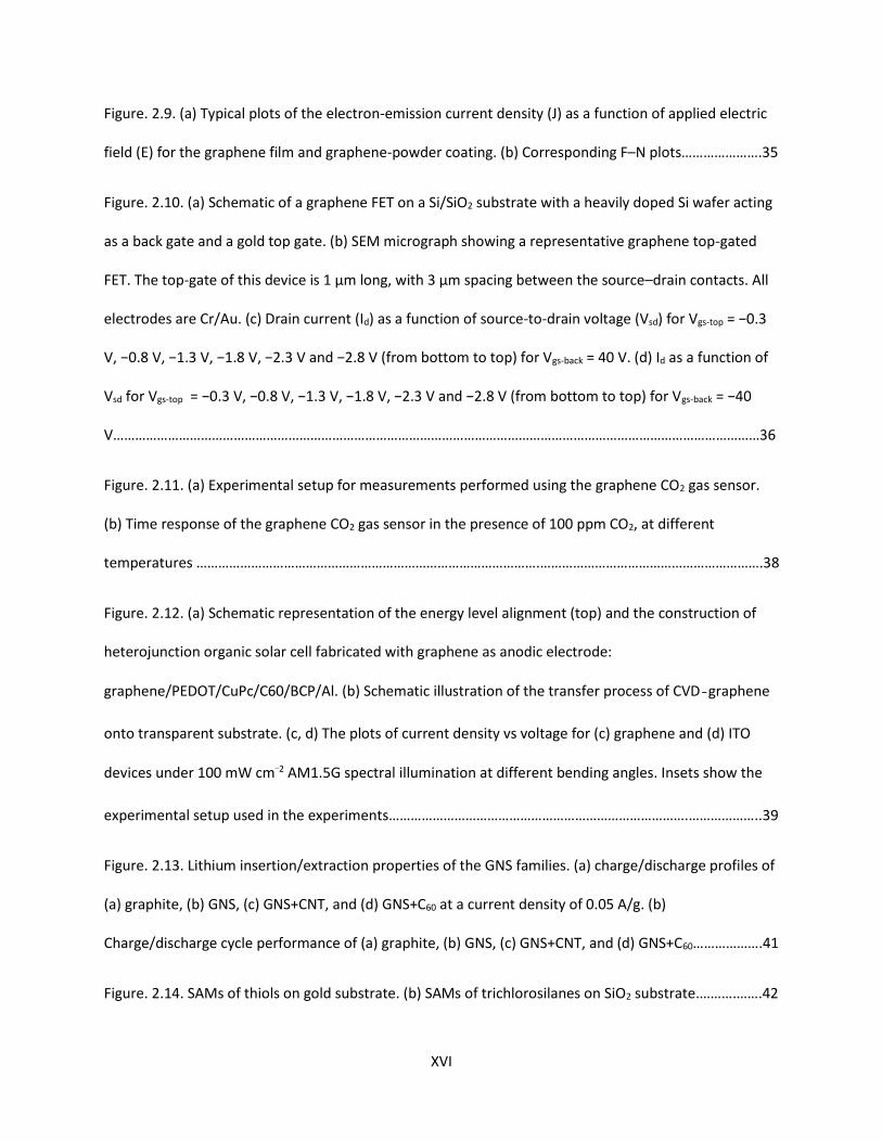
Figure. 2.9. (a) Typical plots of the electron-emission current density (J) as a function of applied electric
field (E) for the graphene film and graphene-powder coating. (b) Corresponding F–N plots………………….35
Figure. 2.10. (a) Schematic of a graphene FET on a Si/SiO2 substrate with a heavily doped Si wafer acting
as a back gate and a gold top gate. (b) SEM micrograph showing a representative graphene top-gated
FET. The top-gate of this device is 1 µm long, with 3 µm spacing between the source–drain contacts. All
electrodes are Cr/Au. (c) Drain current (Id) as a function of source-to-drain voltage (Vsd) for Vgs-top = −0.3
V, −0.8 V, −1.3 V, −1.8 V, −2.3 V and −2.8 V (from bottom to top) for Vgs-back = 40 V. (d) Id as a function of
Vsd for Vgs-top = −0.3 V, −0.8 V, −1.3 V, −1.8 V, −2.3 V and −2.8 V (from bottom to top) for Vgs-back = −40
V……………………………………………………………………………………………………………………………………………………………36
Figure. 2.11. (a) Experimental setup for measurements performed using the graphene CO2 gas sensor.
(b) Time response of the graphene CO2 gas sensor in the presence of 100 ppm CO2, at different
temperatures ………………………………………………………………………………….…………………………………………………….38
Figure. 2.12. (a) Schematic representation of the energy level alignment (top) and the construction of
heterojunction organic solar cell fabricated with graphene as anodic electrode:
graphene/PEDOT/CuPc/C60/BCP/Al. (b) Schematic illustration of the transfer process of CVD‐graphene
onto transparent substrate. (c, d) The plots of current density vs voltage for (c) graphene and (d) ITO
devices under 100 mW cm–2 AM1.5G spectral illumination at different bending angles. Insets show the
experimental setup used in the experiments……………………………………………………………………….………………..39
Figure. 2.13. Lithium insertion/extraction properties of the GNS families. (a) charge/discharge profiles of
(a) graphite, (b) GNS, (c) GNS+CNT, and (d) GNS+C60 at a current density of 0.05 A/g. (b)
Charge/discharge cycle performance of (a) graphite, (b) GNS, (c) GNS+CNT, and (d) GNS+C60……………….41
Figure. 2.14. SAMs of thiols on gold substrate. (b) SAMs of trichlorosilanes on SiO2 substrate.……….…….42
XVII
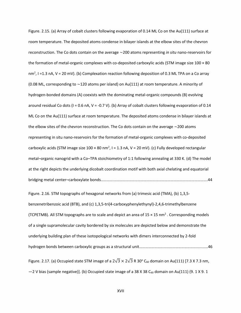
Figure. 2.15. (a) Array of cobalt clusters following evaporation of 0.14 ML Co on the Au(111) surface at
room temperature. The deposited atoms condense in bilayer islands at the elbow sites of the chevron
reconstruction. The Co dots contain on the average ∼200 atoms representing in situ nano-reservoirs for
the formation of metal-organic complexes with co-deposited carboxylic acids (STM image size 100 × 80
nm2, I =1.3 nA, V = 20 mV). (b) Complexation reaction following deposition of 0.3 ML TPA on a Co array
(0.08 ML, corresponding to ∼120 atoms per island) on Au(111) at room temperature. A minority of
hydrogen-bonded domains (A) coexists with the dominating metal-organic compounds (B) evolving
around residual Co dots (I = 0.6 nA, V = -0.7 V). (b) Array of cobalt clusters following evaporation of 0.14
ML Co on the Au(111) surface at room temperature. The deposited atoms condense in bilayer islands at
the elbow sites of the chevron reconstruction. The Co dots contain on the average ∼200 atoms
representing in situ nano-reservoirs for the formation of metal-organic complexes with co-deposited
carboxylic acids (STM image size 100 × 80 nm2, I = 1.3 nA, V = 20 mV). (c) Fully developed rectangular
metal–organic nanogrid with a Co–TPA stoichiometry of 1:1 following annealing at 330 K. (d) The model
at the right depicts the underlying dicobalt coordination motif with both axial chelating and equatorial
bridging metal center–carboxylate bonds………….………………………………………………………………………………….44
Figure. 2.16. STM topographs of hexagonal networks from (a) trimesic acid (TMA), (b) 1,3,5-
benzenetribenzoic acid (BTB), and (c) 1,3,5-tri(4-carboxyphenylethynyl)-2,4,6-trimethylbenzene
(TCPETMB). All STM topographs are to scale and depict an area of 15 × 15 nm2 . Corresponding models
of a single supramolecular cavity bordered by six molecules are depicted below and demonstrate the
underlying building plan of these isotopological networks with dimers interconnected by 2-fold
hydrogen bonds between carboxylic groups as a structural unit……………………………………………………………46
Figure. 2.17. (a) Occupied state STM image of a 2√3 × 2√3 R 30o C60 domain on Au(111) [7.3 X 7.3 nm,
—2 V bias (sample negative)]. (b) Occupied state image of a 38 X 38 C60 domain on Au(111) (9. 1 X 9. 1
XVIII
nm, —2 V). (c) Filled states (VSB = −1.5V) and (b) empty states STM image (VSB = 1.5V) of close-packed
Sc3N@C80 on Au(111)/mica (It = 0.08 nA). The circled molecules appear bright in filled states and dark in
empty states. Vacancies always show as black holes……………………………………………………………………………..48
Figure. 2.18. The two ordered self-assembly phases of HPBI on Au(111). (a) The chemical structure of
HPBI. Carbon, grey; iodine, red; hydrogen, white. (b) Large-scale STM image of the coexisting α and β
phases. The crystalline axes of the Au substrate are labelled. (c, d) STM images of the pure α (c) and β (d)
phase domains. The white arrows in c designate the herringbone structure in the α phase; the α and β
phase unit cells are represented by red and blue rhombi, respectively. (e, f) Magnified STM images of
the α (e) and β (f) phases. HPBI molecules are labelled by the dashed white and green circles. The
dashed white triangle in e highlights the I–I trimer. The solid yellow circles in f highlight the
adatoms………………………………………………………………………………………………………………………………………………..50
Figure. 2.19. The molecular structure of (a) Phthalocyanine, (b) C60 and (c) PTCDA……………………………….52
Figure. 2.20. (a) PTCDA monolayer on bilayer graphene at T=4.7 K. The shadow-like structure
originates from the SiC interface layer below bilayer graphene. UT=1.5V, IT=3.8pA. (b) Close-up of (a) One
clearly recognizes the assembly of the PTCDA molecules. UT=1V, IT=3.8pA. (c) Monolayer coverage of
PTCDA on epitaxial graphene. (d) Molecular-resolution STM image of the PTCDA monolayer. The PTCDA
molecular structure and unit cell outline are overlaid. The monolayer continuously follows the graphene
sheet over the SiC step edge……………………………………………………………………………………………………….…………53
Figure. 2.21. (a) Calculated geometry configuration of monolayer PTCDA molecules on a
graphene/Pt(111). (b) Experimental STS spectra on one monolayer PTCDA on graphene/Pt(111). (c) Local
Density of States (LDOS) around the transport gap on PTCDA in the DFT calculations for the
PTCDA/graphene/Pt(111) system. Two peaks are clearly resolved both in the experimental and in the
XIX
theoretical spectra whose origin can be ascribed to the HOMO and LUMO of the PTCDA
molecule………………………………………………………………………….…………………………………………………………………….54
Figure. 2.22. (a) STM topographic images of the initial stages of growth of C60 molecules adsorbed on a
submonolayer of epitaxial graphene on SiC. (b) a close-up view of the blue box indicated in (a) displaying
the single vacancy of a C60 molecule and the domain boundary between molecular islands. Images (a and
b) were acquired with I = 20 pA and V = −2 V. (c) Large-area STM topography of substrate commensurate
growth of C60 molecules on G/Ru. Right part is a higher terrace of Ru(0001) surface. (Vs = 3.0 V and I =
0.05 nA) (d) Zoom-in image of the supramolecular structure. The unit cells of the underlying substrate
and molecular lattice are outlined by large and small rhombuses, respectively. (2.0 = V and 0.1 = nA). (e)
High resolution image of bimolecular and trimolecular C60 chains. Within the chains, the C60-C60
intermolecular spacing is ~1.0nm, and the interchain distance, defined as the distance between the
centers of adjacent C60 rows belonging to neighboring chains, is 1.23 nm (Vs= 1.95 V, I= 0.50nA). (f) A
line profile along the close packed orientation as marked with the dashed blue line in (e). (g) Scheme of
an individual C60 molecule preferentially trapped in the Chcp valley at RT and its corresponding STM
image as shown in (i). (h) Scheme of six C60 molecules attached to the trapped C60 as a seed for the
nucleation of monolayer C60 islands; C60-C60 cohesive energy increases. (j) RT freezing of the thermal
motions of C60 in the Chcp valleys once a C60 monolayer is formed. (k) All C60 molecules trapped in Chcp
valleys display a dumbbell shape, aligning along the <1120> directions. The bright lobes in the dumbbell-
shaped correspond to pentagons of the C60 cage at positive sample bias, which suggests C60 orients with
the 6:6 bond (the C-C bond between two carbon hexagons) facing upward, as shown in the right top of
(k)………………… ………………………………………………………………………………………………………………………………………56
Figure. 2.23. (a) High-resolution image (U = 0.1 V, I = 0.5 nA) of three distinct regions of graphene, top,
fcc, and hcp, marked by triangles and dashed and solid hexagons, respectively. (b) STM image (U = −2.0
V, I = 0.05 nA) revealing that molecules first adsorb at the fcc regions. (c) Sequences of STM images (U =
XX
−2.0 V, I = 0.05 nA) of FePc molecules with increasing coverage. (d) Details of the Kagome lattice of FePc.
A trihexagonal tiling is highlighted. The unit cell of the Kagome lattice is marked with blue lines. (e)
Structural model of the Kagome lattice showing molecular orientation disorder. (f) STM image of a close-
packed FePc molecular island in showing a square lattice (indicated by the dashed square). (g) STM
image of a close-packed CoPc molecular island in a showing a square lattice. (h) STM image of a close-
packed CuPc molecular island in a showing a square lattice. (i) STM image of a close-packed F16CoPc
molecular island showing a square lattice. (j) STM images of self-assembled ClAlPc molecular arrays of
the first layer on graphene. The ClAlPc arrays show continuous films across the Cu steps. Insets show the
magnified images (Vtip = 2.0 V, I = 75 pA). (k) The optimized configuration for the F16CuPc/graphene
[(3,4)×(4,3)] system. (l) Total DOS (thick black solid line) and projected DOS on the Pc molecule (blue
solid line), on graphene (thin black solid line), upon F16CuPc adsorption on graphene, and the DOS of the
isolated graphene (black dashed dotted line). The vertical dotted line shows the Fermi level.…..….………59
Chapter 3
Figure. 3.1. Schematic drawing shows the mechanism of imaging mode in AFM……………………………………67
Figure 3.2. Force – distance curve of a Van Der Waals force. The yellow part is the non-contact mode
region, the purple is the contact mode region and the green part is the intermittent contact (tapping)
mode region……………………………………………………………………………………………………………………………….…………70
Figure 3.3. (a) The schematic drawing of contact mode. (b) The schematic drawing of non-contact mode.
(c) The schematic drawing of tapping mode………………………………………………………………………………………….72
Figure 3.4. (a) Resonance curve of a Tapping Mode cantilever above the surface. (b) Resonance curve of
a Tapping Mode cantilever close to the surface. Note that the resonance shifts to lower frequencies and
exhibits a drop in amplitude………………………………………………………………………………………………………………….75
XXI
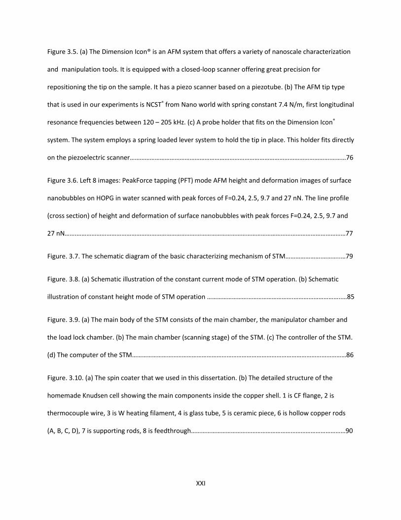
Figure 3.5. (a) The Dimension Icon® is an AFM system that offers a variety of nanoscale characterization
and manipulation tools. It is equipped with a closed-loop scanner offering great precision for
repositioning the tip on the sample. It has a piezo scanner based on a piezotube. (b) The AFM tip type
that is used in our experiments is NCST® from Nano world with spring constant 7.4 N/m, first longitudinal
resonance frequencies between 120 – 205 kHz. (c) A probe holder that fits on the Dimension Icon®
system. The system employs a spring loaded lever system to hold the tip in place. This holder fits directly
on the piezoelectric scanner………………………………………………………………………………………………………….………76
Figure 3.6. Left 8 images: PeakForce tapping (PFT) mode AFM height and deformation images of surface
nanobubbles on HOPG in water scanned with peak forces of F=0.24, 2.5, 9.7 and 27 nN. The line profile
(cross section) of height and deformation of surface nanobubbles with peak forces F=0.24, 2.5, 9.7 and
27 nN…….………………………………………………………………………………………………………………………………………………77
Figure. 3.7. The schematic diagram of the basic characterizing mechanism of STM………………….………..…79
Figure. 3.8. (a) Schematic illustration of the constant current mode of STM operation. (b) Schematic
illustration of constant height mode of STM operation …………………………………………….………………………..…85
Figure. 3.9. (a) The main body of the STM consists of the main chamber, the manipulator chamber and
the load lock chamber. (b) The main chamber (scanning stage) of the STM. (c) The controller of the STM.
(d) The computer of the STM…………………………………………………………………………………………………………………86
Figure. 3.10. (a) The spin coater that we used in this dissertation. (b) The detailed structure of the
homemade Knudsen cell showing the main components inside the copper shell. 1 is CF flange, 2 is
thermocouple wire, 3 is W heating filament, 4 is glass tube, 5 is ceramic piece, 6 is hollow copper rods
(A, B, C, D), 7 is supporting rods, 8 is feedthrough…………………………………………………………………………………90
XXII
Chapter 4
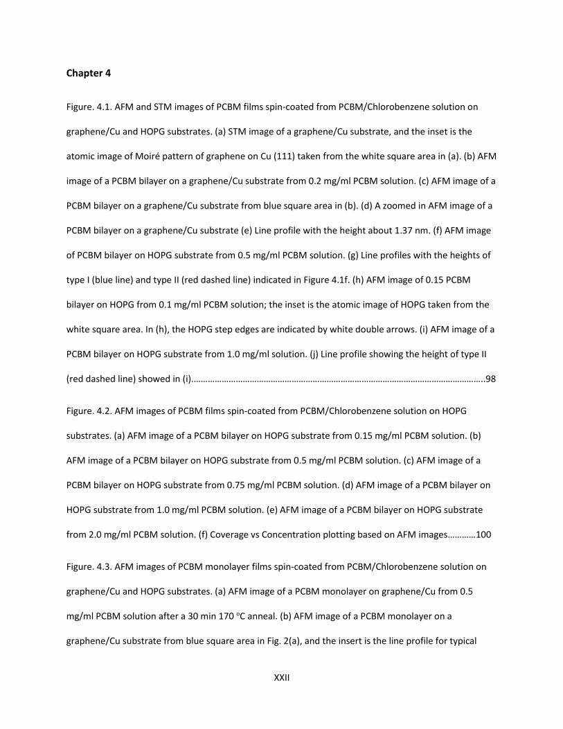
Figure. 4.1. AFM and STM images of PCBM films spin-coated from PCBM/Chlorobenzene solution on
graphene/Cu and HOPG substrates. (a) STM image of a graphene/Cu substrate, and the inset is the
atomic image of Moiré pattern of graphene on Cu (111) taken from the white square area in (a). (b) AFM
image of a PCBM bilayer on a graphene/Cu substrate from 0.2 mg/ml PCBM solution. (c) AFM image of a
PCBM bilayer on a graphene/Cu substrate from blue square area in (b). (d) A zoomed in AFM image of a
PCBM bilayer on a graphene/Cu substrate (e) Line profile with the height about 1.37 nm. (f) AFM image
of PCBM bilayer on HOPG substrate from 0.5 mg/ml PCBM solution. (g) Line profiles with the heights of
type I (blue line) and type II (red dashed line) indicated in Figure 4.1f. (h) AFM image of 0.15 PCBM
bilayer on HOPG from 0.1 mg/ml PCBM solution; the inset is the atomic image of HOPG taken from the
white square area. In (h), the HOPG step edges are indicated by white double arrows. (i) AFM image of a
PCBM bilayer on HOPG substrate from 1.0 mg/ml solution. (j) Line profile showing the height of type II
(red dashed line) showed in (i).……………………………………………………………………………………………………………..98
Figure. 4.2. AFM images of PCBM films spin-coated from PCBM/Chlorobenzene solution on HOPG
substrates. (a) AFM image of a PCBM bilayer on HOPG substrate from 0.15 mg/ml PCBM solution. (b)
AFM image of a PCBM bilayer on HOPG substrate from 0.5 mg/ml PCBM solution. (c) AFM image of a
PCBM bilayer on HOPG substrate from 0.75 mg/ml PCBM solution. (d) AFM image of a PCBM bilayer on
HOPG substrate from 1.0 mg/ml PCBM solution. (e) AFM image of a PCBM bilayer on HOPG substrate
from 2.0 mg/ml PCBM solution. (f) Coverage vs Concentration plotting based on AFM images…………100
Figure. 4.3. AFM images of PCBM monolayer films spin-coated from PCBM/Chlorobenzene solution on
graphene/Cu and HOPG substrates. (a) AFM image of a PCBM monolayer on graphene/Cu from 0.5
mg/ml PCBM solution after a 30 min 170 oC anneal. (b) AFM image of a PCBM monolayer on a
graphene/Cu substrate from blue square area in Fig. 2(a), and the insert is the line profile for typical
XXIII
PCBM monolayer with height of 0.87 nm. (c) AFM image of a PCBM monolayer on HOPG from 0.5 mg/ml
PCBM solution. (d) Line profile along the line marked in (c) indicates the height of 0.71 nm. (e) AFM
image of a PCBM monolayer on HOPG from 0.5 mg/ml solution. (f) Line profile along the line marked in
(e) shows the height is about 0.88 nm…………………………………………………………………………………………………102
Figure. 4.4. Two schematic model configurations of a PCBM monolayer on a graphene or HOPG
substrate: C atom in PCBM (blue), C atom in the substrate (green), O atom (red), and H atom (yellow).
(a) Top and side views of one model configuration of a PCBM monolayer with height of 0.9 nm (b) Top
and side views of another model configuration of a PCBM monolayer sample of with height of 0.7 nm.
The dashed parallelograms in (a) and (b) indicate unit cells……………………………………………………………….104
Figure. 4.5. Schematic diagrams of type I and type II configurations of a PCBM bilayer on a graphene or
HOPG substrate: C atom in PCBM (blue), C atom in the substrate (green), O atom (red), and H atom
(yellow). (a) Top and side views of type I configuration of the PCBM bilayer. In the side view, the dashed
tilted rectangle highlights a PCBM dimer cell, and the solid rectangle indicates the hydrogen binding
within a PCBM dimer, while the solid circle shows a side interaction between neighboring PCBM dimers.
(b) Top and side views of type II configuration of the PCBM bilayer. In the side view, the dashed tilted
rectangle highlights a PCBM dimer cell, while the solid rectangle indicates the hydrogen binding within a
PCBM dimer…………………………………………………………………………………………………………………………………………107
Figure. 4.6. AFM images of PCBM bilayer and size distributions of holes at different conditions. (a) AFM
image of a PCBM bilayer before annealing. (b) AFM image of a PCBM bilayer after annealing at 140 °C.
(c) AFM image of a PCBM bilayer after annealing at 160 °C. (d) Area distribution histogram of holes
(without PCBM area) obtained from measurements of the area of holes in AFM images of before (red
line) and after annealing at 140 °C (dark red line) and 160 °C (dark blue line)………………………………..……110
XXIV
Chapter 5
Figure 5.1. STM topographical images of planar graphene (labeled as I), 1D-rippled graphene (II) and 2D-
rippled graphene (III) on Cu. (a) Large area STM image of planar graphene (I) and 1D-rippled graphene
(II) showing the linear periodic modulation and the spatial modulation frequencies (Vs = -2.340 V, I =
0.110 nA). (b) High-resolution STM image of 1-D rippled graphene (Vs = -0.340 V, I = 1.900 nA). (c) STM
image of the 1-D rippled graphene, observed from the square region marked in (b), the schematic model
on top of the atomic image shows the ripples along zigzag direction (Vs = -0.280 V, I = 1.900 nA). (d) Line
profile perpendicular to the 1D-rippled graphene (marked as a blue line in (b)) showing the periodic
modulation. (e) STM image of graphene on two different Cu facets, planar graphene (I) and 2D-rippled
graphene (III) (Vs = -2.74 V, I = 0.045 nA). (f) High-resolution STM image of 2D-rippled graphene,
observed from the dashed square region marked in (e) (Vs = -2.600 V, I = 0.068 nA). (g) A schematic
model shows 1D-rippled graphene sheet. (h) Large area STM image of planar graphene (I) and 1D-
rippled graphene (II) (Vs = -1.850 V, I = 0.340 nA). (i) Atomic STM image showing the moiré pattern of
planar graphene, observed from the dashed squared region marked in (h) (Vs = -1.850 V, I = 0.450
nA)……………………………………………………………………………………………………………………………………………………….118
Figure 5.2. STM topography images of one single-twin rippled graphene. (a) STM topographic image of
continuous graphene forming twin wrinkles on Cu(111) (Vs = -1.06 V, I = 0.315 nA). (b) Zoomed-in image
of (a) (Vs = -0.600 V, I = 0.850 nA). (c) Line profile of the single-twin wrinkle of graphene, measured along
the blue line in b. (d)Further zoomed-in STM topographic image of single-twin wrinkle of graphene (Vs =
-0.560 V, I = 0.8750 nA). (e) Atomic STM image of one of the twin wrinkles in Figure (d) showing the
honeycomb structure of graphene (Vs = -0.560 V, I = 0.8750 nA). (f) Schematic model of one side of the
twin wrinkle……………………………………………………………….………………………………………………………………….…….120
XXV
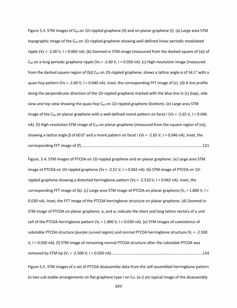
Figure 5.3. STM images of C60 on 1D-rippled graphene (II) and on planar graphene (I). (a) Large area STM
topographic image of the C60 on 1D-rippled graphene showing well-defined linear periodic modulated
ripple (Vs = -2.00 V, I = 0.060 nA). (b) Zoomed-in STM image (measured from the dashed square of (a)) of
C60 on a long periodic graphene ripple (Vs = -2.60 V, I = 0.050 nA). (c) High-resolution image (measured
from the dashed square region of (b)) C60 on 1D-rippled graphene, shows a lattice angle α of 54.1o with a
quasi-hcp pattern (Vs = -2.60 V, I = 0.040 nA). Inset, the corresponding FFT image of (c). (d) A line profile
along the perpendicular direction of the 1D-rippled graphene marked with the blue line in (c) (top), side
view and top view showing the quasi-hcp C60 on 1D-rippled graphene (bottom). (e) Large area STM
image of the C60 on planar graphene with a well-defined moiré pattern on facet I (Vs = -2.65 V, I = 0.046
nA). (f) High-resolution STM image of C60 on planar graphene (measured from the square region of (e)),
showing a lattice angle β of 60.0o and a moiré pattern on facet I (Vs = -2.65 V, I = 0.046 nA). Inset, the
corresponding FFT image of (f)…………………………………………………………………………………………………………….121
Figure. 5.4. STM images of PTCDA on 1D-rippled graphene and on planar graphene. (a) Large area STM
image of PTCDA on 1D-rippled graphene (Vs = -2.51 V, I = 0.042 nA). (b) STM image of PTCDA on 1D-
rippled graphene showing a distorted herringbone pattern (Vs = -2.510 V, I = 0.042 nA). Inset, the
corresponding FFT image of (b). (c) Large area STM image of PTCDA on planar graphene (Vs = 1.800 V, I =
0.030 nA). Inset, the FFT image of the PTCDA herringbone structure on planar graphene. (d) Zoomed-in
STM image of PTCDA on planar graphene; a1 and a2 indicate the short and long lattice vectors of a unit
cell of the PTCDA herringbone pattern (Vs = 1.800 V, I = 0.030 nA). (e) STM images of coexistence of
substable PTCDA structure (purple curved region) and normal PTCDA herringbone structure (Vs = -2.500
V, I = 0.030 nA). (f) STM image of remaining normal PTCDA structure after the substable PTCDA was
removed by STM tip (Vs = -2.500 V, I = 0.030 nA)…………………………………………………………..…………………….124
Figure 5.5. STM images of a set of PTCDA disassembly data from the self-assembled herringbone pattern
to two sub-stable arrangements on flat graphene type I on Cu. (a-i) are typical image of the disassembly
XXVI
process. All these images were obtained under the same scanning conditions: Vs = -2.500 V, I = 0.030 nA,
and with the same size of 23 nm × 23 nm. The purple curved frames in the images show the sub-stable
arrangement……………………………………………………………………………...……………………………………………………….125
Figure 5.6. Typical fullerene orientations on graphene. The computational results suggest that (b) is the
energetically favored orientation. Each grey sphere here is a carbon atom ………………………………………..127
Figure 5.7. Computational results for C60 on 1D-rippled graphene and planar graphene showing
energetically favored orientations. (a) C60 molecule on a peak site on curved-graphene, (b) C60 molecule
with a valley site on curved-graphene and (c) C60 on planar-graphene. (d) Plot of C60-graphene distance
versus relative energy for C60 on a graphene peak (pink), C60 in a graphene valley (blue) and C60 on planar
graphene (green)…………………………………………………………………………………………………………………………………128
Figure 5.8. DFT results for adsorbed molecule/graphene interactions. (a) Energy difference of a C60
molecule on a 1D-rippled graphene surface (b) Energy difference of a PTCDA molecule on a 1D-rippled
graphene. (c) Energy curve for a PTCDA molecule rotation on 1D-rippled graphene on a peak location
(top); favored PTCDA orientations (bottom). (d) Favored PTCDA orientations at the peak site (left) and at
the valley site (right)……………………………………………………………………………………………………………………………130
Chapter 6
Figure. 6.1. (a) STM image of C60 monolayer on graphene (Vs = 1.50 V, I = 0.050 nA). (b) The right image
is the line profile of monolayer C60 (yellow dashed line in figure 6.1a). The left image is the schematic
image of C60 on graphene with a gap about 0.3 nm, according to our DFT calculation. (c) STM image of
Gd3N@C80 monolayer on graphene (Vs = -1.84 V, I = 0.140 nA). (d) The right image is the line profile of
monolayer Gd3N@C80 (red dashed line in figure 6.1c). The left image is the schematic image of
Gd3N@C80 on graphene with a gap about 0.33 nm, according to our DFT calculation…….......................142
XXVII
Figure 6.2. STM images of Gd3N@C80 on graphene. (a) Large area STM topographic image of the
Gd3N@C80 on graphene showing two domains with different orientations and many defects (Vs = -1.84
V, I = 0.248 nA). (b) Zoomed-in STM image (measured from the dashed square of (a)) of Gd3N@C80 on a
graphene showing two domains with different orientations and one defect (Vs = -1.84 V, I = 0.248 nA).
(c) High-resolution image Gd3N@C80 on graphene (Vs = -1.84 V, I = 0.240 nA). (d) Zoomed-in STM image
(measured from the dashed square of (c)) of Gd3N@C80 on a graphene showing lattice constant of an
average about 1.15 nm (Vs = -1.84 V, I = 0.240 nA)……………………………………………………………………………..143
Figure. 6.3. (a) STM image of Gd3N@C80 on graphene after annealing at 200 oC (Vs = -1.69 V, I = 0.122
nA). (b) STM image of Gd3N@C80 on graphene after annealing at 250 oC (Vs = 1.50 V, I = 0.100 nA)…….144
Figure. 6.4. Typical Gd3N@C80 orientations on graphene. The computational results suggest that
orientation 3 is the energetically favored orientation…………………………………………….……………………………146
Figure. 6.5. Computational results for Gd3N@C80 on flat graphene of different orientations, showing
energetically favored orientation 3…….....................................................................................................147
Figure. 6.6. (a) DFT results for molecule-molecule interaction of different orientation between two
Gd3N@C80 molecules. (b) The two Gd3N@C80 molecules with two metal sides facing each other with an
angle between two Gd atoms facets. (c) The two Gd3N@C80 molecules with two metal atoms facing each
other with an angle between two Gd atoms facets…...............................................................................148
1
Chapter 1
Introduction
In December 1959, Richard Feynman delivered a famous speech ‘Plenty of Room at The
Bottom’. The possibility of direct manipulation of individual atoms, which Feynman described in
this lecture, could be a much more useful chemical synthetic method than those used at the
time.1 Lately, this speech is considered to be the beginning of the birth of nanotechnology,
although Roman glassmakers were fabricating glasses containing nanosized metal to obtain
certain unique colors. Nanotechnology is the combination of science, engineering, and
technology conducted at the nanoscale and involves nano-characterization techniques, nano-
materials, self-assembly and many related areas.
Nanoscale characterization techniques are the methods that we use to explore the nanoscale
world. As traditional microscopes do not function at the scale of nanometer due to diffraction
limitations, scientists and engineers have developed a set of instruments (STM, AFM, TEM, etc.)
to image and characterize nanoscale materials. Nanoscale material involves objects such as
nanoparticles and graphene. In addition, molecular self-assembly concerns the spontaneous
formation of a complex structure (with a defined arrangement) by small components such as
molecules or nanoparticles.
In this dissertation, we present a room temperature atomic resolution scanning tunneling
microscope (STM) investigation of the self-assembly behaviors of organic semiconductor
molecules on graphene substrate. Our collaborators have used the computational density
functional theory (DFT) approach to help us understand the interaction between molecules and
2
the interaction between a molecule and graphene better. Firstly, we deposit the molecules on
graphene to create the sample. Then we scan the morphology of the sample to investigate the
self-assembly behavior. Our collaborators then used the DFT calculations and compared the
results with our AFM or STM results to provide detailed physical interpretations.
1.1 2D Materials
Nanoscience is the field of science focus on the study of objects with at least one dimension at
the nanoscale, such as nanoparticles, nanofibers and two-dimensional (2D) materials. 2D
materials as usually named as an atomic layer of a crystalline material. Since the discovery of
graphene in 2004,2 2D materials have attracted extremely high attention. In the following
fifteen years, scientists found various families of 2D materials, including metals, semiconductors
and insulators.3
1.1.1 Graphene
Graphene, an atomic thin layered graphite, was the first true 2D material to be physically
demonstrated.2 It has attracted a lot of attention due to its unique electronic structure,
ultrahigh carrier mobility, thermal conductivity, and mechanical strength.4 The modification of
graphene, for specific electronic properties or functionalities, is required for next movement
towards real device fabrication of different potential applications .5 As graphene is an intrinsic
no bandgap semiconductor, its field of applications could be extended by creating a bandgap by
3
perturbations including controlled introduction of strain, confinement to nanoribbons, or
biasing of a bilayer graphene.6-8 Covalent or noncovalent chemical functionalization could
provide natively inert graphene chemically sensitive, which is crucial for the applications, and
allowing for electron accepting/donating organic molecules to perform charge‐transfer
doping/bandgap engineering.9-10 In a number of recent papers, the electronic effects
introduced by organic molecules on graphene have been discussed.11-13
On the other hand, graphene is also an appealing test substrate to investigate the properties
and mechanism of self-assembly behavior of molecules confined to two dimensions,14 due to
the fact that it could eliminate the effect of the substrate when compared to metal substrates.
Besides, 2D molecular self-assembly is a popular research area focus on understanding the
energetics of molecular organization with the purpose of building an anticipating method of
controlled synthesis of useful 2D structures.14 As a promising useful new material, new
opportunities may be brought by graphene to control and expand the applications of confined
2D molecular structures.14
1.1.2 Other 2D Materials.
In consideration of the success in the study of graphene, the methodology and ideas learned in
these studies have been applied to other layered materials.15 Therefore, in addition to the
current limited applicability of graphene, the field of 2D materials opens up new horizons for
new variety of possibilities. Fortunately, the idea of extracting a layer of strongly covalent in-
plane bonds and inter-layer weak van der Waals like coupling from three-dimensional materials
4
is not only applicable to graphite, but also fit to other layered materials.16 Examples of 2D
inorganic nanomaterials have blossomed during the last decades. Transition metal
dichalcogenides (TMDs),3 with the formula MX2 (where M is a transition metal and X is a
chalcogen), are the main categories of 2D materials and provide a wide range of electronic
properties, from metallic or semimetallic (V,17 Nb,18 and Ta19 dichalcogenides) to insulating or
semiconducting (Ti,20 Zr,21 Mo,22 and W23 dichalcogenides). Adding molecules to a TMDs’
surface is also a very good way to tune its properties. Besides, this also serves as a platform to
investigate the mechanics behind the interactions between molecule-molecule and molecule-
substrate.
1.2 Molecular Self-assembly
Molecular self-assembly is the process in which molecules are arranged in a determined
manner without applying external forces. There are two types of self-assembly, intermolecular
self-assembly24 and intramolecular self-assembly.25 Generally, and in this dissertation,
compared to the version of intramolecular which is more commonly called self-folding, the
term molecular self-assembly refers to intermolecular self-assembly. There are several kinds of
molecular self-assembly, including two-dimensional self-assembly,26 DNA nanotechnology,27
biology macromolecular assembly,28 self-assembly monolayers (SAMs)29 and so on.
5
1.2.1 Two-dimensional Self-assembly
The spontaneous monolayer molecular assembly at the surface is often referred to as two-
dimensional self-assembly. Non-surface active molecules can be assembled into ordered
structures by the intermolecular forces.30 Early direct proofs indicates that with the
development of scanning tunneling microscopy, non-surfactant molecules can be assembled
into higher-order structure at solid surface.31 Finally, two methods for the self-assembly of 2D
structure have become popular, namely self-assembly at the solid-liquid interface and self-
assembly after ultra-high-vacuum deposition and annealing.32 Self‐assembly of molecules at a
surface depends mainly on two kinds of interactions: non‐covalent molecule‐molecule
interaction defining the relationship between neighboring molecules, and molecule‐substrate
interaction stabilizing the molecules on the surface.14 Various different intermolecular
interactions can form 2D self‐assembly. Strong hydrogen bonds (such as carboxylic dimers33)
and strong directional bonds including coordination at metal centers34 can produce porous
assembly structures. Generally, weaker bonds (such as van der Waals35 interactions and
halogen‐halogen36) result in a close‐packed structure with the maximized areal molecular
density.
1.2.2 DNA Self-assembly
DNA self-assembly is a popular research area that uses the self-assembly, bottom-up methods
to achieve nanotechnological goals.27 Over the past 30 years, DNA molecules have been used to
6
construct various nanoscale structures and devices, and prospective applications have begun to
emerge. In 1982, Dr. Nadrian Seeman wrote a paper about the field of structural DNA
nanotechnology: “It is possible to generate sequences of oligomeric nucleic acids which will
preferentially associate to form migrationally immobile junctions, rather than linear duplexes,
as they usually do.”37 Self-assembled DNA complexes with particular property is created in DNA
nanotechnology by using the unique molecular recognition properties of DNA and other nucleic
acids.27 Therefore, DNA is used as a structural material, instead of the biological informational
carrier, to make things like complex two-dimensional and three-dimensional structures (using
the tile-based method38and "DNA origami" method39-40) and 3D lattices in the shapes of
polyhedral. Scientists could use DNA tiles to assemble higher-order periodic or aperiodic
nanotubes and lattices.27 DNA origami structures are commonly organized in a limited grid.40
1.2.3 Macromolecular Self-assembly
Molecular self-assembly is an important notion in supramolecular chemistry.28 Commonly,
there are two main fields of self-assembled macromolecular, as a very extensive and well-
developed research area, i.e. self-assembly of multimolecular systems in which macromolecules
are at least one of the components, and supramolecular polymers (formed from small
molecules driven by non-covalent interactions).41 The fundamental concepts and research
methods of the latter are similar to those in supramolecular chemistry.42 For the former,
however, the main subject is self-assembly of block copolymers, while main driving force is the
cohesive interaction between the like blocks and the repulsion between unlike blocks.41 Thus,
7
this kind of research has developed in parallel for a long time, with slight influences by
supramolecular chemistry.43 Until recently, the concept and achievement of non-covalent
interactions developed by supramolecular chemistry have gradually attracted the attention of
polymer scientists for macromolecule self-assembly, which has greatly promoted its progress.41
Now, in addition to block copolymers, we can also use complementary homopolymers,44
random copolymers45 and oligomers,46 etc. as basic blocks to build regular assemblies driven by
a variety of non-covalent interactions.
1.2.4 Self-assembled Monolayers (SAMs)
Self-assembled monolayers (SAMs) were first produced by J. J. Kirkland and R. K. Iler using
microparticles in 196647-48. SAMs are organic assemblies formed by the molecular components
in solution or the gas phase adsorbed in a regular arrangement onto the solid surface or on the
liquid surface (such as mercury); the adsorbates spontaneously form crystalline (or
semicrystalline) structures.49 Nuzzo & Allara (thiols on gold) and Maoz& Sagiv (trichlorosilanes
on silicon oxide) introduced the two most popular SAMs systems in their work in early 1980s,
and brought SAMs into the popular scientific awareness. Another method that could create
self-assembled monolayers is the layer-by-layer (LBL) method,52 which is formed by alternately
depositing two oppositely charged polyions as + (PAH) and – (PAA). The fundamental concepts
and mechanisms involved in the LBL method is the electrostatic interactions between species
bearing opposite charges. It can easily create large and uniform areas of monolayers on a solid
substrate. The LBL method is widely used in optics, optoelectronics, drug delivery and
8
electrochemistry. In additon, surfactant self-assembly is another important method to produce
self-assembled monolayers.53 Surfactant molecules consist of a polar head compatible with
water and a nonpolar or hydrophobic part compatible with oil, which allows the self-assembled
monolayer of surfactant molecules.
1.3 Molecular Self-assembly on Graphene
Most research on 2D molecular self-assembly has been studied on metal surfaces, like Au54 and
Cu.55 After graphene was discovered, scientists found graphene is also a good substrate to
investigate molecular self-assembly behaviors.14 Self‐assembly of molecules on a surface
depends mainly on two kinds of interactions: molecule‐molecule interaction that define the
relationship between neighboring molecules, and molecule‐substrate interaction that stabilize
the molecules on the substrate. Compared with metal substrates, the molecule-substrate
interaction is much weaker for a graphene substrate while the molecule-molecule interaction is
same. The most common tool that we use to investigate the molecular self-assembly behaviors
is STM and the interaction between molecule-substrate and molecule-molecule can be
modeled well by DFT.
1.4 Document Organization
This chapter is followed by the literature review of Chapter 2, in which we discuss the previous
studies done in the field of molecular self-assembly behaviors on graphene substrates. The
9
previous research involved three major components, firstly the growth, properties and
application of graphene, secondly the research related to 2D molecule self-assembly on metal
substrates and finally the papers have done with molecular self-assembly behaviors on
graphene. In Chapter 3, we discuss in depth the experimental details of the methods and
equipment used in our work. The discussion covers systems and techniques of AFM, systems
and techniques of STM, and physical vapor deposition (PVD) method used in our work.
In Chapter 4, we describe the first stage of the work where we use AFM and STM to investigate
the self-assembled phenyl-C61-butyric acid methyl ester (PCBM) bilayers on graphene and highly
oriented pyrolytic graphite (HOPG). In this part of the work, we report fabrication and
characterization of PCBM bilayer structures on graphene and HOPG. Through careful control of
the PCBM solution concentration (from 0.1 mg/ml to 2 mg/ml) and the deposition conditions,
we demonstrate that PCBM molecules self-assemble into bilayer structures on graphene and
HOPG substrates. Interestingly, the PCBM bilayers are formed with two distinct heights on
HOPG, but only one unique representative height on graphene. At elevated annealing
temperatures, edge diffusion allows neighboring vacancies to merge into a more ordered
structure. This is, to the best of our knowledge, the first experimental realization of PCBM
bilayer structures on graphene. This work could provide valuable insight into fabrication of new
hybrid, ordered structures for applications to organic solar cells.
In Chapter 5, we discuss the second stage of this work where we extend the study from PCBM
to the self-assembly behavior on flat graphene to rippled graphene. We report on the
preparation of fullerene, C60 and perylenetetracarboxylic dianhydride (PTCDA) molecules
adsorbed on a rippled graphene surface. We find that the spherical C60 molecules form a quasi-
10
hexagonal close packed (hcp) structure, while the planar PTCDA molecules form a disordered
herringbone structure. These 2D layer systems have been characterized by experimental STM
imaging and computational DFT approaches. The DFT computational results exhibit interaction
energies for adsorbed molecule/rippled graphene complexes located in the 2D graphene valley
sites that are significantly larger in comparison with adsorbed idealized planar/molecule
graphene 2D complexes. In addition, we report that the adsorbed PTCDA molecules prefer
different orientations when the rippled graphene peak regions are compared to the valley
regions. This difference in orientations causes the PTCDA molecules to form a disordered
herringbone structure on the rippled graphene surface. The results of this study clearly
illustrate significant differences in C60 and PTCDA molecular packing on rippled graphene
surfaces.
In Chapter 6, we describe the final stage of the work where we extend the study to Gd3@C80 on
graphene. The self-assembly of organic semiconductor molecules on a graphene surface is a
central issue for the ultimate application in semiconductor and optoelectronic devices. In
previous studies, the packing behaviors of numerous molecules have been explored. For
example, C60 exhibits an hcp structure on a graphene surface. It has been well known that
several factors dominate the packing of molecules on graphene, such as annealing
temperature. In this study, we explore the effect of the inner cluster of a metallofullerene
molecule Gd3N@C80. The 2D layer system is characterized by experimental STM and the results
are extended by DFT based calculations. We report that the metallofullerene molecule
Gd3N@C80 shows an hcp structure on graphene surface in short range, which is similar to C60 in
long range. However, the theoretical calculations show that the orientations of the inner cluster
11
of Gd3N@C80 determine the energy level of the 2D layer system. The interactions between
Gd3N@C80 molecules is also dominated by the orientation of the inner clusters. Therefore, we
report the subtle but essential inner cluster effect and believe this effect should be considered
in future related studies.
In Chapter 7, we present a discussion of the results achieved in this dissertation and an
overview of future currently under way and possible directions in which the project could be
expanded using different molecules and 2D substrates.
References:
1. Drexler, E., There's Plenty of Room at the Bottom. 2. Novoselov, K. S.; Geim, A. K.; Morozov, S. V.; Jiang, D.; Zhang, Y.; Dubonos, S. V.; Grigorieva, I. V.; Firsov, A. A., Electric field effect in atomically thin carbon films. Science 2004, 306 (5696), 666-669. 3. Manzeli, S.; Ovchinnikov, D.; Pasquier, D.; Yazyev, O. V.; Kis, A., 2D transition metal dichalcogenides. Nat Rev Mater 2017, 2 (8). 4. Geim, A. K.; Novoselov, K. S., The rise of graphene. Nat Mater 2007, 6 (3), 183-191. 5. Lee, H.; Paeng, K.; Kim, I. S., A review of doping modulation in graphene. Synthetic Met 2018, 244, 36-47. 6. Dutta, S.; Pati, S. K., Novel properties of graphene nanoribbons: a review. J Mater Chem 2010, 20 (38), 8207-8223. 7. Zhao, J.; Zhang, G. Y.; Shi, D. X., Review of graphene-based strain sensors. Chinese Phys B 2013, 22 (5). 8. Ohta, T.; Bostwick, A.; Seyller, T.; Horn, K.; Rotenberg, E., Controlling the electronic structure of bilayer graphene. Science 2006, 313 (5789), 951-954. 9. Yoon, H. J.; Jun, D. H.; Yang, J. H.; Zhou, Z. X.; Yang, S. S.; Cheng, M. M. C., Carbon dioxide gas sensor using a graphene sheet. Sensor Actuat B-Chem 2011, 157 (1), 310-313. 10. Meric, I.; Han, M. Y.; Young, A. F.; Ozyilmaz, B.; Kim, P.; Shepard, K. L., Current saturation in zero-bandgap, topgated graphene field-effect transistors. Nat Nanotechnol 2008, 3 (11), 654-659. 11. Dong, X. C.; Fu, D. L.; Fang, W. J.; Shi, Y. M.; Chen, P.; Li, L. J., Doping Single-Layer Graphene with Aromatic Molecules. Small 2009, 5 (12), 1422-1426. 12. Batzill, M., The surface science of graphene: Metal interfaces, CVD synthesis, nanoribbons, chemical modifications, and defects. Surf Sci Rep 2012, 67 (3-4), 83-115. 13. Zhang, Z. X.; Huang, H. L.; Yang, X. M.; Zang, L., Tailoring Electronic Properties of Graphene by pi-pi Stacking with Aromatic Molecules. J Phys Chem Lett 2011, 2 (22), 2897-2905. 14. MacLeod, J. M.; Rosei, F., Molecular Self-Assembly on Graphene. Small 2014, 10 (6), 1038-1049.
12
15. Mas-Balleste, R.; Gomez-Navarro, C.; Gomez-Herrero, J.; Zamora, F., 2D materials: to graphene and beyond. Nanoscale 2011, 3 (1), 20-30. 16. Tang, Q.; Zhou, Z.; Chen, Z. F., Innovation and discovery of graphene-like materials via density-functional theory computations. Wires Comput Mol Sci 2015, 5 (5), 360-379. 17. Jing, Y.; Zhou, Z.; Cabrera, C. R.; Chen, Z. F., Metallic VS2 Monolayer: A Promising 2D Anode Material for Lithium Ion Batteries. J Phys Chem C 2013, 117 (48), 25409-25413. 18. Wang, X. S.; Lin, J. H.; Zhu, Y. M.; Luo, C.; Suenaga, K.; Cai, C. Z.; Xie, L. M., Chemical vapor deposition of trigonal prismatic NbS2 monolayers and 3R-polytype few-layers. Nanoscale 2017, 9 (43), 16607-16611. 19. Fu, W.; Chen, Y.; Lin, J. H.; Wang, X. W.; Zeng, Q.; Zhou, J. D.; Zheng, L.; Wang, H.; He, Y. M.; He, H. Y.; Fu, Q. D.; Suenaga, K.; Yu, T.; Liu, Z., Controlled Synthesis of Atomically Thin 1T-TaS2 for Tunable Charge Density Wave Phase Transitions. Chem Mater 2016, 28 (21), 7613-7618. 20. Park, K. H.; Choi, J.; Kim, H. J.; Oh, D. H.; Ahn, J. R.; Son, S. U., Unstable single-layered colloidal TiS2 nanodisks. Small 2008, 4 (7), 945-950. 21. Zhang, M.; Zhu, Y. M.; Wang, X. S.; Feng, Q. L.; Qiao, S. L.; Wen, W.; Chen, Y. F.; Cui, M. H.; Zhang, J.; Cai, C. Z.; Xie, L. M., Controlled Synthesis of ZrS2 Mono layer and Few Layers on Hexagonal Boron Nitride. J Am Chem Soc 2015, 137 (22), 7051-7054. 22. Lee, Y. H.; Zhang, X. Q.; Zhang, W. J.; Chang, M. T.; Lin, C. T.; Chang, K. D.; Yu, Y. C.; Wang, J. T. W.; Chang, C. S.; Li, L. J.; Lin, T. W., Synthesis of Large-Area MoS2 Atomic Layers with Chemical Vapor Deposition. Adv Mater 2012, 24 (17), 2320-2325. 23. Cong, C. X.; Shang, J. Z.; Wu, X.; Cao, B. C.; Peimyoo, N.; Qiu, C.; Sun, L. T.; Yu, T., Synthesis and Optical Properties of Large-Area Single-Crystalline 2D Semiconductor WS2 Monolayer from Chemical Vapor Deposition. Adv Opt Mater 2014, 2 (2), 131-136. 24. Huie, J. C., Guided molecular self-assembly: a review of recent efforts. Smart Mater Struct 2003, 12 (2), 264-271. 25. Schneider, J. P.; Pochan, D. J.; Ozbas, B.; Rajagopal, K.; Pakstis, L.; Kretsinger, J., Responsive hydrogels from the intramolecular folding and self-assembly of a designed peptide. J Am Chem Soc 2002, 124 (50), 15030-15037. 26. Barth, J. V.; Weckesser, J.; Trimarchi, G.; Vladimirova, M.; De Vita, A.; Cai, C. Z.; Brune, H.; Gunter, P.; Kern, K., Stereochemical effects in supramolecular self-assembly at surfaces: 1-D versus 2-D enantiomorphic ordering for PVBA and PEBA on Ag(111). J Am Chem Soc 2002, 124 (27), 7991-8000. 27. Pinheiro, A. V.; Han, D. R.; Shih, W. M.; Yan, H., Challenges and opportunities for structural DNA nanotechnology. Nat Nanotechnol 2011, 6 (12), 763-772. 28. Minton, A. P., Implications of macromolecular crowding for protein assembly. Curr Opin Struc Biol 2000, 10 (1), 34-39. 29. Ulman, A., Formation and structure of self-assembled monolayers. Chem Rev 1996, 96 (4), 1533-1554. 30. https://en.wikipedia.org/wiki/Molecular_self-assembly. 31. Foster, J. S.; Frommer, J. E., Imaging of Liquid-Crystals Using a Tunnelling Microscope. Nature 1988, 333 (6173), 542-545. 32. Rabe, J. P.; Buchholz, S., Commensurability and Mobility in 2-Dimensional Molecular-Patterns on Graphite. Science 1991, 253 (5018), 424-427. 33. Lackinger, M.; Heckl, W. M., Carboxylic Acids: Versatile Building Blocks and Mediators for Two-Dimensional Supramolecular Self-Assembly. Langmuir 2009, 25 (19), 11307-11321. 34. Clair, S.; Pons, S.; Fabris, S.; Baroni, S.; Brune, H.; Kern, K.; Barth, J. V., Monitoring two-dimensional coordination reactions: Directed assembly of Co-terephthalate nanosystems on Au(111). J Phys Chem B 2006, 110 (11), 5627-5632.
13
35. Altman, E. I.; Colton, R. J., Determination of the Orientation of C-60 Adsorbed on Au(111) and Ag(111). Phys Rev B 1993, 48 (24), 18244-18249. 36. Cheng, F.; Wu, X. J.; Hu, Z. X.; Lu, X. F.; Ding, Z. J.; Shao, Y.; Xu, H.; Ji, W.; Wu, J. S.; Loh, K. P., Two-dimensional tessellation by molecular tiles constructed from halogen-halogen and halogen-metal networks. Nat Commun 2018, 9. 37. Seeman, N. C., Nucleic-Acid Junctions and Lattices. J Theor Biol 1982, 99 (2), 237-247. 38. Park, S. H.; Yin, P.; Liu, Y.; Reif, J. H.; LaBean, T. H.; Yan, H., Programmable DNA self-assemblies for nanoscale organization of ligands and proteins. Nano Lett 2005, 5 (4), 729-733. 39. Pal, S.; Deng, Z. T.; Ding, B. Q.; Yan, H.; Liu, Y., DNA-Origami-Directed Self-Assembly of Discrete Silver-Nanoparticle Architectures. Angew Chem Int Edit 2010, 49 (15), 2700-2704. 40. Han, D. R.; Pal, S.; Nangreave, J.; Deng, Z. T.; Liu, Y.; Yan, H., DNA Origami with Complex Curvatures in Three-Dimensional Space. Science 2011, 332 (6027), 342-346. 41. Chen, G.; Jiang, M., Cyclodextrin-based inclusion complexation bridging supramolecular chemistry and macromolecular self-assembly. Chem Soc Rev 2011, 40 (5), 2254-2266. 42. Brunsveld, L.; Folmer, B. J. B.; Meijer, E. W.; Sijbesma, R. P., Supramolecular polymers. Chem Rev 2001, 101 (12), 4071-4097. 43. Zou, J.; Tao, F.; Jiang, M., Optical switching of self-assembly and disassembly of noncovalently connected amphiphiles. Langmuir 2007, 23 (26), 12791-12794. 44. Vanderkooy, A.; Taylor, M. S., Solution-Phase Self-Assembly of Complementary Halogen Bonding Polymers. J Am Chem Soc 2015, 137 (15), 5080-5086. 45. Ilhan, F.; Galow, T. H.; Gray, M.; Clavier, G.; Rotello, V. M., Giant vesicle formation through self-assembly of complementary random copolymers. J Am Chem Soc 2000, 122 (24), 5895-5896. 46. Imamura, T.; Fukushima, K., Self-assembly of metallopyridylporphyrin oligomers. Coordin Chem Rev 2000, 198, 133-156. 47. Kirkland, J. J., Porous Thin-Layer Modified Glass Bead Supports for Gas Liquid Chromatography. Anal Chem 1965, 37 (12), 1458-&. 48. Iler, R. K., Multilayers of Colloidal Particles. J Colloid Interf Sci 1966, 21 (6), 569-+. 49. Love, J. C.; Estroff, L. A.; Kriebel, J. K.; Nuzzo, R. G.; Whitesides, G. M., Self-assembled monolayers of thiolates on metals as a form of nanotechnology. Chem Rev 2005, 105 (4), 1103-1169. 50. Nuzzo, R. G.; Allara, D. L., Adsorption of Bifunctional Organic Disulfides on Gold Surfaces. J Am Chem Soc 1983, 105 (13), 4481-4483. 51. Maoz, R.; Sagiv, J., On the Formation and Structure of Self-Assembling Monolayers .1. A Comparative Atr-Wetability Study of Langmuir-Blodgett and Adsorbed Films on Flat Substrates and Glass Microbeads. J Colloid Interf Sci 1984, 100 (2), 465-496. 52. Decher, G.; Hong, J. D., Buildup of Ultrathin Multilayer Films by a Self-Assembly Process .2. Consecutive Adsorption of Anionic and Cationic Bipolar Amphiphiles and Polyelectrolytes on Charged Surfaces. Ber Bunsen Phys Chem 1991, 95 (11), 1430-1434. 53. Nagarajan, R.; Ruckenstein, E., Theory of Surfactant Self-Assembly - a Predictive Molecular Thermodynamic Approach. Langmuir 1991, 7 (12), 2934-2969. 54. Ciesielski, A.; El Garah, M.; Masiero, S.; Samori, P., Self-assembly of Natural and Unnatural Nucleobases at Surfaces and Interfaces. Small 2016, 12 (1), 83-95. 55. Li, Q.; Gao, J. Z.; Li, Y. Y.; Fuentes-Cabrera, M.; Liu, M. X.; Qiu, X. H.; Lin, H. P.; Chi, L. F.; Pan, M. H., Self-assembly directed one-step synthesis of [4]radialene on Cu(100) surfaces. Nat Commun 2018, 9.
14
Chapter 2
Literature Review
2.1 Introduction and Background
Graphene as an atomic thin layer material has attracted dramatically attention, due to its
unique electronic structure, ultrahigh carrier mobility, thermal conductivity, and mechanical
strength.1-4 Due to its intrinsic zero bandgap, graphene logic transistors possess a poor on/off
current ratios. Many attempts have been made to overcome this problem, such as bilayer
graphene manipulation by an electric field,5 chemical modification of graphene,6 generating
strain in graphene,7 and quantum confinement in graphene nanoribbons.8 None of these
methods has achieved the level of performance required for equipment applications at room
temperature. Besides these techniques, method have been proposed to create a periodic
potential modulation on graphene to open the band gap.
Molecular self-assembly is a method to create a periodic modulation on graphene. Besides,
graphene is also an excellent test substrate for the study of moleculer interactions.9 In what
follows in this chapter, we will discuss some recent papers related to molecular self-assembly
on graphene, including topics related to graphene, molecular self-assembly and molecular self-
assembly on graphene respectively. For graphene itself, we will discuss the synthesis method,10
properties11 and the applications4 of graphene. For molecular self-assembly, we will discuss
molecular self-assembly on a metal surface by metal centers,12 hydrogen bonding,13 van der
15
waals force14 and halogen-halogen interactions.15 In the last part, we will introduce the papers
related to molecular self-assembly (C60,16 PTCDA,17-18 phthalocyanines19-20) on graphene.
2.2 Graphene
In recent years, graphene as a single-atom-thick, sp2-bonded carbon sheet that is tightly
integrated in a honeycomb lattice, and has attracted remarkable attention due to the potential
as next generation electronic device, as its excellent characteristics, high current density,
including chemical inertness, ballistic transport, optical transmittance, super hydrophobicity
and high thermal conductivity at the nanometer level.1, 4, 21, 22
Graphene was first created from graphite by using a technique called micromechanical
cleavage.1, 23 This method can easily produce high-quality graphene crystallites and further lead
to a large number of experimental activities. There are many reports about synthesis of
graphene, most of which are discussing the exfoliation of graphite or thermal epitaxy of
graphene on a SiC surface, and more recently chemical vapor deposition.24-28
Normal graphene is characterized as a no gap semiconductor or semi-metal, and its novel
electronic properties create an significant high transparency of the monolayer, with a
remarkably low white light absorption of 2.3% .29 Electrical characteristics have shown that a
surprising high electron mobility, and the experimentally reported values exceeds 15,000 cm2V−
1s− 1.2 The corresponding resistivity of the graphene sheet, which is less than the lowest
resistivity substance (sliver) known at room temperature, would be 10−6 ohm–cm.22 Graphene
16
nano ribbons (GNRs) show different electrical properties, with armchair or zigzag configuration,
armchairs are either metallic or semiconducting, while the zigzag GNRs can be metallic.22
Graphene's excellent electrical properties have attracted interest in future electronic
applications such as field emitters, ballistic transistors, integrated circuit components,
transparent conductive sensors and electrodes.4 Graphene has a high electron mobility and low
Johnson noise, making it to be used in the field effect transistor (FET) as a channel.30 Graphene
would be an excellent sensor due to the combination of its excellent electrical properties and
low noise .4 Graphene would be very efficient to detect adsorbed molecules as it is exposed to
the surroundings due to its two-dimensional structure. Graphene would be promoted as an
excellent candidate material for transparent conductive electrodes, required for prospective
applications in organic light-emitting diodes (OLEDs), liquid crystal displays, touch-screens and
organic photovoltaic cells, because of the high electrical conductivity and high optical
transparency of graphene.22
2.2.1 Synthesis Methods of Graphene
There are three basic methods, exfoliation, chemical vapor deposition and molecular beam
epitaxy, that can grow graphene samples. In 2004, graphene was first discovered by Novoselov
et al. They were the first to show repeatable graphene synthesis by exfoliation.1 Since then, the
method has been and is being developed, and broadly spread to other 2D materials, like
TMDs.23 In the same year, C. Berger et al. provided an epitaxial method to grow graphene on a
SiC surface by vacuum annealing single crystalline SiC substrates above 1100 oC.26 In 2009, A.
17
Reina et al. and K. Kim et al. published two independent papers discussing large-scale pattern
chemical vapor deposition growth of graphene films.27-28 We will discuss the advantages and
disadvantages of these methods later of this section.
2.2.1.1 Exfoliation and Cleavage
Exfoliation is the first method demonstrated to create a graphene sheet. Graphite is a stacked
layer material of a number of graphene, which are bonded by weak van der Waals force.
Therefore, if these bonds can be broken, graphene can be produced from a highly ordered
pyrolytic graphite (HOPG) sheet. These weak bonds could be broken to separate out individual
graphene sheets by exfoliation and cleavage using mechanical or chemical energy.4
Exfoliation involves the removal process of the top layers. In the investigation of Dr. Novoselov
et al., a number of 5 μm deep mesas (about area 0.4 to 4 mm2) could be made by dry etching a
commercially available HOPG sheet of 1 mm thickness in oxygen plasma.4 Then place it on the
photoresist and bake to attach the mesa to the photoresist . Then, peel off layers from the
graphite sheet by using scotch tape. It was found that the singe to few layer graphene
transferred on a Si substrate after released the thin flakes, attached to the photoresist, in
acetone. Later, the method was used to generate 2D atomic crystals of a number of other
materials, including MoS2, h-BN and so on.31 It was found that the production process of the
graphene sheets was very easy and reliable (single crystal), so it attracted direct attention of
the scientific community.32-33 With minor changes in the original process, the results show that
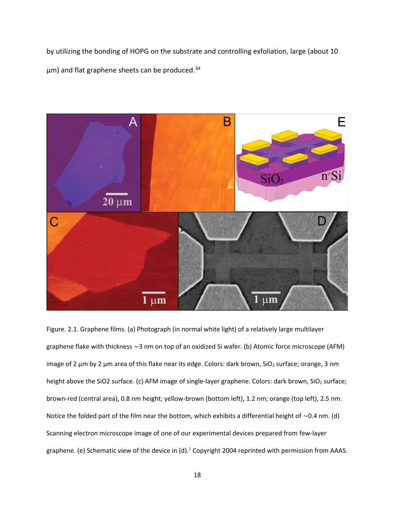
18
by utilizing the bonding of HOPG on the substrate and controlling exfoliation, large (about 10
μm) and flat graphene sheets can be produced.34
Figure. 2.1. Graphene films. (a) Photograph (in normal white light) of a relatively large multilayer
graphene flake with thickness ∼3 nm on top of an oxidized Si wafer. (b) Atomic force microscope (AFM)
image of 2 μm by 2 μm area of this flake near its edge. Colors: dark brown, SiO2 surface; orange, 3 nm
height above the SiO2 surface. (c) AFM image of single-layer graphene. Colors: dark brown, SiO2 surface;
brown-red (central area), 0.8 nm height; yellow-brown (bottom left), 1.2 nm; orange (top left), 2.5 nm.
Notice the folded part of the film near the bottom, which exhibits a differential height of ∼0.4 nm. (d)
Scanning electron microscope image of one of our experimental devices prepared from few-layer
graphene. (e) Schematic view of the device in (d).1 Copyright 2004 reprinted with permission from AAAS.
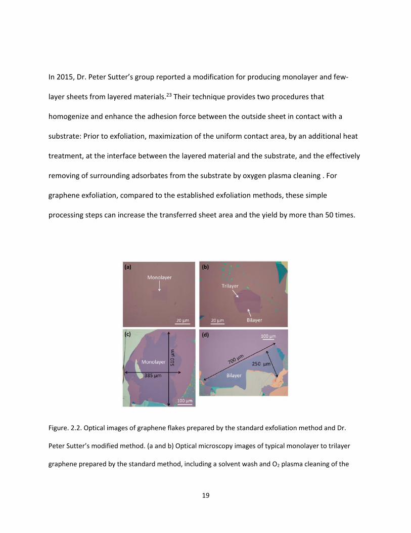
19
In 2015, Dr. Peter Sutter’s group reported a modification for producing monolayer and few-
layer sheets from layered materials.23 Their technique provides two procedures that
homogenize and enhance the adhesion force between the outside sheet in contact with a
substrate: Prior to exfoliation, maximization of the uniform contact area, by an additional heat
treatment, at the interface between the layered material and the substrate, and the effectively
removing of surrounding adsorbates from the substrate by oxygen plasma cleaning . For
graphene exfoliation, compared to the established exfoliation methods, these simple
processing steps can increase the transferred sheet area and the yield by more than 50 times.
Figure. 2.2. Optical images of graphene flakes prepared by the standard exfoliation method and Dr.
Peter Sutter’s modified method. (a and b) Optical microscopy images of typical monolayer to trilayer
graphene prepared by the standard method, including a solvent wash and O2 plasma cleaning of the
20
substrate followed by graphene transfer. (c and d) Optical microscopy images of two graphene flakes
prepared by Dr. Peter Sutter’s modified method, with O2 plasma clean of the SiO2/Si surface, followed by
contact with graphite-loaded tape, annealing to 100 oC, cooling to room temperature and peel-off.23
Copyright 2015 reprinted with permission from American Chemical Society.
The exfoliation method is a very simple method that can provide a high quality, single crystal
sample on many surfaces. Although the modified exfoliation could increase the area to
submillimeter size, the limited size and random shape will limit the potential applications of this
approach. Therefore, it is primarily useful for fundamental research and early stages of
prototype design.
2.2.1.2 Epitaxy
Epitaxial is defined as the directional excessive growth of thin film materials, usually refers to
the growth of single crystal thin films. The first epitaxial graphene was grown by heating a
single crystal of 6H-SiC to a temperature of 1250 to 1400 oC for a short time (1 to 20 minutes) to
thermal decompose Si on the (0001) surface plane.26 This method could effectively grow single
crystal graphene, but it is a challenge to obtain large graphene domains with uniform thickness.
Later, scientist considered the synthesis of graphene on transition metals by epitaxy. In 2008,
Dr. Sutter published a paper about graphene synthesis by thermal cycling of on Ru crystal in
UHV.24 Very sparse graphene nucleation allows the growing of true macroscopic single
crystalline domains with size exceeding 200 μm at high temperatures. Then, epitaxial graphene
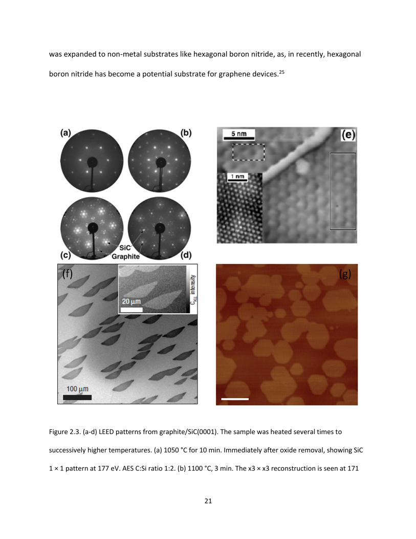
21
was expanded to non-metal substrates like hexagonal boron nitride, as, in recently, hexagonal
boron nitride has become a potential substrate for graphene devices.25
Figure 2.3. (a-d) LEED patterns from graphite/SiC(0001). The sample was heated several times to
successively higher temperatures. (a) 1050 °C for 10 min. Immediately after oxide removal, showing SiC
1 × 1 pattern at 177 eV. AES C:Si ratio 1:2. (b) 1100 °C, 3 min. The x3 × x3 reconstruction is seen at 171
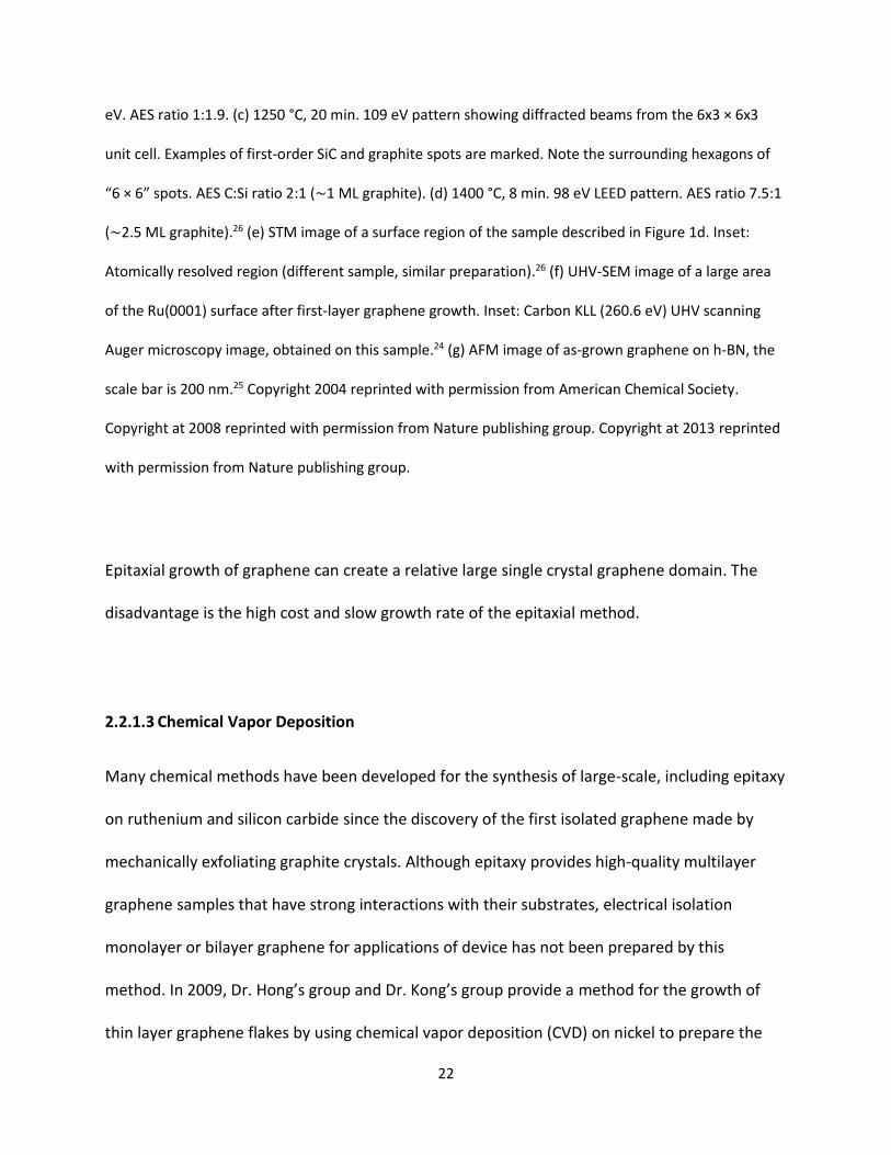
22
eV. AES ratio 1:1.9. (c) 1250 °C, 20 min. 109 eV pattern showing diffracted beams from the 6x3 × 6x3
unit cell. Examples of first-order SiC and graphite spots are marked. Note the surrounding hexagons of
“6 × 6” spots. AES C:Si ratio 2:1 (∼1 ML graphite). (d) 1400 °C, 8 min. 98 eV LEED pattern. AES ratio 7.5:1
(∼2.5 ML graphite).26 (e) STM image of a surface region of the sample described in Figure 1d. Inset:
Atomically resolved region (different sample, similar preparation).26 (f) UHV-SEM image of a large area
of the Ru(0001) surface after first-layer graphene growth. Inset: Carbon KLL (260.6 eV) UHV scanning
Auger microscopy image, obtained on this sample.24 (g) AFM image of as-grown graphene on h-BN, the
scale bar is 200 nm.25 Copyright 2004 reprinted with permission from American Chemical Society.
Copyright at 2008 reprinted with permission from Nature publishing group. Copyright at 2013 reprinted
with permission from Nature publishing group.
Epitaxial growth of graphene can create a relative large single crystal graphene domain. The
disadvantage is the high cost and slow growth rate of the epitaxial method.
2.2.1.3 Chemical Vapor Deposition
Many chemical methods have been developed for the synthesis of large-scale, including epitaxy
on ruthenium and silicon carbide since the discovery of the first isolated graphene made by
mechanically exfoliating graphite crystals. Although epitaxy provides high-quality multilayer
graphene samples that have strong interactions with their substrates, electrical isolation
monolayer or bilayer graphene for applications of device has not been prepared by this
method. In 2009, Dr. Hong’s group and Dr. Kong’s group provide a method for the growth of
thin layer graphene flakes by using chemical vapor deposition (CVD) on nickel to prepare the
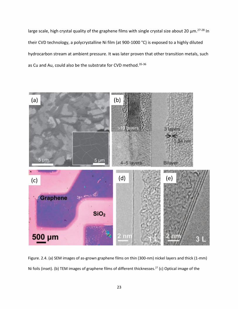
23
large scale, high crystal quality of the graphene films with single crystal size about 20 μm.27-28 In
their CVD technology, a polycrystalline Ni film (at 900-1000 °C) is exposed to a highly diluted
hydrocarbon stream at ambient pressure. It was later proven that other transition metals, such
as Cu and Au, could also be the substrate for CVD method.35-36
Figure. 2.4. (a) SEM images of as-grown graphene films on thin (300-nm) nickel layers and thick (1-mm)
Ni foils (inset). (b) TEM images of graphene films of different thicknesses.27 (c) Optical image of the
24
grown graphene transferred from the Ni surface in panel a to another SiO2/Si substrate. (d-e) High-
magnification TEM images showing the edges of film regions consisting of one (d) and three (e)
graphene layers. The cross-sectional view is enabled by the folding of the film edge. The in-plane lattice
fringes suggest local stacking order of the graphene layers.28 Copyright at 2009 reprinted with
permission from Nature publishing group. Copyright at 2009 reprinted with permission from American
Chemistry Society.
The benefit of the CVD method is that it can create a fully covered and large scale graphene
with a relative easy method and low cost. On the other hand, it is difficult to control the
thickness of the graphene and it can’t be produced as a single crystal sample.
2.2.2 Properties of Graphene
Since graphene has been discovered, it has attracted great attention in many fields of science
due to its impressive properties. The properties of graphene derive from its single atomic
honeycomb structure. From tight-binding theory, we can derive a very unique characteristic of
graphene: a linear energy dispersion relation around the Dirac point. Besides single layer
graphene, the bilayer and trilayer graphene also shows unique properties depending on the
angle between layers.
25
2.2.2.1 Single Layer: Tight-binding Theory
To study the structure of graphene, we have to start with the lattice structure of graphene. The
structure of graphene can be seen as a triangular lattice, each unit cell has two atoms. The
lattice vectors can be written as:
a1 =𝑎
2 (3, √3), a2 =
𝑎
2 (3, −√3),
where a=1.42 Å is the carbon-carbon distance. The reciprocal lattice vectors are given by
b1 =2𝜋
3𝑎(1, √3), b2 =
2𝜋
3𝑎(1, −√3).
The tight binding theory, or tight binding approximation, is a method used to treat a complex
quantum system in solid state physics. Basically, there are there sub-assumptions: (1) consider
only interactions between the frontier atomic orbitals of nearest neighbors; (2) consider only
frontier atomic orbitals; (3) ignore the overlap integrals of separated atoms. By applying this
tight binding theory to the simplest two atom system, we obtain a simple Hamiltonian
equation:
[𝛼1 𝛽𝛽 𝛼2
] [C1
C2] = 𝐸 [
C1
C2]
For graphene, we assume the local potential: ϕ = c1𝜙1 + c2𝜙2 and the wave function: Ψ(��) =
∑ 𝑒𝑖��∙��𝜙(𝑥 − ��)�� , where �� is the lattice vector.
In this graphene system, α1 = α2 = ⟨ϕ𝑗|H|ϕ𝑗⟩, 𝛽 = ⟨ϕ1|H|ϕ2⟩,
We then get two overlap equations:
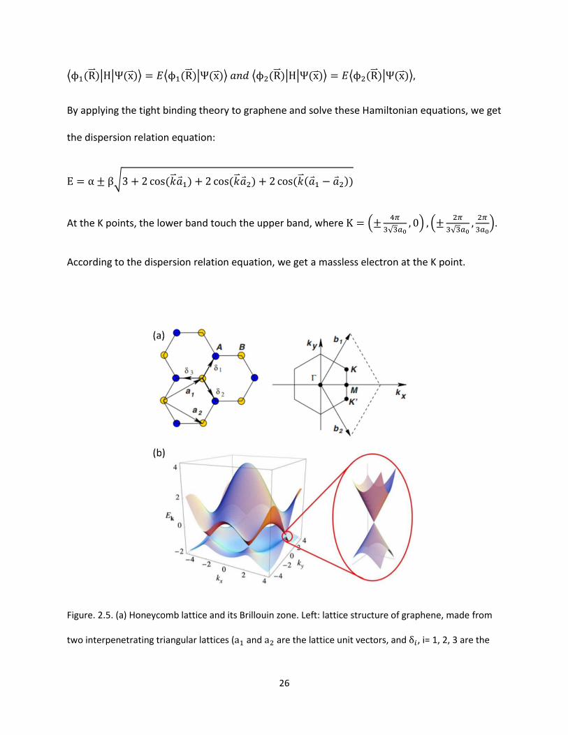
26
⟨ϕ1(R)|H|Ψ(x)⟩ = 𝐸⟨ϕ1(R)|Ψ(x)⟩ 𝑎𝑛𝑑 ⟨ϕ2(R)|H|Ψ(x)⟩ = 𝐸⟨ϕ2(R)|Ψ(x)⟩,
By applying the tight binding theory to graphene and solve these Hamiltonian equations, we get
the dispersion relation equation:
E = α ± β√3 + 2 cos(����1) + 2 cos(����2) + 2 cos(��(��1 − ��2))
At the K points, the lower band touch the upper band, where K = (±4𝜋
3√3𝑎0, 0) , (±
2𝜋
3√3𝑎0,
2𝜋
3𝑎0).
According to the dispersion relation equation, we get a massless electron at the K point.
Figure. 2.5. (a) Honeycomb lattice and its Brillouin zone. Left: lattice structure of graphene, made from
two interpenetrating triangular lattices (a1 and a2 are the lattice unit vectors, and δ𝑖, i= 1, 2, 3 are the
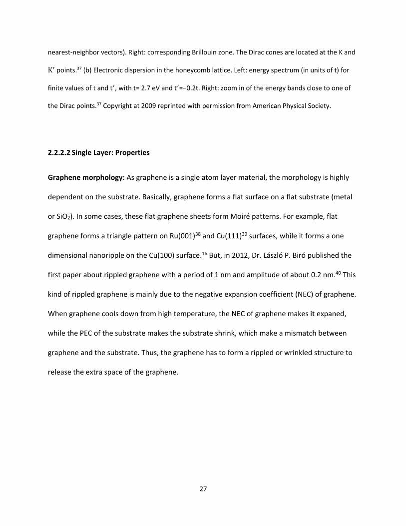
27
nearest-neighbor vectors). Right: corresponding Brillouin zone. The Dirac cones are located at the K and
K′ points.37 (b) Electronic dispersion in the honeycomb lattice. Left: energy spectrum (in units of t) for
finite values of t and t′, with t= 2.7 eV and t′=−0.2t. Right: zoom in of the energy bands close to one of
the Dirac points.37 Copyright at 2009 reprinted with permission from American Physical Society.
2.2.2.2 Single Layer: Properties
Graphene morphology: As graphene is a single atom layer material, the morphology is highly
dependent on the substrate. Basically, graphene forms a flat surface on a flat substrate (metal
or SiO2). In some cases, these flat graphene sheets form Moiré patterns. For example, flat
graphene forms a triangle pattern on Ru(001)38 and Cu(111)39 surfaces, while it forms a one
dimensional nanoripple on the Cu(100) surface.16 But, in 2012, Dr. László P. Biró published the
first paper about rippled graphene with a period of 1 nm and amplitude of about 0.2 nm.40 This
kind of rippled graphene is mainly due to the negative expansion coefficient (NEC) of graphene.
When graphene cools down from high temperature, the NEC of graphene makes it expaned,
while the PEC of the substrate makes the substrate shrink, which make a mismatch between
graphene and the substrate. Thus, the graphene has to form a rippled or wrinkled structure to
release the extra space of the graphene.
28
Figure. 2.6. (a) STM image (170 nm × 170 nm) for graphene grown on Cu(111). A Moire pattern arising
due to the lattice mismatch between graphene and Cu(111) is visible that continues over the step
edges.39 (b) Large area STM topographic image of the rippled graphene showing well-defined linear
periodic modulation with a 0.75 nm spatial modulation frequency (Vs = 0.80 V, I = 1.0 nA).16 (c) STM
image showing several nanotrenches of different orientations, all exhibiting graphene nanoripples over
the trenches with the ripple crests always perpendicular to the trench edges. On the flat regions
between the trenches, a Moiré pattern can be observed.40 (d) Atomic-resolution STM image of a
nanotrench exhibiting subnanometer graphene ripples. The magnified insets exhibit the honeycomb
graphene lattice both over the flat substrate (bottom right) and the rippled region over the trenches
29
(top left).40 Copyright at 2015 reprinted with permission from American Chemical Society. Copyright at
2015 reprinted with permission from Nature publishing group. Copyright at 2012 reprinted with
permission from Nature publishing group.
Electronic properties: The experimental observation that the mass of the cyclotron depends on
the square root of the electronic density of graphene is explained as the evidence of the
presence of massless Dirac quasiparticles in graphene.41 Owing to its unique band structure,
graphene exhibits novel transport effects such as ambipolar field effect and minimum
conductivity which are absent in most conventional materials, with a concentration up to 1013
cm−2 and a mobility of as high as 15 000 cm2V−1s−1 at room temperature, which is much higher
than the concentration (1010 cm-2) and mobility (1400 cm2V−1s−1) of silicon.1, 42 Mobility of
suspended graphene exceeds 200 000 cm2V−1s−1 by minimizing impurity scattering.43
Mechanical properties: The mechanical properties of monolayer graphene have been well
predicted by first principles based calculations, including the Young's modulus and fracture
strength.41 A direct measurement of mechanical properties of monolayer graphene was first
reported by Lee et al.44, by nanoindentation of suspended monolayer graphene membranes
using an atomic microscope (AFM). By force‐volume measurements in AFM, few‐layer
graphene circular membranes were also characterized.45 Recently, by the nanoindentation
method using an AFM, the inherent fracture strength and elasticity of free standing monolayer
graphene were measured (Figure 2.7a and b).46 It was reported that the Young's modulus of
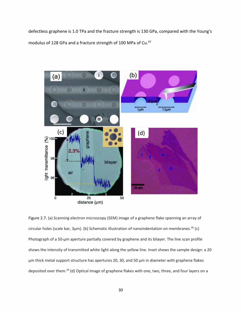
30
defectless graphene is 1.0 TPa and the fracture strength is 130 GPa, compared with the Young's
modulus of 128 GPa and a fracture strength of 100 MPa of Cu.47
Figure 2.7. (a) Scanning electron microscopy (SEM) image of a graphene flake spanning an array of
circular holes (scale bar, 3μm). (b) Schematic illustration of nanoindentation on membranes.46 (c)
Photograph of a 50‐μm aperture partially covered by graphene and its bilayer. The line scan profile
shows the intensity of transmitted white light along the yellow line. Inset shows the sample design: a 20
μm thick metal support structure has apertures 20, 30, and 50 μm in diameter with graphene flakes
deposited over them.29 (d) Optical image of graphene flakes with one, two, three, and four layers on a
31
285‐nm thick SiO2‐on‐Si substrate.48 Copyright at 2008 reprinted with permission from AAAS. Copyright
at 2008 reprinted with permission from AAAS. Copyright at 2007 reprinted with permission from
American Chemical Society.
Optical properties: From the infrared to the visible range of the spectrum, the high frequency
conductivity of Dirac fermions in graphene has been expressed as a constant of πe2/2h.49-50
Then for normal incidence light, the reflectance R and transmittance T are then R = 1/4π2α2T
and T = (1 + 1/2πα)−2; the opacity is (1 − T) ≈ πα ≈ 2.3% (where α = 2πe2/hc ≈ 1/137, h is
Planck's constant, c the light speed, and e the electron charge). It is considered as the result of
the electronic and structure properties of graphene that the expression of R and T in terms of
basic constants instead of involving parameters of graphene.51 As shown in Figure 2.7c, it is
experimentally observed that graphene in the visible light range has a constant transparency
(about 97.7%), as well as the transmittance decreases proportionally with the number of
graphene layers, while the transparency of indium tin oxide (ITO, a common transparent
electrode) is around 85%.29
2.2.2.3 Bilayer and Trilayer Graphene
Monolayer graphene owns a linear energy dispersion near the Dirac points. Their bands
hybridized due to hopping results of interlayer in a fundamental modification to the low energy
band structure depending on the stacking order (AA (carbon atoms of both layers have identical
lateral coordinates) or AB (the second graphene layer is shifted relative to the first one by the
32
vector equal to the edge of the hexagon)), when two aligned graphene sheets are stacked. A
hexagonal moiré pattern consisting of alternating AB- and AA-stacked regions appears and acts
as a superlattice modulation, if there is an additional twist angle between layers. For example,
the band structure of twisted bilayer graphene can be customized to create a bandgap and
band curvatures that would not otherwise exist. In 2018, Yuan Cao et al. pulished two papers
related to twisted bilayer exist. In one paper, observation of superconductivity of bilayer
graphene with slightly different twist angles has been reported, with the maximum critical
temperature of 1.7 K.52 In the other paper, they experimentally demonstrate that the interlayer
hybridization can induce almost flat low-energy bands when the twist angle of twisted bilayer
graphene is close to the magic angle predicted by theory.53 A insulating phase at half filling of
these flat bands is led by this quenching of the quantum kinetic energy, which indicates a Mott-
like insulator in the localized flat bands.53 After the publication of these two papers, there was
intense investigation of twisted bilayer or trilayer two-dimensional materials.54
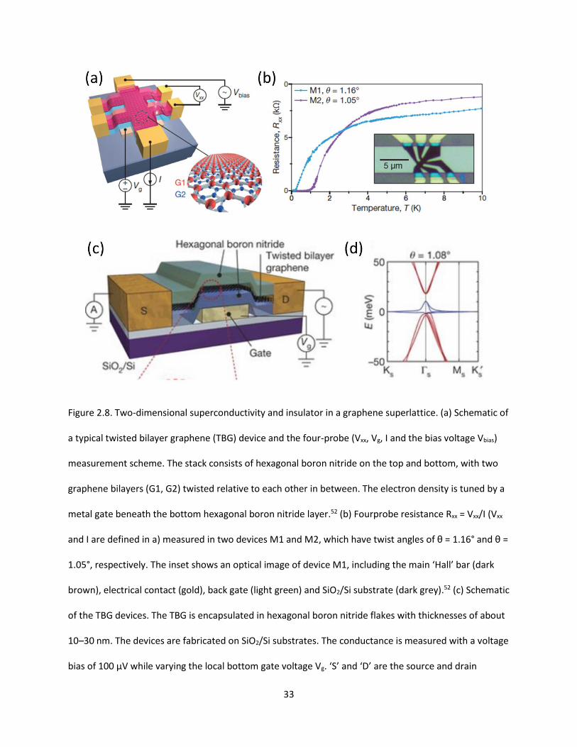
33
Figure 2.8. Two-dimensional superconductivity and insulator in a graphene superlattice. (a) Schematic of
a typical twisted bilayer graphene (TBG) device and the four-probe (Vxx, Vg, I and the bias voltage Vbias)
measurement scheme. The stack consists of hexagonal boron nitride on the top and bottom, with two
graphene bilayers (G1, G2) twisted relative to each other in between. The electron density is tuned by a
metal gate beneath the bottom hexagonal boron nitride layer.52 (b) Fourprobe resistance Rxx = Vxx/I (Vxx
and I are defined in a) measured in two devices M1 and M2, which have twist angles of θ = 1.16° and θ =
1.05°, respectively. The inset shows an optical image of device M1, including the main ‘Hall’ bar (dark
brown), electrical contact (gold), back gate (light green) and SiO2/Si substrate (dark grey).52 (c) Schematic
of the TBG devices. The TBG is encapsulated in hexagonal boron nitride flakes with thicknesses of about
10–30 nm. The devices are fabricated on SiO2/Si substrates. The conductance is measured with a voltage
bias of 100 μV while varying the local bottom gate voltage Vg. ‘S’ and ‘D’ are the source and drain
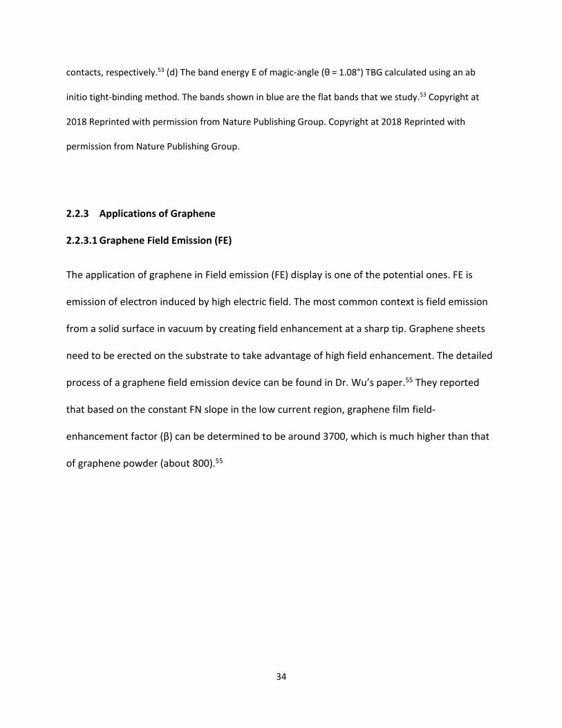
34
contacts, respectively.53 (d) The band energy E of magic-angle (θ = 1.08°) TBG calculated using an ab
initio tight-binding method. The bands shown in blue are the flat bands that we study.53 Copyright at
2018 Reprinted with permission from Nature Publishing Group. Copyright at 2018 Reprinted with
permission from Nature Publishing Group.
2.2.3 Applications of Graphene
2.2.3.1 Graphene Field Emission (FE)
The application of graphene in Field emission (FE) display is one of the potential ones. FE is
emission of electron induced by high electric field. The most common context is field emission
from a solid surface in vacuum by creating field enhancement at a sharp tip. Graphene sheets
need to be erected on the substrate to take advantage of high field enhancement. The detailed
process of a graphene field emission device can be found in Dr. Wu’s paper.55 They reported
that based on the constant FN slope in the low current region, graphene film field-
enhancement factor (β) can be determined to be around 3700, which is much higher than that
of graphene powder (about 800).55
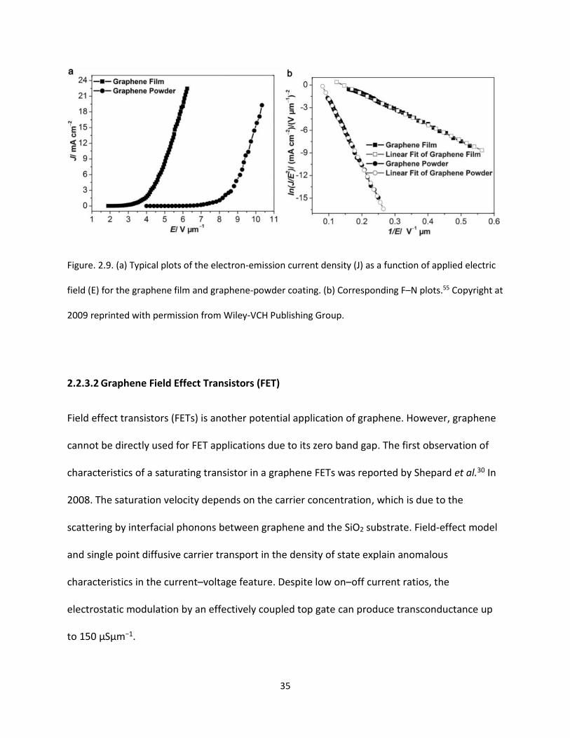
35
Figure. 2.9. (a) Typical plots of the electron-emission current density (J) as a function of applied electric
field (E) for the graphene film and graphene-powder coating. (b) Corresponding F–N plots.55 Copyright at
2009 reprinted with permission from Wiley-VCH Publishing Group.
2.2.3.2 Graphene Field Effect Transistors (FET)
Field effect transistors (FETs) is another potential application of graphene. However, graphene
cannot be directly used for FET applications due to its zero band gap. The first observation of
characteristics of a saturating transistor in a graphene FETs was reported by Shepard et al.30 In
2008. The saturation velocity depends on the carrier concentration, which is due to the
scattering by interfacial phonons between graphene and the SiO2 substrate. Field-effect model
and single point diffusive carrier transport in the density of state explain anomalous
characteristics in the current–voltage feature. Despite low on–off current ratios, the
electrostatic modulation by an effectively coupled top gate can produce transconductance up
to 150 µSµm−1.
36
Figure. 2.10. (a) Schematic of a graphene FET on a Si/SiO2 substrate with a heavily doped Si wafer acting
as a back gate and a gold top gate. (b) SEM micrograph showing a representative graphene top-gated
FET. The top-gate of this device is 1 µm long, with 3 µm spacing between the source–drain contacts. All
electrodes are Cr/Au. (c) Drain current (Id) as a function of source-to-drain voltage (Vsd) for Vgs-top = −0.3
V, −0.8 V, −1.3 V, −1.8 V, −2.3 V and −2.8 V (from bottom to top) for Vgs-back = 40 V. (d) Id as a function of
Vsd for Vgs-top = −0.3 V, −0.8 V, −1.3 V, −1.8 V, −2.3 V and −2.8 V (from bottom to top) for Vgs-back = −40 V.30
Copyright at 2008 reprinted with permission from Nature Publishing Group.
37
2.2.3.3 Graphene-based Gas and Biological Sensors
Graphene-based sensors, including gas and biological sensors, is one of the most prospective
applications.56 The working theory of a graphene-based gas and biological sensors is based on
changes in conductivity of graphene and the molecular adsorption on the surface of graphene.
The change of conductivity of the graphene is mainly because of the absorbed gas molecules
working like acceptors or donors can create the change in electrical conductivity. In addition,
some interesting properties of graphene help increase the sensitivity to the detection of
individual atoms or molecules. First, graphene is a two-dimensional material whose entire
volume is exposed to the target analyte. Then, graphene has high conductivity and low Johnson
noise, therefore, a significant change of conductivity can be caused by a variation in carrier
concentration. What’s more, graphene has almost no crystal defects, ensuring a low level of
thermal switching noise. In the end, four-probe measurements can be made on single crystal
graphene device with low resistance ohmic electrical contacts. One of the influential papers
that demonstrate a gas sensor using a graphene sheet was published in 2011.57 In this paper, a
high performance carbon dioxide (CO2) gas sensor is reported of graphene made by exfoliation.
The graphene sensor can be operated at room temperature and under ambient conditions,
unlike other solid-state gas sensors. For a variety of concentrations of CO2 gas adsorbed on the
surface of graphene, the change in the conductance of the device was measured. With the
increasing concentration of CO2 gas, the conductivity of the graphene gas sensor increases
linearly. The advantages of this sensor are fast response time, high sensitivity, low power
consumption, and short recovery time.
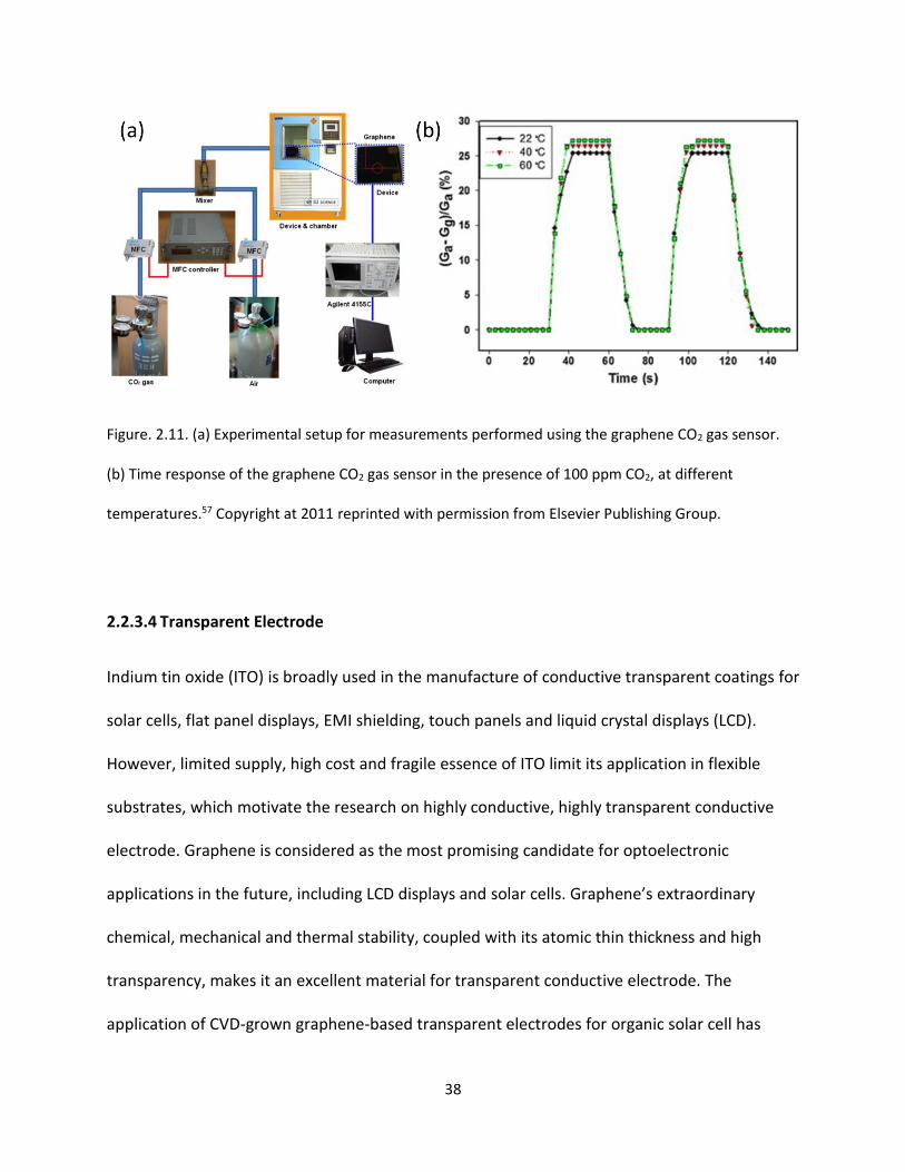
38
Figure. 2.11. (a) Experimental setup for measurements performed using the graphene CO2 gas sensor.
(b) Time response of the graphene CO2 gas sensor in the presence of 100 ppm CO2, at different
temperatures.57 Copyright at 2011 reprinted with permission from Elsevier Publishing Group.
2.2.3.4 Transparent Electrode
Indium tin oxide (ITO) is broadly used in the manufacture of conductive transparent coatings for
solar cells, flat panel displays, EMI shielding, touch panels and liquid crystal displays (LCD).
However, limited supply, high cost and fragile essence of ITO limit its application in flexible
substrates, which motivate the research on highly conductive, highly transparent conductive
electrode. Graphene is considered as the most promising candidate for optoelectronic
applications in the future, including LCD displays and solar cells. Graphene’s extraordinary
chemical, mechanical and thermal stability, coupled with its atomic thin thickness and high
transparency, makes it an excellent material for transparent conductive electrode. The
application of CVD-grown graphene-based transparent electrodes for organic solar cell has
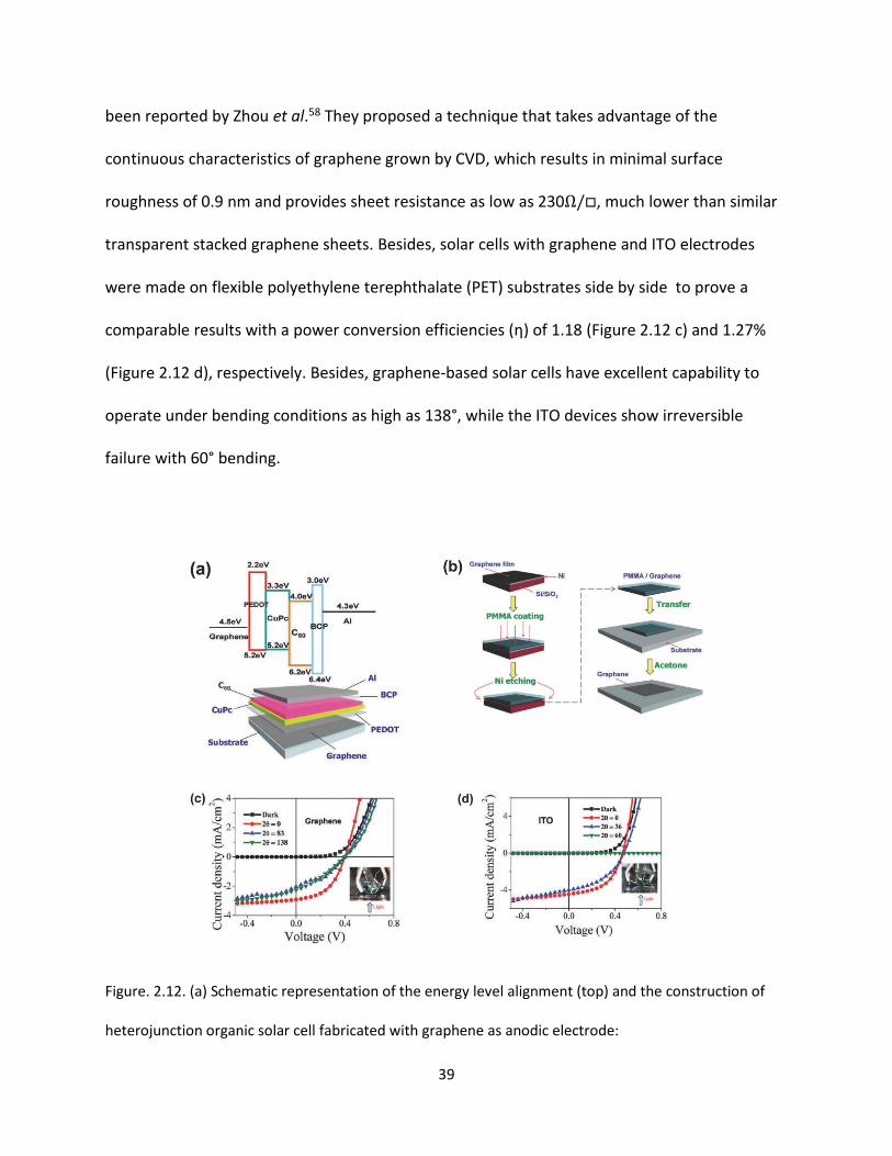
39
been reported by Zhou et al.58 They proposed a technique that takes advantage of the
continuous characteristics of graphene grown by CVD, which results in minimal surface
roughness of 0.9 nm and provides sheet resistance as low as 230Ω/□, much lower than similar
transparent stacked graphene sheets. Besides, solar cells with graphene and ITO electrodes
were made on flexible polyethylene terephthalate (PET) substrates side by side to prove a
comparable results with a power conversion efficiencies (η) of 1.18 (Figure 2.12 c) and 1.27%
(Figure 2.12 d), respectively. Besides, graphene-based solar cells have excellent capability to
operate under bending conditions as high as 138°, while the ITO devices show irreversible
failure with 60° bending.
Figure. 2.12. (a) Schematic representation of the energy level alignment (top) and the construction of
heterojunction organic solar cell fabricated with graphene as anodic electrode:
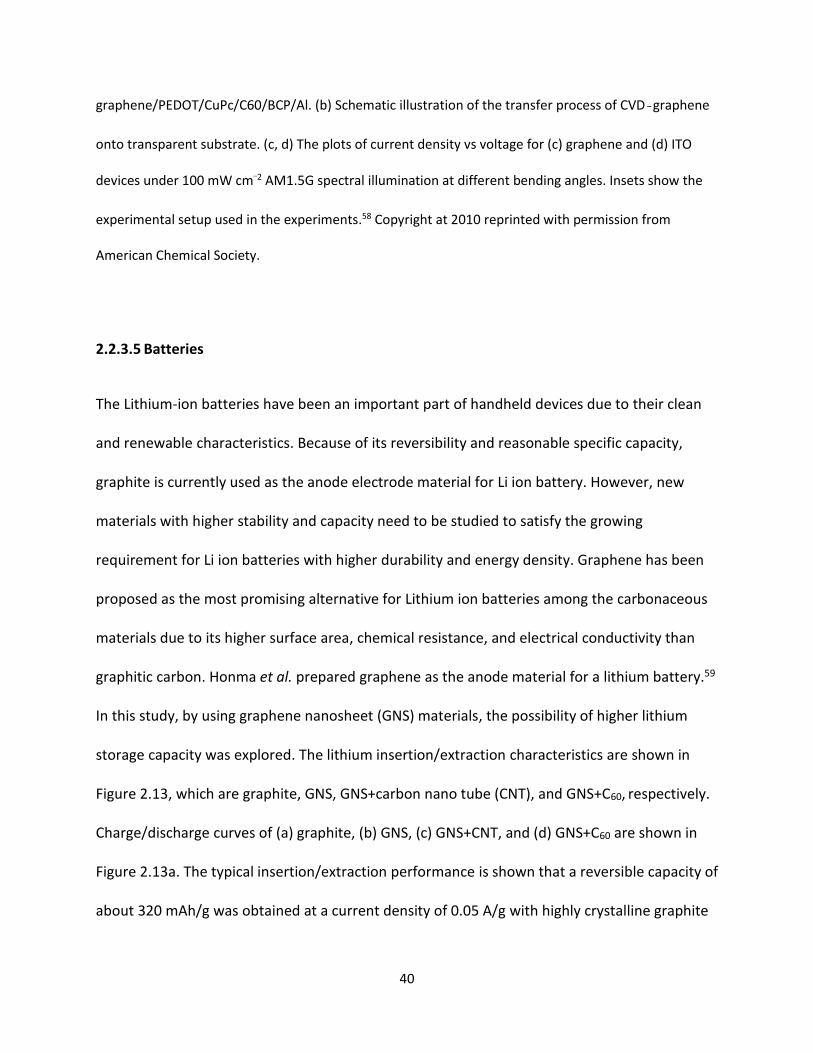
40
graphene/PEDOT/CuPc/C60/BCP/Al. (b) Schematic illustration of the transfer process of CVD‐graphene
onto transparent substrate. (c, d) The plots of current density vs voltage for (c) graphene and (d) ITO
devices under 100 mW cm–2 AM1.5G spectral illumination at different bending angles. Insets show the
experimental setup used in the experiments.58 Copyright at 2010 reprinted with permission from
American Chemical Society.
2.2.3.5 Batteries
The Lithium-ion batteries have been an important part of handheld devices due to their clean
and renewable characteristics. Because of its reversibility and reasonable specific capacity,
graphite is currently used as the anode electrode material for Li ion battery. However, new
materials with higher stability and capacity need to be studied to satisfy the growing
requirement for Li ion batteries with higher durability and energy density. Graphene has been
proposed as the most promising alternative for Lithium ion batteries among the carbonaceous
materials due to its higher surface area, chemical resistance, and electrical conductivity than
graphitic carbon. Honma et al. prepared graphene as the anode material for a lithium battery.59
In this study, by using graphene nanosheet (GNS) materials, the possibility of higher lithium
storage capacity was explored. The lithium insertion/extraction characteristics are shown in
Figure 2.13, which are graphite, GNS, GNS+carbon nano tube (CNT), and GNS+C60, respectively.
Charge/discharge curves of (a) graphite, (b) GNS, (c) GNS+CNT, and (d) GNS+C60 are shown in
Figure 2.13a. The typical insertion/extraction performance is shown that a reversible capacity of
about 320 mAh/g was obtained at a current density of 0.05 A/g with highly crystalline graphite
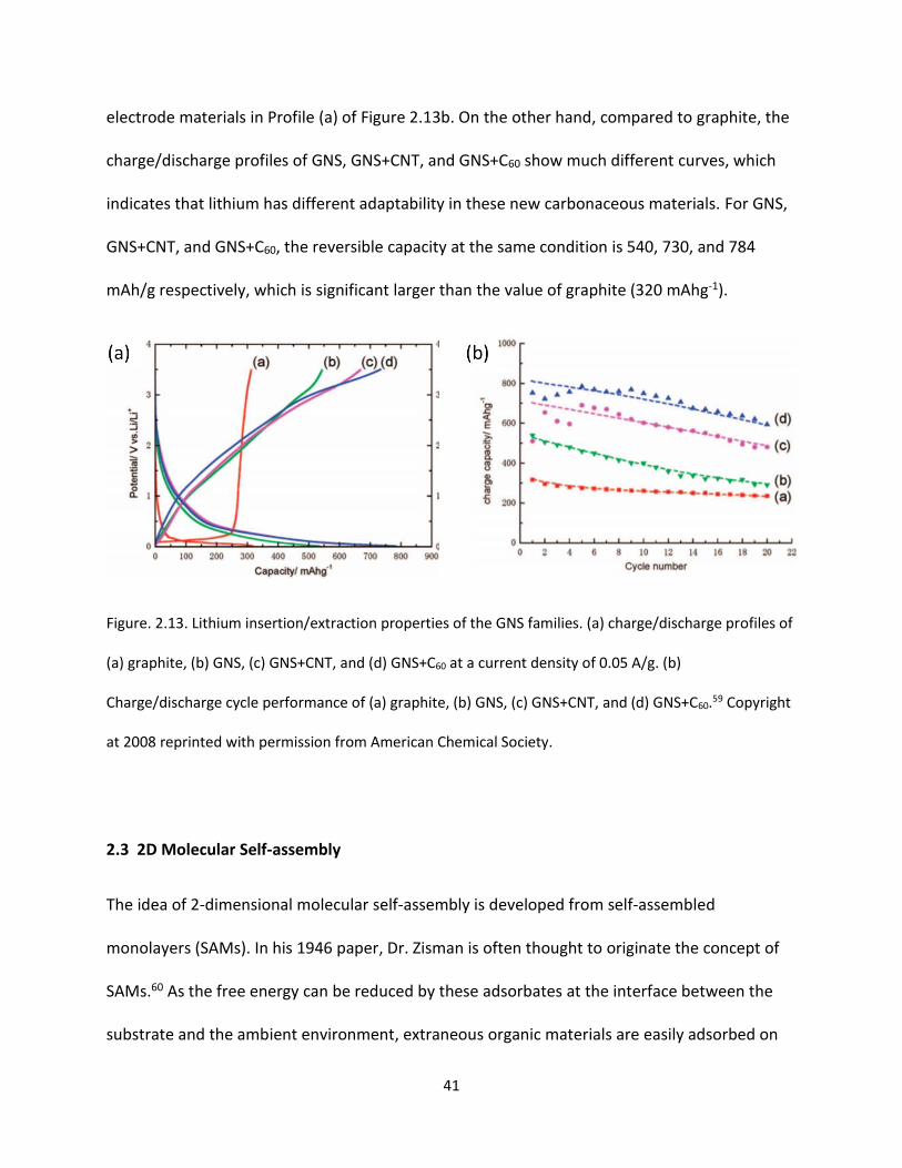
41
electrode materials in Profile (a) of Figure 2.13b. On the other hand, compared to graphite, the
charge/discharge profiles of GNS, GNS+CNT, and GNS+C60 show much different curves, which
indicates that lithium has different adaptability in these new carbonaceous materials. For GNS,
GNS+CNT, and GNS+C60, the reversible capacity at the same condition is 540, 730, and 784
mAh/g respectively, which is significant larger than the value of graphite (320 mAhg-1).
Figure. 2.13. Lithium insertion/extraction properties of the GNS families. (a) charge/discharge profiles of
(a) graphite, (b) GNS, (c) GNS+CNT, and (d) GNS+C60 at a current density of 0.05 A/g. (b)
Charge/discharge cycle performance of (a) graphite, (b) GNS, (c) GNS+CNT, and (d) GNS+C60.59 Copyright
at 2008 reprinted with permission from American Chemical Society.
2.3 2D Molecular Self-assembly
The idea of 2-dimensional molecular self-assembly is developed from self-assembled
monolayers (SAMs). In his 1946 paper, Dr. Zisman is often thought to originate the concept of
SAMs.60 As the free energy can be reduced by these adsorbates at the interface between the
substrate and the ambient environment, extraneous organic materials are easily adsorbed on
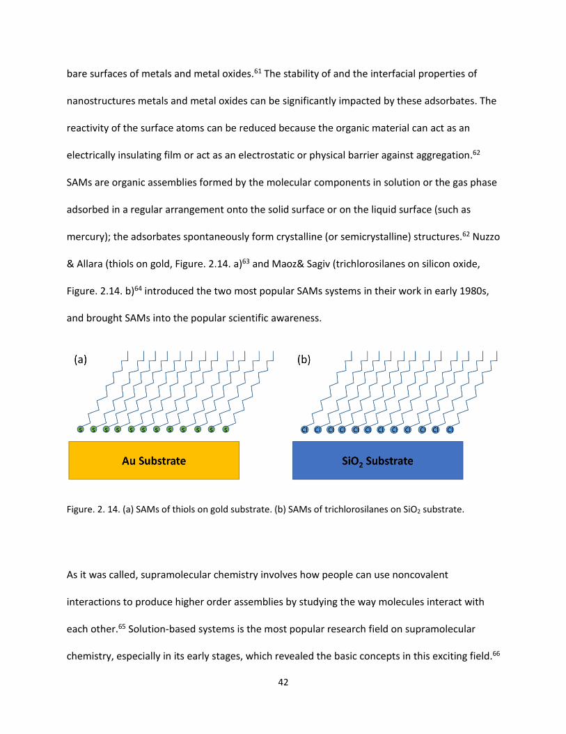
42
bare surfaces of metals and metal oxides.61 The stability of and the interfacial properties of
nanostructures metals and metal oxides can be significantly impacted by these adsorbates. The
reactivity of the surface atoms can be reduced because the organic material can act as an
electrically insulating film or act as an electrostatic or physical barrier against aggregation.62
SAMs are organic assemblies formed by the molecular components in solution or the gas phase
adsorbed in a regular arrangement onto the solid surface or on the liquid surface (such as
mercury); the adsorbates spontaneously form crystalline (or semicrystalline) structures.62 Nuzzo
& Allara (thiols on gold, Figure. 2.14. a)63 and Maoz& Sagiv (trichlorosilanes on silicon oxide,
Figure. 2.14. b)64 introduced the two most popular SAMs systems in their work in early 1980s,
and brought SAMs into the popular scientific awareness.
Figure. 2. 14. (a) SAMs of thiols on gold substrate. (b) SAMs of trichlorosilanes on SiO2 substrate.
As it was called, supramolecular chemistry involves how people can use noncovalent
interactions to produce higher order assemblies by studying the way molecules interact with
each other.65 Solution-based systems is the most popular research field on supramolecular
chemistry, especially in its early stages, which revealed the basic concepts in this exciting field.66
43
After the discovery of STM, it was soon used in the field of SAMs and supramolecular self-
assembly on surfaces due to its atomic scale high spatial resolution, which forms a new field
called 2D molecular self-assembly.67 In particular, STM is extremely useful to probe the
electronic properties of the surface molecule and not only the organization of molecular
surface dynamics , but also of molecules on a local scale during the self-assembly process.
2D molecular self-assembly usually means the molecules form a two-dimensional structure on a
surface, such as a metal or, more recently, graphene. Self‐assembly of molecules at a surface
depends mainly on two kinds of interactions: non‐covalent molecule‐molecule interaction
defining the relationship between neighboring molecules, and molecule‐substrate interaction
stabilizing the molecules on the surface. Many different intermolecular interactions can form
2D self‐assembly. Strong hydrogen bonds (such as carboxylic dimers) and strong directional
bonds including coordination at metal centers can produce porous assembly structures.
Generally, weaker bonds (such as van der Waals interactions and halogen‐halogen) result in a
close‐packed structure with the maximized areal molecular density. We will discuss molecular
self-assembly with these four interactions, respectively.
2.3.1 Metal Bonds Molecular Self-assembly
Metal bonds molecular self-assembly usually describe the 2D frameworks of a heterogeneous
system of metal and organic molecules by the metal-directed bonding, such as metal-
carboxylates bonding. It provided a new way to study the heterogenous system, including
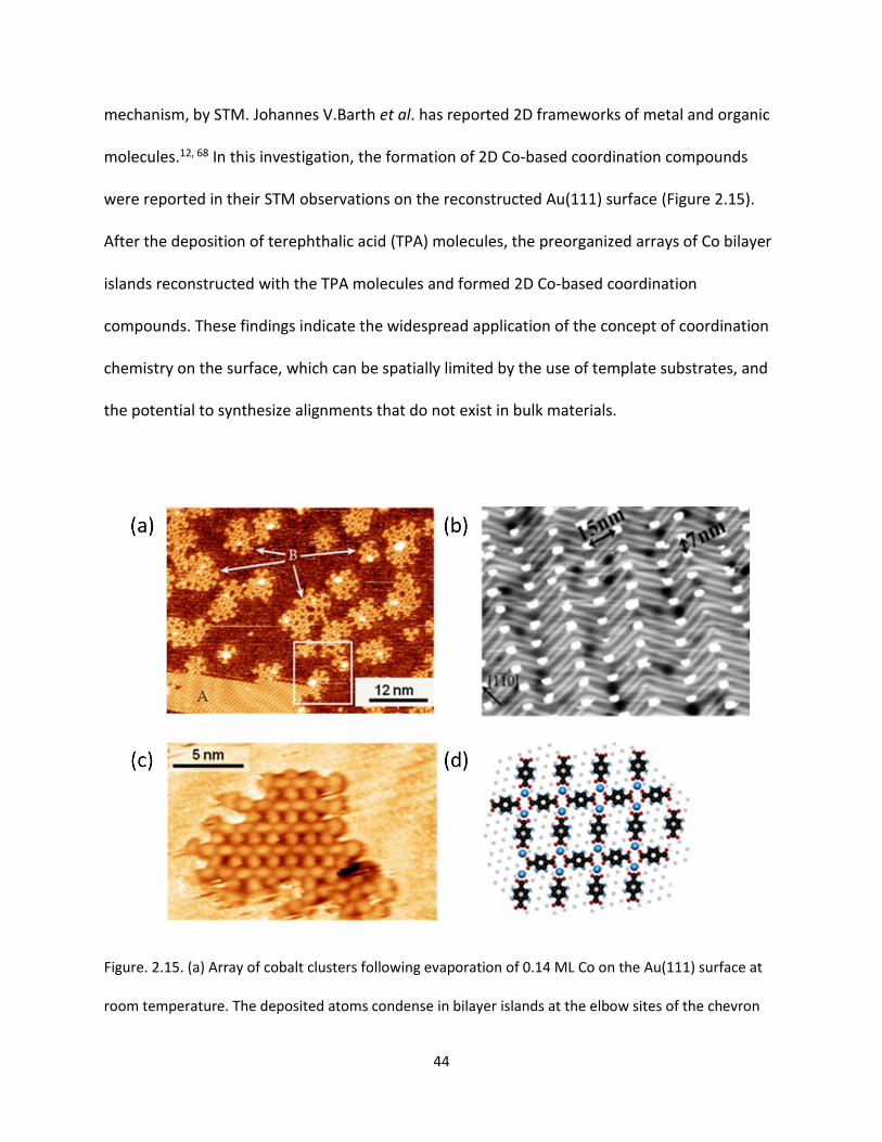
44
mechanism, by STM. Johannes V.Barth et al. has reported 2D frameworks of metal and organic
molecules.12, 68 In this investigation, the formation of 2D Co-based coordination compounds
were reported in their STM observations on the reconstructed Au(111) surface (Figure 2.15).
After the deposition of terephthalic acid (TPA) molecules, the preorganized arrays of Co bilayer
islands reconstructed with the TPA molecules and formed 2D Co-based coordination
compounds. These findings indicate the widespread application of the concept of coordination
chemistry on the surface, which can be spatially limited by the use of template substrates, and
the potential to synthesize alignments that do not exist in bulk materials.
Figure. 2.15. (a) Array of cobalt clusters following evaporation of 0.14 ML Co on the Au(111) surface at
room temperature. The deposited atoms condense in bilayer islands at the elbow sites of the chevron
45
reconstruction. The Co dots contain on the average ∼200 atoms representing in situ nano-reservoirs for
the formation of metal-organic complexes with co-deposited carboxylic acids (STM image size 100 × 80
nm2, I =1.3 nA, V = 20 mV). (b) Complexation reaction following deposition of 0.3 ML TPA on a Co array
(0.08 ML, corresponding to ∼120 atoms per island) on Au(111) at room temperature. A minority of
hydrogen-bonded domains (A) coexists with the dominating metal-organic compounds (B) evolving
around residual Co dots (I = 0.6 nA, V = -0.7 V). (b) Array of cobalt clusters following evaporation of 0.14
ML Co on the Au(111) surface at room temperature. The deposited atoms condense in bilayer islands at
the elbow sites of the chevron reconstruction. The Co dots contain on the average ∼200 atoms
representing in situ nano-reservoirs for the formation of metal-organic complexes with co-deposited
carboxylic acids (STM image size 100 × 80 nm2, I = 1.3 nA, V = 20 mV). (c) Fully developed rectangular
metal–organic nanogrid with a Co–TPA stoichiometry of 1:1 following annealing at 330 K. (d) The model
at the right depicts the underlying dicobalt coordination motif with both axial chelating and equatorial
bridging metal center–carboxylate bonds.68 Copyright at 2009 reprinted with permission from Elsevier
Publishing Group.
2.3.2 Hydrogen Bonding Molecular Self-assembly
Hydrogen bonding is the main electrostatic attraction between a hydrogen (H) atom (the
hydrogen bond acceptor) and the second-row elements oxygen (O), fluorine (F), or nitrogen (N)
(the hydrogen bond donor).69 It is one of the most fundamental non-covalent forces in both
artificial systems (various soft materials, molecular self-assembly, etc.) and biological (DNA,
saccharides etc.). 2D molecular self-assembly is one of the best ways to investigate the
hydrogen bonding between molecules as we can directly ‘see’ the bonding between two atoms
by STM. In 2010, Perepichka published a review on supramolecular design with carboxylic
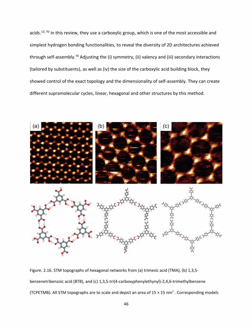
46
acids.13, 70 In this review, they use a carboxylic group, which is one of the most accessible and
simplest hydrogen bonding functionalities, to reveal the diversity of 2D architectures achieved
through self-assembly.70 Adjusting the (i) symmetry, (ii) valency and (iii) secondary interactions
(tailored by substituents), as well as (iv) the size of the carboxylic acid building block, they
showed control of the exact topology and the dimensionality of self-assembly. They can create
different supramolecular cycles, linear, hexagonal and other structures by this method.
Figure. 2.16. STM topographs of hexagonal networks from (a) trimesic acid (TMA), (b) 1,3,5-
benzenetribenzoic acid (BTB), and (c) 1,3,5-tri(4-carboxyphenylethynyl)-2,4,6-trimethylbenzene
(TCPETMB). All STM topographs are to scale and depict an area of 15 × 15 nm2 . Corresponding models
47
of a single supramolecular cavity bordered by six molecules are depicted below and demonstrate the
underlying building plan of these isotopological networks with dimers interconnected by 2-fold
hydrogen bonds between carboxylic groups as a structural unit.13 Copyright at 2009 reprinted with
permission from American Chemical Society.
2.3.3 Van der Waals Molecular Self-assembly
The van der Waals force is a distance-dependent force between molecules or atoms in
nanoscale physics, named after scientist Johannes Diderik van der Waals. This attraction does
not caused by chemical electronic bonds, compared to ionic or covalent bonds; it is relatively
weak, and so more impacted by disturbance.71 The Van der Waals force significantly decrease
at longer gap between interacting molecules or atoms.71 The Van der Waals force plays an
important role in many fields such as molecular self-assembly, structural biology,
nanotechnology, polymer science, condensed matter physics, and surface science. The Van Der
Waals interaction is the mechanism behind the self-assembly of the fullerene family, like C60
and Gd3@C80 (metallofulerene). The first STM images of ordered C60 were reported by Richard J.
Colton in 1993,14 while the first STM images of a metallofullerene was published by G.A.D.
Briggs in 2008 as the discover of metallofullerene is much later than C60.72
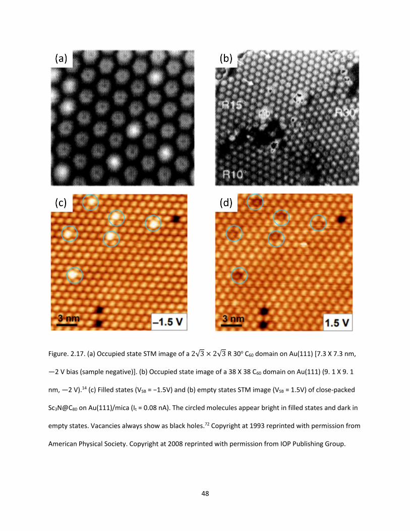
48
Figure. 2.17. (a) Occupied state STM image of a 2√3 × 2√3 R 30o C60 domain on Au(111) [7.3 X 7.3 nm,
—2 V bias (sample negative)]. (b) Occupied state image of a 38 X 38 C60 domain on Au(111) (9. 1 X 9. 1
nm, —2 V).14 (c) Filled states (VSB = −1.5V) and (b) empty states STM image (VSB = 1.5V) of close-packed
Sc3N@C80 on Au(111)/mica (It = 0.08 nA). The circled molecules appear bright in filled states and dark in
empty states. Vacancies always show as black holes.72 Copyright at 1993 reprinted with permission from
American Physical Society. Copyright at 2008 reprinted with permission from IOP Publishing Group.
49
2.3.4 Halogen‐halogen Molecular Self-assembly
Halogen bonding is very similar to hydrogen bonding. A similar relationship can easily be get
between hydrogen and halogen bonding. There is an electron acceptor and donor relationship
in both types of bonding. The species, which acts as the electron donor or acceptor, is the only
difference between these two bonding. In halogen bonding, a halogen atom forms a non-
covalent interaction by acting as the electron acceptor and accepting density of electron from
an electron donor.73 While in hydrogen bonding, a hydrogen atom is the electron acceptor. At
the same time, the covalent bond between halogen atom (X) or hydrogen atom (H) and other
atom (D) weakens, therefore the electron density on X or H is reduced.73 Electron density
transfer leads to a penetration of the Van der Waals volumes. Recently, a paper discussed the
self-assembly behavior of hexakis(4-iodophenyl)benzene (HPBI) through the halogen-halogen
bonding.15 In this investigation, they report a D6h symmetric molecule HPBI, is used as a basis
component to build two types of periodic self-assembly phases on Au(111). These self-assembly
phases have the different packing densities but same lattice symmetry; the change in packing
density is due to networks build by halogen bonds74-75 and halogen–Au coordination, as
confirmed by STM experiment and DFT calculations. It is worth noting that the self-similarity of
these two patterns facilitates the interweaving of the patterns to form higher order self-
assembly phases. This mechanism provides a new method for building complex 2D mosaics
through intermolecular interactions and molecular-substrate interactions.76-77
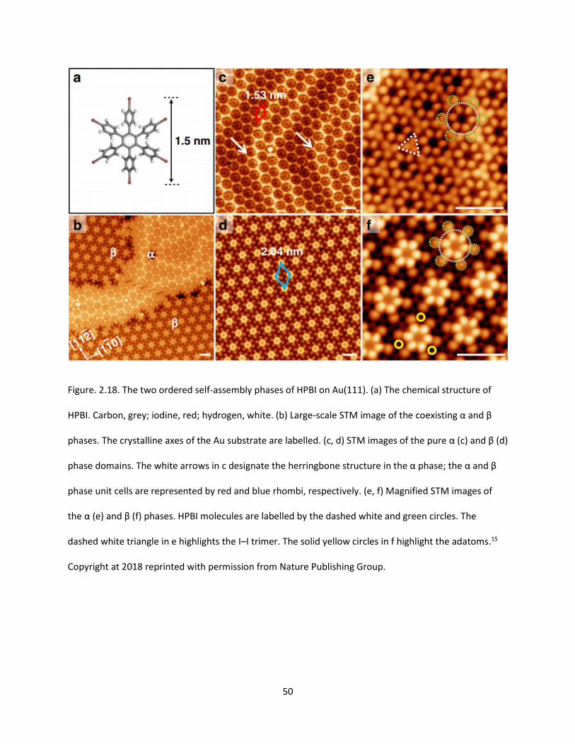
50
Figure. 2.18. The two ordered self-assembly phases of HPBI on Au(111). (a) The chemical structure of
HPBI. Carbon, grey; iodine, red; hydrogen, white. (b) Large-scale STM image of the coexisting α and β
phases. The crystalline axes of the Au substrate are labelled. (c, d) STM images of the pure α (c) and β (d)
phase domains. The white arrows in c designate the herringbone structure in the α phase; the α and β
phase unit cells are represented by red and blue rhombi, respectively. (e, f) Magnified STM images of
the α (e) and β (f) phases. HPBI molecules are labelled by the dashed white and green circles. The
dashed white triangle in e highlights the I–I trimer. The solid yellow circles in f highlight the adatoms.15
Copyright at 2018 reprinted with permission from Nature Publishing Group.
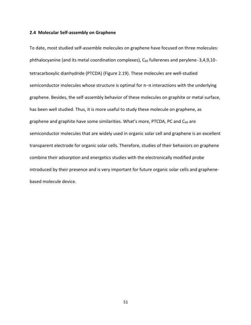
51
2.4 Molecular Self-assembly on Graphene
To date, most studied self-assemble molecules on graphene have focused on three molecules:
phthalocyanine (and its metal coordination complexes), C60 fullerenes and perylene‐3,4,9,10‐
tetracarboxylic dianhydride (PTCDA) (Figure 2.19). These molecules are well-studied
semiconductor molecules whose structure is optimal for π−π interactions with the underlying
graphene. Besides, the self-assembly behavior of these molecules on graphite or metal surface,
has been well studied. Thus, it is more useful to study these molecule on graphene, as
graphene and graphite have some similarities. What’s more, PTCDA, PC and C60 are
semiconductor molecules that are widely used in organic solar cell and graphene is an excellent
transparent electrode for organic solar cells. Therefore, studies of their behaviors on graphene
combine their adsorption and energetics studies with the electronically modified probe
introduced by their presence and is very important for future organic solar cells and graphene-
based molecule device.
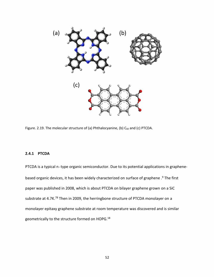
52
Figure. 2.19. The molecular structure of (a) Phthalocyanine, (b) C60 and (c) PTCDA.
2.4.1 PTCDA
PTCDA is a typical n‐type organic semiconductor. Due to its potential applications in graphene-
based organic devices, it has been widely characterized on surface of graphene .9 The first
paper was published in 2008, which is about PTCDA on bilayer graphene grown on a SiC
substrate at 4.7K.78 Then in 2009, the herringbone structure of PTCDA monolayer on a
monolayer epitaxy graphene substrate at room temperature was discovered and is similar
geometrically to the structure formed on HOPG.18
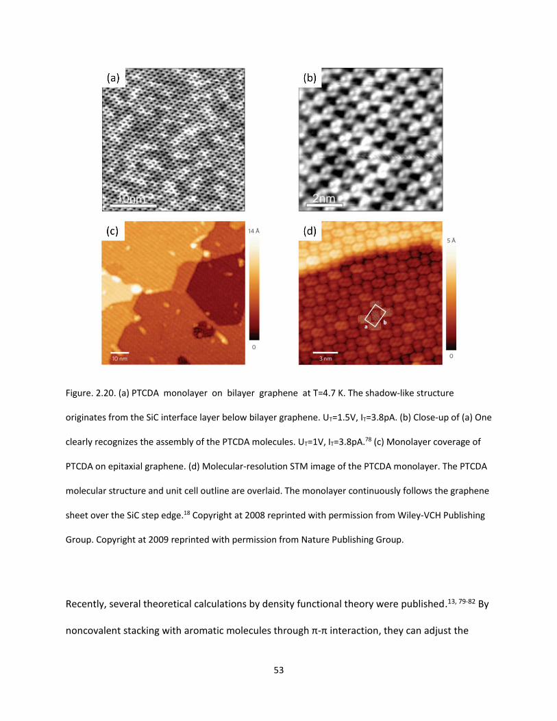
53
Figure. 2.20. (a) PTCDA monolayer on bilayer graphene at T=4.7 K. The shadow-like structure
originates from the SiC interface layer below bilayer graphene. UT=1.5V, IT=3.8pA. (b) Close-up of (a) One
clearly recognizes the assembly of the PTCDA molecules. UT=1V, IT=3.8pA.78 (c) Monolayer coverage of
PTCDA on epitaxial graphene. (d) Molecular-resolution STM image of the PTCDA monolayer. The PTCDA
molecular structure and unit cell outline are overlaid. The monolayer continuously follows the graphene
sheet over the SiC step edge.18 Copyright at 2008 reprinted with permission from Wiley-VCH Publishing
Group. Copyright at 2009 reprinted with permission from Nature Publishing Group.
Recently, several theoretical calculations by density functional theory were published.13, 79-82 By
noncovalent stacking with aromatic molecules through π-π interaction, they can adjust the
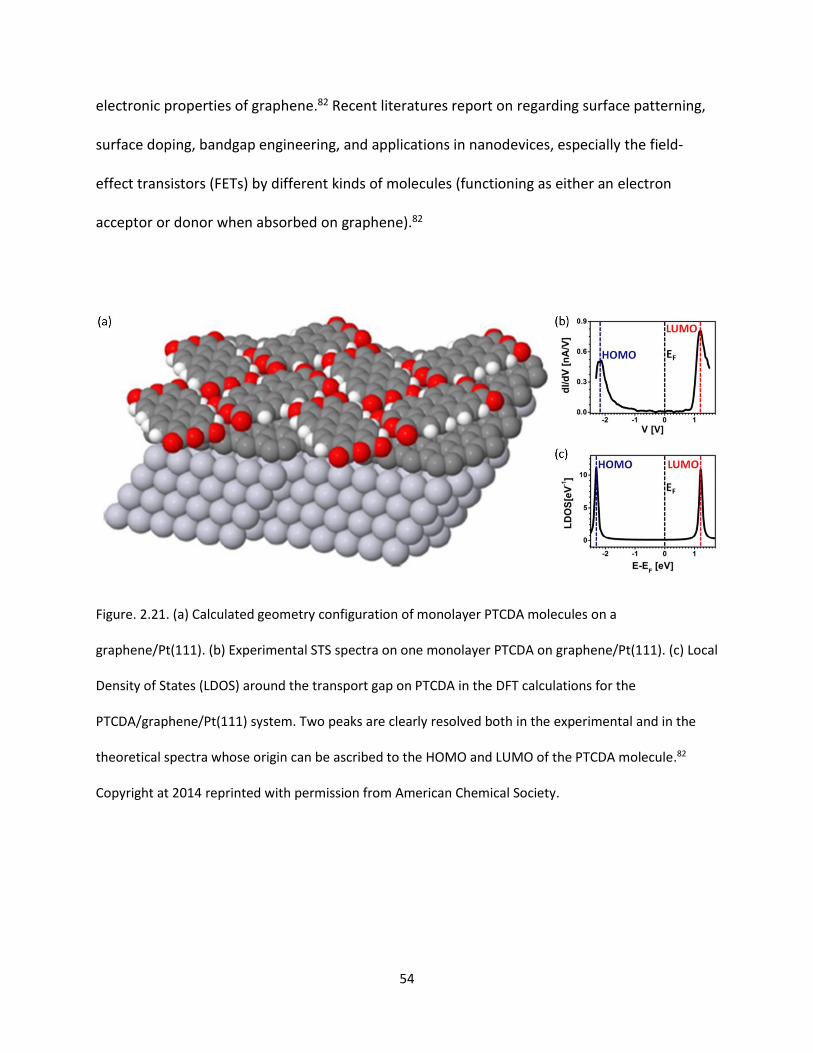
54
electronic properties of graphene.82 Recent literatures report on regarding surface patterning,
surface doping, bandgap engineering, and applications in nanodevices, especially the field-
effect transistors (FETs) by different kinds of molecules (functioning as either an electron
acceptor or donor when absorbed on graphene).82
Figure. 2.21. (a) Calculated geometry configuration of monolayer PTCDA molecules on a
graphene/Pt(111). (b) Experimental STS spectra on one monolayer PTCDA on graphene/Pt(111). (c) Local
Density of States (LDOS) around the transport gap on PTCDA in the DFT calculations for the
PTCDA/graphene/Pt(111) system. Two peaks are clearly resolved both in the experimental and in the
theoretical spectra whose origin can be ascribed to the HOMO and LUMO of the PTCDA molecule.82
Copyright at 2014 reprinted with permission from American Chemical Society.
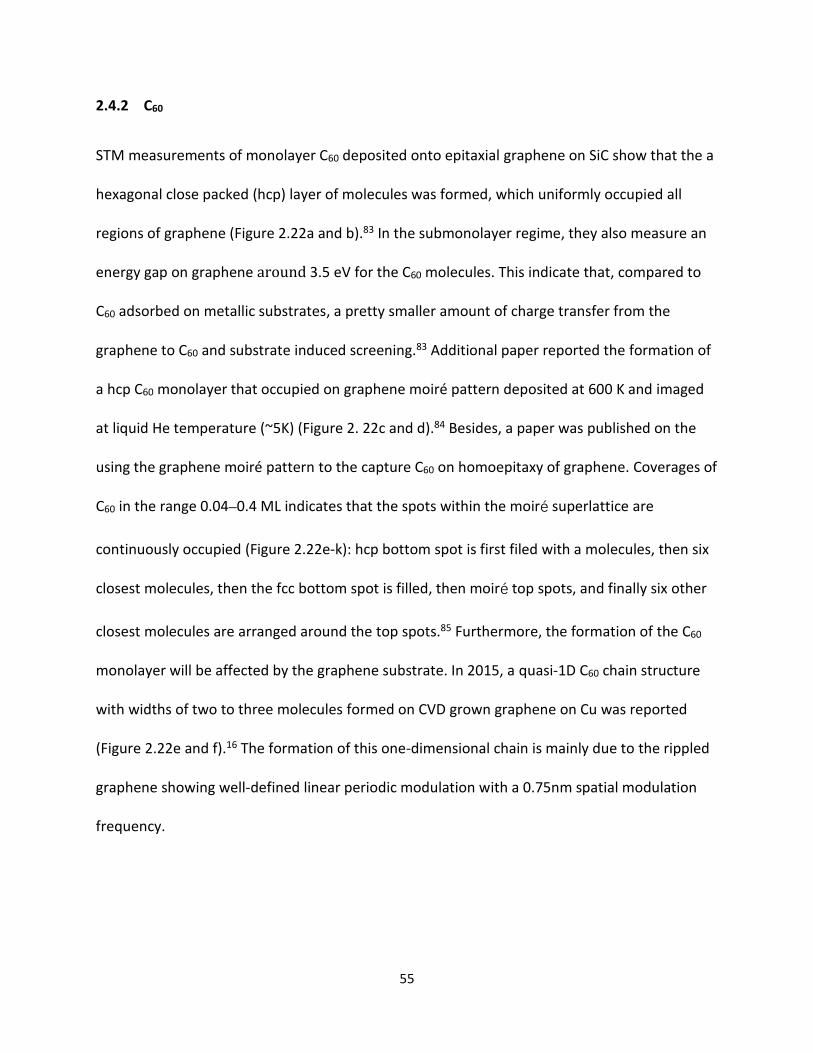
55
2.4.2 C60
STM measurements of monolayer C60 deposited onto epitaxial graphene on SiC show that the a
hexagonal close packed (hcp) layer of molecules was formed, which uniformly occupied all
regions of graphene (Figure 2.22a and b).83 In the submonolayer regime, they also measure an
energy gap on graphene around 3.5 eV for the C60 molecules. This indicate that, compared to
C60 adsorbed on metallic substrates, a pretty smaller amount of charge transfer from the
graphene to C60 and substrate induced screening.83 Additional paper reported the formation of
a hcp C60 monolayer that occupied on graphene moiré pattern deposited at 600 K and imaged
at liquid He temperature (~5K) (Figure 2. 22c and d).84 Besides, a paper was published on the
using the graphene moiré pattern to the capture C60 on homoepitaxy of graphene. Coverages of
C60 in the range 0.04–0.4 ML indicates that the spots within the moiré superlattice are
continuously occupied (Figure 2.22e-k): hcp bottom spot is first filed with a molecules, then six
closest molecules, then the fcc bottom spot is filled, then moiré top spots, and finally six other
closest molecules are arranged around the top spots.85 Furthermore, the formation of the C60
monolayer will be affected by the graphene substrate. In 2015, a quasi-1D C60 chain structure
with widths of two to three molecules formed on CVD grown graphene on Cu was reported
(Figure 2.22e and f).16 The formation of this one-dimensional chain is mainly due to the rippled
graphene showing well-defined linear periodic modulation with a 0.75nm spatial modulation
frequency.
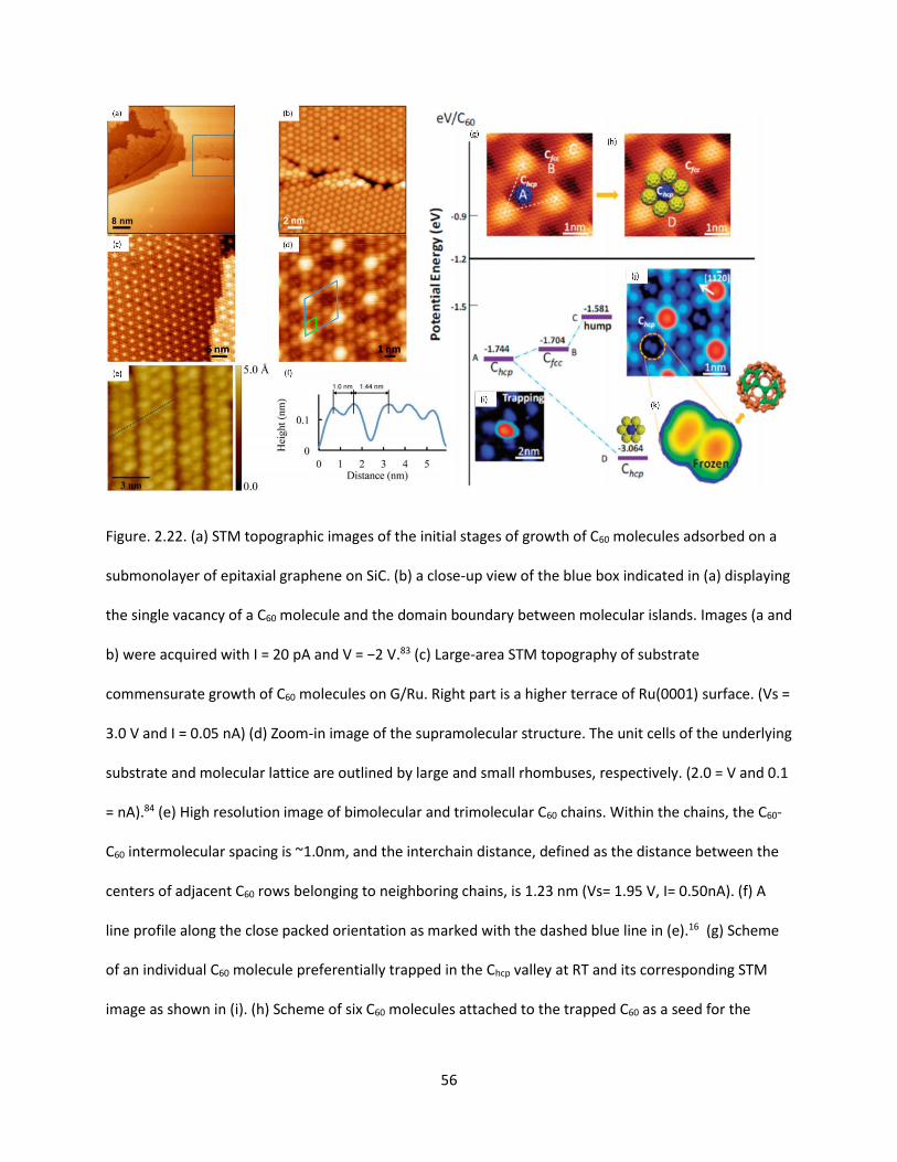
56
Figure. 2.22. (a) STM topographic images of the initial stages of growth of C60 molecules adsorbed on a
submonolayer of epitaxial graphene on SiC. (b) a close-up view of the blue box indicated in (a) displaying
the single vacancy of a C60 molecule and the domain boundary between molecular islands. Images (a and
b) were acquired with I = 20 pA and V = −2 V.83 (c) Large-area STM topography of substrate
commensurate growth of C60 molecules on G/Ru. Right part is a higher terrace of Ru(0001) surface. (Vs =
3.0 V and I = 0.05 nA) (d) Zoom-in image of the supramolecular structure. The unit cells of the underlying
substrate and molecular lattice are outlined by large and small rhombuses, respectively. (2.0 = V and 0.1
= nA).84 (e) High resolution image of bimolecular and trimolecular C60 chains. Within the chains, the C60-
C60 intermolecular spacing is ~1.0nm, and the interchain distance, defined as the distance between the
centers of adjacent C60 rows belonging to neighboring chains, is 1.23 nm (Vs= 1.95 V, I= 0.50nA). (f) A
line profile along the close packed orientation as marked with the dashed blue line in (e).16 (g) Scheme
of an individual C60 molecule preferentially trapped in the Chcp valley at RT and its corresponding STM
image as shown in (i). (h) Scheme of six C60 molecules attached to the trapped C60 as a seed for the
57
nucleation of monolayer C60 islands; C60-C60 cohesive energy increases. (j) RT freezing of the thermal
motions of C60 in the Chcp valleys once a C60 monolayer is formed. (k) All C60 molecules trapped in Chcp
valleys display a dumbbell shape, aligning along the <1120> directions. The bright lobes in the dumbbell-
shaped correspond to pentagons of the C60 cage at positive sample bias, which suggests C60 orients with
the 6:6 bond (the C-C bond between two carbon hexagons) facing upward, as shown in the right top of
(k).85 Copyright at 2012 reprinted with permission from American Chemical Society. Copyright at 2012
reprinted with permission from American Institute of Physics. Copyright at 2015 reprinted with
permission from Nature Publishing Group. Copyright at 2012 reprinted with permission from American
Chemical Society.
2.4.3 Phthalocyanines
Phthalocyanines (shown as unsubstituted phathalocyanine, H2Pc, in Figure 2.19) can be used as
a π‐conjugated organic cell for metal atoms (FePc20, 86-87, CoPc19, F16CoPc19, NiPc, ClAlPc88) fixed
at the center of the molecule. In this style, they are called metal‐pthalocyanines (M‐Pc), and
their spin states and orbital energetics are highly influenced by the type of metal center and by
possible side groups. They lie flat on the surface of HOPG, and lateral stabilization is provided
by the Van der Waals interaction between H‐terminated M‐Pc for their close packed self‐
assembled structure. At low coverage (less than 5%), FePc molecules prefer to be deposited on
the fcc spots of the graphene moiré pattern.20 As coverage increases, they continuing occupy
more fcc regions until an ordered 2D superlattice of separated molecules is formed on the
graphene (Figure 2.23b). Once the fcc regions are all occupied, the remaining FePc tends to stay
at the hcp regions rather than the top regions (Figure 2.23c).20 At a higher coverage (75%), FePc

58
forms a Kagome lattice (consisting of the vertices and edges of the trihexagonal tiling) (Figure
2.23d) with the open networks occupying both the hcp and fcc spots of graphene, with the top
spots whole empty.86 For a fully covered monolayer, all Pc molecules create a square lattice
including FePc, CoPc, ClAlPc and other MPcs (Figure 2.23 f-j).87 In 2011, a DFT group calculated
the optimal density of states (DOS) and configuration of the adsorption system (solid black thick
line), and that projected onto the Pc molecule (solid blue line) and the graphene substrate
(solid black thin line) (Figure 2.23 k and l).89 The two characteristics above and below Fermi
Energy (EF) in the total DOS almost are caused by the contributions of LUMO and HOMO states
of F16CuPc, including, three spin-down and two spin-up orbitals (for LUMOs)and one spin-down
and two spin-up orbital (for HOMOs), respectively.89
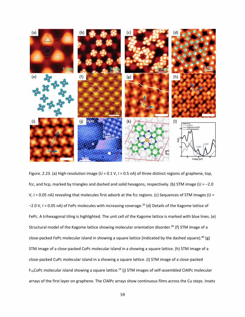
59
Figure. 2.23. (a) High-resolution image (U = 0.1 V, I = 0.5 nA) of three distinct regions of graphene, top,
fcc, and hcp, marked by triangles and dashed and solid hexagons, respectively. (b) STM image (U = −2.0
V, I = 0.05 nA) revealing that molecules first adsorb at the fcc regions. (c) Sequences of STM images (U =
−2.0 V, I = 0.05 nA) of FePc molecules with increasing coverage.20 (d) Details of the Kagome lattice of
FePc. A trihexagonal tiling is highlighted. The unit cell of the Kagome lattice is marked with blue lines. (e)
Structural model of the Kagome lattice showing molecular orientation disorder.85 (f) STM image of a
close-packed FePc molecular island in showing a square lattice (indicated by the dashed square).80 (g)
STM image of a close-packed CoPc molecular island in a showing a square lattice. (h) STM image of a
close-packed CuPc molecular island in a showing a square lattice. (i) STM image of a close-packed
F16CoPc molecular island showing a square lattice.19 (j) STM images of self-assembled ClAlPc molecular
arrays of the first layer on graphene. The ClAlPc arrays show continuous films across the Cu steps. Insets
60
show the magnified images (Vtip = 2.0 V, I = 75 pA).88 (k) The optimized configuration for the
F16CuPc/graphene [(3,4)×(4,3)] system. (l) Total DOS (thick black solid line) and projected DOS on the Pc
molecule (blue solid line), on graphene (thin black solid line), upon F16CuPc adsorption on graphene, and
the DOS of the isolated graphene (black dashed dotted line). The vertical dotted line shows the Fermi
level.89 Copyright at 2011 reprinted with permission from American Physical Society. Copyright at 2009
reprinted with permission from American Chemical Society. Copyright at 2012 reprinted with permission
from American Chemical Society. Copyright at 2013 reprinted with permission from American Chemical
Society. Copyright at 2011 reprinted with permission from American Institute of Physics.
References:
1. Novoselov, K. S.; Geim, A. K.; Morozov, S. V.; Jiang, D.; Zhang, Y.; Dubonos, S. V.; Grigorieva, I. V.; Firsov, A. A., Electric field effect in atomically thin carbon films. Science 2004, 306 (5696), 666-669. 2. Saito, R.; Fujita, M.; Dresselhaus, G.; Dresselhaus, M. S., Electronic-Structure of Chiral Graphene Tubules. Appl Phys Lett 1992, 60 (18), 2204-2206. 3. Allen, M. J.; Tung, V. C.; Kaner, R. B., Honeycomb Carbon: A Review of Graphene. Chem Rev 2010, 110 (1), 132-145. 4. Choi, W.; Lahiri, I.; Seelaboyina, R.; Kang, Y. S., Synthesis of Graphene and Its Applications: A Review. Crit Rev Solid State 2010, 35 (1), 52-71. 5. Ohta, T.; Bostwick, A.; Seyller, T.; Horn, K.; Rotenberg, E., Controlling the electronic structure of bilayer graphene. Science 2006, 313 (5789), 951-954. 6. Lee, H.; Paeng, K.; Kim, I. S., A review of doping modulation in graphene. Synthetic Met 2018, 244, 36-47. 7. Zhao, J.; Zhang, G. Y.; Shi, D. X., Review of graphene-based strain sensors. Chinese Phys B 2013, 22 (5). 8. Dutta, S.; Pati, S. K., Novel properties of graphene nanoribbons: a review. J Mater Chem 2010, 20 (38), 8207-8223. 9. MacLeod, J. M.; Rosei, F., Molecular Self-Assembly on Graphene. Small 2014, 10 (6), 1038-1049. 10. Munoz, R.; Gomez-Aleixandre, C., Review of CVD Synthesis of Graphene. Chem Vapor Depos 2013, 19 (10-12), 297-322. 11. Akinwande, D.; Brennan, C. J.; Bunch, J. S.; Egberts, P.; Felts, J. R.; Gao, H. J.; Huang, R.; Kim, J. S.; Li, T.; Li, Y.; Liechti, K. M.; Lu, N. S.; Park, H. S.; Reed, E. J.; Wang, P.; Yakobson, B. I.; Zhang, T.; Zhang, Y. W.; Zhou, Y.; Zhu, Y., A review on mechanics and mechanical properties of 2D materials-Graphene and beyond. Extreme Mech Lett 2017, 13, 42-77. 12. Clair, S.; Pons, S.; Fabris, S.; Baroni, S.; Brune, H.; Kern, K.; Barth, J. V., Monitoring two-dimensional coordination reactions: Directed assembly of Co-terephthalate nanosystems on Au(111). J Phys Chem B 2006, 110 (11), 5627-5632.
61
13. Lackinger, M.; Heckl, W. M., Carboxylic Acids: Versatile Building Blocks and Mediators for Two-Dimensional Supramolecular Self-Assembly. Langmuir 2009, 25 (19), 11307-11321. 14. Altman, E. I.; Colton, R. J., Determination of the Orientation of C-60 Adsorbed on Au(111) and Ag(111). Phys Rev B 1993, 48 (24), 18244-18249. 15. Cheng, F.; Wu, X. J.; Hu, Z. X.; Lu, X. F.; Ding, Z. J.; Shao, Y.; Xu, H.; Ji, W.; Wu, J. S.; Loh, K. P., Two-dimensional tessellation by molecular tiles constructed from halogen-halogen and halogen-metal networks. Nat Commun 2018, 9. 16. Chen, C. H.; Zheng, H. S.; Mills, A.; Heflin, J. R.; Tao, C. G., Temperature Evolution of Quasi-one-dimensional C-60 Nanostructures on Rippled Graphene. Sci Rep-Uk 2015, 5. 17. Meissner, M.; Gruenewald, M.; Sojka, F.; Udhardt, C.; Forker, R.; Fritz, T., Highly ordered growth of PTCDA on epitaxial bilayer graphene. Surf Sci 2012, 606 (21-22), 1709-1715. 18. Wang, Q. H.; Hersam, M. C., Room-temperature molecular-resolution characterization of self-assembled organic monolayers on epitaxial graphene. Nat Chem 2009, 1 (3), 206-211. 19. Jarvinen, P.; Hamalainen, S. K.; Ijas, M.; Harju, A.; Liljeroth, P., Self-Assembly and Orbital Imaging of Metal Phthalocyanines on a Graphene Model Surface. J Phys Chem C 2014, 118 (24), 13320-13325. 20. Zhang, H. G.; Sun, J. T.; Low, T.; Zhang, L. Z.; Pan, Y.; Liu, Q.; Mao, J. H.; Zhou, H. T.; Guo, H. M.; Du, S. X.; Guinea, F.; Gao, H. J., Assembly of iron phthalocyanine and pentacene molecules on a graphene monolayer grown on Ru(0001). Phys Rev B 2011, 84 (24). 21. Kuzmenko, A. B.; van Heumen, E.; Carbone, F.; van der Marel, D., Universal optical conductance of graphite. Phys Rev Lett 2008, 100 (11). 22. Geim, A. K.; Novoselov, K. S., The rise of graphene. Nat Mater 2007, 6 (3), 183-191. 23. Huang, Y.; Sutter, E.; Shi, N. N.; Zheng, J. B.; Yang, T. Z.; Englund, D.; Gao, H. J.; Sutter, P., Reliable Exfoliation of Large-Area High-Quality Flakes of Graphene and Other Two-Dimensional Materials. Acs Nano 2015, 9 (11), 10612-10620. 24. Sutter, P. W.; Flege, J. I.; Sutter, E. A., Epitaxial graphene on ruthenium. Nat Mater 2008, 7 (5), 406-411. 25. Yang, W.; Chen, G. R.; Shi, Z. W.; Liu, C. C.; Zhang, L. C.; Xie, G. B.; Cheng, M.; Wang, D. M.; Yang, R.; Shi, D. X.; Watanabe, K.; Taniguchi, T.; Yao, Y. G.; Zhang, Y. B.; Zhang, G. Y., Epitaxial growth of single-domain graphene on hexagonal boron nitride. Nat Mater 2013, 12 (9), 792-797. 26. Berger, C.; Song, Z. M.; Li, T. B.; Li, X. B.; Ogbazghi, A. Y.; Feng, R.; Dai, Z. T.; Marchenkov, A. N.; Conrad, E. H.; First, P. N.; de Heer, W. A., Ultrathin epitaxial graphite: 2D electron gas properties and a route toward graphene-based nanoelectronics. J Phys Chem B 2004, 108 (52), 19912-19916. 27. Kim, K. S.; Zhao, Y.; Jang, H.; Lee, S. Y.; Kim, J. M.; Kim, K. S.; Ahn, J. H.; Kim, P.; Choi, J. Y.; Hong, B. H., Large-scale pattern growth of graphene films for stretchable transparent electrodes. Nature 2009, 457 (7230), 706-710. 28. Reina, A.; Jia, X. T.; Ho, J.; Nezich, D.; Son, H. B.; Bulovic, V.; Dresselhaus, M. S.; Kong, J., Large Area, Few-Layer Graphene Films on Arbitrary Substrates by Chemical Vapor Deposition. Nano Lett 2009, 9 (1), 30-35. 29. Nair, R. R.; Blake, P.; Grigorenko, A. N.; Novoselov, K. S.; Booth, T. J.; Stauber, T.; Peres, N. M. R.; Geim, A. K., Fine structure constant defines visual transparency of graphene. Science 2008, 320 (5881), 1308-1308. 30. Meric, I.; Han, M. Y.; Young, A. F.; Ozyilmaz, B.; Kim, P.; Shepard, K. L., Current saturation in zero-bandgap, topgated graphene field-effect transistors. Nat Nanotechnol 2008, 3 (11), 654-659. 31. Novoselov, K. S.; Jiang, D.; Schedin, F.; Booth, T. J.; Khotkevich, V. V.; Morozov, S. V.; Geim, A. K., Two-dimensional atomic crystals. P Natl Acad Sci USA 2005, 102 (30), 10451-10453. 32. Datta, S. S.; Strachan, D. R.; Khamis, S. M.; Johnson, A. T. C., Crystallographic etching of few-layer graphene. Nano Lett 2008, 8 (7), 1912-1915.
62
33. Gass, M. H.; Bangert, U.; Bleloch, A. L.; Wang, P.; Nair, R. R.; Geim, A. K., Free-standing graphene at atomic resolution. Nat Nanotechnol 2008, 3 (11), 676-681. 34. Huc, V.; Bendiab, N.; Rosman, N.; Ebbesen, T.; Delacour, C.; Bouchiat, V., Large and flat graphene flakes produced by epoxy bonding and reverse exfoliation of highly oriented pyrolytic graphite. Nanotechnology 2008, 19 (45). 35. Li, X. S.; Cai, W. W.; An, J. H.; Kim, S.; Nah, J.; Yang, D. X.; Piner, R.; Velamakanni, A.; Jung, I.; Tutuc, E.; Banerjee, S. K.; Colombo, L.; Ruoff, R. S., Large-Area Synthesis of High-Quality and Uniform Graphene Films on Copper Foils. Science 2009, 324 (5932), 1312-1314. 36. Edwards, R. S.; Coleman, K. S., Graphene Film Growth on Polycrystalline Metals. Accounts Chem Res 2013, 46 (1), 23-30. 37. Castro Neto, A. H.; Guinea, F.; Peres, N. M. R.; Novoselov, K. S.; Geim, A. K., The electronic properties of graphene. Rev Mod Phys 2009, 81 (1), 109-162. 38. Pan, Y.; Shi, D. X.; Gao, H. J., Formation of graphene on Ru(0001) surface. Chinese Phys 2007, 16 (11), 3151-3153. 39. Gottardi, S.; Muller, K.; Bignardi, L.; Moreno-Lopez, J. C.; Pham, T. A.; Ivashenko, O.; Yablonskikh, M.; Barinov, A.; Bjork, J.; Rudolf, P.; Stohr, M., Comparing Graphene Growth on Cu(111) versus Oxidized Cu(111). Nano Lett 2015, 15 (2), 917-922. 40. Tapaszto, L.; Dumitrica, T.; Kim, S. J.; Nemes-Incze, P.; Hwang, C.; Biro, L. P., Breakdown of continuum mechanics for nanometre-wavelength rippling of graphene. Nat Phys 2012, 8 (10), 739-742. 41. Zhu, Y. W.; Murali, S.; Cai, W. W.; Li, X. S.; Suk, J. W.; Potts, J. R.; Ruoff, R. S., Graphene and Graphene Oxide: Synthesis, Properties, and Applications. Adv Mater 2010, 22 (35), 3906-3924. 42. Novoselov, K. S.; Geim, A. K.; Morozov, S. V.; Jiang, D.; Katsnelson, M. I.; Grigorieva, I. V.; Dubonos, S. V.; Firsov, A. A., Two-dimensional gas of massless Dirac fermions in graphene. Nature 2005, 438 (7065), 197-200. 43. Bolotin, K. I.; Sikes, K. J.; Jiang, Z.; Klima, M.; Fudenberg, G.; Hone, J.; Kim, P.; Stormer, H. L., Ultrahigh electron mobility in suspended graphene. Solid State Commun 2008, 146 (9-10), 351-355. 44. Frank, I. W.; Tanenbaum, D. M.; Van der Zande, A. M.; McEuen, P. L., Mechanical properties of suspended graphene sheets. J Vac Sci Technol B 2007, 25 (6), 2558-2561. 45. Poot, M.; van der Zant, H. S. J., Nanomechanical properties of few-layer graphene membranes. Appl Phys Lett 2008, 92 (6). 46. Lee, C.; Wei, X. D.; Kysar, J. W.; Hone, J., Measurement of the elastic properties and intrinsic strength of monolayer graphene. Science 2008, 321 (5887), 385-388. 47. Gomez-Navarro, C.; Burghard, M.; Kern, K., Elastic properties of chemically derived single graphene sheets. Nano Lett 2008, 8 (7), 2045-2049. 48. Ni, Z. H.; Wang, H. M.; Kasim, J.; Fan, H. M.; Yu, T.; Wu, Y. H.; Feng, Y. P.; Shen, Z. X., Graphene thickness determination using reflection and contrast spectroscopy. Nano Lett 2007, 7 (9), 2758-2763. 49. Peres, N. M. R.; Guinea, F.; Castro Neto, A. H., Electronic properties of disordered two-dimensional carbon. Phys Rev B 2006, 73 (12). 50. Gusynin, V. P.; Sharapov, S. G.; Carbotte, J. P., Unusual microwave response of Dirac quasiparticles in graphene. Phys Rev Lett 2006, 96 (25). 51. Peres, N. M. R., The transport properties of graphene. J Phys-Condens Mat 2009, 21 (32). 52. Cao, Y.; Fatemi, V.; Fang, S.; Watanabe, K.; Taniguchi, T.; Kaxiras, E.; Jarillo-Herrero, P., Unconventional superconductivity in magic-angle graphene superlattices. Nature 2018, 556 (7699), 43-+. 53. Cao, Y.; Fatemi, V.; Demir, A.; Fang, S.; Tomarken, S. L.; Luo, J. Y.; Sanchez-Yamagishi, J. D.; Watanabe, K.; Taniguchi, T.; Kaxiras, E.; Ashoori, R. C.; Jarillo-Herrero, P., Correlated insulator behaviour at half-filling in magic-angle graphene superlattices. Nature 2018, 556 (7699), 80-+.
63
54. Chen, G. R.; Jiang, L. L.; Wu, S.; Lyu, B.; Li, H. Y.; Chittari, B. L.; Watanabe, K.; Taniguchi, T.; Shi, Z. W.; Jung, J.; Zhang, Y. B.; Wang, F., Evidence of a gate-tunable Mott insulator in a trilayer graphene moire superlattice. Nat Phys 2019, 15 (3), 237-241. 55. Wu, Z. S.; Pei, S. F.; Ren, W. C.; Tang, D. M.; Gao, L. B.; Liu, B. L.; Li, F.; Liu, C.; Cheng, H. M., Field Emission of Single-Layer Graphene Films Prepared by Electrophoretic Deposition. Adv Mater 2009, 21 (17), 1756-+. 56. Shao, Y. Y.; Wang, J.; Wu, H.; Liu, J.; Aksay, I. A.; Lin, Y. H., Graphene Based Electrochemical Sensors and Biosensors: A Review. Electroanal 2010, 22 (10), 1027-1036. 57. Yoon, H. J.; Jun, D. H.; Yang, J. H.; Zhou, Z. X.; Yang, S. S.; Cheng, M. M. C., Carbon dioxide gas sensor using a graphene sheet. Sensor Actuat B-Chem 2011, 157 (1), 310-313. 58. De Arco, L. G.; Zhang, Y.; Schlenker, C. W.; Ryu, K.; Thompson, M. E.; Zhou, C. W., Continuous, Highly Flexible, and Transparent Graphene Films by Chemical Vapor Deposition for Organic Photovoltaics. Acs Nano 2010, 4 (5), 2865-2873. 59. Yoo, E.; Kim, J.; Hosono, E.; Zhou, H.; Kudo, T.; Honma, I., Large reversible Li storage of graphene nanosheet families for use in rechargeable lithium ion batteries. Nano Lett 2008, 8 (8), 2277-2282. 60. Bigelow, W. C.; Pickett, D. L.; Zisman, W. A., Oleophobic Monolayers .1. Films Adsorbed from Solution in Non-Polar Liquids. J Coll Sci Imp U Tok 1946, 1 (6), 513-538. 61. Gast, A. P., Physical chemistry of surfaces. New York, A Wiley-Interscience Publication 1997. 62. Love, J. C.; Estroff, L. A.; Kriebel, J. K.; Nuzzo, R. G.; Whitesides, G. M., Self-assembled monolayers of thiolates on metals as a form of nanotechnology. Chem Rev 2005, 105 (4), 1103-1169. 63. Nuzzo, R. G.; Allara, D. L., Adsorption of Bifunctional Organic Disulfides on Gold Surfaces. J Am Chem Soc 1983, 105 (13), 4481-4483. 64. Maoz, R.; Sagiv, J., On the Formation and Structure of Self-Assembling Monolayers .1. A Comparative Atr-Wetability Study of Langmuir-Blodgett and Adsorbed Films on Flat Substrates and Glass Microbeads. J Colloid Interf Sci 1984, 100 (2), 465-496. 65. Lehn, J. M., Supramolecular Chemistry-Concepts and Chemistry. VCH: Wiley: Weinheim 1995. 66. Elemans, J. A. A. W.; Lei, S. B.; De Feyter, S., Molecular and Supramolecular Networks on Surfaces: From Two-Dimensional Crystal Engineering to Reactivity. Angew Chem Int Edit 2009, 48 (40), 7298-7332. 67. Binning, G.; Rohrer, H.; Gerber, C.; Weibel, E., Surface Studies by Scanning Tunneling Microscopy. Phys Rev Lett 1982, 49 (1), 57-61. 68. Barth, J. V., Fresh perspectives for surface coordination chemistry. Surf Sci 2009, 603 (10-12), 1533-1541. 69. Ivasenko, O.; Perepichka, D. F., Mastering fundamentals of supramolecular design with carboxylic acids. Common lessons from X-ray crystallography and scanning tunneling microscopy. Chem Soc Rev 2011, 40 (1), 191-206. 70. https://en.wikipedia.org/wiki?curid=13609. 71. C. Nörenberg, D. F. L., D. Cattaneo, K. Porfyrakis, A. Li Bassi, C.S. Casari, M. Passoni, J.H.G. Owen, G.A.D. Briggs, Self-assembly and electronic effects of Er3N@C80 and Sc3N@C80 on Au(111) and Ag/Si(111) surfaces. J. Phys. Conf. Ser. 2008, 100, 052080. 72. https://en.wikipedia.org/wiki/Van_der_Waals_force. 73. https://en.wikipedia.org/wiki?curid=14350687. 74. Gutzler, R.; Ivasenko, O.; Fu, C. Y.; Brusso, J. L.; Rosei, F.; Perepichka, D. F., Halogen bonds as stabilizing interactions in a chiral self-assembled molecular monolayer. Chem Commun 2011, 47 (33), 9453-9455. 75. Gutzler, R.; Fu, C. Y.; Dadvand, A.; Hua, Y.; MacLeod, J. M.; Rosei, F.; Perepichka, D. F., Halogen bonds in 2D supramolecular self-assembly of organic semiconductors. Nanoscale 2012, 4 (19), 5965-5971.
64
76. Bonifazi, D.; Mohnani, S.; Llanes-Pallas, A., Supramolecular Chemistry at Interfaces: Molecular Recognition on Nanopatterned Porous Surfaces. Chem-Eur J 2009, 15 (29), 7004-7025. 77. De Feyter, S.; De Schryver, F. C., Two-dimensional supramolecular self-assembly probed by scanning tunneling microscopy (vol 32, pg 139, 2003). Chem Soc Rev 2003, 32 (6), 393-393. 78. Lauffer, P.; Emtsev, K. V.; Graupner, R.; Seyller, T.; Ley, L., Molecular and electronic structure of PTCDA on bilayer graphene on SiC(0001) studied with scanning tunneling microscopy. Phys Status Solidi B 2008, 245 (10), 2064-2067. 79. Tian, X. Q.; Xu, J. B.; Wang, X. M., Self-Assembly of PTCDA Ultrathin Films on Graphene: Structural Phase Transition and Charge Transfer Saturation. J Phys Chem C 2010, 114 (49), 20917-20924. 80. Kozlov, S. M.; Vines, F.; Gorling, A., Bandgap Engineering of Graphene by Physisorbed Adsorbates. Adv Mater 2011, 23 (22-23), 2638-+. 81. Zhang, Z. X.; Huang, H. L.; Yang, X. M.; Zang, L., Tailoring Electronic Properties of Graphene by pi-pi Stacking with Aromatic Molecules. J Phys Chem Lett 2011, 2 (22), 2897-2905. 82. Martinez-Galera, A. J.; Nicoara, N.; Martinez, J. I.; Dappe, Y. J.; Ortega, J.; Gomez-Rodriguez, J. M., Imaging Molecular Orbitals of PTCDA on Graphene on Pt(111): Electronic Structure by STM and First-Principles Calculations. J Phys Chem C 2014, 118 (24), 12782-12788. 83. Cho, J.; Smerdon, J.; Gao, L.; Suzer, O.; Guest, J. R.; Guisinger, N. P., Structural and Electronic Decoupling of C-60 from Epitaxial Graphene on SiC. Nano Lett 2012, 12 (6), 3018-3024. 84. Li, G.; Zhou, H. T.; Pan, L. D.; Zhang, Y.; Mao, J. H.; Zou, Q.; Guo, H. M.; Wang, Y. L.; Du, S. X.; Gao, H. J., Self-assembly of C-60 monolayer on epitaxially grown, nanostructured graphene on Ru(0001) surface. Appl Phys Lett 2012, 100 (1). 85. Lu, J.; Yeo, P. S. E.; Zheng, Y.; Yang, Z. Y.; Bao, Q. L.; Gan, C. K.; Loh, K. P., Using the Graphene Moire Pattern for the Trapping of C-60 and Homoepitaxy of Graphene. Acs Nano 2012, 6 (1), 944-950. 86. Mao, J. H.; Zhang, H. G.; Jiang, Y. H.; Pan, Y.; Gao, M.; Xiao, W. D.; Gao, H. J., Tunability of Supramolecular Kagome Lattices of Magnetic Phthalocyanines Using Graphene-Based Moire Patterns as Templates. J Am Chem Soc 2009, 131 (40), 14136-+. 87. Yang, K.; Xiao, W. D.; Jiang, Y. H.; Zhang, H. G.; Liu, L. W.; Mao, J. H.; Zhou, H. T.; Du, S. X.; Gao, H. J., Molecule-Substrate Coupling between Metal Phthalocyanines and Epitaxial Graphene Grown on Ru(0001) and Pt(111). J Phys Chem C 2012, 116 (26), 14052-14056. 88. Ogawa, Y.; Niu, T. C.; Wong, S. L.; Tsuji, M.; Wee, A. T. S.; Chen, W.; Ago, H., Self-Assembly of Polar Phthalocyanine Molecules on Graphene Grown by Chemical Vapor Deposition. J Phys Chem C 2013, 117 (42), 21849-21855. 89. Ren, J.; Meng, S.; Wang, Y. L.; Ma, X. C.; Xue, Q. K.; Kaxiras, E., Properties of copper (fluoro-)phthalocyanine layers deposited on epitaxial graphene. J Chem Phys 2011, 134 (19).
65
Chapter 3
Experimental methods
For the purpose of characterizing the morphology of molecules, atoms and hybrid structures at
the nanoscale, a tool with super-high resolution is absolutely essential to observe and record
the nanostructure. As we have already introduced in Chapter 1, all these hybrid structures are
typically at atomic scale, so this experimental tool should have the resolution of at least a
nanometer. Second of all, the structure should not be distorted or damaged during the
measuring process. Scanning tunneling microscopy (STM) and atomic force microscopy (AFM)
are ideally suited due to their capability of atomic resolution and weak interaction compared to
other measurement tools. An ultrahigh vacuum (UHV) STM1® STM from Omicron
Nanotechnology is one of our main instrument used in this thesis, and all the measurements
were done under a base pressure of 1 × 10⁻¹⁰ Torr. A Dimension Icon® AFM from Bruker is the
other equipment that we use during the experiments.
In this chapter, our main tools – STM and AFM will be introduced, including a brief history
development and the fundamental physical mechanism of them. Then we will show the main
designs for the Omicron STM and Bruker ‘Dimension Icon’ AFM in our lab. Finally, we will
explain the other important parts (sample preparation) employed in our experiments, including
the spin coating method and physical vapor deposition method.
66
3.1 Introduction to Atomic Force Microscope (AFM)
After the invention of STM in 1981, the AFM was invented by G. Binning and Ch. Gerber in
1986.1 Since the emergence of commercially available equipment by the end of that 1980s,
AFM has been an important tool for materials, biological and surface research.2-4 AFM exists in
the core facilities of most research universities and in many single researcher laboratories, and
is a standard feature of large corporation research laboratories.5 The AFM is an imaging device
to see the morphology of a surface in three-dimensions (3D) that relies on the atomic force
(Van der Waals forces) between a sharp tip, which has an average diameter of a few
nanometers, and the scanned sample. AFM can image most materials (soft or hard, natural or
synthetic, including biological materials such as biomolecules and cells) regardless of
conductivity or opaqueness. The sample is not only operated in air, but also in liquid
environments, as well as under vacuum. It owns good resolution on the order of 10-9 m, 1000
times higher than the optical microscope. Additionally, overall the scanning efficiency of the
AFM is much higher than STM even though their scanning speed is comparable, because of the
convenience of loading a new sample and AFM tips compared to the time-consuming process
of transferring samples or installing tips during the STM measurement. Therefore, it is a good
supplement for STM during our lab experiments, especially in certain cases, such as a polymer
or insulator surface.
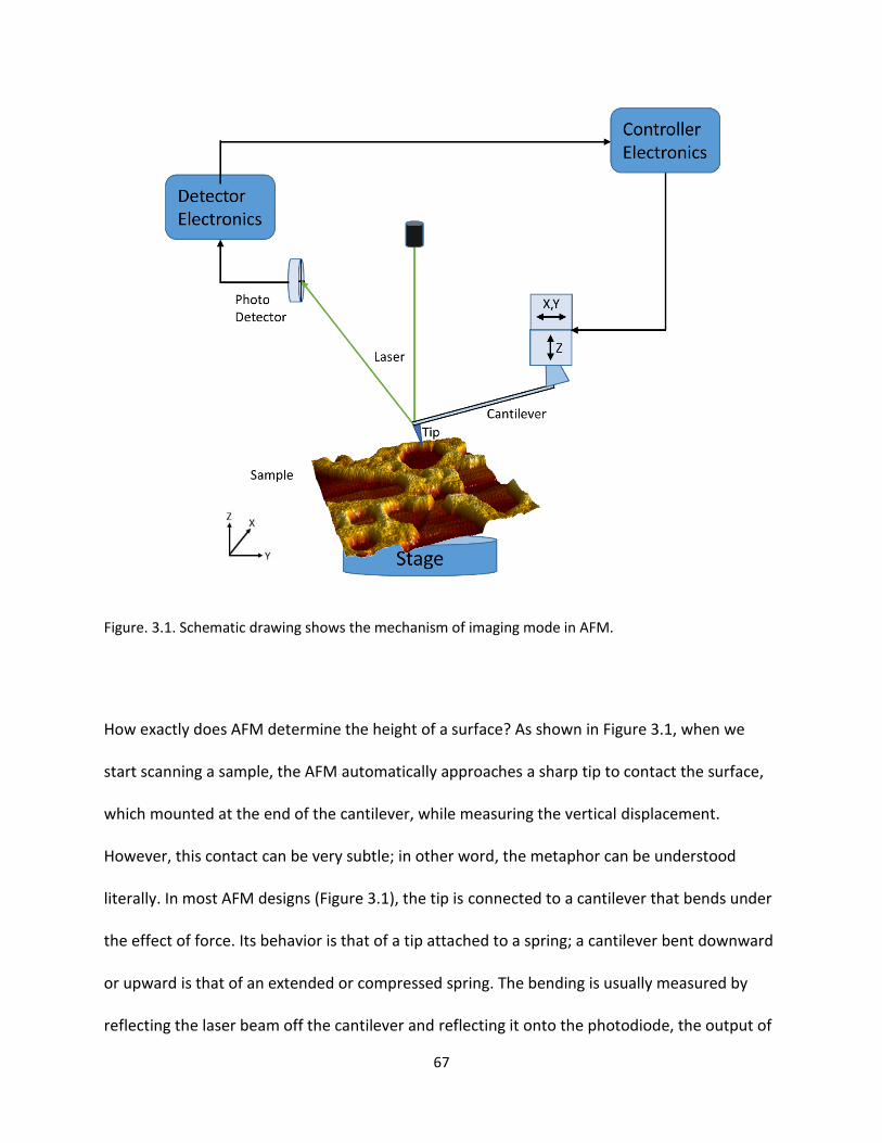
67
Figure. 3.1. Schematic drawing shows the mechanism of imaging mode in AFM.
How exactly does AFM determine the height of a surface? As shown in Figure 3.1, when we
start scanning a sample, the AFM automatically approaches a sharp tip to contact the surface,
which mounted at the end of the cantilever, while measuring the vertical displacement.
However, this contact can be very subtle; in other word, the metaphor can be understood
literally. In most AFM designs (Figure 3.1), the tip is connected to a cantilever that bends under
the effect of force. Its behavior is that of a tip attached to a spring; a cantilever bent downward
or upward is that of an extended or compressed spring. The bending is usually measured by
reflecting the laser beam off the cantilever and reflecting it onto the photodiode, the output of
68
the photodiode measures the position of the laser spot. The vertical movement of the tip is
used to measured this cantilever bending, while the horizontal movement of the laser spot is
used to measure the lateral force that torque the tip. A vertical tip will be usually handled
during the measurement with subnanometer resolution on the order of hundreds of
nanometers. The deflection of the laser will be transformed to electrical information and will be
input to a feedback loop in the controller electronics. The atomic force will keep at a constant
value between tip and sample by a Z direction piezoelectric through this feedback loop. The Z
information of the Z piezo will be recorded as the Z information of the sample, as well as the X
and Y information. In the simplest way, the tip will be brought into contact with a surface,
started to move or scan laterally, and the vertical movement of the tip is measured as the
cantilever bents up and down to measure the surface height, while the tip is sliding on the
surface. By doing so, a surface topography image can established on a 2D grid of locations
across the surface: height versus X and Y, using a pseudocolor key.
3.1.1 Working Principle: Van der Waals Force
Typically, AFM system are operated in three modes: (i) contact mode, (ii), non-contact mode
and (iii) tapping mode. The non-contact mode is utilized to probe atomic forces of a sample by
moving the cantilever slightly off the surface of the sample and having the cantilever near its
resonance frequency or near its natural vibration frequency.6 In non-contact mode,
topographical information of the sample can be extracted by mounting the cantilever on a
piezoelectric element and measuring the deviation from its resonance frequency due to
69
attraction between tip and sample.7 While, the image of the sample is acquired in contact
mode contributing to monitor the interaction forces with the target sample with the cantilever
tip remaining in contact.8 By oscillating the cantilever tip at or near its intrinsic resonance
frequency while reducing the time of impact by cantilever tip on sample to the shortest, the
qualities of both the non-contact and contact modes is combined in tapping mode .9-10
In order to perform nanocharacterization, we need an atomic force or atomic phenomenon
that works in the nanoscale range. The mechanism of imaging in AFM is due to the Van der
Waals interaction between the tip end and sample. The van der Waals force is a distance-
dependent force between molecules or atoms in nanoscale physics, named after scientist
Johannes Diderik van der Waals, and can be described as shown in Figure 3.2 (the force-
displacement curve). These attractive forces, unlike covalent or ionic bonds, are not caused by a
chemical electronic bond; they are relatively weak, and so more impacted by disturbance. The
Van der Waals force dramatically decrease at longer distance between interacting molecules or
atoms. The attraction increases until the molecules are so close that the repulsion appear due
to electrostatic interaction between dipoles or multipoles. As the intermolecular distance
decreasing, this repulsion between the atoms progressively weaken the attraction. When the
distance between the molecules is a few angstroms, the interaction force becomes zero and
then becomes completely repulsive as the molecules are in contact.
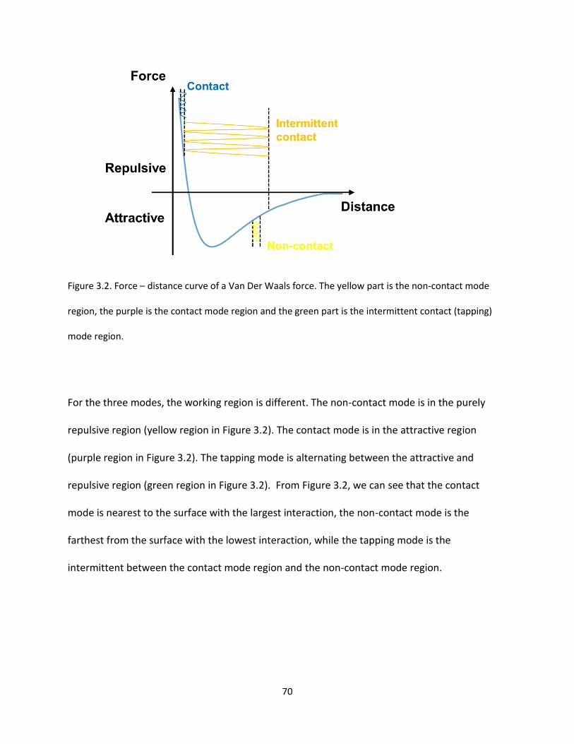
70
Figure 3.2. Force – distance curve of a Van Der Waals force. The yellow part is the non-contact mode
region, the purple is the contact mode region and the green part is the intermittent contact (tapping)
mode region.
For the three modes, the working region is different. The non-contact mode is in the purely
repulsive region (yellow region in Figure 3.2). The contact mode is in the attractive region
(purple region in Figure 3.2). The tapping mode is alternating between the attractive and
repulsive region (green region in Figure 3.2). From Figure 3.2, we can see that the contact
mode is nearest to the surface with the largest interaction, the non-contact mode is the
farthest from the surface with the lowest interaction, while the tapping mode is the
intermittent between the contact mode region and the non-contact mode region.
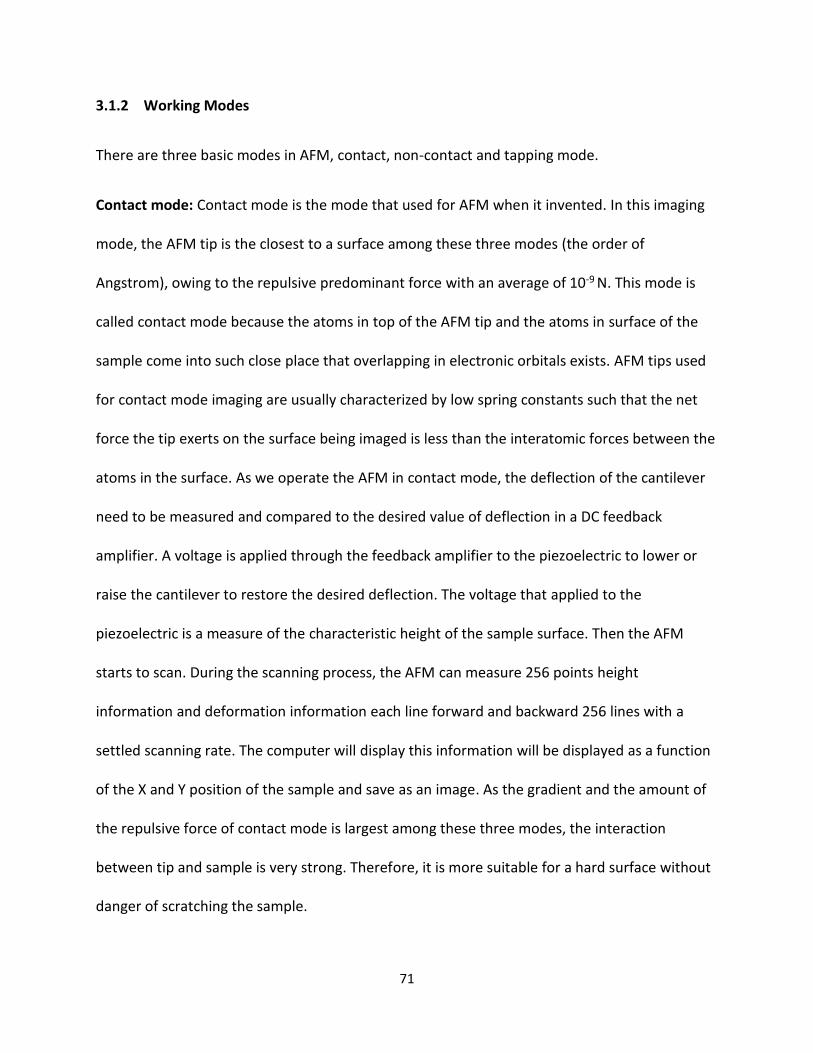
71
3.1.2 Working Modes
There are three basic modes in AFM, contact, non-contact and tapping mode.
Contact mode: Contact mode is the mode that used for AFM when it invented. In this imaging
mode, the AFM tip is the closest to a surface among these three modes (the order of
Angstrom), owing to the repulsive predominant force with an average of 10-9 N. This mode is
called contact mode because the atoms in top of the AFM tip and the atoms in surface of the
sample come into such close place that overlapping in electronic orbitals exists. AFM tips used
for contact mode imaging are usually characterized by low spring constants such that the net
force the tip exerts on the surface being imaged is less than the interatomic forces between the
atoms in the surface. As we operate the AFM in contact mode, the deflection of the cantilever
need to be measured and compared to the desired value of deflection in a DC feedback
amplifier. A voltage is applied through the feedback amplifier to the piezoelectric to lower or
raise the cantilever to restore the desired deflection. The voltage that applied to the
piezoelectric is a measure of the characteristic height of the sample surface. Then the AFM
starts to scan. During the scanning process, the AFM can measure 256 points height
information and deformation information each line forward and backward 256 lines with a
settled scanning rate. The computer will display this information will be displayed as a function
of the X and Y position of the sample and save as an image. As the gradient and the amount of
the repulsive force of contact mode is largest among these three modes, the interaction
between tip and sample is very strong. Therefore, it is more suitable for a hard surface without
danger of scratching the sample.
72
Figure 3.3. (a) The schematic drawing of contact mode. (b) The schematic drawing of non-contact mode.
(c) The schematic drawing of tapping mode.11
Non-contact mode: Since the invention of AFM, although contact mode cannot achieve atomic
resolution stably, it has successfully obtained a number of excellent results at nanoscales level
or even the atomic level through simple contact measurements. In 1994 F.J. Giessibl
successfully obtained atomic resolution AFM images of the Si(111)-(77) surface by a non-
contact AFM by utilizing a frequency modulation detection method under a weak tip-sample
attraction at room temperature in UHV.12 Soon the non-contact mode successfully
accomplished atomically resolved images on various surfaces.13-15 Non-contact mode depends
73
on oscillating the tip near its resonant frequency. In this mode, the separation between tip and
surface of the sample is larger than it is in contact mode, while smaller than tapping mode. The
tip – sample separation is this mode is between tens to hundreds of Angstroms. The oscillation
amplitudes are a bit smaller than this. In this mode, the smallest separation between the tip
and the surface is larger than the smallest separation for both contact and tapping modes. A
strong interaction can be prevented between the tip and the surface by keeping the distance
relatively large between them. In this imaging mode, the system simultaneously monitors the
amplitude as well as the frequency of oscillation of the tip. Any changes in either the amplitude
or the frequency are used through the feedback system to control the piezoelectric scanner in
the Z direction as to minimize these changes and maintain the original amplitude and frequency
of oscillation. This keeps the separation between tip and surface constant, and the profile of
how the tip was moved to keep this constant separation yields the height profile of the sample.
Tapping mode: The technique of tapping mode is an important improvement in AFM. It is
another mode of imaging that depends on oscillating the tip near its resonant frequency, which
firstly was used in biological surfaces field in 1993.16 In tapping mode, the AFM tip is oscillated at
or near its resonant frequency at an optimum amplitude. The tips used for this mode of imaging
are characterized with higher spring constant to prevent them from oscillating out of control
with large amplitudes. The spring constants for tips used for tapping mode imaging range
between 0.1 Nm-1 to 200 Nm-1. The amplitudes of the oscillations are usually in the range of
hundreds of Angstroms. As the tip scans the surface while it is oscillating, the changes in the
surface topography will affect the amplitude of the oscillation. Monitoring these changes and
74
using this data through the feedback loop to extend or contract the piezoelectric scanner to
minimize these changes produces a topographic and phase map of the surface of the sample.
When the parameters are set properly for this imaging mode, the forces applied on the tip from
the surface can be minimized compared to contact mode. The working principle of tapping
mode is resonating the tip from contact to non-contact mode, which reduces the interaction
between tip and surface. The resonating of tip weakens the lateral force and strengthen the
penetrating force between tip and surface. Another advantage of tapping mode is phase
images. Phase images provide nanoscale information about surface, which often not provided
by other AFM modes. During scanning, phase imaging goes beyond simple topographical
mapping by mapping the phase of the cantilever oscillation to detect information about the
properties of adhesion, composition, viscoelasticity, friction and so on. Applications include
identifying contaminants, distinguishing area of high and low surface adhesion or hardness, and
mapping different components in composite materials. Therefore, tapping mode is suited for
soft surfaces or polymer samples, especially for the study of phase separation in polymers.
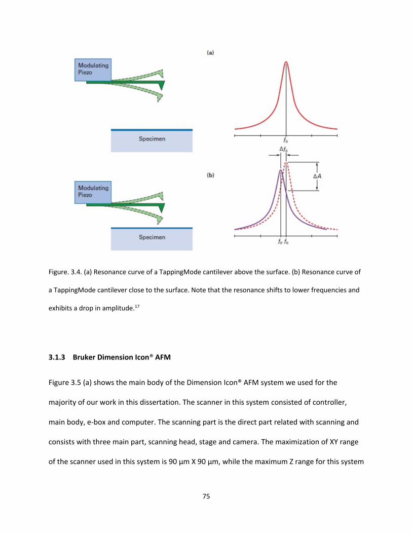
75
Figure. 3.4. (a) Resonance curve of a TappingMode cantilever above the surface. (b) Resonance curve of
a TappingMode cantilever close to the surface. Note that the resonance shifts to lower frequencies and
exhibits a drop in amplitude.17
3.1.3 Bruker Dimension Icon® AFM
Figure 3.5 (a) shows the main body of the Dimension Icon® AFM system we used for the
majority of our work in this dissertation. The scanner in this system consisted of controller,
main body, e-box and computer. The scanning part is the direct part related with scanning and
consists with three main part, scanning head, stage and camera. The maximization of XY range
of the scanner used in this system is 90 μm X 90 μm, while the maximum Z range for this system
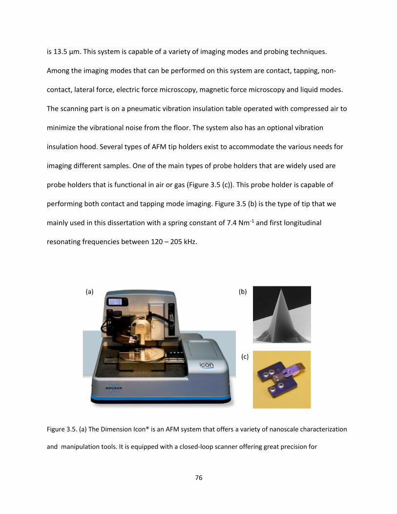
76
is 13.5 μm. This system is capable of a variety of imaging modes and probing techniques.
Among the imaging modes that can be performed on this system are contact, tapping, non-
contact, lateral force, electric force microscopy, magnetic force microscopy and liquid modes.
The scanning part is on a pneumatic vibration insulation table operated with compressed air to
minimize the vibrational noise from the floor. The system also has an optional vibration
insulation hood. Several types of AFM tip holders exist to accommodate the various needs for
imaging different samples. One of the main types of probe holders that are widely used are
probe holders that is functional in air or gas (Figure 3.5 (c)). This probe holder is capable of
performing both contact and tapping mode imaging. Figure 3.5 (b) is the type of tip that we
mainly used in this dissertation with a spring constant of 7.4 Nm-1 and first longitudinal
resonating frequencies between 120 – 205 kHz.
Figure 3.5. (a) The Dimension Icon® is an AFM system that offers a variety of nanoscale characterization
and manipulation tools. It is equipped with a closed-loop scanner offering great precision for
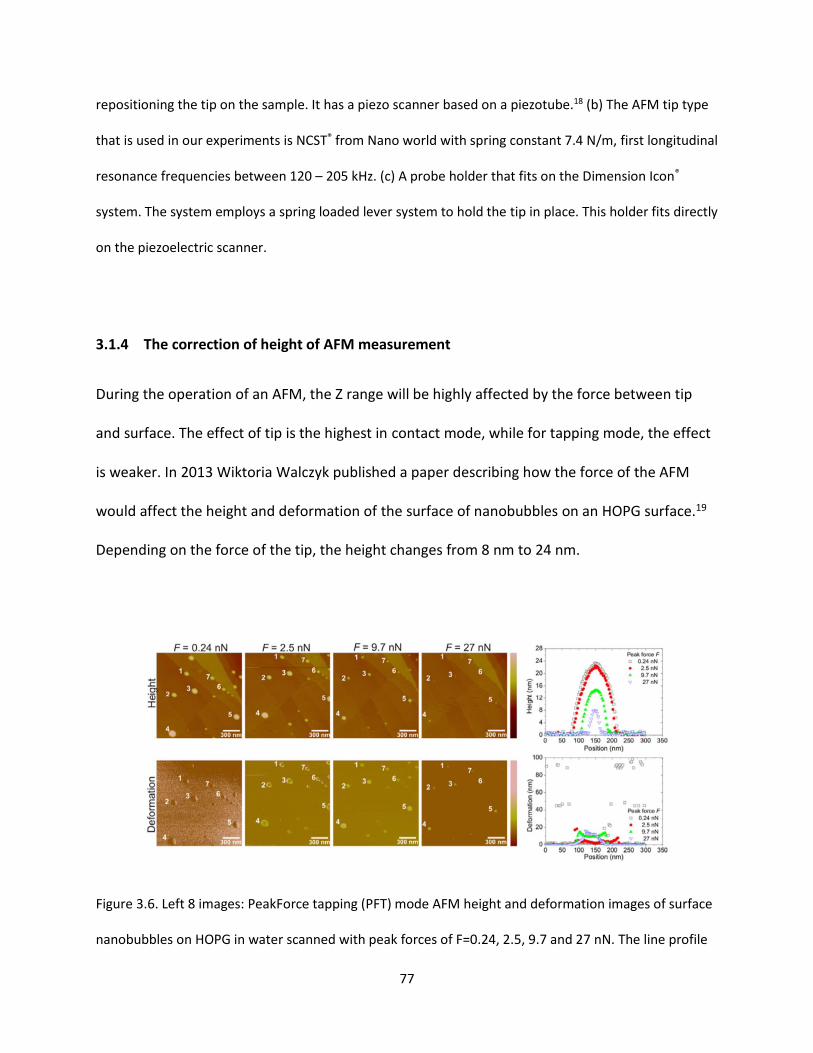
77
repositioning the tip on the sample. It has a piezo scanner based on a piezotube.18 (b) The AFM tip type
that is used in our experiments is NCST® from Nano world with spring constant 7.4 N/m, first longitudinal
resonance frequencies between 120 – 205 kHz. (c) A probe holder that fits on the Dimension Icon®
system. The system employs a spring loaded lever system to hold the tip in place. This holder fits directly
on the piezoelectric scanner.
3.1.4 The correction of height of AFM measurement
During the operation of an AFM, the Z range will be highly affected by the force between tip
and surface. The effect of tip is the highest in contact mode, while for tapping mode, the effect
is weaker. In 2013 Wiktoria Walczyk published a paper describing how the force of the AFM
would affect the height and deformation of the surface of nanobubbles on an HOPG surface.19
Depending on the force of the tip, the height changes from 8 nm to 24 nm.
Figure 3.6. Left 8 images: PeakForce tapping (PFT) mode AFM height and deformation images of surface
nanobubbles on HOPG in water scanned with peak forces of F=0.24, 2.5, 9.7 and 27 nN. The line profile
78
(cross section) of height and deformation of surface nanobubbles with peak forces F=0.24, 2.5, 9.7 and
27 nN.19
3.2 Introduction to Scanning Tunneling Microscope (STM)
Scanning Tunneling Microscope (STM) was invented by G. Binnig, H. Rohrer at the IBM Zurich
Research Lab in 1981 by observing vacuum electron tunneling between a sharp tungsten tip
and a platinum sample.20-21 They won the Nobel Prize of 1986 in Physics for their invention of
STM. Since then, STM experienced revolutionary development broadening our perception
about atomic scale processes and structure and become one of the most advanced atomic
structure probing instruments in the world. With increasing availability of low-temperature
STM, local electronic properties can be investigated with unprecedented space and energy
resolution which opens the vista to completely new applications. The sharp tip can be
considered to be a powerful local probe, allowing one to measure physical properties of
materials on a small scale by using a variety of different spectroscopic methods. A variety of
STMs with different sizes in different environments have been designed over a wide range of
pressures and temperatures.22-27
The general principle of operation of a STM is surprising simple. Figure 3.7 shows the
fundamental schematic diagram of STM. From the figure 3.7, we can see separation of the scale
of a few Angstrom unit between end of the sharp conducting tip and the scanned sample. A
tunneling current will form in this gap as the quantum tunneling effect, after a bias voltage
applied between the sharp metal tip and a conductive sample (metal or semiconductor). The
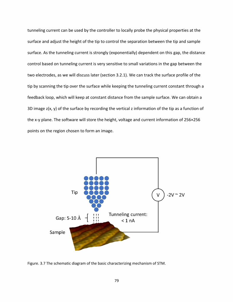
79
tunneling current can be used by the controller to locally probe the physical properties at the
surface and adjust the height of the tip to control the separation between the tip and sample
surface. As the tunneling current is strongly (exponentially) dependent on this gap, the distance
control based on tunneling current is very sensitive to small variations in the gap between the
two electrodes, as we will discuss later (section 3.2.1). We can track the surface profile of the
tip by scanning the tip over the surface while keeping the tunneling current constant through a
feedback loop, which will keep at constant distance from the sample surface. We can obtain a
3D image z(x, y) of the surface by recording the vertical z information of the tip as a function of
the x-y plane. The software will store the height, voltage and current information of 256×256
points on the region chosen to form an image.
Figure. 3.7 The schematic diagram of the basic characterizing mechanism of STM.
80
3.2.1 Working Principle: Tunneling Effect
The phenomenon that enables STM is the tunneling effect. The tunneling effect is a quantum
mechanical phenomenon in which subatomic particles pass through a classically forbidden
potential barrier. The laws of classical mechanics cannot explain quantum tunneling because
the energy required to pass the barrier is greater than the barrier.
The most important part for theoretical description of STM is how to calculate the tunneling
current. The actual tunneling current is pretty complicated due to different kinds of samples,
but we can start with the simplest model: both tip and sample are metals, separated by a tiny
vacuum gap.
According to the tunneling mechanism, the simplest equation is:
𝑑𝐼
𝑑𝑉|𝑉 ~ 𝐿𝐷𝑂𝑆𝑠𝑎𝑚𝑝𝑙𝑒(𝐸𝐹 + 𝑒𝑉) 3.1
In this equation, V is the voltage applied on the sample, I is the total tunneling current,
𝐿𝐷𝑂𝑆𝑠𝑎𝑚𝑝𝑙𝑒 are the local density of state (LDOS) for the sample and Ef is the Fermi energy.
From this equation, we see that the tunneling current conductance is in proportion to LODS of
the surface.
In 1961, Bardeen proposed the time-dependent perturbation theory that is used most widely
now.28 There are three presumptions in this theory: there is overlap in the density of state
between the tip and the sample because of the very small gap; this kind of the weak overlap
does not influence each density of states; and the wave functions exponentially drop to zero in
the gap area.
81
After using the time-dependent perturbation theory, we can get:
I𝑡→𝑠 = −2𝑒 ∙2𝜋
ℏ ∙ |𝑀𝑡𝑠|2 ∙ 𝐿𝐷𝑂𝑆𝑡𝑖𝑝(𝐸)f(E) ∙ (𝐿𝐷𝑂𝑆𝑠𝑎𝑚𝑝𝑙𝑒(𝐸 + 𝑒𝑉)[1 − 𝑓(𝐸 + 𝑒𝑉)]) 3.2
In this equation, the factor 2 is due to the spin degeneracy of the electron, -e represents the
classical negative electron charge, 2𝜋/ℏ is the factor from the time-dependent perturbation
theory, |𝑀𝑡𝑠| is the tunneling matrix influenced by the separation distance between the tip29
and the sample and f(E)=1/(1 + eE/k𝐵𝑇) is the famous Fermi Distribution.
Eq. 3.2 is the dominant tunneling current between the tip and sample, but there are also
electrons tunneling from the sample to the tip:
I𝑠→𝑡 = −2𝑒 ∙ 2𝜋
ℏ |𝑀𝑠𝑡|2 ∙ 𝐿𝐷𝑂𝑆𝑠𝑎𝑚𝑝𝑙𝑒(𝐸 + 𝑒𝑉)𝑓(E + eV) ∙ (𝐿𝐷𝑂𝑆𝑡𝑖𝑝(𝐸)[1 − 𝑓(𝐸)]) 3.3
These two tunneling currents are in opposite directions, so the total current should be the
integral over all energies E after the subtraction of Eq. 3.3 from Eq. 3.2. Then we get the total
tunneling current:
I𝑡𝑜𝑡𝑎𝑙 = −2𝑒 ∙ 2𝜋
ℏ ∙ ∫ |𝑀|2
∞
−𝐸𝐹(𝑠𝑎𝑚𝑝𝑙𝑒)∙ 𝐿𝐷𝑂𝑆𝑡𝑖𝑝(𝐸) ∙ LDOS𝑠𝑎𝑚𝑝𝑙𝑒(E + eV) ∙ {𝑓(E)[1 −
𝑓(𝐸 + 𝑒𝑉)] − [1 − 𝑓(𝐸)]𝑓(𝑒 + 𝑒𝑉) ∙ 𝑑𝐸 3.4
If we assume the temperature (T) is 0 K, then 𝑓(E ≤ E𝐹) = 1, 𝑓(E > E𝐹) = 0, so we can
simplify Eq. 3.4 to:
I𝑡𝑜𝑡𝑎𝑙 ≈ −2𝑒 ∙ 2𝜋
ℏ ∙ ∫ |𝑀|2
0
−𝐸𝐹(𝑠𝑎𝑚𝑝𝑙𝑒)∙ 𝐿𝐷𝑂𝑆𝑡𝑖𝑝(𝐸) ∙ LDOS𝑠𝑎𝑚𝑝𝑙𝑒(E + eV) ∙ 𝑑𝐸 3.5
82
For the simplest situation, the vacuum barrier is a square barrier with a smaller bias compared
to the sum of the work function of both the tip and sample, the tunneling matrix |𝑀| can
written as Eq. 3.6 under the WKB approximation:30-31
|𝑀|2 = 𝑒−2𝑠√
2𝑚
ℏ(
𝜙𝑠+𝜙𝑡2
) 3.6
where 𝜙𝑠 𝑎𝑛𝑑 𝜙𝑡 represent the work functions of the tip and sample, respectively. Finally, we
get the total tunneling current:
I𝑡𝑜𝑡𝑎𝑙 = −2𝑒 ∙ 2𝜋
ℏ ∙ 𝑒
−2𝑠√2𝑚
ℏ(
𝜙𝑠+𝜙𝑡2
)∫ 𝐿𝐷𝑂𝑆𝑡𝑖𝑝(𝐸) ∙ LDOS𝑠𝑎𝑚𝑝𝑙𝑒(E + eV) ∙ 𝑑𝐸
0
−𝐸𝐹(𝑠𝑎𝑚𝑝𝑙𝑒) 3.7
J. Tersoff, and D.R. Hamann proposed an s-wave-model to simplify the DOS of the tip to a
constant, so we can modify the tunneling current to:
I𝑡𝑜𝑡𝑎𝑙 = −2𝑒 ∙ 2𝜋
ℏ ∙ 𝑒
−2𝑠√2𝑚
ℏ(
𝜙𝑠+𝜙𝑡2
)∙ 𝐿𝐷𝑂𝑆𝑡𝑖𝑝(0) ∫ LDOS𝑠𝑎𝑚𝑝𝑙𝑒(E + eV) ∙ 𝑑𝐸
0
−𝑒𝑉 3.8
Therefore, we can differentiate Eq. 3.8 to get the Eq. 3.1:
𝑑𝐼𝑡𝑜𝑡𝑎𝑙
𝑑𝑉|𝑉 ~ 𝐿𝐷𝑂𝑆𝑠𝑎𝑚𝑝𝑙𝑒(𝐸𝐹 + 𝑒𝑉) 3.1
So, we verify that the tunneling current conductance is just in proportion to the LDOS of the
surface.
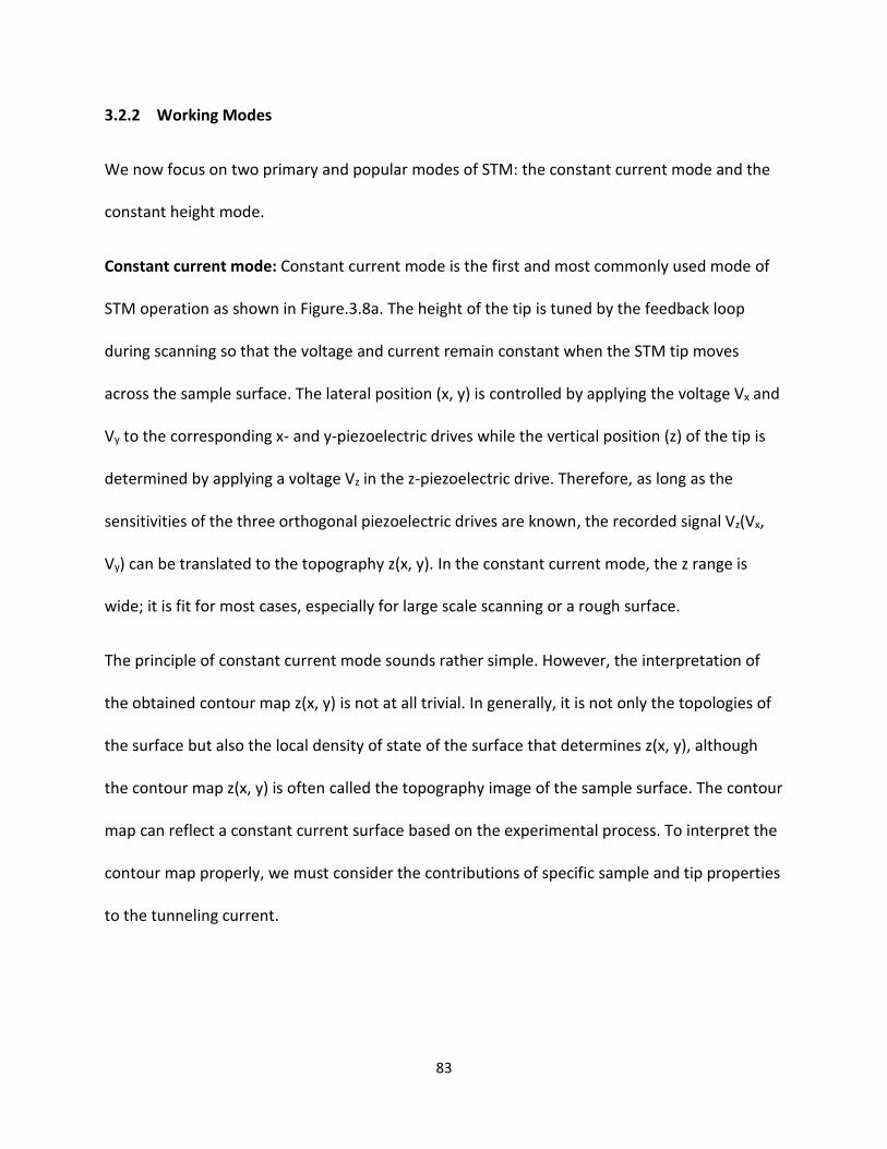
83
3.2.2 Working Modes
We now focus on two primary and popular modes of STM: the constant current mode and the
constant height mode.
Constant current mode: Constant current mode is the first and most commonly used mode of
STM operation as shown in Figure.3.8a. The height of the tip is tuned by the feedback loop
during scanning so that the voltage and current remain constant when the STM tip moves
across the sample surface. The lateral position (x, y) is controlled by applying the voltage Vx and
Vy to the corresponding x- and y-piezoelectric drives while the vertical position (z) of the tip is
determined by applying a voltage Vz in the z-piezoelectric drive. Therefore, as long as the
sensitivities of the three orthogonal piezoelectric drives are known, the recorded signal Vz(Vx,
Vy) can be translated to the topography z(x, y). In the constant current mode, the z range is
wide; it is fit for most cases, especially for large scale scanning or a rough surface.
The principle of constant current mode sounds rather simple. However, the interpretation of
the obtained contour map z(x, y) is not at all trivial. In generally, it is not only the topologies of
the surface but also the local density of state of the surface that determines z(x, y), although
the contour map z(x, y) is often called the topography image of the sample surface. The contour
map can reflect a constant current surface based on the experimental process. To interpret the
contour map properly, we must consider the contributions of specific sample and tip properties
to the tunneling current.

84
Constant height mode: A notable disadvantage of the constant current mode is the limited
response time of the feedback loop, which greatly limits data acquisition time and the scanning
speed. In principle, the scanning speed of the tip is faster than the response of the feedback.32-
33 Consequently, the feedback can not respond to the higher frequency components
modulating the tunneling current due to it has to maintain an desired tunneling current.
Alternatively, you can switch off the feedback completely. If the response to the preamplifier is
still faster than the scanning speed, the tunneling current will be exponential depend on the
spacing between the tip and surface which will reflect the morphology at the atomic scale.
The tip will be scanned at a constant z height in the constant height mode, while the tunneling
current I is measured as a function of the position. The voltage applied on the tip or sample is
constant, and the z-piezoelectric feedback system is turned off. In this case, a surface bump will
be reflected in a higher tunneling current. As the height is constant and the separation between
tip and sample is of the sub-nanometer level, the scanning area has to be very flat. The current
mainly reflects the local density of states. This mode is especially fit for small area scanning.
This constant height mode can also used to obtain STM images at video speed, which provide
the opportunity to investigate dynamic atomic level procedure at surfaces, such as surface
diffusion.
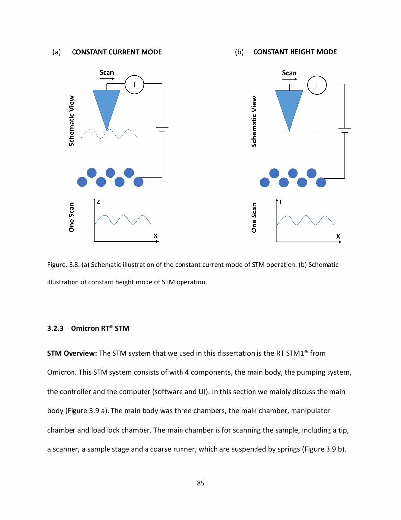
85
Figure. 3.8. (a) Schematic illustration of the constant current mode of STM operation. (b) Schematic
illustration of constant height mode of STM operation.
3.2.3 Omicron RT® STM
STM Overview: The STM system that we used in this dissertation is the RT STM1® from
Omicron. This STM system consists of with 4 components, the main body, the pumping system,
the controller and the computer (software and UI). In this section we mainly discuss the main
body (Figure 3.9 a). The main body was three chambers, the main chamber, manipulator
chamber and load lock chamber. The main chamber is for scanning the sample, including a tip,
a scanner, a sample stage and a coarse runner, which are suspended by springs (Figure 3.9 b).
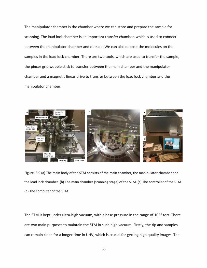
86
The manipulator chamber is the chamber where we can store and prepare the sample for
scanning. The load lock chamber is an important transfer chamber, which is used to connect
between the manipulator chamber and outside. We can also deposit the molecules on the
samples in the load lock chamber. There are two tools, which are used to transfer the sample,
the pincer grip wobble stick to transfer between the main chamber and the manipulator
chamber and a magnetic linear drive to transfer between the load lock chamber and the
manipulator chamber.
Figure. 3.9 (a) The main body of the STM consists of the main chamber, the manipulator chamber and
the load lock chamber. (b) The main chamber (scanning stage) of the STM. (c) The controller of the STM.
(d) The computer of the STM.
The STM is kept under ultra-high vacuum, with a base pressure in the range of 10-10 torr. There
are two main purposes to maintain the STM in such high vacuum. Firstly, the tip and samples
can remain clean for a longer time in UHV, which is crucial for getting high quality images. The
87
scanning gap between the tip and sample is only a few Angstroms, so a cleaner chamber has
less chance to contaminate the sample, in return. Secondly, the mechanism of the STM is that
the tunneling current go through the tip and the sample, and being in air will make the
tunneling situation more complicated, decreasing the stability of the measurement.
The STM vacuum system has four pumps, the mechanical pump, turbo pump, titanium
sublimation pump (tsp) and ion pump. The mechanical pump is a classical roughing pump or
backing pump. It is use to rough pump the system to 0.01 torr and also a backing pump to
support the turbo pump. The turbo pump is the secondary pump which provide a greater
probability of gas moving towards the outlet by transferring momentum from the rotating
blades to the molecules.34 The highest turbo vacuum system could reach as high as 10-7 torr.
After the vacuum reach as the 10-7 level, we can engage the ion pump. The ion pump is the
pump that can reach as high as 10-11 (our STM can reach 10-10 torr) by sputtering the ionized gas
to a metal gutter. After keeping the ion pump on, we can turn off the turbo pump and
mechanical pump. When the vacuum level in the main chamber is not good, we can turn on the
TSP to improve the vacuum. A high current (typically around 40 Amps, for us) is periodically
passed through TSP, which consists of a titanium filament. A thin layer of clean titanium can be
formed on the surrounding chamber walls as this current causes the filament to reach the
sublimation temperature of titanium.35 The residual gas components, colliding with the
chamber wall, tend to react and to form a solid, stable product due to the reactivity of clean
titanium in the chamber.35 Thus, the gas pressure is reduced in the chamber.
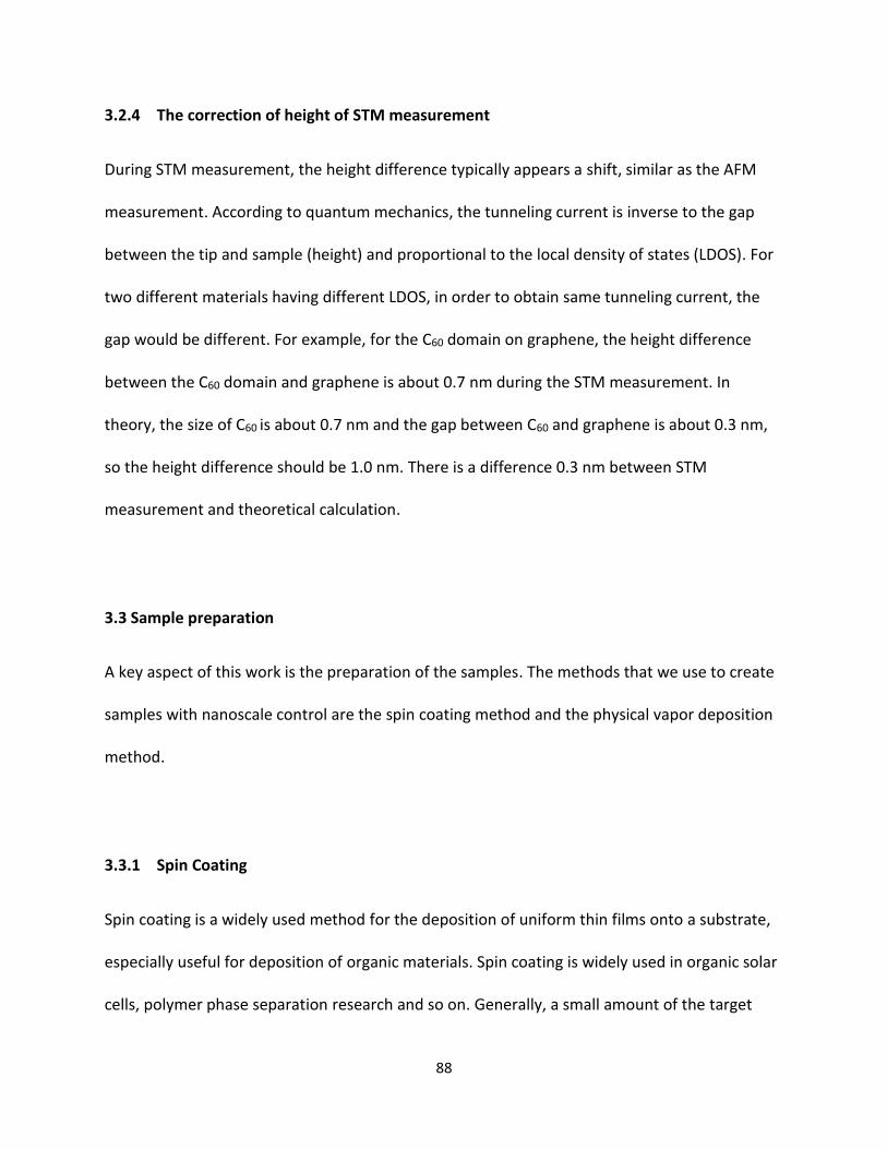
88
3.2.4 The correction of height of STM measurement
During STM measurement, the height difference typically appears a shift, similar as the AFM
measurement. According to quantum mechanics, the tunneling current is inverse to the gap
between the tip and sample (height) and proportional to the local density of states (LDOS). For
two different materials having different LDOS, in order to obtain same tunneling current, the
gap would be different. For example, for the C60 domain on graphene, the height difference
between the C60 domain and graphene is about 0.7 nm during the STM measurement. In
theory, the size of C60 is about 0.7 nm and the gap between C60 and graphene is about 0.3 nm,
so the height difference should be 1.0 nm. There is a difference 0.3 nm between STM
measurement and theoretical calculation.
3.3 Sample preparation
A key aspect of this work is the preparation of the samples. The methods that we use to create
samples with nanoscale control are the spin coating method and the physical vapor deposition
method.
3.3.1 Spin Coating
Spin coating is a widely used method for the deposition of uniform thin films onto a substrate,
especially useful for deposition of organic materials. Spin coating is widely used in organic solar
cells, polymer phase separation research and so on. Generally, a small amount of the target
89
material is dropped onto the substrate, which is either spinning at low speed or not spinning at
all, and then it is rotated at a higher speed to spread the target material by centrifugal force. In
chapter 4, we use spin coating to create monolayer or bilayer samples for AFM testing. During
the preparation, we spin coat a PCBM/Chlorobenzene solution on HOPG and graphene
substrates with a rate of 1000 rpm. The concentration of the solution that we used varied from
0.15 mg/ml to 2.0 mg/ml. Figure 3.10a is the spin coater that we used in this dissertation.
3.3.2 Physical Vapor Deposition
Physical vapor deposition (PVD) is one of the methods to create nanometer scale thin films. The
PVD method is realized by creating vapor by a physical method and then deposit the vapor on
the substrate under UHV condition. In this dissertation, the PVD method is used to create a
monolayer of C60 or PTCDA molecules in the load lock chamber. Figure 3.10 b is the home made
Knudesen cell that we used for the PVD method. The molecular powder was loaded into the
homemade Knudsen cell and mounted in the load lock of the STM system. The molecular
sources were degassed at around 20 K below the deposition temperature under a vacuum of
about 1 x 10⁻⁶ torr prior to deposition. Then molecules were deposited onto graphene at a
deposition rate around 0.5 monolayer/min with a background pressure below 1.8×10⁻⁸ torr.
Thus, we could get monolayer or sub-monolayer samples by controlling the deposition time.
90
Figure. 3.10 (a) The spin coater that we used in this dissertation. (b) The detailed structure of the
homemade Knudsen cell showing the main components inside the copper shell. 1 is CF flange, 2 is
thermocouple wire, 3 is W heating filament, 4 is glass tube, 5 is ceramic piece, 6 is hollow copper rods
(A, B, C, D), 7 is supporting rods, 8 is feedthrough.36
References:
1. Binnig, G.; Quate, C. F.; Gerber, C., Atomic Force Microscope. Phys Rev Lett 1986, 56 (9), 930-933. 2. Variola, F., Atomic force microscopy in biomaterials surface science. Phys Chem Chem Phys 2015, 17 (5), 2950-2959. 3. Horber, J. K. H.; Miles, M. J., Scanning probe evolution in biology. Science 2003, 302 (5647), 1002-1005. 4. Marshall, G. W.; Balooch, M.; Gallagher, R. R.; Gansky, S. A.; Marshall, S. J., Mechanical properties of the dentinoenamel junction: AFM studies of nanohardness, elastic modulus, and fracture. J Biomed Mater Res 2001, 54 (1), 87-95. 5. Haugstad, G., Atomic force microscopy: understanding basic modes and advanced applications. John Wiley & Sons, Inc 2012. 6. Jalili, N.; Laxminarayana, K., A review of atomic force microscopy imaging systems: application to molecular metrology and biological sciences. Mechatronics 2004, 14 (8), 907-945.
91
7. Basso, M. G., L.; Dahleh, M.; Mezic, I., Numerical analysis of complex dynamics in atomic force microscopes. Proc IEEE Conf Control Appl. Trieste, Italy 1998, 1026-1030. 8. Fung, R. F.; Huang, S. C., Dynamic modeling and vibration analysis of the atomic force microscope. J Vib Acoust 2001, 123 (4), 502-509. 9. Salapaka, M. C. D., Stability and sensitivity analysis of periodic orbits in tapping mode atomic force microscopy. Proc Conf Decision Control. Tampa FL 1998, 2047-2052. 10. Sebastian, A. S., M.; Chen, D.; Cleveland, J., Harmonic analysis based modeling of tapping-mode AFM. Proc Am Control Conf. San Diego CA 1999, 232-236. 11. http://slideplayer.com/slide/9702681/31/images/9/Modes+of+operation.+There+are+3+ modes+of+AFM+operation+Contact+mode.jpg. 12. Giessibl, F. J.; Trafas, B. M., Piezoresistive Cantilevers Utilized for Scanning Tunneling and Scanning Force Microscope in Ultrahigh-Vacuum. Rev Sci Instrum 1994, 65 (6), 1923-1929. 13. Albrecht, T. R.; Grutter, P.; Horne, D.; Rugar, D., Frequency-Modulation Detection Using High-Q Cantilevers for Enhanced Force Microscope Sensitivity. J Appl Phys 1991, 69 (2), 668-673. 14. Sugawara, Y.; Minobe, T.; Orisaka, S.; Uchihashi, T.; Tsukamoto, T.; Morita, S., Non-contact AFM images measured on Si(111)root 3 x root 3-Ag and Ag(111) surfaces. Surf Interface Anal 1999, 27 (5-6), 456-461. 15. Orisaka, S.; Minobe, T.; Uchihashi, T.; Sugawara, Y.; Morita, S., The atomic resolution imaging of metallic Ag(111) surface by noncontact atomic force microscope. Appl Surf Sci 1999, 140 (3-4), 243-246. 16. Zhong, Q.; Inniss, D.; Kjoller, K.; Elings, V. B., Fractured Polymer Silica Fiber Surface Studied by Tapping Mode Atomic-Force Microscopy. Surf Sci 1993, 290 (1-2), L688-L692. 17. https://www.azonano.com/article.aspx?ArticleID=3010. 18. https://www.bruker.com/products/surface-and-dimensional-analysis/atomic-force-microscopes/dimension-icon/overview.html. 19. Walczyk, W.; Schon, P. M.; Schonherr, H., The effect of PeakForce tapping mode AFM imaging on the apparent shape of surface nanobubbles. J Phys-Condens Mat 2013, 25 (18). 20. Binning, G.; Rohrer, H.; Gerber, C.; Weibel, E., Surface Studies by Scanning Tunneling Microscopy. Phys Rev Lett 1982, 49 (1), 57-61. 21. Binnig, G.; Rohrer, H.; Gerber, C.; Weibel, E., Tunneling through a Controllable Vacuum Gap. Appl Phys Lett 1982, 40 (2), 178-180. 22. Besenbacher, F.; Laegsgaard, E.; Mortensen, K.; Nielsen, U.; Stensgaard, I., Compact, High-Stability, Thimble-Size Scanning Tunneling Microscope. Rev Sci Instrum 1988, 59 (7), 1035-1038. 23. Mcintyre, B. J.; Salmeron, M.; Somorjai, G. A., A Variable Pressure Temperature Scanning Tunneling Microscope for Surface Science and Catalysis Studies. Rev Sci Instrum 1993, 64 (3), 687-691. 24. Besenbacher, F., Scanning tunnelling microscopy studies of metal surfaces. Rep Prog Phys 1996, 59 (12), 1737-1802. 25. Ferris, J. H.; Kushmerick, J. G.; Johnson, J. A.; Youngquist, M. G. Y.; Kessinger, R. B.; Kingsbury, H. F.; Weiss, P. S., Design, operation, and housing of an ultrastable, low temperature, ultrahigh vacuum scanning tunneling microscope. Rev Sci Instrum 1998, 69 (7), 2691-2695. 26. Jensen, J. A.; Rider, K. B.; Chen, Y.; Salmeron, M.; Somorjai, G. A., High pressure, high temperature scanning tunneling microscopy. J Vac Sci Technol B 1999, 17 (3), 1080-1084. 27. Kugler, M.; Renner, C.; Fischer, O.; Mikheev, V.; Batey, G., A He-3 refrigerated scanning tunneling microscope in high magnetic fields and ultrahigh vacuum. Rev Sci Instrum 2000, 71 (3), 1475-1478. 28. Bardeen, J., Tunnelling from a Many-Particle Point of View. Phys Rev Lett 1961, 6 (2), 57-&. 29. Chenggang, T., LUCTUATIONS ON METAL SURFACES AND MOLECULE/METAL INTERFACES PhD thesis. University of Maryland 2007. 30. Chen, C. J., Introduction to scanning tunneling microscopy. Oxford University Press 1993.
92
31. Wiesendanger, R., Contributions of Scanning Probe Microscopy and Spectroscopy to the Investigation and Fabrication of Nanometer-Scale Structures. J Vac Sci Technol B 1994, 12 (2), 515-529. 32. Bryant, A.; Smith, D. P. E.; Quate, C. F., Imaging in Real-Time with the Tunneling Microscope. Appl Phys Lett 1986, 48 (13), 832-834. 33. Bryant, A.; Smith, D. P. E.; Binnig, G.; Harrison, W. A.; Quate, C. F., Anomalous Distance Dependence in Scanning Tunneling Microscopy. Appl Phys Lett 1986, 49 (15), 936-938. 1. Binnig, G.; Quate, C. F.; Gerber, C., Atomic Force Microscope. Phys Rev Lett 1986, 56 (9), 930-933. 2. Variola, F., Atomic force microscopy in biomaterials surface science. Phys Chem Chem Phys 2015, 17 (5), 2950-2959. 3. Horber, J. K. H.; Miles, M. J., Scanning probe evolution in biology. Science 2003, 302 (5647), 1002-1005. 4. Marshall, G. W.; Balooch, M.; Gallagher, R. R.; Gansky, S. A.; Marshall, S. J., Mechanical properties of the dentinoenamel junction: AFM studies of nanohardness, elastic modulus, and fracture. J Biomed Mater Res 2001, 54 (1), 87-95. 5. Haugstad, G., Atomic force microscopy: understanding basic modes and advanced applications. John Wiley & Sons, Inc 2012. 6. Jalili, N.; Laxminarayana, K., A review of atomic force microscopy imaging systems: application to molecular metrology and biological sciences. Mechatronics 2004, 14 (8), 907-945. 7. Basso, M. G., L.; Dahleh, M.; Mezic, I., Numerical analysis of complex dynamics in atomic force microscopes. Proc IEEE Conf Control Appl. Trieste, Italy 1998, 1026-1030. 8. Fung, R. F.; Huang, S. C., Dynamic modeling and vibration analysis of the atomic force microscope. J Vib Acoust 2001, 123 (4), 502-509. 9. Salapaka, M. C. D., Stability and sensitivity analysis of periodic orbits in tapping mode atomic force microscopy. Proc Conf Decision Control. Tampa FL 1998, 2047-2052. 10. Sebastian, A. S., M.; Chen, D.; Cleveland, J., Harmonic analysis based modeling of tapping-mode AFM. Proc Am Control Conf. San Diego CA 1999, 232-236. 11. http://slideplayer.com/slide/9702681/31/images/9/Modes+of+operation.+There+are+3+ modes+of+AFM+operation+Contact+mode.jpg 12. Giessibl, F. J.; Trafas, B. M., Piezoresistive Cantilevers Utilized for Scanning Tunneling and Scanning Force Microscope in Ultrahigh-Vacuum. Rev Sci Instrum 1994, 65 (6), 1923-1929. 13. Albrecht, T. R.; Grutter, P.; Horne, D.; Rugar, D., Frequency-Modulation Detection Using High-Q Cantilevers for Enhanced Force Microscope Sensitivity. J Appl Phys 1991, 69 (2), 668-673. 14. Sugawara, Y.; Minobe, T.; Orisaka, S.; Uchihashi, T.; Tsukamoto, T.; Morita, S., Non-contact AFM images measured on Si(111)root 3 x root 3-Ag and Ag(111) surfaces. Surf Interface Anal 1999, 27 (5-6), 456-461. 15. Orisaka, S.; Minobe, T.; Uchihashi, T.; Sugawara, Y.; Morita, S., The atomic resolution imaging of metallic Ag(111) surface by noncontact atomic force microscope. Appl Surf Sci 1999, 140 (3-4), 243-246. 16. Zhong, Q.; Inniss, D.; Kjoller, K.; Elings, V. B., Fractured Polymer Silica Fiber Surface Studied by Tapping Mode Atomic-Force Microscopy. Surf Sci 1993, 290 (1-2), L688-L692. 17. https://www.azonano.com/article.aspx?ArticleID=3010. 18. https://www.bruker.com/products/surface-and-dimensional-analysis/atomic-force-microscopes/dimension-icon/overview.html. 19. Walczyk, W.; Schon, P. M.; Schonherr, H., The effect of PeakForce tapping mode AFM imaging on the apparent shape of surface nanobubbles. J Phys-Condens Mat 2013, 25 (18). 20. Binning, G.; Rohrer, H.; Gerber, C.; Weibel, E., Surface Studies by Scanning Tunneling Microscopy. Phys Rev Lett 1982, 49 (1), 57-61.
93
21. Binnig, G.; Rohrer, H.; Gerber, C.; Weibel, E., Tunneling through a Controllable Vacuum Gap. Appl Phys Lett 1982, 40 (2), 178-180. 22. Besenbacher, F.; Laegsgaard, E.; Mortensen, K.; Nielsen, U.; Stensgaard, I., Compact, High-Stability, Thimble-Size Scanning Tunneling Microscope. Rev Sci Instrum 1988, 59 (7), 1035-1038. 23. Mcintyre, B. J.; Salmeron, M.; Somorjai, G. A., A Variable Pressure Temperature Scanning Tunneling Microscope for Surface Science and Catalysis Studies. Rev Sci Instrum 1993, 64 (3), 687-691. 24. Besenbacher, F., Scanning tunnelling microscopy studies of metal surfaces. Rep Prog Phys 1996, 59 (12), 1737-1802. 25. Ferris, J. H.; Kushmerick, J. G.; Johnson, J. A.; Youngquist, M. G. Y.; Kessinger, R. B.; Kingsbury, H. F.; Weiss, P. S., Design, operation, and housing of an ultrastable, low temperature, ultrahigh vacuum scanning tunneling microscope. Rev Sci Instrum 1998, 69 (7), 2691-2695. 26. Jensen, J. A.; Rider, K. B.; Chen, Y.; Salmeron, M.; Somorjai, G. A., High pressure, high temperature scanning tunneling microscopy. J Vac Sci Technol B 1999, 17 (3), 1080-1084. 27. Kugler, M.; Renner, C.; Fischer, O.; Mikheev, V.; Batey, G., A He-3 refrigerated scanning tunneling microscope in high magnetic fields and ultrahigh vacuum. Rev Sci Instrum 2000, 71 (3), 1475-1478. 28. Bardeen, J., Tunnelling from a Many-Particle Point of View. Phys Rev Lett 1961, 6 (2), 57-&. 29. Chenggang, T., LUCTUATIONS ON METAL SURFACES AND MOLECULE/METAL INTERFACES PhD thesis. University of Maryland 2007. 30. Chen, C. J., Introduction to scanning tunneling microscopy. Oxford University Press 1993. 31. Wiesendanger, R., Contributions of Scanning Probe Microscopy and Spectroscopy to the Investigation and Fabrication of Nanometer-Scale Structures. J Vac Sci Technol B 1994, 12 (2), 515-529. 32. Bryant, A.; Smith, D. P. E.; Quate, C. F., Imaging in Real-Time with the Tunneling Microscope. Appl Phys Lett 1986, 48 (13), 832-834. 33. Bryant, A.; Smith, D. P. E.; Binnig, G.; Harrison, W. A.; Quate, C. F., Anomalous Distance Dependence in Scanning Tunneling Microscopy. Appl Phys Lett 1986, 49 (15), 936-938. 34. https://vacaero.com/information-resources/vacuum-pump-technology-education-and-training/1039-an-introduction-to-vacuum-pumps.html. 35. https://en.wikipedia.org/wiki/Titanium_sublimation_pump#cite_note-vacgen-1. 36. Chuanhui Y. , A. M., Husong Z. , Yanlong L. , Chenggang T., Preparation and Characterization of C60/Graphene Hybrid Nanostructures. Journal of Visualized Experiments 2018, 135 (e57257).
94 This chapter closely follows the publication: Li, Y.; Chen, C.; Burton, J.; Park, K.; Heflin, J.; Tao, C., Self-Assembled PCBM Bilayers on Graphene and HOPG Examined by AFM and STM, Nanotechnology 29, 185703 (2018)
Chapter 4
Self-Assembled PCBM Bilayers on Graphene and HOPG
Examined by AFM and STM
The majority of this chapter is from a manuscript published in Institute of Physics (IOP)
nanotechnology, with slight modifications.1 The experimental part of this chapter is done by
Yanlong Li with the help of Chuanhui Chen. The discussion part is due to the effort of Yanlong Li,
Chuanhui Chen and John Burton.
4.1 Introduction
In the past several decades, organic solar cells have attracted tremendous scientific and
industrial interest because their power conversion efficiency has dramatically increased and
reached 17 % to date. 2-5 In addition, organic solar cells have potential advantages compared to
traditional solar cells in flexibility of chemical modification as well as low-cost mass production.6
Typically, an organic solar cell generates electric current through photon-induced electron
transfer that separates electrons from holes.7 the behavior of a solar cell depends on the
materials serving as electron donor and electron acceptor, respectively. As light enters a solar
cell, the photons induce electrons to transfer from the excited state of the donor to the lowest
unoccupied molecular orbital (LUMO) of the acceptor. Subsequently, the separated electrons
and holes reach the cathode and anode, respectively, delivering a direct current to an outer
95
circuit.8 The power conversion efficiency of a solar cell depends on various properties including
electron affinity of electron acceptor.
The overall performance of organic solar cells hinges on material properties of an active layer,
which is composed of a variety of donors (e.g., poly[2-methoxy-5-(3′,7′-dimethyloctyloxy)-1,4-
phenylenevinylene] (MDMO-PPV), poly(3-hexylthiophene-2,5-diyl) (P3HT)5, 9-12 ) and acceptors
(e.g., phenyl-C61-butyric acid methyl ester (PCBM)13-14). There have been intensive previous
investigations on the various factors that impact the efficiency of organic solar cell devices, such
as solvent/thermal annealing, weight ratio of donor and acceptor, thickness of the active layer,
etc.15-18 In the past several years, utilization of emerging two-dimensional (2D) materials such as
graphene for energy-related applications has attracted major research efforts.19-21 Notably,
graphene is a promising candidate for a transparent electrode material in solar cells.22-25 To
design efficient organic/2D material hybrid solar cells, it is crucial to understand the
morphology of the donor/acceptor nanostructures on 2D materials. Although morphology of
donor/acceptor nanostructures has been well characterized on bulk substrates, such as metals
or ITO,16, 26-38 similar studies on 2D materials are still lacking.
In this work, we present the self-assembled structure of PCBM, a promising acceptor material
for organic solar cells, deposited on graphene and HOPG. We discover novel bilayer
nanostructures of PCBM on graphene and HOPG, and investigate how thermal annealing tunes
the morphology of the PCBM bilayer, by using AFM and STM. Interestingly, PCBM bilayers are
formed with two typical heights on HOPG, but only one on graphene. At different annealing
temperatures, edge diffusion causes neighboring vacancies to emerge into a more ordered
structure. This first experimental realization of PCBM bilayer structures on graphene may pave
96
a way to fabricate hybrid structures of organic donor/acceptor molecules and graphene for
applications in organic solar cells.
4.2 Experimental Methods
PCBM was purchased from NanoC Inc. (Purity: 99.5%). A solution of PCBM was prepared by
stirring PCBM powder in chlorobenzene and then the solution was set on a hot plate at about
70 °C for 24 hours. The film samples were prepared by spin-coating the solution onto freshly
cleaved HOPG substrates (SPI-1 grade, purchased from SPI supplies) or graphene on Cu foils
synthesized by CVD. AFM measurements were carried out on a Dimension Icon (Bruker
Corporation) instrument in a dark environment. Monolithic silicon cantilevers (NCST, NANO
WORLD) with a spring constant of 7.4 N/m, first longitudinal resonance frequencies between
120 – 205 kHz, and nominal tip radius of 8 nm were employed in soft tapping mode.
Simultaneous height and phase images were acquired and reproduced across multiple samples.
STM characterizations were carried out in an ultra-high vacuum (UHV) scanning tunneling
microscope system (Omicron STM) with a base pressure of low 10-9 Torr. The STM tip was a
chemically etched tungsten tip.
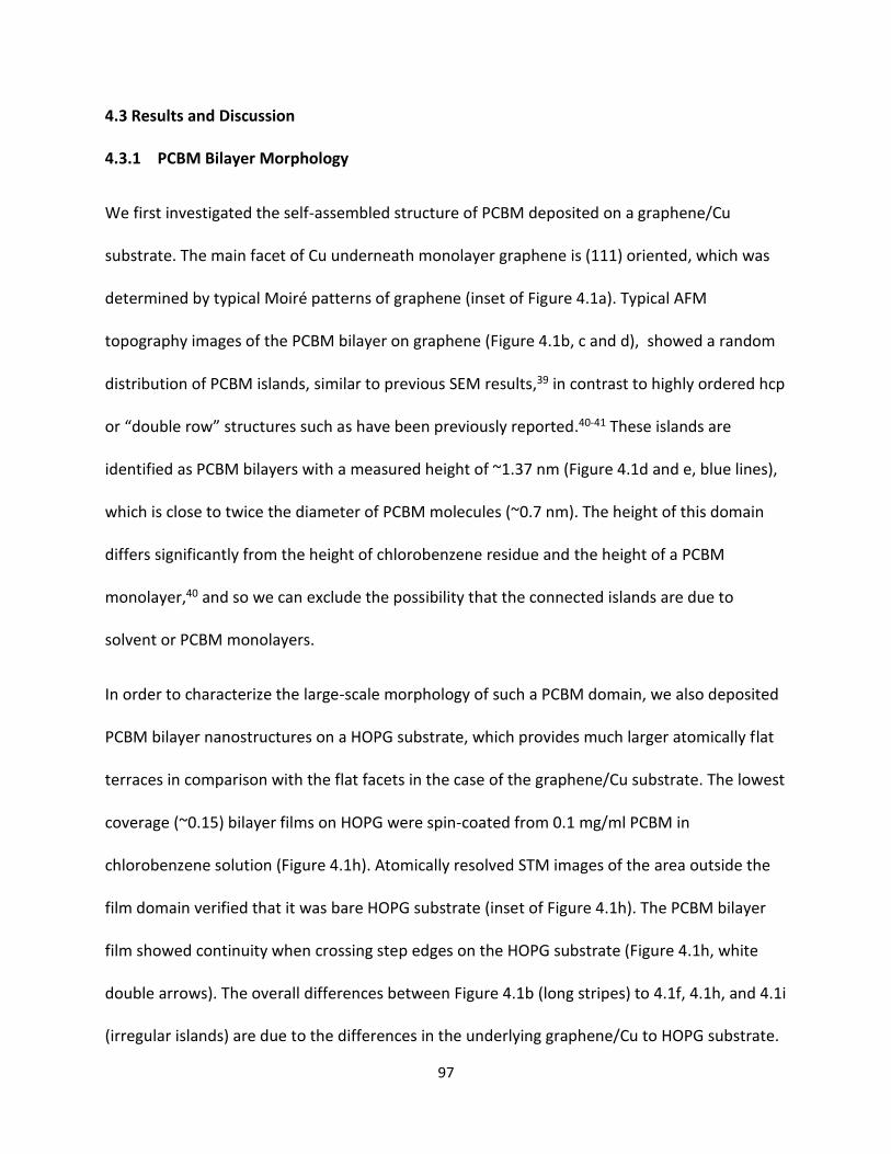
97
4.3 Results and Discussion
4.3.1 PCBM Bilayer Morphology
We first investigated the self-assembled structure of PCBM deposited on a graphene/Cu
substrate. The main facet of Cu underneath monolayer graphene is (111) oriented, which was
determined by typical Moiré patterns of graphene (inset of Figure 4.1a). Typical AFM
topography images of the PCBM bilayer on graphene (Figure 4.1b, c and d), showed a random
distribution of PCBM islands, similar to previous SEM results,39 in contrast to highly ordered hcp
or “double row” structures such as have been previously reported.40-41 These islands are
identified as PCBM bilayers with a measured height of ~1.37 nm (Figure 4.1d and e, blue lines),
which is close to twice the diameter of PCBM molecules (~0.7 nm). The height of this domain
differs significantly from the height of chlorobenzene residue and the height of a PCBM
monolayer,40 and so we can exclude the possibility that the connected islands are due to
solvent or PCBM monolayers.
In order to characterize the large-scale morphology of such a PCBM domain, we also deposited
PCBM bilayer nanostructures on a HOPG substrate, which provides much larger atomically flat
terraces in comparison with the flat facets in the case of the graphene/Cu substrate. The lowest
coverage (~0.15) bilayer films on HOPG were spin-coated from 0.1 mg/ml PCBM in
chlorobenzene solution (Figure 4.1h). Atomically resolved STM images of the area outside the
film domain verified that it was bare HOPG substrate (inset of Figure 4.1h). The PCBM bilayer
film showed continuity when crossing step edges on the HOPG substrate (Figure 4.1h, white
double arrows). The overall differences between Figure 4.1b (long stripes) to 4.1f, 4.1h, and 4.1i
(irregular islands) are due to the differences in the underlying graphene/Cu to HOPG substrate.
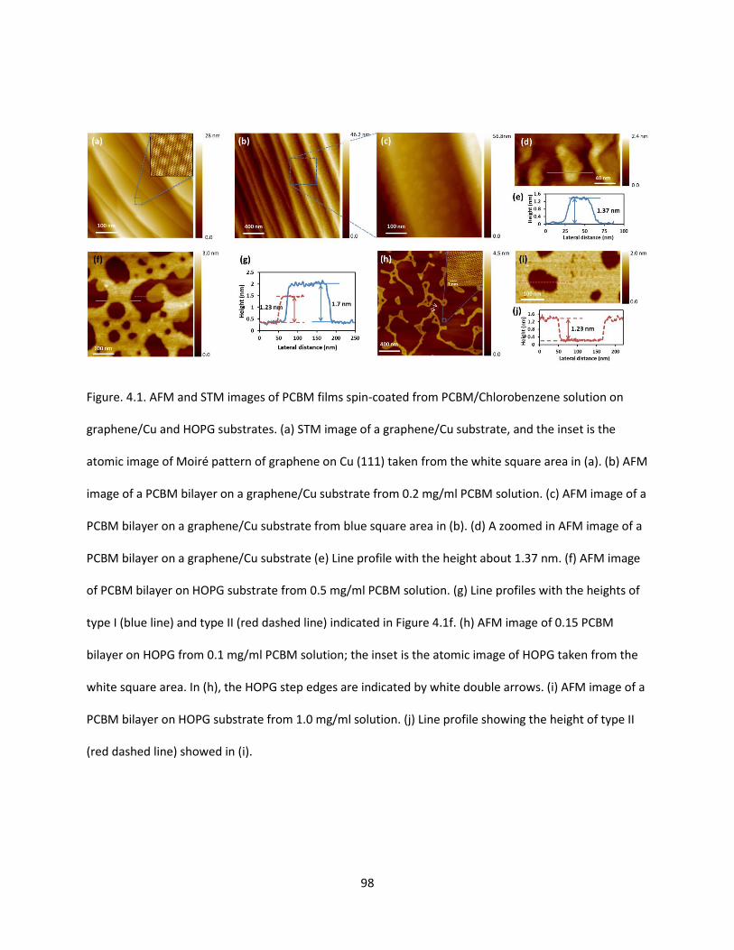
98
Figure. 4.1. AFM and STM images of PCBM films spin-coated from PCBM/Chlorobenzene solution on
graphene/Cu and HOPG substrates. (a) STM image of a graphene/Cu substrate, and the inset is the
atomic image of Moiré pattern of graphene on Cu (111) taken from the white square area in (a). (b) AFM
image of a PCBM bilayer on a graphene/Cu substrate from 0.2 mg/ml PCBM solution. (c) AFM image of a
PCBM bilayer on a graphene/Cu substrate from blue square area in (b). (d) A zoomed in AFM image of a
PCBM bilayer on a graphene/Cu substrate (e) Line profile with the height about 1.37 nm. (f) AFM image
of PCBM bilayer on HOPG substrate from 0.5 mg/ml PCBM solution. (g) Line profiles with the heights of
type I (blue line) and type II (red dashed line) indicated in Figure 4.1f. (h) AFM image of 0.15 PCBM
bilayer on HOPG from 0.1 mg/ml PCBM solution; the inset is the atomic image of HOPG taken from the
white square area. In (h), the HOPG step edges are indicated by white double arrows. (i) AFM image of a
PCBM bilayer on HOPG substrate from 1.0 mg/ml solution. (j) Line profile showing the height of type II
(red dashed line) showed in (i).
99
Strikingly, we found two typical heights in the PCBM bilayer deposited on the HOPG substrate:
1.64 ± 0.09 nm (Type I, blue line in Figure 4.1f), and 1.23 ± 0.03 nm (Type II, red lines in Figure
4.1f, i). In some films, one type of PCBM bilayer dominated the sample (Figure 4.1i), while in
others the two types coexisted in a sample (Figure 4.1f). Our observations of PCBM
monolayers, which will be discussed in the following section, showed a very different height,
and hence we exclude the possibility that the Type II structure originates from a monolayer.
Combining the above observations together, we conjecture that the height difference reflects
two distinct types of the PCBM dimer-HOPG substrate interaction with different arrangement
angles leading to different heights.
Note that these novel PCBM bilayers were observed on graphene and HOPG surfaces rather
than monolayers with hexagonal close-packed structures30, 40 or double row structures on Au
surfaces.40-41 The typical height of a PCBM monolayer is about 0.7 nm, and the height of a
PCBM bilayer is 1.64 nm. It is most likely that the observed PCBM bilayer structure consists of
PCBM dimers standing up on the graphene surface with some tilt angle due to the weak
interaction between PCBM dimers and the graphene surface. The tilt angle between PCBM
dimers and the graphene surface is about 40.6o. In a previous theoretical study, Bredas’ group
found a similar structure where pentacene molecules on a gold surface are tilted with an angle
of about 37.7°.42
Spin-coating from higher concentrations of PCBM resulted in higher coverage of the substrate
by PCBM bilayers (Figure 4.2.a-e), but the morphology of the bilayer remained as irregular
networks with randomly distributed holes. Obvious, with the increasing the concentrations of
PCBM, the coverage almost increases linearly until to a fully coverage (Figure 4.2.f).
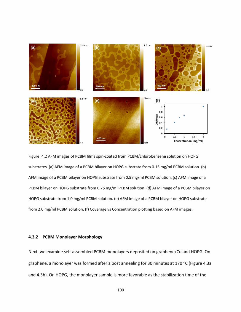
100
Figure. 4.2 AFM images of PCBM films spin-coated from PCBM/chlorobenzene solution on HOPG
substrates. (a) AFM image of a PCBM bilayer on HOPG substrate from 0.15 mg/ml PCBM solution. (b)
AFM image of a PCBM bilayer on HOPG substrate from 0.5 mg/ml PCBM solution. (c) AFM image of a
PCBM bilayer on HOPG substrate from 0.75 mg/ml PCBM solution. (d) AFM image of a PCBM bilayer on
HOPG substrate from 1.0 mg/ml PCBM solution. (e) AFM image of a PCBM bilayer on HOPG substrate
from 2.0 mg/ml PCBM solution. (f) Coverage vs Concentration plotting based on AFM images.
4.3.2 PCBM Monolayer Morphology
Next, we examine self-assembled PCBM monolayers deposited on graphene/Cu and HOPG. On
graphene, a monolayer was formed after a post annealing for 30 minutes at 170 oC (Figure 4.3a
and 4.3b). On HOPG, the monolayer sample is more favorable as the stabilization time of the
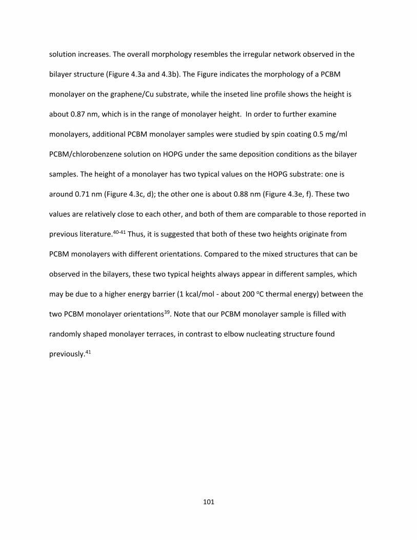
101
solution increases. The overall morphology resembles the irregular network observed in the
bilayer structure (Figure 4.3a and 4.3b). The Figure indicates the morphology of a PCBM
monolayer on the graphene/Cu substrate, while the inseted line profile shows the height is
about 0.87 nm, which is in the range of monolayer height. In order to further examine
monolayers, additional PCBM monolayer samples were studied by spin coating 0.5 mg/ml
PCBM/chlorobenzene solution on HOPG under the same deposition conditions as the bilayer
samples. The height of a monolayer has two typical values on the HOPG substrate: one is
around 0.71 nm (Figure 4.3c, d); the other one is about 0.88 nm (Figure 4.3e, f). These two
values are relatively close to each other, and both of them are comparable to those reported in
previous literature.40-41 Thus, it is suggested that both of these two heights originate from
PCBM monolayers with different orientations. Compared to the mixed structures that can be
observed in the bilayers, these two typical heights always appear in different samples, which
may be due to a higher energy barrier (1 kcal/mol - about 200 oC thermal energy) between the
two PCBM monolayer orientations39. Note that our PCBM monolayer sample is filled with
randomly shaped monolayer terraces, in contrast to elbow nucleating structure found
previously.41
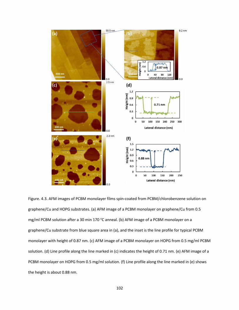
102
Figure. 4.3. AFM images of PCBM monolayer films spin-coated from PCBM/chlorobenzene solution on
graphene/Cu and HOPG substrates. (a) AFM image of a PCBM monolayer on graphene/Cu from 0.5
mg/ml PCBM solution after a 30 min 170 oC anneal. (b) AFM image of a PCBM monolayer on a
graphene/Cu substrate from blue square area in (a), and the inset is the line profile for typical PCBM
monolayer with height of 0.87 nm. (c) AFM image of a PCBM monolayer on HOPG from 0.5 mg/ml PCBM
solution. (d) Line profile along the line marked in (c) indicates the height of 0.71 nm. (e) AFM image of a
PCBM monolayer on HOPG from 0.5 mg/ml solution. (f) Line profile along the line marked in (e) shows
the height is about 0.88 nm.
103
4.3.3 Discussion
To understand the observed bilayer and monolayer structures, we constract molecular models
based on van der Waals interactions between neighboring fullerene moieties, hydrogen-
bonding between tail functional groups, and the interactions between molecules and
substrates. We first discuss the model for the monolayer structure. We propose that the two
typical monolayer heights of ~0.9 nm and ~0.7 nm observed in the PCBM monolayers reflect
different orientations of the PCBM relative to the substrate. The thicker monolayer (~0.9 nm)
corresponds to a vertical configuration of PCBM, with its tail perpendicular to the HOPG surface
(Figure 4.4a), whereas the thinner monolayer (~0.7 nm) corresponds to a horizontal
configuration, with PCBM tails parallel to the HOPG surface and interacting in pairs (Figure
4.4b). The monolayer height of 0.7 nm is consistent with the previous measurement of the size
of C60 by Robey’s group40, while the monolayer height of 0.9 nm has never been reported.
Now we turn to the small differences between the modeled and measured heights of a PCBM
monolayer in both of the proposed configurations. These differences arise from the fact that
the tapping mode AFM tends to underestimate the height of sample surface features, and that
the underestimate amount depends on the stiffness of the measured areas.43-44 For the
horizontal configuration, the actual monolayer height should be ~1 nm, because the
equilibrium van der Waals gap between C60 and the HOPG substrate is calculated to be 0.25~0.3
nm wide (Figure 4.4).40 But due to pressure exerted by the AFM tip, the monolayer height was
measured at ~0.7 nm. In fact, this measured value is comparable to a previous AFM tapping
mode image of a C60 shuttlecocks monolayer on HOPG.43 For the vertical configuration, the
monolayer height that the model suggests is 1.45 nm, marking an even larger difference from
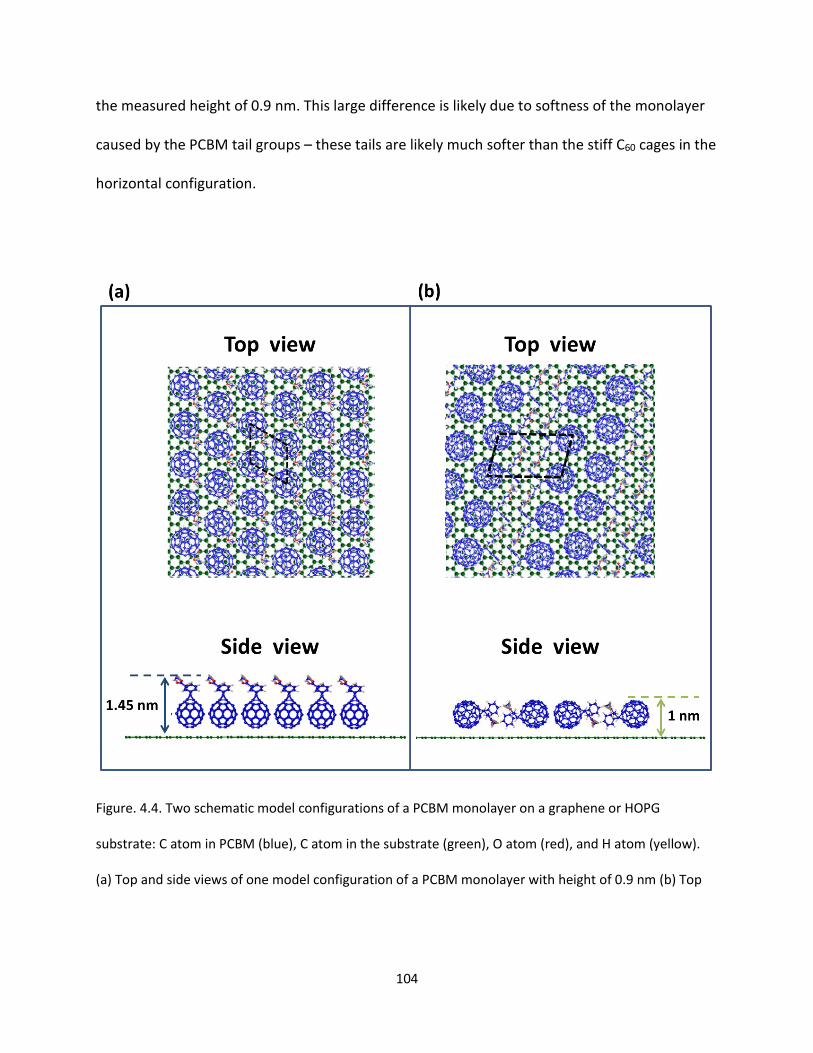
104
the measured height of 0.9 nm. This large difference is likely due to softness of the monolayer
caused by the PCBM tail groups – these tails are likely much softer than the stiff C60 cages in the
horizontal configuration.
Figure. 4.4. Two schematic model configurations of a PCBM monolayer on a graphene or HOPG
substrate: C atom in PCBM (blue), C atom in the substrate (green), O atom (red), and H atom (yellow).
(a) Top and side views of one model configuration of a PCBM monolayer with height of 0.9 nm (b) Top
105
and side views of another model configuration of a PCBM monolayer sample of with height of 0.7 nm.
The dashed parallelograms in (a) and (b) indicate unit cells.
Our analysis also suggests that a higher coverage of the monolayer favors the vertical
configuration. This is reasonable because this configuration can accommodate a much higher
area density (1.15 molecule/nm2) of PCBM than that of the horizontal configuration (0.73
molecule/nm2). Using the energy values of neighboring fullerene moieties, the hydrogen-
bonding, and the interactions between molecules and substrates from previous experimental
and theoretical investigations,40-41, 45 we calculated the formation energy of these two
configurations and the results show an energy barrier of about 1 kcal/mol exists between the
two configurations, which inhibits a thermally-induced transition between the configurations at
room temperature.
We now discuss the model for the PCBM bilayer. In most cases, we observed PCBM bilayers
rather than monolayers on graphene and HOPG. As described before, there are two typical
heights in PCBM bilayers on graphene and HOPG: 1.64 nm (modeled in Figure 4.5a), and 1.23
nm (modeled in Figure 4.5b). It was previouly reported that on a gold substrate, PCBM dimers
are formed with a twin chain structure in low density, but with a double row structure in high
density,39-40, 45 because the affinity between C60 cages (0.28 eV)46-48 is higher than the hydrogen
bonding between the PCBM tail groups (0.114 eV).46 However, in this work, PCBM molecules
were deposited by spin coating rather than physical vapor deposition. It is known that steric
hindrance of sidechain-substituted PCBM molecules would forbid a possibility of a C60-to-C60
coordinated structure in the region defined by their first solvation shells.49 Considering
106
hydrogen bonding and dipole-dipole interactions, the energy of a side-to-side dimer (0.114 eV)
is higher than side-to-C60 dimer (0.001 eV).46 Hence, we suggest that the PCBM molecules form
side-to-side dimers in the chlorobenzene solvent before the spin coating. After the spin coating,
the side-to-side PCBM dimers are distributed on the HOPG, forming the PCBM bilayers (type I
and type II in Figure 4.5). For the thicker bilayer, we propose that the PCBM dimers form a
‘double hcp’ structure: one C60 cell of the dimer lies in the lower layer, the other in the upper
layer, such that neighboring PCBM dimers interact sideways (Type I, Figure 4.5a). For the
thinner bilayer, the PCBM monomers in each dimer are also located in the lower and upper
layers (Type II, Figure 4.5b), but without strong sideways interactions between PCBM dimers.
The two typical PCBM bilayer heights indicates the different tilt angles between a PCBM dimer
and the substrate in the two configurations. A tilt angle of 49.4o corresponds to the 1.64 nm
bilayer, while a tilt angle of 60.8o the 1.23 nm bilayer, where the tilt angle is defined to be an
angle between an axis connecting the centers of two C60 in a given dimer and the direction
normal to the substrate. Similarly to the PCBM monolayer case, the measured heights of a
PCBM bilayer are ~ 0.3 nm smaller than those predicted by the model in both configurations.
These differences can be similarly explained by the compression caused by the AFM tips.
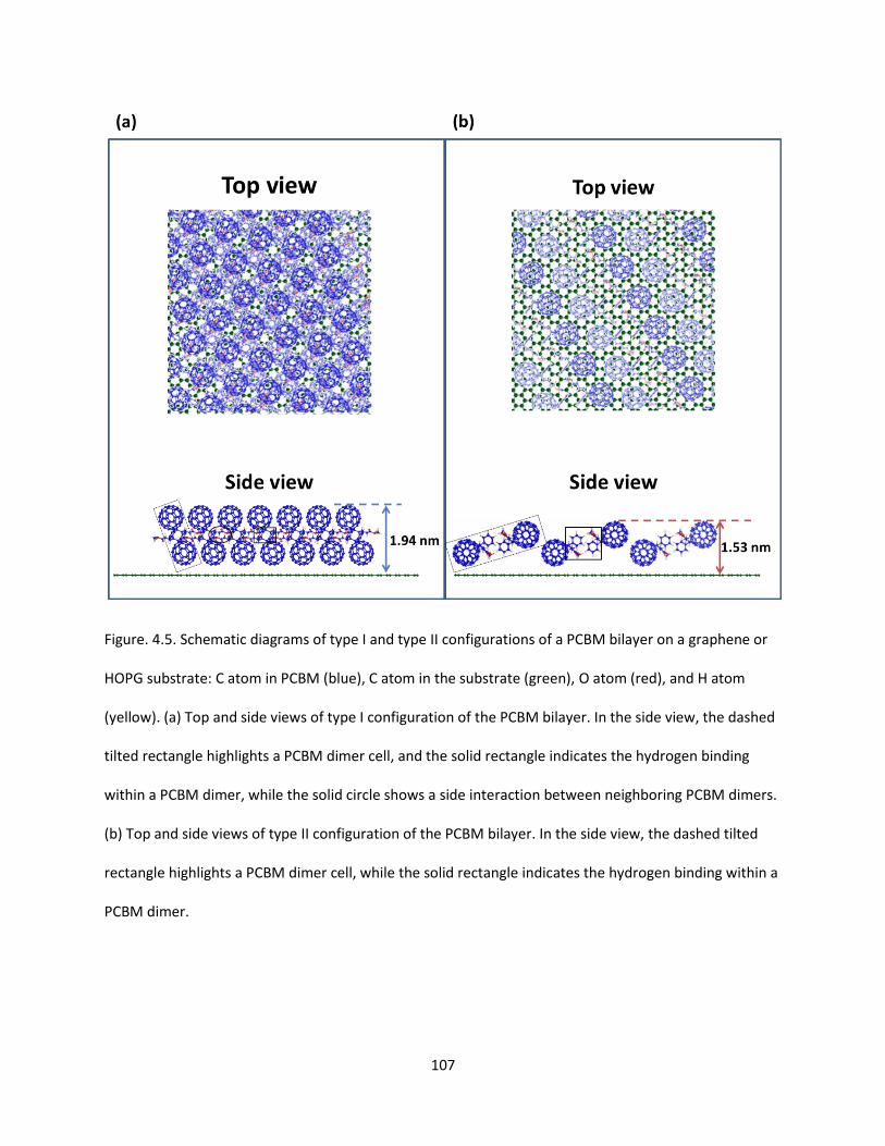
107
Figure. 4.5. Schematic diagrams of type I and type II configurations of a PCBM bilayer on a graphene or
HOPG substrate: C atom in PCBM (blue), C atom in the substrate (green), O atom (red), and H atom
(yellow). (a) Top and side views of type I configuration of the PCBM bilayer. In the side view, the dashed
tilted rectangle highlights a PCBM dimer cell, and the solid rectangle indicates the hydrogen binding
within a PCBM dimer, while the solid circle shows a side interaction between neighboring PCBM dimers.
(b) Top and side views of type II configuration of the PCBM bilayer. In the side view, the dashed tilted
rectangle highlights a PCBM dimer cell, while the solid rectangle indicates the hydrogen binding within a
PCBM dimer.
108
We further estimate the energy per unit area for the different monolayer and bilayer
configurations in order to deduce their relative stability. For Type I bilayer, the binding energy
of one upper layer cell of PCBM is 2.52 eV, which arises from the sum of the binding energy of
the 9 nearest C60 molecules with 0.28 eV each; for the lower layer PCBM cells, the binding
energies are 3.5 eV each, which arises from the sum of the binding energy of the 9 nearest C60
molecules and of the binding energy between C60 and the HOPG (0.98 eV).45, 50 Combining the
above information with hydrogen binding energies of the neighboring tail groups, we find that
the total energy for each Type I PCBM dimer is 6.13 eV. For Type II bilayer, the upper-layer
PCBM cell only has a binding energy of 1.12 eV (4 nearest C60), while the lower-layer PCBM cell
on HOPG has a binding energy of 2.1 eV, considering the binding energy of one C60 and HOPG
and the binding energy of the nearest C60 molecules. The binding energy of each PCBM dimer is
3.33 eV. Combining the above information with the hydrogen bonding of the tail groups, we
find that for the horizontal configuration the binding energy one type II PCBM dimer is 4.31 eV.
Considering the dimer concentration density of 1.15 dimer/nm2, we find that the energy
density of Type I PCBM bilayer is 7.05 eV/nm2, which is higher than that of Type II bilayer by
1.35 eV/nm2 and that of the horizontal monolayer by 1.57 eV/nm2). As concentration density
increases, the PCBM dimers are compressed to form more vertical configurations in order to
accommodate more PCBM dimers on the HOPG surface.
109
4.3.4 Thermal Effects
We now investigate annealing effects on the morphology of the PCBM bilayer nanostructures.
In order to quantify the large-scale morphology changes of PCBM domains, we focused on the
PCBM bilayer nanostructures on HOPG substrates, which provide large atomically flat terraces.
For this experiment, we annealed the samples at 140 °C and 160 °C for 10 minutes and
measured the samples by AFM immediately after annealing. Figure 4.6a shows the topography
before annealing and Figure 4.6b and 4.6c are the PCBM bilayer after 140 °C and 160 °C
annealing, respectively. To quantify the morphology changes, we performed size distribution
analysis for the holes (i.e., bare HOPG area without PCBM) as shown in Figure 4.6d. by using the
standard nanoparticle size distribution analysis method.51 For data analysis, we use the method
introduced in ‘On optimal and data-based histograms’.52 We find a right shift of the distribution
peak after annealing at 140 °C and 160 °C. The peaks are located at 1490 nm2 before annealing,
1884 nm2 for annealing at 140 °C, and 2291 nm2 for annealing at 160 °C, respectively. The result
indicates that the smaller holes are merged together.
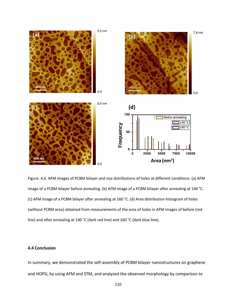
110
Figure. 4.6. AFM images of PCBM bilayer and size distributions of holes at different conditions. (a) AFM
image of a PCBM bilayer before annealing. (b) AFM image of a PCBM bilayer after annealing at 140 °C.
(c) AFM image of a PCBM bilayer after annealing at 160 °C. (d) Area distribution histogram of holes
(without PCBM area) obtained from measurements of the area of holes in AFM images of before (red
line) and after annealing at 140 °C (dark red line) and 160 °C (dark blue line).
4.4 Conclusion
In summary, we demonstrated the self-assembly of PCBM bilayer nanostructures on graphene
and HOPG, by using AFM and STM, and analyzed the observed morphology by comparison to
111
molecular models. The PCBM bilayer revealed two distinct configurations on HOPG with
different heights, and only one configuration on graphene. Post thermal annealing can induce
merging of the bilayer nanostructures. Our results will shed light on improvement of the energy
efficiency in solar cells containing graphene and organic molecules, by increasing the donor-
acceptor interface area.
References:
1. Li, Y. L.; Chen, C. H.; Burton, J.; Park, K.; Heflin, J. R.; Tao, C. G., Self-assembled PCBM bilayers on graphene and HOPG examined by AFM and STM. Nanotechnology 2018, 29 (18). 2. Meng, L. X.; Zhang, Y. M.; Wan, X. J.; Li, C. X.; Zhang, X.; Wang, Y. B.; Ke, X.; Xiao, Z.; Ding, L. M.; Xia, R. X.; Yip, H. L.; Cao, Y.; Chen, Y. S., Organic and solution-processed tandem solar cells with 17.3% efficiency. Science 2018, 361 (6407), 1094-+. 3. Zhao, W. C.; Li, S. S.; Yao, H. F.; Zhang, S. Q.; Zhang, Y.; Yang, B.; Hou, J. H., Molecular Optimization Enables over 13% Efficiency in Organic Solar Cells. J Am Chem Soc 2017, 139 (21), 7148-7151. 4. Xiao, Z.; Jia, X.; Ding, L. M., Ternary organic solar cells offer 14% power conversion efficiency. Sci Bull 2017, 62 (23), 1562-1564. 5. Cui, Y.; Yao, H. F.; Gao, B. W.; Qin, Y. P.; Zhang, S. Q.; Yang, B.; He, C.; Xu, B. W.; Hou, J. H., Fine-Tuned Photoactive and Interconnection Layers for Achieving over 13% Efficiency in a Fullerene-Free Tandem Organic Solar Cell. J Am Chem Soc 2017, 139 (21), 7302-7309. 6. Hoppe, H.; Sariciftci, N. S., Organic solar cells: An overview. J Mater Res 2004, 19 (7), 1924-1945. 7. Sariciftci, N. S.; Smilowitz, L.; Heeger, A. J.; Wudl, F., Photoinduced Electron-Transfer from a Conducting Polymer to Buckminsterfullerene. Science 1992, 258 (5087), 1474-1476. 8. Bagher, A. M., Introduction to organic solar cells Sustain. Energy 2014, 2, 85–90. 9. Gunes, S.; Neugebauer, H.; Sariciftci, N. S., Conjugated polymer-based organic solar cells. Chem Rev 2007, 107 (4), 1324-1338. 10. Scharber, M. C.; Wuhlbacher, D.; Koppe, M.; Denk, P.; Waldauf, C.; Heeger, A. J.; Brabec, C. L., Design rules for donors in bulk-heterojunction solar cells - Towards 10 % energy-conversion efficiency. Adv Mater 2006, 18 (6), 789-+. 11. Wienk, M. M.; Kroon, J. M.; Verhees, W. J. H.; Knol, J.; Hummelen, J. C.; van Hal, P. A.; Janssen, R. A. J., Efficient methano[70]fullerene/MDMO-PPV bulk heterojunction photovoltaic cells. Angew Chem Int Edit 2003, 42 (29), 3371-3375. 12. Liang, Y. Y.; Xu, Z.; Xia, J. B.; Tsai, S. T.; Wu, Y.; Li, G.; Ray, C.; Yu, L. P., For the Bright Future-Bulk Heterojunction Polymer Solar Cells with Power Conversion Efficiency of 7.4%. Adv Mater 2010, 22 (20), E135-+. 13. Padinger, F.; Rittberger, R. S.; Sariciftci, N. S., Effects of postproduction treatment on plastic solar cells. Adv Funct Mater 2003, 13 (1), 85-88.
112
14. Muhlbacher, D.; Scharber, M.; Morana, M.; Zhu, Z. G.; Waller, D.; Gaudiana, R.; Brabec, C., High photovoltaic performance of a low-bandgap polymer. Adv Mater 2006, 18 (21), 2884-+. 15. Li, G.; Shrotriya, V.; Yao, Y.; Yang, Y., Investigation of annealing effects and film thickness dependence of polymer solar cells based on poly(3-hexylthiophene). J Appl Phys 2005, 98 (4). 16. Ma, W. L.; Yang, C. Y.; Gong, X.; Lee, K.; Heeger, A. J., Thermally stable, efficient polymer solar cells with nanoscale control of the interpenetrating network morphology. Adv Funct Mater 2005, 15 (10), 1617-1622. 17. Wei, G. D.; Wang, S. Y.; Sun, K.; Thompson, M. E.; Forrest, S. R., Solvent-Annealed Crystalline Squaraine: PC70BM (1:6) Solar Cells. Adv Energy Mater 2011, 1 (2), 184-187. 18. Dang, M. T.; Hirsch, L.; Wantz, G., P3HT:PCBM, Best Seller in Polymer Photovoltaic Research. Adv Mater 2011, 23 (31), 3597-3602. 19. Bonaccorso, F.; Colombo, L.; Yu, G. H.; Stoller, M.; Tozzini, V.; Ferrari, A. C.; Ruoff, R. S.; Pellegrini, V., Graphene, related two-dimensional crystals, and hybrid systems for energy conversion and storage. Science 2015, 347 (6217). 20. Quesnel, E.; Roux, F.; Emieux, F.; Faucherand, P.; Kymakis, E.; Volonakis, G.; Giustino, F.; Martin-Garcia, B.; Moreels, I.; Gursel, S. A.; Yurtcan, A. B.; Di Noto, V.; Talyzin, A.; Baburin, I.; Tranca, D.; Seifert, G.; Crema, L.; Speranza, G.; Tozzini, V.; Bondavalli, P.; Pognon, G.; Botas, C.; Carriazo, D.; Singh, G.; Rojo, T.; Kim, G.; Yu, W. J.; Grey, C. P.; Pellegrini, V., Graphene-based technologies for energy applications, challenges and perspectives. 2d Mater 2015, 2 (3). 21. Zhang, Y. Y.; Hu, J. P.; Bernevig, B. A.; Wang, X. R.; Xie, X. C.; Liu, W. M., Localization and the Kosterlitz-Thouless Transition in Disordered Graphene. Phys Rev Lett 2009, 102 (10). 22. Hong, W. J.; Xu, Y. X.; Lu, G. W.; Li, C.; Shi, G. Q., Transparent graphene/PEDOT-PSS composite films as counter electrodes of dye-sensitized solar cells. Electrochem Commun 2008, 10 (10), 1555-1558. 23. Lee, Y. Y.; Tu, K. H.; Yu, C. C.; Li, S. S.; Hwang, J. Y.; Lin, C. C.; Chen, K. H.; Chen, L. C.; Chen, H. L.; Chen, C. W., Top Laminated Graphene Electrode in a Semitransparent Polymer Solar Cell by Simultaneous Thermal Annealing/Releasing Method. Acs Nano 2011, 5 (8), 6564-6570. 24. Wang, X.; Zhi, L. J.; Mullen, K., Transparent, conductive graphene electrodes for dye-sensitized solar cells. Nano Lett 2008, 8 (1), 323-327. 25. Wu, J. B.; Becerril, H. A.; Bao, Z. N.; Liu, Z. F.; Chen, Y. S.; Peumans, P., Organic solar cells with solution-processed graphene transparent electrodes. Appl Phys Lett 2008, 92 (26). 26. Takeuchi, O.; Takeuchi, N.; Ochiai, T.; Kato, H.; Yoshida, S.; Shigekawa, H., Microscopic description of the current-voltage characteristics of a bulk-heterojunction organic solar cell under illumination. Appl Phys Express 2014, 7 (2). 27. Chen, D. A.; Nakahara, A.; Wei, D. G.; Nordlund, D.; Russell, T. P., P3HT/PCBM Bulk Heterojunction Organic Photovoltaics: Correlating Efficiency and Morphology. Nano Lett 2011, 11 (2), 561-567. 28. Vanlaeke, P.; Swinnen, A.; Haeldermans, I.; Vanhoyland, G.; Aernouts, T.; Cheyns, D.; Deibel, C.; D'Haen, J.; Heremans, P.; Poortmans, J.; Manca, J. V., P3HT/PCBM bulk heterojunction solar cells: Relation between morphology and electro-optical characteristics. Sol Energ Mat Sol C 2006, 90 (14), 2150-2158. 29. Peet, J.; Kim, J. Y.; Coates, N. E.; Ma, W. L.; Moses, D.; Heeger, A. J.; Bazan, G. C., Efficiency enhancement in low-bandgap polymer solar cells by processing with alkane dithiols. Nat Mater 2007, 6 (7), 497-500. 30. Otero, R.; Ecija, D.; Fernandez, G.; Gallego, J. M.; Sanchez, L.; Martin, N.; Miranda, R., An organic donor/acceptor lateral superlattice at the nanoscale. Nano Lett 2007, 7 (9), 2602-2607. 31. Masui, A.; Sakaue, H.; Takahagi, T.; Suzuki, H., Intermixing behaviors of PCBM with CuPc on Au(111) surface. Chem Phys Lett 2016, 661, 215-218.
113
32. Gallego, J. M.; Ecija, D.; Martin, N.; Otero, R.; Miranda, R., An STM study of molecular exchange processes in organic thin film growth. Chem Commun 2014, 50 (69), 9954-9957. 33. Shao, Q.; Tskipuri, L.; Reutt-Robey, J. E., Vertical Phase Separation in Bilayer [6,6]-Phenyl-C-61-butyric Acid Methyl Ester:Zinc Phthalocyanine Films. J Phys Chem C 2014, 118 (32), 18612-18617. 34. Zheng, L. D.; Liu, J. G.; Han, Y. C., Polymer-regulated epitaxial crystallization of methanofullerene on mica. Phys Chem Chem Phys 2013, 15 (4), 1208-1215. 35. Hoppe, H.; Sariciftci, N. S., Morphology of polymer/fullerene bulk heterojunction solar cells. J Mater Chem 2006, 16 (1), 45-61. 36. Jin, Z. W.; Wang, J. Z., PIN architecture for ultrasensitive organic thin film photoconductors. Sci Rep-Uk 2014, 4. 37. Pratihar, P.; Ghosh, S.; Stepanenko, V.; Patwardhan, S.; Grozema, F. C.; Siebbeles, L. D. A.; Wurthner, F., Self-assembly and semiconductivity of an oligothiophene supergelator. Beilstein J Org Chem 2010, 6, 1070-1078. 38. Ji, A. C.; Xie, X. C.; Liu, W. M., Quantum magnetic dynamics of polarized light in arrays of microcavities. Phys Rev Lett 2007, 99 (18). 39. Yang, X. N.; van Duren, J. K. J.; Rispens, M. T.; Hummelen, J. C.; Janssen, R. A. J.; Michels, M. A. J.; Loos, J., Crystalline organization of a methanofullerene as used for plastic solar-cell applications. Adv Mater 2004, 16 (9-10), 802-+. 40. Tskipuri, L.; Shao, Q.; Reutt-Robey, J., Molecular Ordering in PCBM-Au(111) Interface Formation. J Phys Chem C 2012, 116 (41), 21874-21879. 41. Ecija, D.; Otero, R.; Sanchez, L.; Gallego, J. M.; Wang, Y.; Alcami, M.; Martin, F.; Martin, N.; Miranda, R., Crossover site-selectivity in the adsorption of the fullerene derivative PCBM on Au(111). Angew Chem Int Edit 2007, 46 (41), 7874-7877. 42. Li, H.; Duan, Y. Q.; Coropceanu, V.; Bredas, J. L., Electronic structure of the pentacene-gold interface: A density-functional theory study. Org Electron 2009, 10 (8), 1571-1578. 43. Huebener, K.; Scheloske, M.; Hauschild, J.; Harneit, W.; Zehl, G.; Fiechter, S., AFM investigation of the formation of one-dimensional structures of C(60) shuttlecocks on HOPG. Phys Status Solidi B 2006, 243 (13), 2990-2994. 44. Walczyk, W.; Schon, P. M.; Schonherr, H., The effect of PeakForce tapping mode AFM imaging on the apparent shape of surface nanobubbles. J Phys-Condens Mat 2013, 25 (18). 45. Girard, C.; Lambin, P.; Dereux, A.; Lucas, A. A., Van-Der-Waals Attraction between 2 C60 Fullerene Molecules and Physical Adsorption of C60 on Graphite and Other Substrates. Phys Rev B 1994, 49 (16), 11425-11432. 46. Wang, Y.; Alcami, M.; Martin, F., Understanding the supramolecular self-assembly of the fullerene derivative PCBM on gold surfaces. Chemphyschem 2008, 9 (7), 1030-1035. 47. Girifalco, L. A.; Hodak, M.; Lee, R. S., Carbon nanotubes, buckyballs, ropes, and a universal graphitic potential. Phys Rev B 2000, 62 (19), 13104-13110. 48. Branz, W.; Malinowski, N.; Enders, A.; Martin, T. P., Structural transition in (C-60)(n) clusters. Phys Rev B 2002, 66 (9). 49. Wang, C. I.; Hua, C. C., Solubility of C-60 and PCBM in Organic Solvents. J Phys Chem B 2015, 119 (45), 14496-14504. 50. Gravil, P. A.; Devel, M.; Lambin, P.; Bouju, X.; Girard, C.; Lucas, A. A., Adsorption of C-60 molecules. Phys Rev B 1996, 53 (3), 1622-1629. 51. Igathinathane, C.; Pordesimo, L. O.; Columbus, E. P.; Batchelor, W. D.; Methuku, S. R., Shape identification and particles size distribution from basic shape parameters using ImageJ. Comput Electron Agr 2008, 63 (2), 168-182. 52. Scott, D. W., Optimal and Data-Based Histograms. Biometrika 1979, 66 (3), 605-610.
114 This chapter closely follows the publication: Li, Y.; Liu, X.; Chen, C.; Duchamp, J.; Huang, R.; Chung, T.; Young, M.; Chalal, T.; Chen, Y.P.; Heflin, J.R.; Dorn, H.; Tao, C., Differences in Self-Assembly of Spherical C60 and Planar PTCDA on Rippled Graphene Surfaces, Carbon 145, 549 (2019)
Chapter 5
Differences in Self-Assembly of Spherical C60 and Planar
PTCDA on Rippled Graphene Surfaces
The majority of this chapter is from a manuscript published in Carbon, with slight modifications.
The experimental part of this chapter is done by Yanlong Li with the help of Chuanhui Chen. The
DFT calculation part is due to the work of Xiaoyang Liu.
5.1 Introduction
Graphene is a unique two-dimensional (2D) material that exhibits fascinating physical and
chemical properties and has a wide range of applications.1-3 For instance, thanks to its single-
atom thickness and flexibility, graphene is an excellent candidate for flexible electronics and gas
sensors.4-9 To optimize the applications of graphene and other 2D materials, it is essential to
investigate how curvature affects and tunes their properties. It has been reported that
graphene on rough substrates (e.g. SiO2) or suspended exhibits nonplanar aberrations.10-11
Furthermore, rippling the graphene to induce a curved surface would introduce variability into
the properties of graphene and changes interactions with adsorbed molecules, which has not
been experimentally examined.
Significant research efforts have recently been devoted to investigate the adsorption and
desorption of various molecules on planar graphene and other 2D materials, such as fabricating
115
and tuning molecule/graphene hybrid structures.12-16 Among the organic species, C60 and
perylenetetracarboxylic dianhydride (PTCDA) have attracted a huge amount of research
interest partially because they are key components, as effective electron acceptors, in
photovoltaic cells.12, 16-24 In the past two decades, the power conversion efficiency of organic
solar cells has rapidly increased, currently beyond 17%.25 To further improve the efficiency of
organic cells, it is necessary to understand the interactions between the organic species and
other building blocks like graphene, which is an excellent material for transparent electrodes in
solar cells.26-27 Development and study of hybrid nanostructures based on rippled graphene,
C60/rippled graphene, and PTCDA/rippled graphene could provide significant insights for
improving the efficiency of organic solar cells.
Previous experimental and computational studies have found that C60 and PTCDA on a planar
graphene surface form a hexagonal close packed (hcp) structure and a herringbone structure,
respectively.12-13, 16-19, 28-29 The major interaction present in the C60-planar graphene system is a
π-π stacking interaction.30 π-π stacking interactions are common in parallel aromatic systems,
have distances ranging from 3.0 to 4.0 Å and are mainly based on van der Waals forces.31-32 The
PTCDA-graphene system also contains π-π stacking interactions, but the dominant interaction
that leads to a herringbone pattern is intermolecular hydrogen bonding.17 We here report
significant experimental and computational differences of spherical C60 and planar PTCDA self-
assembled structures on rippled graphene surfaces. The inherent ability to tune the
interactions between rippled graphene and structurally different molecules will undoubtedly
open the door to interesting properties and potential applications of curved 2D materials, such
as flexible sensors.33-36
116
5.2 Experimental and Computational Methods
Experimental: All STM measurements were carried out in an ultra-high vacuum (UHV) scanning
tunneling microscope system (Omicron RT-STM). Before C60 deposition, the graphene was
grown using chemical vapor deposition (CVD) onto Cu foil37 and annealed for 12 hours at 673K
in a preparation chamber with a base pressure of 1 x 10⁻¹⁰ torr. PTCDA powder (TCI AMERICA,
99.0% purity) was loaded into the homemade Knudsen cell and mounted in the load lock side A
of the STM system. C60 powder (MER Corporation, 99.5% purity) was loaded into the
homemade Knudsen cell and mounted in the load lock side B of the STM system. The C60 and
PTCDA sources were degassed to 1 x 10⁻⁶ torr prior to deposition. C60 and PTCDA molecules
were then simultaneously deposited onto a same graphene at a deposition rate of ~ 0.5
monolayer/min with the background pressure below 1.8×10⁻⁸ torr. During the deposition
process, the substrate was kept at 413 K. The sample was subsequently annealed at 423 K for
one hour in the preparation chamber of the STM system with a base pressure of 1.0 x 10⁻¹⁰ torr.
All of the STM measurements were performed at room temperature with a base pressure of 1.9
× 10-10 torr. The STM used a chemically etched tungsten tip.
Computational: My collaborator Xiaoyang Liu does this computational part. Density functional
theory (DFT) based calculations are used to obtain further understanding of the self-assembled
systems. A model containing an adsorbed molecule and a curved graphene surface is used to
simulate the attachment of C60 and PTCDA on the rippled graphene surface. The structures of
C60 and PTCDA are fully optimized at the B3LYP level with def2-SVP basis set as provided in
ORCA 3.0.3. The curved graphene is constructed based on experiment observation and then is
optimized with constraints to maintain the bending angles and size. The energies of the
117
combined system are estimated based on single point calculations.38-40 DFT based approaches
with D3-correction are used to address the intermolecular interactions between the C60/PTCDA
molecules and the graphene.41-42 The distance between C60 and the curved graphene surface
are changed consistently and the system energy for each distance is calculated. The energy of
the C60- curved graphene complex is sensitive to the orientation of the C60 molecules on
graphene. To solve the orientation-related challenge, we employed a detailed minimum
potential search on representative orientations.43-44 Comparative calculations with molecules
adsorbed on planar graphene are also reported.
5.3 Discussions
The self-assembled structure of molecules adsorbed on graphene relates to the geometry of
graphene underneath. We identified three different patterns of graphene: planar graphene
labeled as I (Figures 5.1h and i)), one-dimensional (1D)-rippled graphene labeled as II (Figures
5.1a-d), 2D-rippled graphene labeled as III (Figures 5.1e and f). Planar graphene usually forms a
moiré pattern on Cu substrate. Figure 5.1i shows a moiré pattern with a hexagonal moiré super
lattice with periodicity of 2.0 nm. Besides the planar graphene areas, we also observed 1D-
rippled graphene (Figure 5.1a-c). Figure 5.1a shows the coexistence of planar graphene (I) and
1D-rippled graphene (II). Figure 5.1d, a line profile of the blue line in Figure 5.1b, shows a
periodicity of ~5 nm with amplitude of 0.23 nm. Typically, the peaks of the rippled graphene
have heights that range from 0.2 nm to 0.4 nm and periodicities that range from 3 nm to 10
nm. High resolution STM images (Figure 5.1c and Figure 5.2d and e) reveal a honeycomb lattice
118
of graphene on the top of each ripple. For 2D-rippled graphene (Figures 5.1e and f), the ripples
are along two perpendicular directions with the peak height and periodicity similar to 1D-
rippled graphene. Considering the heights of the ripples are much higher than the surface
smoothness of the underneath Cu(111), Cu(100) or Cu(110) that is in the range of less than 0.1
nm,34, 45 the line profiles of the ripples (Figure 5.2 b, c) indicate that the graphene in these areas
is quasi-suspended over the Cu substrate.
Figure 5.1. STM topographical images of planar graphene (labeled as I), 1D-rippled graphene (II) and 2D-
rippled graphene (III) on Cu. (a) Large area STM image of planar graphene (I) and 1D-rippled graphene
(II) showing the linear periodic modulation and the spatial modulation frequencies (Vs = -2.340 V, I =
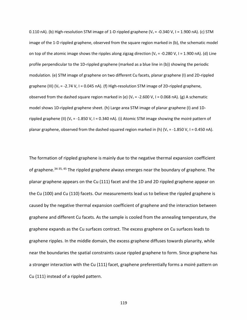
119
0.110 nA). (b) High-resolution STM image of 1-D rippled graphene (Vs = -0.340 V, I = 1.900 nA). (c) STM
image of the 1-D rippled graphene, observed from the square region marked in (b), the schematic model
on top of the atomic image shows the ripples along zigzag direction (Vs = -0.280 V, I = 1.900 nA). (d) Line
profile perpendicular to the 1D-rippled graphene (marked as a blue line in (b)) showing the periodic
modulation. (e) STM image of graphene on two different Cu facets, planar graphene (I) and 2D-rippled
graphene (III) (Vs = -2.74 V, I = 0.045 nA). (f) High-resolution STM image of 2D-rippled graphene,
observed from the dashed square region marked in (e) (Vs = -2.600 V, I = 0.068 nA). (g) A schematic
model shows 1D-rippled graphene sheet. (h) Large area STM image of planar graphene (I) and 1D-
rippled graphene (II) (Vs = -1.850 V, I = 0.340 nA). (i) Atomic STM image showing the moiré pattern of
planar graphene, observed from the dashed squared region marked in (h) (Vs = -1.850 V, I = 0.450 nA).
The formation of rippled graphene is mainly due to the negative thermal expansion coefficient
of graphene.34-35, 45 The rippled graphene always emerges near the boundary of graphene. The
planar graphene appears on the Cu (111) facet and the 1D and 2D rippled graphene appear on
the Cu (100) and Cu (110) facets. Our measurements lead us to believe the rippled graphene is
caused by the negative thermal expansion coefficient of graphene and the interaction between
graphene and different Cu facets. As the sample is cooled from the annealing temperature, the
graphene expands as the Cu surfaces contract. The excess graphene on Cu surfaces leads to
graphene ripples. In the middle domain, the excess graphene diffuses towards planarity, while
near the boundaries the spatial constraints cause rippled graphene to form. Since graphene has
a stronger interaction with the Cu (111) facet, graphene preferentially forms a moiré pattern on
Cu (111) instead of a rippled pattern.
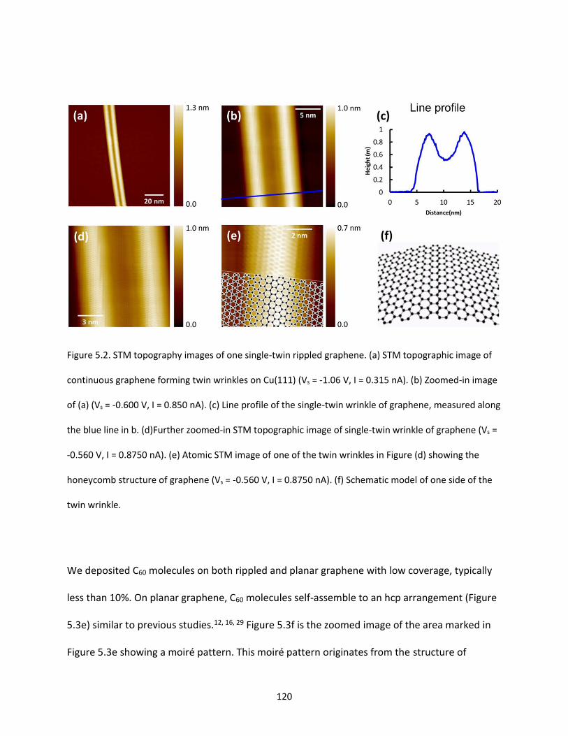
120
Figure 5.2. STM topography images of one single-twin rippled graphene. (a) STM topographic image of
continuous graphene forming twin wrinkles on Cu(111) (Vs = -1.06 V, I = 0.315 nA). (b) Zoomed-in image
of (a) (Vs = -0.600 V, I = 0.850 nA). (c) Line profile of the single-twin wrinkle of graphene, measured along
the blue line in b. (d)Further zoomed-in STM topographic image of single-twin wrinkle of graphene (Vs =
-0.560 V, I = 0.8750 nA). (e) Atomic STM image of one of the twin wrinkles in Figure (d) showing the
honeycomb structure of graphene (Vs = -0.560 V, I = 0.8750 nA). (f) Schematic model of one side of the
twin wrinkle.
We deposited C60 molecules on both rippled and planar graphene with low coverage, typically
less than 10%. On planar graphene, C60 molecules self-assemble to an hcp arrangement (Figure
5.3e) similar to previous studies.12, 16, 29 Figure 5.3f is the zoomed image of the area marked in
Figure 5.3e showing a moiré pattern. This moiré pattern originates from the structure of

121
graphene and the Cu (111) surface as shown in Figure 5.1i. For C60 on rippled graphene, the C60
self-assembly is more complicated than that on the planar case. C60 molecules form a quasi-hcp
structure as shown in Figures 5.3a-c at various scales. The quasi-hcp structure formed on
rippled graphene has a different angle from that formed on the planar area. For example, the
angle shown in Figure 5.3c is 54.1o instead of 60.0o shown in Figure 5.3f. The angle difference
between C60 on rippled graphene and planar graphene is due to the geometric curvature of the
rippled graphene. When compared to C60 adsorbed on planar graphene, the hcp structure on
rippled graphene is distorted by the curvature of the surface. The difference is also reflected in
the corresponding Fast Fourier Transform (FFT) images (the insets in Figures 5.3c and e).
Figure 5.3. STM images of C60 on 1D-rippled graphene (II) and on planar graphene (I). (a) Large area STM
topographic image of the C60 on 1D-rippled graphene showing well-defined linear periodic modulated
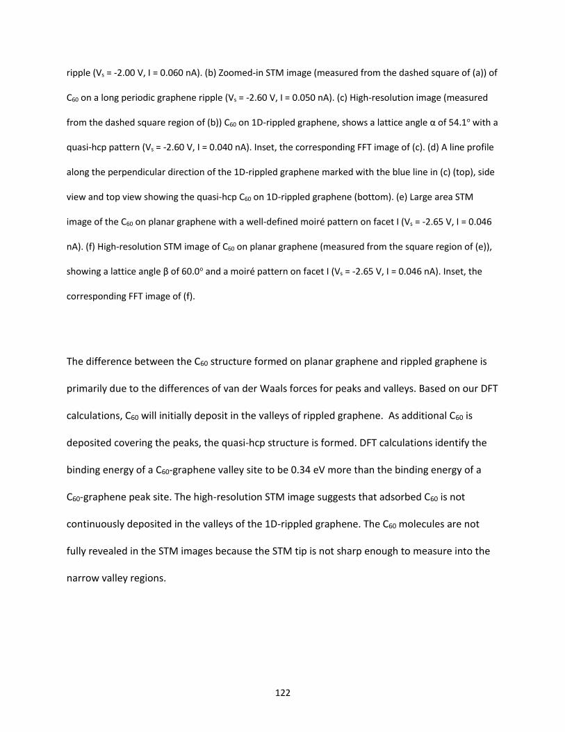
122
ripple (Vs = -2.00 V, I = 0.060 nA). (b) Zoomed-in STM image (measured from the dashed square of (a)) of
C60 on a long periodic graphene ripple (Vs = -2.60 V, I = 0.050 nA). (c) High-resolution image (measured
from the dashed square region of (b)) C60 on 1D-rippled graphene, shows a lattice angle α of 54.1o with a
quasi-hcp pattern (Vs = -2.60 V, I = 0.040 nA). Inset, the corresponding FFT image of (c). (d) A line profile
along the perpendicular direction of the 1D-rippled graphene marked with the blue line in (c) (top), side
view and top view showing the quasi-hcp C60 on 1D-rippled graphene (bottom). (e) Large area STM
image of the C60 on planar graphene with a well-defined moiré pattern on facet I (Vs = -2.65 V, I = 0.046
nA). (f) High-resolution STM image of C60 on planar graphene (measured from the square region of (e)),
showing a lattice angle β of 60.0o and a moiré pattern on facet I (Vs = -2.65 V, I = 0.046 nA). Inset, the
corresponding FFT image of (f).
The difference between the C60 structure formed on planar graphene and rippled graphene is
primarily due to the differences of van der Waals forces for peaks and valleys. Based on our DFT
calculations, C60 will initially deposit in the valleys of rippled graphene. As additional C60 is
deposited covering the peaks, the quasi-hcp structure is formed. DFT calculations identify the
binding energy of a C60-graphene valley site to be 0.34 eV more than the binding energy of a
C60-graphene peak site. The high-resolution STM image suggests that adsorbed C60 is not
continuously deposited in the valleys of the 1D-rippled graphene. The C60 molecules are not
fully revealed in the STM images because the STM tip is not sharp enough to measure into the
narrow valley regions.
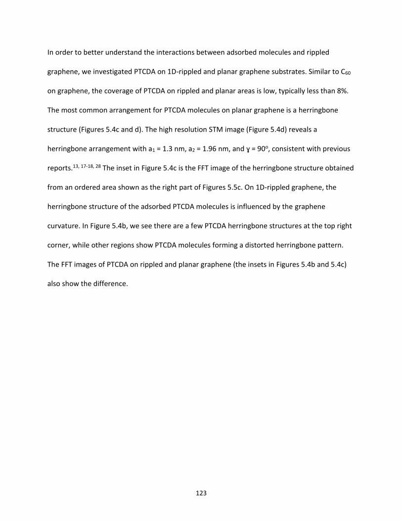
123
In order to better understand the interactions between adsorbed molecules and rippled
graphene, we investigated PTCDA on 1D-rippled and planar graphene substrates. Similar to C60
on graphene, the coverage of PTCDA on rippled and planar areas is low, typically less than 8%.
The most common arrangement for PTCDA molecules on planar graphene is a herringbone
structure (Figures 5.4c and d). The high resolution STM image (Figure 5.4d) reveals a
herringbone arrangement with a1 = 1.3 nm, a2 = 1.96 nm, and ɣ = 90o, consistent with previous
reports.13, 17-18, 28 The inset in Figure 5.4c is the FFT image of the herringbone structure obtained
from an ordered area shown as the right part of Figures 5.5c. On 1D-rippled graphene, the
herringbone structure of the adsorbed PTCDA molecules is influenced by the graphene
curvature. In Figure 5.4b, we see there are a few PTCDA herringbone structures at the top right
corner, while other regions show PTCDA molecules forming a distorted herringbone pattern.
The FFT images of PTCDA on rippled and planar graphene (the insets in Figures 5.4b and 5.4c)
also show the difference.
124
Figure. 5.4. STM images of PTCDA on 1D-rippled graphene and on planar graphene. (a) Large area STM
image of PTCDA on 1D-rippled graphene (Vs = -2.51 V, I = 0.042 nA). (b) STM image of PTCDA on 1D-
rippled graphene showing a distorted herringbone pattern (Vs = -2.510 V, I = 0.042 nA). Inset, the
corresponding FFT image of (b). (c) Large area STM image of PTCDA on planar graphene (Vs = 1.800 V, I =
0.030 nA). Inset, the FFT image of the PTCDA herringbone structure on planar graphene. (d) Zoomed-in
STM image of PTCDA on planar graphene; a1 and a2 indicate the short and long lattice vectors of a unit
cell of the PTCDA herringbone pattern (Vs = 1.800 V, I = 0.030 nA). (e) STM images of coexistence of
substable PTCDA structure (purple curved region) and normal PTCDA herringbone structure (Vs = -2.500
V, I = 0.030 nA). (f) STM image of remaining normal PTCDA structure after the substable PTCDA was
removed by STM tip (Vs = -2.500 V, I = 0.030 nA).
Our results (Figures 5.4e, f and Figure 5.5) further show that PTCDA sub monolayer is very easy
to disassemble, due to the weak interaction between the PTCDA molecule and graphene on
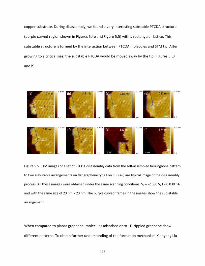
125
copper substrate. During disassembly, we found a very interesting substable PTCDA structure
(purple curved region shown in Figures 5.4e and Figure 5.5) with a rectangular lattice. This
substable structure is formed by the interaction between PTCDA molecules and STM tip. After
growing to a critical size, the substable PTCDA would be moved away by the tip (Figures 5.5g
and h).
Figure 5.5. STM images of a set of PTCDA disassembly data from the self-assembled herringbone pattern
to two sub-stable arrangements on flat graphene type I on Cu. (a-i) are typical image of the disassembly
process. All these images were obtained under the same scanning conditions: Vs = -2.500 V, I = 0.030 nA,
and with the same size of 23 nm × 23 nm. The purple curved frames in the images show the sub-stable
arrangement.
When compared to planar graphene, molecules adsorbed onto 1D-rippled graphene show
different patterns. To obtain further understanding of the formation mechanism Xiaoyang Liu
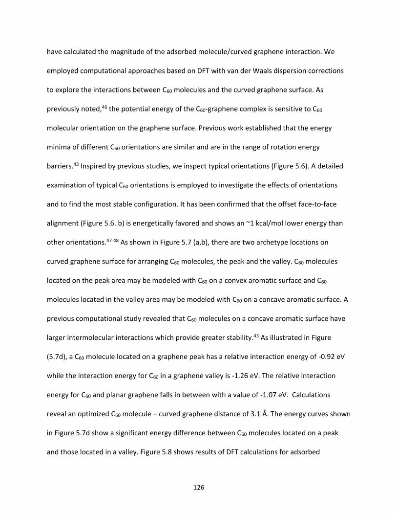
126
have calculated the magnitude of the adsorbed molecule/curved graphene interaction. We
employed computational approaches based on DFT with van der Waals dispersion corrections
to explore the interactions between C60 molecules and the curved graphene surface. As
previously noted,46 the potential energy of the C60-graphene complex is sensitive to C60
molecular orientation on the graphene surface. Previous work established that the energy
minima of different C60 orientations are similar and are in the range of rotation energy
barriers.43 Inspired by previous studies, we inspect typical orientations (Figure 5.6). A detailed
examination of typical C60 orientations is employed to investigate the effects of orientations
and to find the most stable configuration. It has been confirmed that the offset face-to-face
alignment (Figure 5.6. b) is energetically favored and shows an ~1 kcal/mol lower energy than
other orientations.47-48 As shown in Figure 5.7 (a,b), there are two archetype locations on
curved graphene surface for arranging C60 molecules, the peak and the valley. C60 molecules
located on the peak area may be modeled with C60 on a convex aromatic surface and C60
molecules located in the valley area may be modeled with C60 on a concave aromatic surface. A
previous computational study revealed that C60 molecules on a concave aromatic surface have
larger intermolecular interactions which provide greater stability.43 As illustrated in Figure
(5.7d), a C60 molecule located on a graphene peak has a relative interaction energy of -0.92 eV
while the interaction energy for C60 in a graphene valley is -1.26 eV. The relative interaction
energy for C60 and planar graphene falls in between with a value of -1.07 eV. Calculations
reveal an optimized C60 molecule – curved graphene distance of 3.1 Å. The energy curves shown
in Figure 5.7d show a significant energy difference between C60 molecules located on a peak
and those located in a valley. Figure 5.8 shows results of DFT calculations for adsorbed
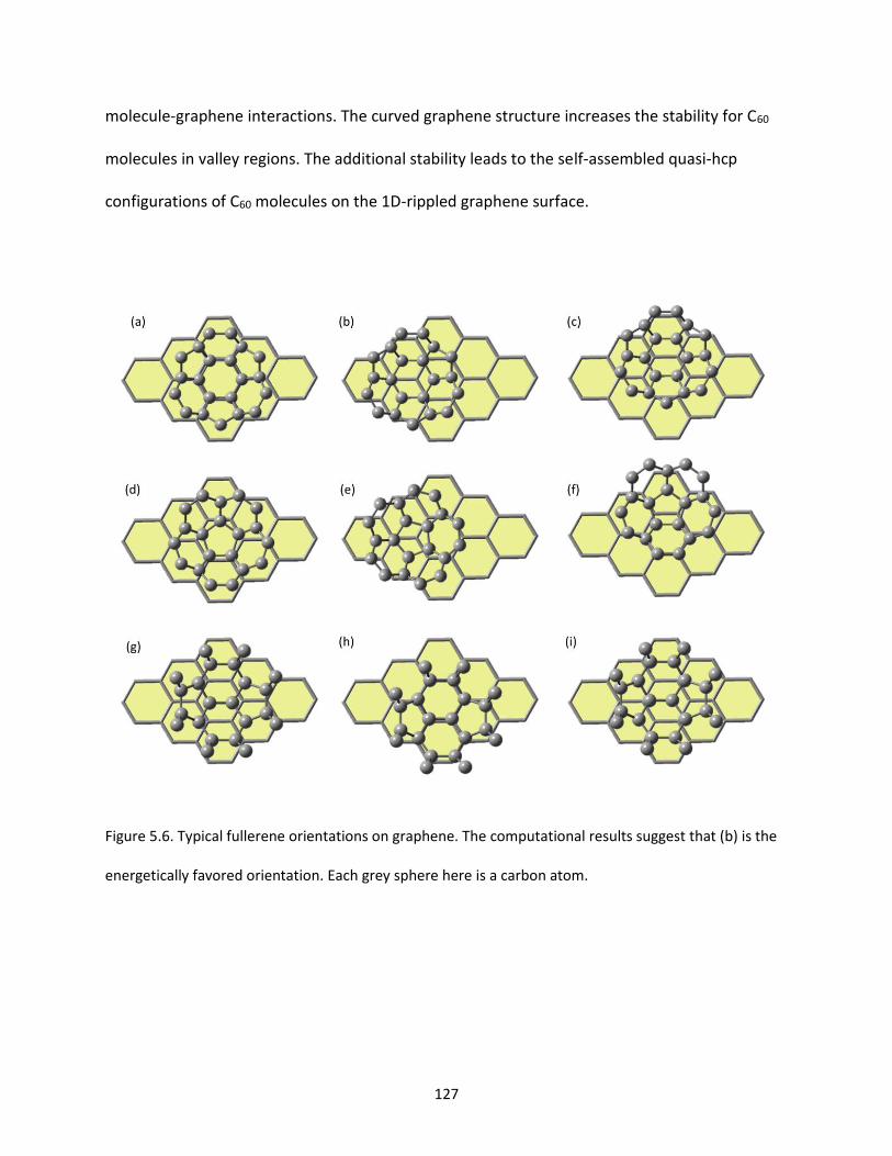
127
molecule-graphene interactions. The curved graphene structure increases the stability for C60
molecules in valley regions. The additional stability leads to the self-assembled quasi-hcp
configurations of C60 molecules on the 1D-rippled graphene surface.
Figure 5.6. Typical fullerene orientations on graphene. The computational results suggest that (b) is the
energetically favored orientation. Each grey sphere here is a carbon atom.
128
Figure 5.7. Computational results for C60 on 1D-rippled graphene and planar graphene showing
energetically favored orientations. (a) C60 molecule on a peak site on curved-graphene, (b) C60 molecule
with a valley site on curved-graphene and (c) C60 on planar-graphene. (d) Plot of C60-graphene distance
versus relative energy for C60 on a graphene peak (pink), C60 in a graphene valley (blue) and C60 on planar
graphene (green).
In contrast to the hcp pattern for C60 molecules on a planar graphene surface, it has been
shown that PTCDA molecules form herringbone structure on a planar graphene surface.
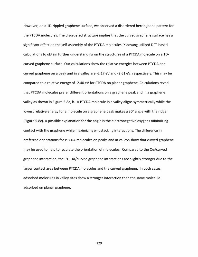
129
However, on a 1D-rippled graphene surface, we observed a disordered herringbone pattern for
the PTCDA molecules. The disordered structure implies that the curved graphene surface has a
significant effect on the self-assembly of the PTCDA molecules. Xiaoyang utilized DFT-based
calculations to obtain further understanding on the structures of a PTCDA molecule on a 1D-
curved graphene surface. Our calculations show the relative energies between PTCDA and
curved graphene on a peak and in a valley are -2.17 eV and -2.61 eV, respectively. This may be
compared to a relative energy of -2.40 eV for PTCDA on planar graphene. Calculations reveal
that PTCDA molecules prefer different orientations on a graphene peak and in a graphene
valley as shown in Figure 5.8a, b. A PTCDA molecule in a valley aligns symmetrically while the
lowest relative energy for a molecule on a graphene peak makes a 30˚ angle with the ridge
(Figure 5.8c). A possible explanation for the angle is the electronegative oxygens minimizing
contact with the graphene while maximizing π-π stacking interactions. The difference in
preferred orientations for PTCDA molecules on peaks and in valleys show that curved graphene
may be used to help to regulate the orientation of molecules. Compared to the C60/curved
graphene interaction, the PTCDA/curved graphene interactions are slightly stronger due to the
larger contact area between PTCDA molecules and the curved graphene. In both cases,
adsorbed molecules in valley sites show a stronger interaction than the same molecule
adsorbed on planar graphene.
130
Figure 5.8. DFT results for adsorbed molecule/graphene interactions. (a) Energy difference of a C60
molecule on a 1D-rippled graphene surface (b) Energy difference of a PTCDA molecule on a 1D-rippled
graphene. (c) Energy curve for a PTCDA molecule rotation on 1D-rippled graphene on a peak location
(top). (d) Favored PTCDA orientations at the peak site (left) and at the valley site (right).
5.4 Conclusion
In this chapter, we have demonstrated the self-assembly of C60 and PTCDA molecules on rippled
graphene with characterization using both experimental STM and DFT calculations. The
adsorbed molecules on 1D-rippled graphene systems reveal distortions when compared with
the analogous planar graphene system. Specifically, the nearly spherical Ih-symmetrical C60
molecules form a quasi-hexagonal close packed structure, while the planar PTCDA molecules
form a disordered herringbone structure on the rippled graphene surface. The change in the
131
monolayer packing pattern of C60 and PTCDA molecules on a curved graphene surface is due to
competition between the adsorbate-graphene interaction and the intermolecular adsorbate
interactions. Because of the nearly spherical C60 molecules, the rippled graphene surface
exhibits only diminished effects on the π-π intermolecular interactions. In contrast, the planar
PTCDA molecules have different sides for intermolecular interactions, namely, sp2 hybridized on
opposite two sides and significantly more electronegative oxygen anhydride moieties on the
other two sides. This leads to the well characterized herringbone structure that is assembled
mainly based on the relative weak PTCDA hydrogen bonds, C-H…O, with a strength estimated
as 0.1 eV. In this case, the PTCDA-graphene interaction, which have energies at the peak and
valley sites of 2.17 and 2.61 eV, respectively, are far more important than the PTCDA
intermolecular interaction. These results are also consistent with the tendency for dissembling
the PTCDA submonolayer vide supra. Furthermore, the DFT computational results demonstrate
significant increases in π-π interactions for both the adsorbed PTCDA and C60/rippled graphene
complexes located in the 2D graphene valley sites in comparison with adsorbed more idealized
molecule/planar graphene 2D complexes. In addition, we find that the adsorbed planar PTCDA
molecules prefer different orientations when the rippled graphene peak regions are compared
to the valley regions. These fundamental experimental and computational results are important
for understanding any potential application of structurally diverse molecules adsorbed on
graphene and/or rippled graphene surfaces.
132
References:
1. Novoselov, K. S.; Geim, A. K.; Morozov, S. V.; Jiang, D.; Katsnelson, M. I.; Grigorieva, I. V.; Dubonos, S. V.; Firsov, A. A., Two-dimensional gas of massless Dirac fermions in graphene. Nature 2005, 438 (7065), 197-200. 2. Zhang, Y. B.; Tan, Y. W.; Stormer, H. L.; Kim, P., Experimental observation of the quantum Hall effect and Berry's phase in graphene. Nature 2005, 438 (7065), 201-204. 3. Castro Neto, A. H.; Guinea, F.; Peres, N. M. R.; Novoselov, K. S.; Geim, A. K., The electronic properties of graphene. Rev Mod Phys 2009, 81 (1), 109-162. 4. Georgiou, T.; Jalil, R.; Belle, B. D.; Britnell, L.; Gorbachev, R. V.; Morozov, S. V.; Kim, Y. J.; Gholinia, A.; Haigh, S. J.; Makarovsky, O.; Eaves, L.; Ponomarenko, L. A.; Geim, A. K.; Novoselov, K. S.; Mishchenko, A., Vertical field-effect transistor based on graphene-WS2 heterostructures for flexible and transparent electronics. Nat Nanotechnol 2013, 8 (2), 100-103. 5. Kim, Y. H.; Kim, S. J.; Kim, Y. J.; Shim, Y. S.; Kim, S. Y.; Hong, B. H.; Jang, H. W., Self-Activated Transparent All-Graphene Gas Sensor with Endurance to Humidity and Mechanical Bending. Acs Nano 2015, 9 (10), 10453-10460. 6. Sentef, M. A.; Claassen, M.; Kemper, A. F.; Moritz, B.; Oka, T.; Freericks, J. K.; Devereaux, T. P., Theory of Floquet band formation and local pseudospin textures in pump-probe photoemission of graphene. Nat Commun 2015, 6, 7047(1-8). 7. Geim, A. K., Graphene: Status and Prospects. Science 2009, 324 (5934), 1530-1534. 8. Zurutuza, A.; Marinelli, C., Challenges and opportunities in graphene commercialization. Nat Nanotechnol 2014, 9 (10), 730-734. 9. Avouris, P.; Xia, F. N., Graphene applications in electronics and photonics. Mrs Bull 2012, 37 (12), 1225-1234. 10. Bao, W. Z.; Miao, F.; Chen, Z.; Zhang, H.; Jang, W. Y.; Dames, C.; Lau, C. N., Controlled ripple texturing of suspended graphene and ultrathin graphite membranes. Nat Nanotechnol 2009, 4 (9), 562-566. 11. Ishigami, M.; Chen, J. H.; Cullen, W. G.; Fuhrer, M. S.; Williams, E. D., Atomic structure of graphene on SiO2. Nano Lett 2007, 7 (6), 1643-1648. 12. Li, G.; Zhou, H. T.; Pan, L. D.; Zhang, Y.; Mao, J. H.; Zou, Q.; Guo, H. M.; Wang, Y. L.; Du, S. X.; Gao, H. J., Self-assembly of C-60 monolayer on epitaxially grown, nanostructured graphene on Ru(0001) surface. Appl Phys Lett 2012, 100 (1), 013304(1-4). 13. Wang, Q. H.; Hersam, M. C., Room-temperature molecular-resolution characterization of self-assembled organic monolayers on epitaxial graphene. Nat Chem 2009, 1 (3), 206-211. 14. MacLeod, J. M.; Rosei, F., Molecular Self-Assembly on Graphene. Small 2014, 10 (6), 1038-1049. 15. Jarvinen, P.; Hamalainen, S. K.; Ijas, M.; Harju, A.; Liljeroth, P., Self-Assembly and Orbital Imaging of Metal Phthalocyanines on a Graphene Model Surface. J Phys Chem C 2014, 118 (24), 13320-13325. 16. Chen, C. H.; Zheng, H. S.; Mills, A.; Heflin, J. R.; Tao, C. G., Temperature Evolution of Quasi-one-dimensional C-60 Nanostructures on Rippled Graphene. Sci Rep-Uk 2015, 5, 14336(1-7). 17. Martinez-Galera, A. J.; Nicoara, N.; Martinez, J. I.; Dappe, Y. J.; Ortega, J.; Gomez-Rodriguez, J. M., Imaging Molecular Orbitals of PTCDA on Graphene on Pt(111): Electronic Structure by STM and First-Principles Calculations. J Phys Chem C 2014, 118 (24), 12782-12788. 18. Emery, J. D.; Wang, Q. H.; Zarrouati, M.; Fenter, P.; Hersam, M. C.; Bedzyk, M. J., Structural analysis of PTCDA monolayers on epitaxial graphene with ultra-high vacuum scanning tunneling microscopy and high-resolution X-ray reflectivity. Surf Sci 2011, 605 (17-18), 1685-1693. 19. Lu, J.; Yeo, P. S. E.; Zheng, Y.; Yang, Z. Y.; Bao, Q. L.; Gan, C. K.; Loh, K. P., Using the Graphene Moire Pattern for the Trapping of C-60 and Homoepitaxy of Graphene. Acs Nano 2012, 6 (1), 944-950.
133
20. Sariciftci, N. S.; Smilowitz, L.; Heeger, A. J.; Wudl, F., Photoinduced Electron-Transfer from a Conducting Polymer to Buckminsterfullerene. Science 1992, 258 (5087), 1474-1476. 21. Morita, S.; Zakhidov, A. A.; Yoshino, K., Doping Effect of Buckminsterfullerene in Conducting Polymer - Change of Absorption-Spectrum and Quenching of Luminescence. Solid State Commun 1992, 82 (4), 249-252. 22. Smilowitz, L.; Sariciftci, N. S.; Wu, R.; Gettinger, C.; Heeger, A. J.; Wudl, F., Photoexcitation Spectroscopy of Conducting-Polymer-C(60) Composites - Photoinduced Electron-Transfer. Phys Rev B 1993, 47 (20), 13835-13842. 23. Peumans, P.; Yakimov, A.; Forrest, S. R., Small molecular weight organic thin-film photodetectors and solar cells. J Appl Phys 2003, 93 (7), 3693-3723. 24. Rand, B. P.; Burk, D. P.; Forrest, S. R., Offset energies at organic semiconductor heterojunctions and their influence on the open-circuit voltage of thin-film solar cells. Phys Rev B 2007, 75 (11), 115327(1-11). 25. Meng, L.; Zhang, Y.; Wan, X.; Li, C.; Zhang, X.; Wang, Y.; Ke, X.; Xiao, Z.; Ding, L.; Xia, R.; Yip, H.-L.; Cao, Y.; Chen, Y., Organic and solution-processed tandem solar cells with 17.3% efficiency. Science 2018, 361 (6407), 1094-1098. 26. Wang, X.; Zhi, L. J.; Mullen, K., Transparent, conductive graphene electrodes for dye-sensitized solar cells. Nano Lett 2008, 8 (1), 323-327. 27. Wu, J. B.; Becerril, H. A.; Bao, Z. N.; Liu, Z. F.; Chen, Y. S.; Peumans, P., Organic solar cells with solution-processed graphene transparent electrodes. Appl Phys Lett 2008, 92 (26), 263302(1-3). 28. Huang, H.; Chen, S.; Gao, X. Y.; Chen, W.; Wee, A. T. S., Structural and Electronic Properties of PTCDA Thin Films on Epitaxial Graphene. Acs Nano 2009, 3 (11), 3431-3436. 29. Cho, J.; Smerdon, J.; Gao, L.; Suzer, O.; Guest, J. R.; Guisinger, N. P., Structural and Electronic Decoupling of C-60 from Epitaxial Graphene on SiC. Nano Lett 2012, 12 (6), 3018-3024. 30. Reveles, J. U.; Karle, N. N.; Baruah, T.; Zope, R. R., Electronic and Structural Properties of C-60 and Sc3N@C-80 Supported on Graphene Nanoflakes. J Phys Chem C 2016, 120 (45), 26083-26092. 31. Mishra, B. K.; Arey, J. S.; Sathyamurthy, N., Stacking and Spreading Interaction in N-Heteroaromatic Systems. J Phys Chem A 2010, 114 (36), 9606-9616. 32. Gung, B. W.; Wekesa, F.; Barnes, C. L., Stacking interactions between nitrogen-containing six-membered heterocyclic aromatic rings and substituted benzene: Studies in solution and in the solid state. J Org Chem 2008, 73 (5), 1803-1808. 33. Tapaszto, L.; Dumitrica, T.; Kim, S. J.; Nemes-Incze, P.; Hwang, C.; Biro, L. P., Breakdown of continuum mechanics for nanometre-wavelength rippling of graphene. Nat Phys 2012, 8 (10), 739-742. 34. Tian, J. F.; Cao, H. L.; Wu, W.; Yu, Q. K.; Guisinger, N. P.; Chen, Y. P., Graphene Induced Surface Reconstruction of Cu. Nano Lett 2012, 12 (8), 3893-3899. 35. Bai, K. K.; Zhou, Y.; Zheng, H.; Meng, L.; Peng, H. L.; Liu, Z. F.; Nie, J. C.; He, L., Creating One-Dimensional Nanoscale Periodic Ripples in a Continuous Mosaic Graphene Monolayer. Phys Rev Lett 2014, 113 (8), 086102(5). 36. Deng, S. K.; Berry, V., Wrinkled, rippled and crumpled graphene: an overview of formation mechanism, electronic properties, and applications. Mater Today 2016, 19 (4), 197-212. 37. Yu, Q. K.; Jauregui, L. A.; Wu, W.; Colby, R.; Tian, J. F.; Su, Z. H.; Cao, H. L.; Liu, Z. H.; Pandey, D.; Wei, D. G.; Chung, T. F.; Peng, P.; Guisinger, N. P.; Stach, E. A.; Bao, J. M.; Pei, S. S.; Chen, Y. P., Control and characterization of individual grains and grain boundaries in graphene grown by chemical vapour deposition. Nat Mater 2011, 10 (6), 443-449. 38. Kruse, H.; Grimme, S., A geometrical correction for the inter- and intra-molecular basis set superposition error in Hartree-Fock and density functional theory calculations for large systems. J Chem Phys 2012, 136 (15), 154101(16).
134
39. Schafer, A.; Horn, H.; Ahlrichs, R., Fully Optimized Contracted Gaussian-Basis Sets for Atoms Li to Kr. J Chem Phys 1992, 97 (4), 2571-2577. 40. Schafer, A.; Huber, C.; Ahlrichs, R., Fully Optimized Contracted Gaussian-Basis Sets of Triple Zeta Valence Quality for Atoms Li to Kr. J Chem Phys 1994, 100 (8), 5829-5835. 41. Grimme, S., Semiempirical GGA-type density functional constructed with a long-range dispersion correction. J Comput Chem 2006, 27 (15), 1787-1799. 42. Grimme, S.; Ehrlich, S.; Goerigk, L., Effect of the Damping Function in Dispersion Corrected Density Functional Theory. J Comput Chem 2011, 32 (7), 1456-1465. 43. Cabaleiro-Lago, E. M.; Rodriguez-Otero, J.; Carrazana-Garcia, J. A., A theoretical study of complexes between fullerenes and concave receptors with interest in photovoltaics. Phys Chem Chem Phys 2017, 19 (39), 26787-26798. 44. Gonzalez-Veloso, I.; Rodriguez-Otero, J.; Cabaleiro-Lago, E. M., Carbon-nanorings ([10]CPP and [6]CPPA) as fullerene (C-60 and C-70) receptors: a comprehensive dispersion-corrected DFT study. Phys Chem Chem Phys 2016, 18 (46), 31670-31679. 45. Gao, L.; Guest, J. R.; Guisinger, N. P., Epitaxial Graphene on Cu(111). Nano Lett 2010, 10 (9), 3512-3516. 46. Ojeda-Aristizabal, C.; Santos, E. J. G.; Onishi, S.; Yan, A. M.; Rasool, H. I.; Kahn, S.; Lv, Y. C.; Latzke, D. W.; Velasco, J.; Crommie, M. F.; Sorensen, M.; Gotlieb, K.; Lin, C. Y.; Watanabe, K.; Taniguchi, T.; Lanzara, A.; Zettl, A., Molecular Arrangement and Charge Transfer in C-60/Graphene Heterostructures. Acs Nano 2017, 11 (5), 4686-4693. 47. Headen, T. F.; Howard, C. A.; Skipper, N. T.; Wilkinson, M. A.; Bowron, D. T.; Soper, A. K., Structure of pi-pi Interactions in Aromatic Liquids. J Am Chem Soc 2010, 132 (16), 5735-5742. 48. Feng, C.; Lin, C. S.; Fan, W.; Zhang, R. Q.; Van Hove, M. A., Stacking of polycyclic aromatic hydrocarbons as prototype for graphene multilayers, studied using density functional theory augmented with a dispersion term. J Chem Phys 2009, 131 (19), 194702(8).
135
Chapter6
Self-Assembled Gd3N@C80 Monolayer on Graphene
Examined by STM
The experimental part of this chapter is done by Yanlong Li. The DFT calculation part is due to
the work of Xiaoyang Liu. The majority of this chapter is based on a submitted manuscript.
6.1 Introduction and Background
Since their discovery back to the 1980s, fullerenes have attracted extensive attention due to
their extraordinary electronic and structural properties.1 The hollow structure of a fullerene is
an ideal container to encapsulate clusters or molecules inside the cage.2 In 1991, the Smally
group reported the first synthesized and isolated metallofullerene, La@C82,3 and a large class of
metallofullerenes with Sc, Y and most of the lanthanoid elements clusters encaged have been
discovered.4 After that, metallofullerenes were studied extensively and it has been well
established that metallofullerenes have potential in various applications, such as biomedical
diagnostics and therapeutics5-6 and solar cells.7 However, the synthetic yield of
metallofullerenes is generally at a low level, which is a major difficulty that limits further
investigations and applications of metallofullerene materials. In 1999, the Dorn group first
reported the synthesis of the first trimetallic nitride (TNT) endohedral metallofullerene (EMF),
Sc3N@C80, and recently, a large family of TNT EMFs have been discovered and utilized in
136
research and in industry.8-10 For example, Gd3N@C80 has been applied as a magnetic resonance
imaging contest agent and a large increase in performance has been reported.11 Currently, a
non-toxic derivative of Gd3N@C80 is synthesized to selectively detect a tumor and has the
potential to be used in future MRI diagnosis.6 In addition, the electronic properties have been
studied and metallofullerenes have been employed in fabricating solar cells. In 2006, the
Akasaka group reported their studies on the reverse ground electron transfers between La@C82
and an organic donor, N, N, N’, N’-tetramethyl-p-phen-ylenediamine (TMPD) in solution.12 In
the Dorn group’s previous studies, they observed the electron transfer between various
metallofullerenes and organic donors.7, 13 The facile electron transfer property of
metallofullerenes make them good candidates for the electron transfer layer material in solar
cells. In addition, the hydrophobic carbon cage prevents possible performance loss because of
moisture. Recently, Wang et al. reported their studies in a novel perovskite solar cells utilizing
Sc3N@C80 as the electron transfer layer material to achieve a high energy conversion efficiency
and an extraordinary stability at the same time.7 Although the novel electronic properties have
been widely employed for various devices and achieve much performance improvements, the
fundamental mechanism of the electron transfer is still open and further investigations
regarding the electron transfer are needed.
Single layer graphene, which provides a large scale aromatic surface, is an ideal example to
study the adsorption behaviors. It has been recognized that C60 shows a hexagonal close packed
structure on the graphene surface. In 2015, Chen et al. arranged C60 molecules on a rippled
graphene surface and observed organized quasi-1D C60 chain structures with a two or three
molecules width.14 The effects of the ripple region on the adsorption of molecules on a
137
graphene surface is quite interesting since ripple areas extensively exist, which may shift the
adsorption performance away from our expectation. It has been well established that the
spherical fullerene molecules are only slightly affected by the rippled area and can still conserve
the hexagonal close packed structure, however, other planar molecules will lose the order in
rippled regions.15 In a seminal study, direct imaging of endohedral metallofullerenes, Sc2@C84-
D2d and Sc2@C84-D2, on a silicon surface has been reported, and a quasi-close pack structures
were formed on the surface with no Sc atoms directly detected, which presented the evidence
that the Sc metals are encapsulated inside the cage.16 A theoretical study of the complexity of
the metalofullerene Sc3N@C80 on a graphene flake surface was reported and the adsorptions of
fullerenes and metallofullerenes were found to vary due to the inside cluster.17 Computational
results also indicate electron transfers and the interactions between the metallofullerene
molecules and the graphene surface. Experimental investigations of metallofullerenes on a
graphene surface are limited and the mechanism of the adsorption of metallofullerenes
remains unknown.
Several factors dominate the packing of organic molecules on the graphene surface. In previous
studies, it has been shown that molecules of different shapes prefer different packing
structures to minimize the energies of the 2D layer system.15, 18-20 For example, a planar
perylenetetracarboxylicdianhydride (PTCDA) molecule forms a herring bone structure on a
planar graphene surface.21 While, a spherical C60 molecule prefers a hexagonal close packed
(hcp) structure.21-22 In our previous study (Chapter 5), we found that the nonplanar aberrations
of the graphene surface also affect the packing styles of molecules.15 It has been shown that
rippled areas on the graphene surface have distinct effects on molecules of different sizes and
138
shapes. For examples, the valley sites of the rippled graphene surface have stronger
interactions with C60 than the peak sites. However, the rippled area breaks the ordered packing
structure of PTCDA. Several other factors also impact the interactions between organic
molecules and the graphene surface and between neighbor organic molecules.
Metallofullerenes provide readily available examples to study the subtle effect of inner clusters.
The inner cluster of a metallofullerene transfers electrons on the outer cage and slightly
changes the shape of the cage.9, 24 The electron distribution of the outer cage is also influenced
by the inner cluster. In 2018, Dr. Warner published a paper about the Gd atoms studied by
deposition Gd3N@C80 on graphene by using TEM.25 At room temperature, the orientation of 3
Gd atoms are random in the C80 cage. While, with the temperature increasing to above 500 oC,
the Gd3N@C80 molecules would break down. Therefore, the orientations of the inner cluster
may vary the interactions and then slightly alter the packing style.
Here, we examine Gd3N@C80 molecules on the chemical vapor deposition (CVD) graphene
surface. The metallofullerenes are deposited on the graphene surface following a similar
procedure as depositing C60 molecules. The complexities have been treated with various
annealing temperatures to achieve organized structures and make it convenient for STM
observations. In this study, we investigate the interactions between metallofullerenes and the
graphene surface focusing on the effects of the inner metal clusters. The results suggest that
Gd3N@C80 forms hexagonal close packed (hcp) structure, which is the same as for C60
molecules, although the C80-Ih cage shifts from a perfect sphere to an ellipsoid shape. The
experimental observations are then augmented by DFT based computations to understand the
structures. Various orientations of the inner cluster are examined and the energy favored
139
orientation is reported. The interactions between two Gd3N@C80 molecules are also explored.
The results are compared with previously reported C60-graphene 2D layer system.
6.2 Experimental and Computational Methods
Experimental: All STM measurements were carried out in an ultra-high vacuum (UHV) scanning
tunneling microscope system (Omicron RT-STM). Before Gd3N@C80 deposition, the graphene
was grown using chemical vapor deposition (CVD) onto Cu foil and annealed for 12 hours at
673K in a preparation chamber with a base pressure of 4.0 x 10⁻¹⁰ torr. Gd3N@C80 powder was
loaded into the homemade Knudsen cell and mounted in the load lock of the STM system. The
Gd3N@C80 source was degassed to 1 x 10⁻⁷ torr prior to deposition. Gd3N@C80 molecules were
then deposited onto graphene at a deposition rate of ~ 0.1 monolayer/min with the
background pressure below 1.8×10⁻⁸ torr. During the deposition process, the substrate was kept
at 353 K. The sample was subsequently annealed at 423 K for two hours in the preparation
chamber of the STM system with a base pressure of 4.0 × 10⁻¹⁰ torr. All of the STM
measurements were performed at room temperature with a base pressure of 4.0 × 10⁻¹⁰ torr.
The STM used a chemically etched tungsten tip.
Density functional theory (DFT) based calculations (done by Xiaoyang Liu) are used to obtain
further understanding of the self-assembled systems. A model containing an adsorbed
molecule and a planar graphene surface is used to simulate the attachment of
metallofullerenes (Gd3N@C80) on the graphene surface. The structures of all molecules are fully
optimized at the B3LYP level with def2-SVP basis set as provided in ORCA 3.0.3. The graphene is
140
represented as a large scale graphene flake to simplify the computations. The energies of
combined system are estimated based on single point calculation. DFT based approaches with
D3-correction are used to address the intermolecular interactions between the Gd3N@C80
molecules and the graphene. The distance between metallofullerenes and the graphene surface
are changed consistently and system energy for each distance is calculated. The energy of the
metallofullerene/graphene complex is sensitive to the orientation of the metallofullerene
molecules on graphene. To solve the orientation-related challenge, Xiaoyang employed a
detailed minimum potential search on representative orientations. Comparative calculations
with molecules adsorbed on planar graphene are also reported.
6.3 Results and Discussion
In a seminal study, it has been demonstrated that graphene grown on a metal surface by
chemical vapor deposition (CVD) is an ideal platform for the arrangement of numerous
molecules. Graphene shows strong ability for the adsorption and desorption of various
molecules, especially those with a large π system. Significant efforts have been devoted to
investigate the arrangement of molecules on the graphene surface.14, 15 In a previous study, a
quasi-one-dimensional (quasi-1D) C60 nanostructure on rippled graphene surface has been
reported,14 which provides a unique class for fabricating C60/graphene hybrid structures. The
absorption ability and the arrangement of molecules on the graphene surface are dominated by
the structures of the organic molecules as well as the graphene form. We previously reported
that rippled areas on graphene surface affect the arrange of organic molecules (Chapter 5).15
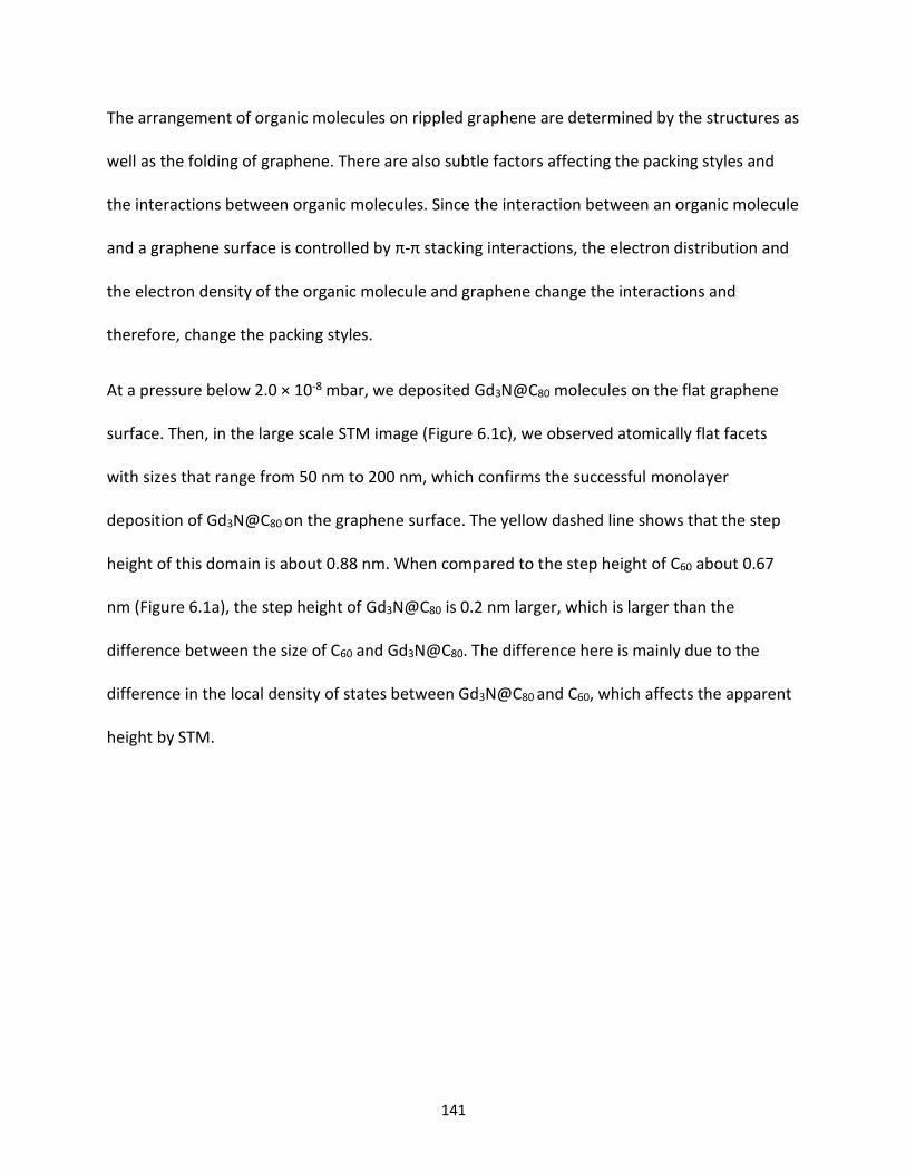
141
The arrangement of organic molecules on rippled graphene are determined by the structures as
well as the folding of graphene. There are also subtle factors affecting the packing styles and
the interactions between organic molecules. Since the interaction between an organic molecule
and a graphene surface is controlled by π-π stacking interactions, the electron distribution and
the electron density of the organic molecule and graphene change the interactions and
therefore, change the packing styles.
At a pressure below 2.0 × 10⁻⁸ mbar, we deposited Gd3N@C80 molecules on the flat graphene
surface. Then, in the large scale STM image (Figure 6.1c), we observed atomically flat facets
with sizes that range from 50 nm to 200 nm, which confirms the successful monolayer
deposition of Gd3N@C80 on the graphene surface. The yellow dashed line shows that the step
height of this domain is about 0.88 nm. When compared to the step height of C60 about 0.67
nm (Figure 6.1a), the step height of Gd3N@C80 is 0.2 nm larger, which is larger than the
difference between the size of C60 and Gd3N@C80. The difference here is mainly due to the
difference in the local density of states between Gd3N@C80 and C60, which affects the apparent
height by STM.
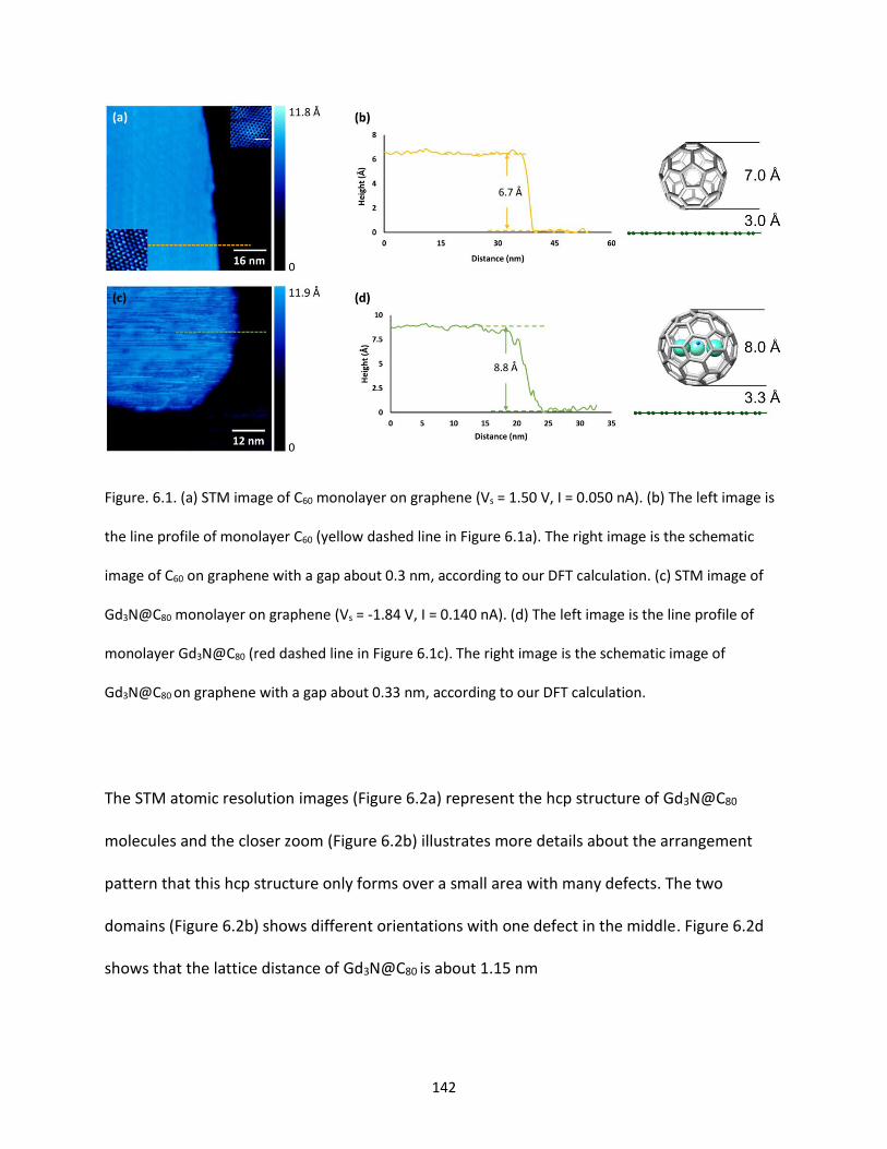
142
Figure. 6.1. (a) STM image of C60 monolayer on graphene (Vs = 1.50 V, I = 0.050 nA). (b) The left image is
the line profile of monolayer C60 (yellow dashed line in Figure 6.1a). The right image is the schematic
image of C60 on graphene with a gap about 0.3 nm, according to our DFT calculation. (c) STM image of
Gd3N@C80 monolayer on graphene (Vs = -1.84 V, I = 0.140 nA). (d) The left image is the line profile of
monolayer Gd3N@C80 (red dashed line in Figure 6.1c). The right image is the schematic image of
Gd3N@C80 on graphene with a gap about 0.33 nm, according to our DFT calculation.
The STM atomic resolution images (Figure 6.2a) represent the hcp structure of Gd3N@C80
molecules and the closer zoom (Figure 6.2b) illustrates more details about the arrangement
pattern that this hcp structure only forms over a small area with many defects. The two
domains (Figure 6.2b) shows different orientations with one defect in the middle. Figure 6.2d
shows that the lattice distance of Gd3N@C80 is about 1.15 nm
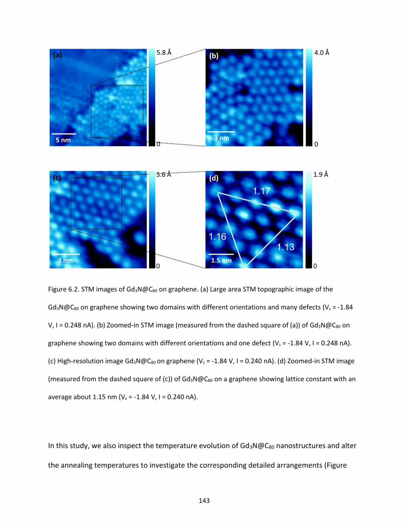
143
Figure 6.2. STM images of Gd3N@C80 on graphene. (a) Large area STM topographic image of the
Gd3N@C80 on graphene showing two domains with different orientations and many defects (Vs = -1.84
V, I = 0.248 nA). (b) Zoomed-in STM image (measured from the dashed square of (a)) of Gd3N@C80 on
graphene showing two domains with different orientations and one defect (Vs = -1.84 V, I = 0.248 nA).
(c) High-resolution image Gd3N@C80 on graphene (Vs = -1.84 V, I = 0.240 nA). (d) Zoomed-in STM image
(measured from the dashed square of (c)) of Gd3N@C80 on a graphene showing lattice constant with an
average about 1.15 nm (Vs = -1.84 V, I = 0.240 nA).
In this study, we also inspect the temperature evolution of Gd3N@C80 nanostructures and alter
the annealing temperatures to investigate the corresponding detailed arrangements (Figure
144
6.3). After annealing at 150 oC for 2 hours, Gd3N@C80 forms an hcp structure with relatively less
defects. While, with the annealing temperature increasing, Gd3N@C80 molecules tend to
aggregate together. After annealing at 200 oC for 2 hours, the Gd3N@C80 molecules still forms
the hcp structure, while some nanobubbles form on the monolayer. With higher annealing
temperature (250 oC) for 2 hours, Gd3N@C80 molecules aggregate together without forming any
ordered structure.
Figure. 6.3. (a) STM image of Gd3N@C80 on graphene after annealing at 200 oC (Vs = -1.69 V, I = 0.122
nA). (b) STM image of Gd3N@C80 on graphene after annealing at 250 oC (Vs = 1.50 V, I = 0.100 nA).
As illustrated in previous and the current studies, the highly ordered arrangements of C60 shows
relatively strong long range intermolecular interactions, while the lower ordered structure of
Gd3N@C80 indicates a relatively weak long range intermolecular interactions. It has been long
recognized that two π systems have noncovalent interactions and the π-π stacking interactions
occur in biological molecules, such as DNA, RNA and proteins, and play an essential role in
determining their 3D structures.26 It has been reported that the stacking interaction not only
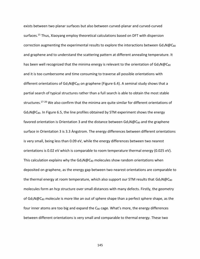
145
exists between two planar surfaces but also between curved-planar and curved-curved
surfaces.15 Thus, Xiaoyang employ theoretical calculations based on DFT with dispersion
correction augmenting the experimental results to explore the interactions between Gd3N@C80
and graphene and to understand the scattering pattern at different annealing temperature. It
has been well recognized that the minima energy is relevant to the orientation of Gd3N@C80
and it is too cumbersome and time consuming to traverse all possible orientations with
different orientations of Gd3N@C80 on graphene (Figure 6.4). A seminal study shows that a
partial search of typical structures rather than a full search is able to obtain the most stable
structures.27-28 We also confirm that the minima are quite similar for different orientations of
Gd3N@C80. In Figure 6.5, the line profiles obtained by STM experiment shows the energy
favored orientation is Orientation 3 and the distance between Gd3N@C80 and the graphene
surface in Orientation 3 is 3.3 Ȧngstrom. The energy differences between different orientations
is very small, being less than 0.09 eV, while the energy differences between two nearest
orientations is 0.02 eV which is comparable to room temperature thermal energy (0.025 eV).
This calculation explains why the Gd3N@C80 molecules show random orientations when
deposited on graphene, as the energy gap between two nearest orientations are comparable to
the thermal energy at room temperature, which also support our STM results that Gd3N@C80
molecules form an hcp structure over small distances with many defects. Firstly, the geometry
of Gd3N@C80 molecule is more like an out of sphere shape than a perfect sphere shape, as the
four inner atoms are too big and expand the C80 cage. What’s more, the energy differences
between different orientations is very small and comparable to thermal energy. These two
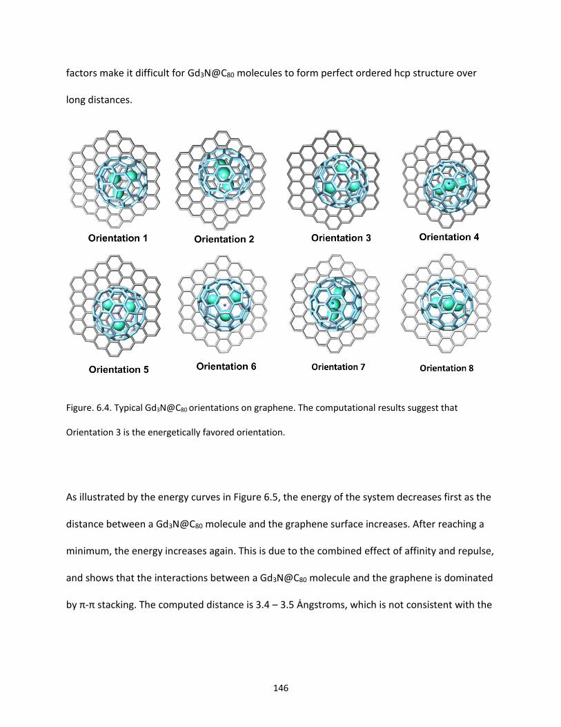
146
factors make it difficult for Gd3N@C80 molecules to form perfect ordered hcp structure over
long distances.
Figure. 6.4. Typical Gd3N@C80 orientations on graphene. The computational results suggest that
Orientation 3 is the energetically favored orientation.
As illustrated by the energy curves in Figure 6.5, the energy of the system decreases first as the
distance between a Gd3N@C80 molecule and the graphene surface increases. After reaching a
minimum, the energy increases again. This is due to the combined effect of affinity and repulse,
and shows that the interactions between a Gd3N@C80 molecule and the graphene is dominated
by π-π stacking. The computed distance is 3.4 – 3.5 Ȧngstroms, which is not consistent with the
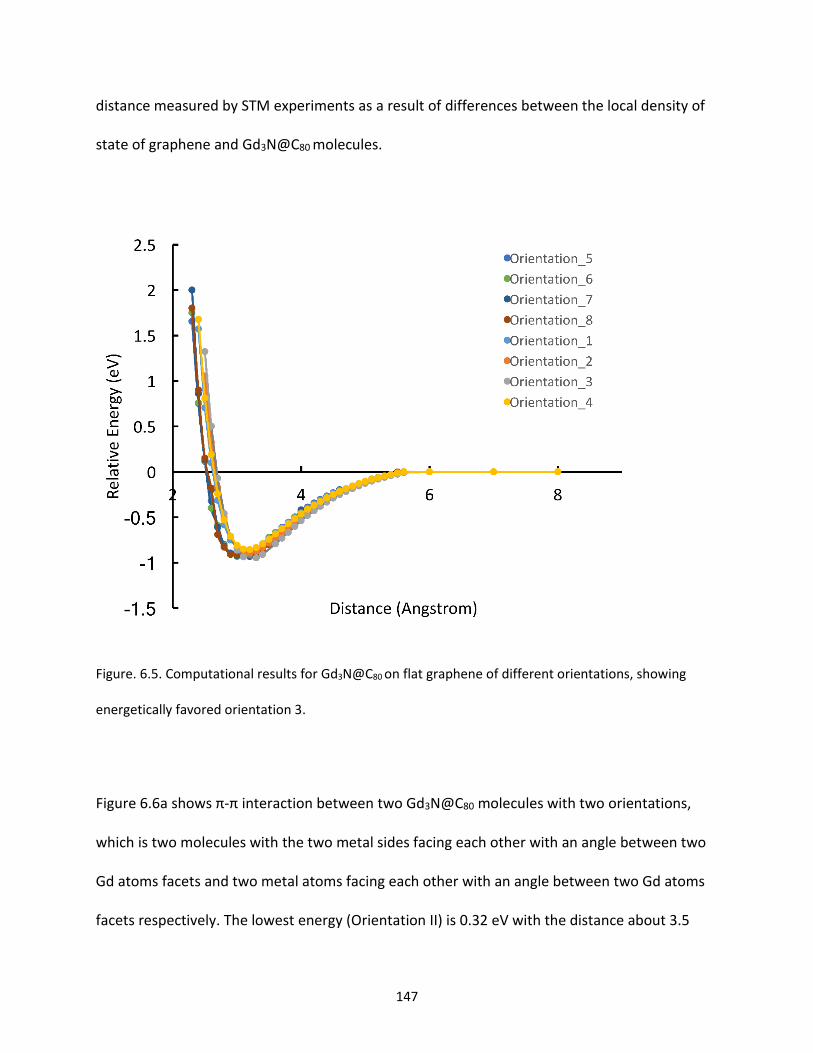
147
distance measured by STM experiments as a result of differences between the local density of
state of graphene and Gd3N@C80 molecules.
Figure. 6.5. Computational results for Gd3N@C80 on flat graphene of different orientations, showing
energetically favored orientation 3.
Figure 6.6a shows π-π interaction between two Gd3N@C80 molecules with two orientations,
which is two molecules with the two metal sides facing each other with an angle between two
Gd atoms facets and two metal atoms facing each other with an angle between two Gd atoms
facets respectively. The lowest energy (Orientation II) is 0.32 eV with the distance about 3.5
148
Ȧngstroms between molecules. The energy difference between the two orientations is only
0.02 eV, which is comparable to the thermal energy. According to our STM results, the lattice
constant of the Gd3N@C80 hcp structure is 1.15 nm, subtracting the size of the molecule of 0.8
nm, the gap between two molecules is about 0.35 nm which is highly consistent with our DFT
calculation.
Figure. 6.6. (a) DFT results for the molecule-molecule interaction of two different orientations between
two Gd3N@C80 molecules. (b) The two Gd3N@C80 molecules with two metal sides facing each other with
an angle between two Gd atoms facets. (c) The two Gd3N@C80 molecules with two metal atoms facing
each other with an angle between two Gd atoms facets.
149
6.4 Conclusion
In summary, we observed an hcp structure of Gd3N@C80 molecules on flat graphene with
characterization by both experimental STM and DFT calculations. Compared to the perfect
structure of C60 over long range, Gd3N@C80 molecules form an hcp structure over a small range
with many defects. The lattice constant that we measured is 1.15 nm and the monolayer step
height is about 0.87 nm. In addition, we studies the temperature evolution of a Gd3N@C80
monolayer on graphene. With the annealing temperature increasing, the Gd3N@C80 molecules
eventually aggregate together and break the ordered structure. Meanwhile, we compared DFT
calculations of the different orientations of a Gd3N@C80 molecule on graphene. We found the
energy favored orientation is Orientation 3 with 3.5 Ȧngstroms distance between molecule and
graphene and a binding energy of 0.95 eV. The energy difference between all orientations is
smaller than 0.09 eV. Furthermore, we calculated the binding energy between two Gd3N@C80
molecules with two orientations. The lowest energy (Orientation II) is 0.32 eV with a distance of
about 3.5 Ȧngstroms between molecules. The energy difference between two orientations is as
small as 0.02 eV. Our DFT calculation is highly agreed with our STM measurement.
References:
1. Kroto, H. W.; Heath, J. R.; Obrien, S. C.; Curl, R. F.; Smalley, R. E., C-60 - Buckminsterfullerene. Nature 1985, 318 (6042), 162-163. 2. Popov, A. A.; Yang, S. F.; Dunsch, L., Endohedral Fullerenes. Chem Rev 2013, 113 (8), 5989-6113. 3. Laasonen, K.; Andreoni, W.; Parrinello, M., Structural and Electronic-Properties of La-at-the-Cost-of-C82. Science 1992, 258 (5090), 1916-1918. 4. Zhang, J. Y.; Stevenson, S.; Dorn, H. C., Trimetallic Nitride Template Endohedral Metallofullerenes: Discovery, Structural Characterization, Reactivity, and Applications. Accounts Chem Res 2013, 46 (7), 1548-1557.
150
5. Zhang, J. Y.; Ye, Y. Q.; Chen, Y.; Pregot, C.; Li, T. H.; Balasubramaniam, S.; Hobart, D. B.; Zhang, Y. F.; Wi, S.; Davis, R. M.; Madsen, L. A.; Morris, J. R.; LaConte, S. M.; Yee, G. T.; Dorn, H. C., Gd3N@C-84(OH)(x): A New Egg-Shaped Metallofullerene Magnetic Resonance Imaging Contrast Agent. J Am Chem Soc 2014, 136 (6), 2630-2636. 6. Li, T. H.; Murphy, S.; Kiselev, B.; Bakshi, K. S.; Zhang, J. Y.; Eltahir, A.; Zhang, Y. F.; Chen, Y.; Zhu, J.; Davis, R. M.; Madsen, L. A.; Morris, J. R.; Karolyi, D. R.; LaConte, S. M.; Sheng, Z.; Dorn, H. C., A New Interleukin-13 Amino-Coated Gadolinium Metallofullerene Nanoparticle for Targeted MRI Detection of Glioblastoma Tumor Cells. J Am Chem Soc 2015, 137 (24), 7881-7888. 7. Wang, K.; Liu, X. Y.; Huang, R.; Wu, C. C.; Yang, D.; Hu, X. W.; Jiang, X. F.; Duchamp, J. C.; Dorn, H.; Priya, S., Nonionic Sc3N@C-80 Dopant for Efficient and Stable Halide Perovskite Photovoltaics. Acs Energy Lett 2019, 4 (8), 1852-1861. 8. Stevenson, S.; Rice, G.; Glass, T.; Harich, K.; Cromer, F.; Jordan, M. R.; Craft, J.; Hadju, E.; Bible, R.; Olmstead, M. M.; Maitra, K.; Fisher, A. J.; Balch, A. L.; Dorn, H. C., Small-bandgap endohedral metallofullerenes in high yield and purity (vol 401, pg 55, 1999). Nature 1999, 402 (6764), 898-898. 9. Lu, J.; Sabirianov, R. F.; Mei, W. N.; Gao, Y.; Duan, C. G.; Zeng, X. C., Structural and magnetic properties of Gd3N@C-80. J Phys Chem B 2006, 110 (47), 23637-23640. 10. Popov, A. A.; Zhang, L.; Dunsch, L., A Pseudoatom in a Cage: Trimetallofullerene Y-3@C-80 Mimics Y3N@C-80 with Nitrogen Substituted by a Pseudoatom. Acs Nano 2010, 4 (2), 795-802. 11. Nafradi, B.; Antal, A.; Pasztor, A.; Forro, L.; Kiss, L. F.; Feher, T.; Kovats, E.; Pekker, S.; Janossy, A., Molecular and Spin Dynamics in the Paramagnetic Endohedral Fullerene Gd3N@C-80. J Phys Chem Lett 2012, 3 (22), 3291-3296. 12. Tsuchiya, T.; Sato, K.; Kurihara, H.; Wakahara, T.; Maeda, Y.; Akasaka, T.; Ohkubo, K.; Fukuzumi, S.; Kato, T.; Nagase, S., Spin-site exchange system constructed from endohedral metallofullerenes and organic donors. J Am Chem Soc 2006, 128 (45), 14418-14419. 13. Cai, T.; Slebodnick, C.; Xu, L.; Harich, K.; Glass, T. E.; Chancellor, C.; Fettinger, J. C.; Olmstead, M. M.; Balch, A. L.; Gibson, H. W.; Dorn, H. C., A pirouette on a metallofullerene sphere: Interconversion of isomers of N-tritylpyrrolidino I-h Sc3N@C-80. J Am Chem Soc 2006, 128 (19), 6486-6492. 14. Chen, C. H.; Zheng, H. S.; Mills, A.; Heflin, J. R.; Tao, C. G., Temperature Evolution of Quasi-one-dimensional C-60 Nanostructures on Rippled Graphene. Sci Rep-Uk 2015, 5. 15. Li, Y. L.; Liu, X. Y.; Chen, C. H.; Duchamp, J.; Huang, R.; Chung, T. F.; Young, M.; Chalal, T.; Chen, Y. P.; Heflin, J. R.; Dorn, H. C.; Tao, C. G., Differences in self-assembly of spherical C-60 and planar PTCDA on rippled graphene surfaces. Carbon 2019, 145, 549-555. 16. Shinohara, H.; Hayashi, N.; Sato, H.; Saito, Y.; Wang, X. D.; Hashizume, T.; Sakurai, T., Direct Stm Imaging of Spherical Endohedral Sc-2-at-C-84 Fullerenes. J Phys Chem-Us 1993, 97 (51), 13438-13440. 17. Reveles, J. U.; Karle, N. N.; Baruah, T.; Zope, R. R., Electronic and Structural Properties of C-60 and Sc3N@C-80 Supported on Graphene Nanoflakes. J Phys Chem C 2016, 120 (45), 26083-26092. 18. Tian, X. Q.; Xu, J. B.; Wang, X. M., Self-Assembly of PTCDA Ultrathin Films on Graphene: Structural Phase Transition and Charge Transfer Saturation. J Phys Chem C 2010, 114 (49), 20917-20924. 19. Li, G.; Zhou, H. T.; Pan, L. D.; Zhang, Y.; Mao, J. H.; Zou, Q.; Guo, H. M.; Wang, Y. L.; Du, S. X.; Gao, H. J., Self-assembly of C-60 monolayer on epitaxially grown, nanostructured graphene on Ru(0001) surface. Appl Phys Lett 2012, 100 (1). 20. Ren, J.; Meng, S.; Wang, Y. L.; Ma, X. C.; Xue, Q. K.; Kaxiras, E., Properties of copper (fluoro-)phthalocyanine layers deposited on epitaxial graphene. J Chem Phys 2011, 134 (19). 21. Wang, Q. H.; Hersam, M. C., Room-temperature molecular-resolution characterization of self-assembled organic monolayers on epitaxial graphene. Nat Chem 2009, 1 (3), 206-211. 22. Lu, J.; Yeo, P. S. E.; Zheng, Y.; Yang, Z. Y.; Bao, Q. L.; Gan, C. K.; Loh, K. P., Using the Graphene Moire Pattern for the Trapping of C-60 and Homoepitaxy of Graphene. Acs Nano 2012, 6 (1), 944-950.
151
23. Cho, J.; Smerdon, J.; Gao, L.; Suzer, O.; Guest, J. R.; Guisinger, N. P., Structural and Electronic Decoupling of C-60 from Epitaxial Graphene on SiC. Nano Lett 2012, 12 (6), 3018-3024. 24. Chen, L.; Carpenter, E. E.; Hellberg, C. S.; Dorn, H. C.; Shultz, M.; Wernsdorfer, W.; Chiorescu, I., Spin transition in Gd3N@C-80, detected by low-temperature on-chip SQUID technique. J Appl Phys 2011, 109 (7). 25. Sinha, S.; Sheng, Y. W.; Griffiths, I.; Young, N. P.; Zhou, S.; Kirkland, A. I.; Porfyrakis, K.; Warner, J. H., In Situ Atomic-Level Studies of Gd Atom Release and Migration on Graphene from a Metallofullerene Precursor. Acs Nano 2018, 12 (10), 10439-10451. 26. Hunter, C. A.; Sanders, J. K. M., The Nature of Pi-Pi Interactions. J Am Chem Soc 1990, 112 (14), 5525-5534. 27. Cabaleiro-Lago, E. M.; Rodriguez-Otero, J.; Carrazana-Garcia, J. A., A theoretical study of complexes between fullerenes and concave receptors with interest in photovoltaics. Phys Chem Chem Phys 2017, 19 (39), 26787-26798. 28. Gonzalez-Veloso, I.; Rodriguez-Otero, J.; Cabaleiro-Lago, E. M., Carbon-nanorings ([10]CPP and [6]CPPA) as fullerene (C-60 and C-70) receptors: a comprehensive dispersion-corrected DFT study. Phys Chem Chem Phys 2016, 18 (46), 31670-31679.
152
Chapter 7
Conclusion and Future Work
The experiments discussed in this dissertation have focused on the molecular self-assembly
behavior of PCBM, PTCDA, C60 and Gd3N@C80 molecules on planar graphene and rippled
graphene by experimental STM and AFM methods and theoretical DFT calculations. The main
motivation in this dissertation is to investigate the mechanism behind molecular self-assembly
behavior to aid in the development of the future graphene applications. Here, we present a
summary of the conclusions and the potential future work for this area of research.
7.1 The Bilayer PCBM Structure Formed on Graphene and HOPG
In the first part of our investigation, we demonstrated the self-assembly behavior of PCBM
bilayer nanostructures on HOPG and graphene, by using STM and AFM, and analyzed the
observed structure by comparison to molecular models. Through careful control of the PCBM
solution concentration (from 0.1 mg/ml to 2 mg/ml) and the deposition conditions, we
demonstrate that PCBM molecules self-assemble into bilayer structures with increasing
coverage on graphene and HOPG substrates. Interestingly, the PCBM bilayer revealed two
distinct configurations on HOPG with two different heights (1.64 nm and 1.23 nm respectively),
and only one configuration (1.37 nm) on graphene. We also found two monolayer
configurations on HOPG with two different heights (0.71 nm and 0.88 nm respectively) and one
153
configuration of 0.87 nm on graphene. We believe the two configurations of a bilayer are due
to the different tiled angle by contracting the model of molecular dimer. While, for the
monolayer, the two configurations are more due to the standing up or laying down position of
PCBM molecules. Post thermal annealing could induce the merging of bilayer nanostructures
due to the edge diffusion. This is, to the best of our knowledge, the first experimental
realization of PCBM bilayer structures on graphene. Our results will shed light on improvement
of the energy efficiency in solar cells containing graphene and organic molecules, by increasing
the donor-acceptor interface area.
7.2 The Ordered of C60 and Disordered Structure of PTCDA Formed on Rippled Graphene
In the second part, we have found the self-assembly of PTCDA and C60 molecules on rippled
graphene with by using both STM and DFT calculations. The adsorbed molecules on 1D-rippled
graphene systems show distortions when compared with analogous planar graphene system.
Specifically, the nearly spherical C60 molecules form a quasi-hexagonal close packed structure,
while the planar PTCDA molecules form a disordered herringbone structure on the rippled
graphene surface. The change in the packing pattern of C60 and PTCDA molecules on a curved
graphene surface is due to competition between the intermolecular adsorbate interactions and
the adsorbate-graphene interaction. Because of the nearly spherical C60 molecules, the rippled
graphene surface exhibits only depreciated effects on the π-π intermolecular interactions. In
opposition, the planar PTCDA molecules receive the effect that is more significant by the
rippled graphene. In addition, the DFT computational results demonstrate significant increases
154
in π-π interactions for both the adsorbed PTCDA and C60/rippled graphene complexes located
in the 2D graphene valley sites compared with adsorbed more idealized molecule/planar
graphene 2D complexes. Furthermore, we find that the adsorbed planar PTCDA molecules
prefer different orientations when on the rippled graphene peak regions compared to the
valley regions. These fundamental experimental and computational results are important for
understanding any potential application of structurally diverse molecules adsorbed on
graphene and/or rippled graphene surfaces.
7.3 The hcp Structure of Gd3N@C80 Formed on Graphene
In last part, we reported hcp structure of Gd3N@C80 molecules on flat graphene with
characterization using both experimental STM and DFT calculations. Comparable to the perfect
structure of C60 in long range, Gd3N@C80 molecules forms hcp structure in small range with
many defects. The lattice constant that we measured is 1.15 nm and the monolayer step height
is about 0.87 nm. Besides, we did the temperature evolution of Gd3N@C80 monolayer on
graphene. With the annealing temperature increasing, the Gd3N@C80 molecules would
aggregate together breaking the ordered structure. Meanwhile, we did the DFT calculation
about the different orientations of Gd3N@C80 molecule on graphene. We found the energy
favorite orientation is orientation 6 with 3.5 angstroms distance between molecule and
graphene and binding energy of 0.95 eV. The energy difference between all orientations is
smaller than 0.09 eV, while the energy differences between two nearest orientations is 0.02 eV
which is compared to room temperature thermal energy (0.025 eV). That means the
155
orientation of Gd3N@C80 molecule could change easily in room temperature. What’s more, we
calculated the binding energy between two Gd3N@C80 molecules with two orientations. The
lowest energy (orientation 2) is 0.32 eV with the distance about 3.5 angstroms between
molecules. The energy difference between two orientations is as small as 0.2 eV. Our DFT
calculation is highly agreed with our STM measurement. This is, to the best of our knowledge,
the first experimental realization of Gd3N@C80 molecules monolayer structures on graphene.
These fundamental experimental and computational results are important for understanding
any potential application of Gd3N@C80 molecules adsorbed on graphene.
7.4 Future Work
The immediate next step in this project is the investigation of molecular self-assembly behavior
of the mixture of organic semiconductor donor and acceptor molecules (such as C60 and
DTS(PTTh2)2 and other combinations) on graphene substrate. This is of interest as donor
acceptor combinations are essential for efficient organic photovoltaics (OPVs). We are hoping
to see the phase separation of donor and acceptor molecules on graphene substrate. OPVs
require proximity of the donors and acceptors for charge transfer and bicontinuous networks to
enable charge transfer to the substrate. Besides, we could better understand the interaction
and mechanism between donor and acceptor molecules by combining scanning tunneling
microscope (STM) and scanning tunneling spectroscopy (STS) to study the molecules at both
sides of the interfere between donor and acceptor domains, especially at low temperature. This
156
could help us better understand the mechanism behind organic solar cell for the goal of
increasing the efficiency.
In addition, it would be useable to examine other members of the fullerene familiy including
metallofullerenes. For example, we could study magnetic phenomena and charge transfer
effect of Gd3N@C80 molecule by using a magnetic tip. We could also study the electronic
properties and morphology of larger fullerenes, like C90, C100 and C120. C120 is the largest
fullerene molecule and was an interesting structure. A C120 molecule is an armchair carbon
nanotube with two C60 hemisphere at the two ends. The electronic properties of C120 are very
interesting as the armchair carbon nanotube is metallic while the C60 is semiconductor.
The most important future direction of the project is the molecular self-assembly on graphene
established by other forces. For now, the molecular self-assembly behavior on graphene is all
based on hydrogen bonding. For example, we could study the molecular self-assembly behavior
on graphene induced by molecules and metal atoms. Besides, the halogen-halogen molecule
self-assembly behavior on graphene is also a good topic for investigation by depositing
hexakis(4-iodophenyl)benzene (HPBI) molecules on graphene.
157
List of Publications
The work of this thesis is partial based on the following publications:
1. Li, Y.; Chen, C.; Burton, J.; Park, K.; Heflin, J.; Tao, C., Self-Assembled PCBM Bilayers on
Graphene and HOPG Examined by AFM and STM, Nanotechnology 29, 185703 (2018)
2. Li, Y.; Liu, X.; Chen, C.; Duchamp, J.; Huang, R.; Chung, T.; Young, M.; Chalal, T.; Chen, Y.P.;
Heflin, J.R.; Dorn, H.; Tao, C., Differences in Self-Assembly of Spherical C60 and Planar PTCDA on
Rippled Graphene Surfaces, Carbon 145, 549 (2019)