1
Innovation with Integrity Atomic Force Microscopy Scanning Probe Microscopy ©2011 Copyright Bruker Corporation. All rights reserved. MultiMode 8, VITA, TappingMode, LiftMode, PhaseImaging, PeakForce Tapping, PeakForce QNM, ScanAsyst, NanoProbes, TESP and FESP are trademarks of Bruker Corporation. SPM Operation Scanning Probe Microscopy (SPM) is a technique to provide spatially localized three-dimensional information by raster scanning a sharp probe across a surface of interest while monitoring the cantilever deflection from the probe sample interaction. Depending on the interaction, in addition to topographic information, a variety of surface properties can be measured (such as electrical, magnetic, and mechanical). The main SPM scan modes are contact mode, TappingMode , and PeakForce Tapping , and these build the foundation of all Z X Y X Y Feedback Loop Output Signal Adjusts Z Position Raster Scan Probe Sample Detector Signal PeakForce Tapping TappingMode PeakForce Tapping (PFT) is a Bruker-exclusive AFM mode optimized to achieve simultaneous high-resolution images and quantitative mechanical measurements. During operation, the cantilever is brought in and out of contact with the surface in a non-resonant cycle, where the PFT algorithms directly control the instantaneous force interaction. Because the entire cycle is monitored and recorded, PFT provides force spectroscopy information at each pixel. In the feedback mode, the instantaneous peak force is limited; TappingMode is a primary SPM mode. During operation, a “tapping piezo” mechanically oscillates the probe at or near its fundamental resonance frequency. The oscillating probe is brought into intermittent contact with the sample to be imaged until the "tapping" between the tip and the sample reduces the cantilever oscillation to a predetermined level. The controller records the cantilever's oscillation amplitude and its phase relative to the drive signal. A feedback loop is employed to adjust the Z position of the sample to maintain a constant tapping amplitude. TappingMode enables numerous secondary modes, including PhaseImaging , EFM, MFM, and KPFM. Preferred Bruker probes for this application include SNL-10, DNP-10, MLCT, and MSNL-10. Contact Mode LiftMode Magnetic Force Microscopy (MFM) uses a combination of TappingMode , LiftMode and a properly prepared tip to gather information about the magnetic field above a sample. Each line of the sample is first scanned in TappingMode to obtain the sample topography. The topographic information is stored and retraced with a user-selectable height offset in LiftMode. During the lift-trace, the magnetic data is collected by measuring the variations in the phase signal. Typical lift heights in MFM range from 20-100 nm. Preferred Bruker probes for this application include MESP, MESP-HM, MESP-LM, and MESP-RC. Contact Mode is the original SPM mode, and while not as popular as intermittent contact modes for imaging, it remains in regular use. In contact mode, the tip and sample are in direct contact throughout the raster-scan. The detector measures the deflection of the cantilever in response to the sample topography. During imaging, the sample is either held at a fixed height (Constant Height Mode) or modulated via a feedback loop to adjust the position of the sample to hold the cantilever deflection constant (Constant Force Mode). Contact Mode enables numerous secondary modes, such as LFM, SCM, SSRM, TUNA, and CAFM. Preferred Bruker probes for this application include ESP, MPP-31100-10, SNL-10, DNP-10, MLCT, and MSNL-10. A Time E B C D approach withdraw A B C E D Z X Y X Y Detector Signal Drive Signal Feedback Loop Output Signal Adjusts Z Position Feedback Loop Maintains Constant Cantilever Amplitude Raster Scan potentially down to the pN level. In the PeakForce QNM Imaging Mode, the spectroscopic information is analyzed in real time to report modulus, adhesion, energy dissipation and deformation, along with topography. The ScanAsyst Imaging Mode is a PFT variant that automatically optimizes all imaging parameters. Preferred Bruker probes for this application include ScanAsyst-Air, ScanAsyst-Fluid, and ScanAsyst-Fluid+. advanced scanning techniques. Preferred Bruker probes for this application include TESP, RTESP, ESP, SNL-10, DNP-10, MLCT, and MSNL-10. Polymer brush sample imaged on a MultiMode ® 8 using ScanAsyst. Sample courtesy of S. Sheiko, University of North Carolina, Chapel Hill. Protein molecules in liquid before and after force pulling with AFM. Topography of antimony dendrites on graphite. Raster Scan Z X Y X Y Feedback Loop Maintains Constant Cantilever Deflection Feedback Loop Output Signal Adjusts Z Position Magnetic domains in a steel sample. EFM sample. Lift Height LiftMode Scan TappingMode Height Data LiftMode Scan Height Data = Phase Shift Lift Height Magnetic Probe Magnetic Forces Cause Phase Shift over Different Domains during the LiftMode Scan LiftMode is not an imaging mode, but rather a technique that enables other modes such as MFM, EFM, and SCM. In LiftMode, the topography of the sample is first recorded in a regular topographic mode such as Contact Mode, TappingMode or PeakForce Tapping . The following line, the “lift line,” re-traces the previously acquired topography with an added Z-offset, allowing the desired contrast mechanism to be separated from the topography. Since the sample topography has already been recorded, the feedback laser is not strictly necessary during the lift line, and it can be turned off where experiments would be influenced by laser light. This variation is called “DarkLift Mode” and is most commonly used in electrical applications on semiconductors. Preferred Bruker probes for this application include MESP, SCM-PIT, and SCM-PIC. Magnetic Force For more information visit www.bruker-axs.com or www.brukerafmprobes.com Electrostatic Force Surface Potential Scanning Tunneling TUNA & Conductive Scanning Spreading Resistance Scanning Capacitance Piezoresponse Scanning Thermal Critical Dimension Conductive AFM Probe Contact Mode Si n p V DC (Sub pA - 100 μA) TUNA Data Current Amplifier Topography Native Collagen fibrils exhibiting the typical 67nm banding pattern. STM is the original embodiment of the SPM and it remains one of the primary modes. In STM, the probe is not a cantilever, but a metal needle, held perpendicular to the sample. The contrast mechanism is the tunneling current between the tip and sample when an electrical bias is applied. In feedback mode, the tip-sample tunneling gap is adjusted in order to maintain a predetermined constant current. Preferred Bruker probes for this application include TT10, PT10, STM, CLST-PTBO, DPT10, DTT10, PT-ECM10, and TT-ECM10. In-situ atom resolution electrochemical STM image of Cu underpotential deposition on Au(111). Composite image of Height and Surface potential of a laser diode (8 μm scan). Carbon black aggregates in a rubber matrix visualized by utilizing their electric properties. Surface Potential Imaging (often called Kelvin Probe Force Microscopy or KPFM) uses a conductive probe to image work function differences between the tip and the sample. KPFM is accomplished in LiftMode by applying an AC and DC bias to the probe. The AC bias is applied at the probe's fundamental resonance frequency. The DC bias is adjusted through a feedback loop such that no mechanical oscillation is induced from the AC bias. This null condition occurs when the DC bias exactly offsets the work function difference. Using LiftMode achieves the highest sensitivity for the smallest potential differences by eliminating any mechanical disturbance and utilizing resonant enhancement. Alternatively, surface potential can be obtained in a single-pass, using dual frequency, to eliminate topographic artifacts that can be caused by electrostatic forces when the potential differences are large. Preferred Bruker probes for this application include SCM-PIT, MESP, MESP-RC, and OSCM-PT. Scanning Spreading Resistance (SSRM) operates in the contact mode using a conductive probe. The imaging signal is the electric current between the tip and sample for an applied DC bias. SSRM is similar to CAFM in that it measures the current by referencing it to an internal resistor. However, unlike CAFM, SSRM uses a logarithmic amplifier to extend the range of measurable local resistance value (at the expense of frequency response). The preferred Bruker probe for this application is DDESP. Topography (left), SCM (right) laser diode cross section. Conductive Polymer (right), Poly-analine on Indium Tin Oxide (left). Critical Dimension Atomic Force Microscopy (CDAFM) is a nondestructive, high-resolution SPM technique that enables accurate measurement of three-dimensional (3D) features. CDAFM is accurate as it provides highly linear measurement over a range of line-widths and is unaffected by feature type, density or material type. Additionally, the technique is able to measure undercut features and can be calibrated using NIST-traceable calibration standards to ensure accuracy of measurements. CDAFM capabilities have enabled its use as a reference metrology tool. Preferred Bruker probes are the 3D Metrology Probes. Piezoresponse (Piezoforce) Microscopy (PFM) is a technique based on contact mode that maps out the inverse piezoelectric effect on a sample. The sample is electrically stimulated and the topographic response of the sample is monitored using lock-in techniques. Amplitude and phase channels reveal information about the strength and direction of the polarization on the sample. Preferred Bruker probes for this application include MESP-RC, SCM-PIT, MESP, and DDESP-FM. Topography and thermal map of a data storage sample. In Scanning Thermal Microscopy (SThM) a heated tip is scanned across a sample. Changes in the tip’s resistivity reveal either thermal conductivity or thermal gradients on the sample. In Nanoscale Analysis (NA) a tip is heated in such a way that it induces a phase transition in the sample. That transition is monitored using the cantilever deflection and is material specific. Preferred Bruker probes for this application include 1610-00, VITA NanoTA Probes, and VITA SThM Probes. LiftMode Scan Height Data = Phase Shift Lift Height Conductive Probe Electric Forces Cause Phase Shift over Different Domains during the LiftMode Scan Single Pass (Dual Frequency) is also available Electrostatic Force Microscopy (EFM) uses a combination of TappingMode , LiftMode and a conductive tip to gather information about the electric field above a sample. Each line of the sample is first scanned in TappingMode to obtain the sample topography. The topographic information is stored and retraced with a user-selectable height offset in LiftMode. During the lift-trace, the electrostatic force data is collected by measuring the variations in the phase signal. Alternatively, phase shift can be used as a feedback signal moving the imaging contrast to frequency shift; making this mode useful for quantitative interpretations. Typical lift heights in EFM range from 20-80 nm. Preferred Bruker probes for this application include SCM-PIT, MESP, MESP-RC, and OSCM-PT. LiftMode Scan Height Data Lift Height 2V Potential Data 0V -1V Conductive Probe Single Pass (Dual Frequency) Capacity is also available Z X Y X Y DC Bias Tunneling Current Amplifier Feedback Loop Maintains Constant Tunneling Current Feedback Loop Output Signal Adjusts Z Position XY Raster Scan Tunneling AFM (TUNA) and Conductive AFM traditionally operate in contact mode using a conductive probe. The imaging signal is the electric current between tip and sample for an applied DC bias. In the feedback mode, rather than letting the current vary over the sample, the DC bias is dynamically adjusted to maintain a constant tip-sample current. The operational current ranges is from fA (TUNA) to μA (CAFM). More recently, CAFM and TUNA have been utilized with PeakForce Tapping , enabling these measurements to be taken more reliably and on a much wider range of samples, as well as allowing for the direct correlation of electrical data with nanomechanical information from PeakForce QNM measurements. Applications range from studies of dielectric strength and thickness uniformity in thin films to electronic properties of semiconductor, nano-structures, and conductive polymers. Preferred Bruker probes for this application include SCM-PIC, SCM-PIT, and DDESP-FM. Conductive AFM Probe Contact Mode (SSRM Data) (10 pA - 100 μA) Logarithmic Amplifier log (I) Si n p Spreading Resistance R = 4 x radius V DC ρ Resistance Conductive AFM Probe Contact Mode Si n p V AC SCM Data Capacitance Sensor SCM Sensor Topography n n n p p Scanning Capacitance Microscopy (SCM) can be used on flat, well-prepared semiconductor surfaces to map the relative changes of majority carrier concentrations. SCM operates in contact mode by forming a metal-insulator-semiconductor capacitor between the tip and the sample. This capacitor is measured using an ultrahigh-frequency (1 GHz) detector as it is varied with an applied AC + DC bias. The AC (~90 kHz) + DC bias is set to create capacitance variations through the accumulation and depletion of the surface layers. SCM does not directly measure capicatance, but DC/DV. In the Bruker-exclusive feedback mode, DV is adjusted to maintain a constant DC/DV to keep the depletion volume constant, which improves the mapping accuracy of dopant boundaries. To further enhance this accuracy, SCM can be combined with Dark Lift, avoiding photoelectric artifacts. Preferred Bruker probes for this application include SCM-PIC, SCM-PIT, MESP-RC, and OSCM-PT. Multiple semiconductor trenches. Small defect on the poling boundary of a Lithium niobate film visible in the amplitude signal of a PFM experiment. Temperature Measurement Vertical Deflection Monitored as Tip Heated Heater Control T Δ Thermal Property Map Topographical Map Topographical Measurement Flare of Tip Enables Measurements of Undercut Features Bottom CD Sidewall Profile Sidewall Angles Middle CD Top CD Depth Line Width Roughness LWR & LER Transistor cross section.

Scanning Probe Microscopy Modes - The Molecular …mmrc.caltech.edu/AFM Dimension Icon/Bruker Training/SPM_Modes.pdf · SPM Operation Scanning Probe Microscopy (SPM) is a technique

Embed Size (px)

Citation preview

Innovation with IntegrityAtomic Force Microscopy

Scanning Probe Microscopy

©2011 Copyright Bruker Corporation. All rights reserved. MultiMode 8, VITA, TappingMode, LiftMode, PhaseImaging, PeakForce Tapping, PeakForce QNM, ScanAsyst, NanoProbes, TESP and FESP are trademarks of Bruker Corporation.

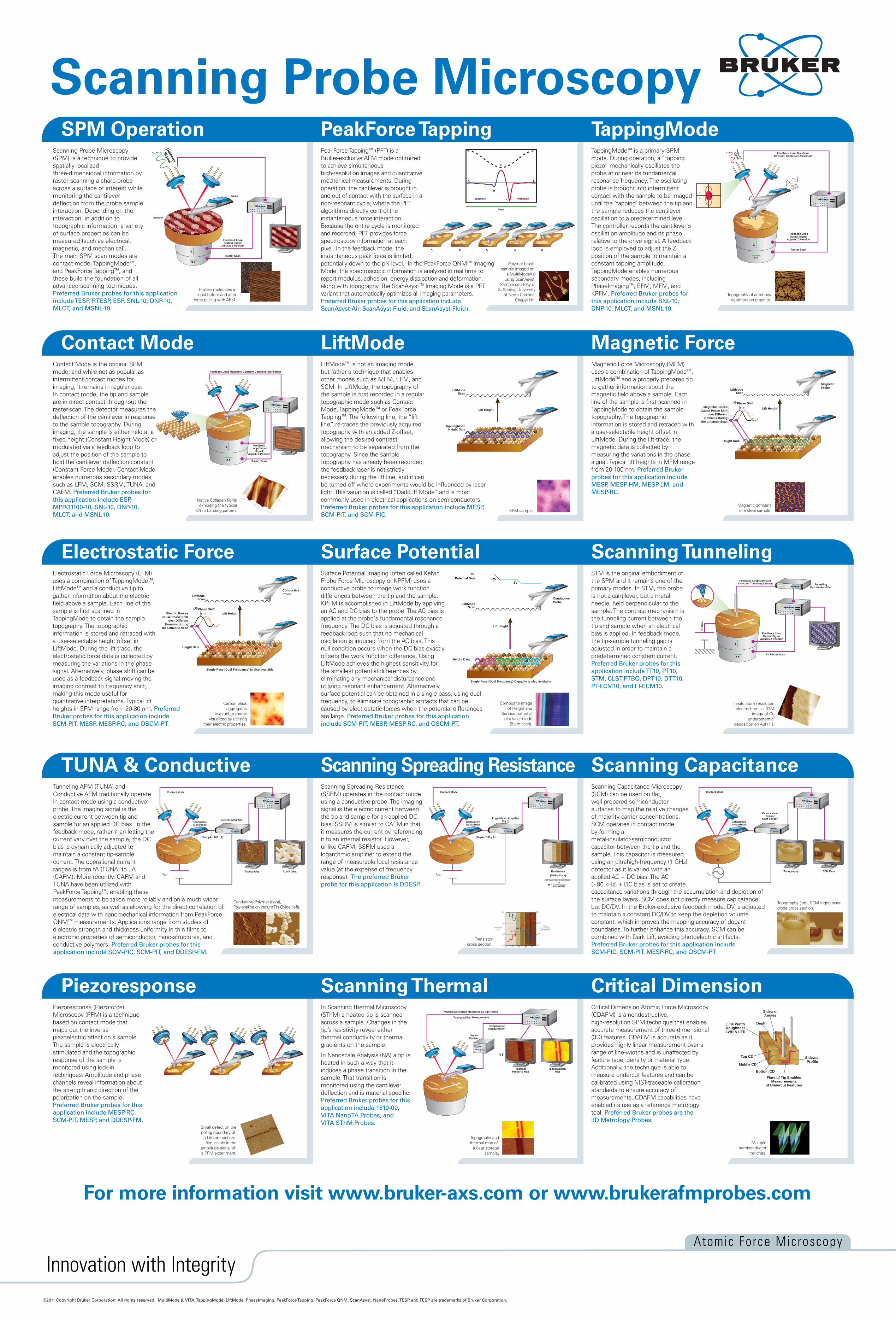
SPM OperationScanning Probe Microscopy (SPM) is a technique to provide spatially localized three-dimensional information by raster scanning a sharp probe across a surface of interest while monitoring the cantilever deflection from the probe sample interaction. Depending on the interaction, in addition to topographic information, a variety of surface properties can be measured (such as electrical, magnetic, and mechanical). The main SPM scan modes are contact mode, TappingMode™, and PeakForce Tapping™, and these build the foundation of all

ZZ

X YX Y

Feedback LoopOutput Signal

Adjusts Z Position

Raster Scan

Probe

Sample

Detector

Signal

PeakForce Tapping TappingModePeakForce Tapping™ (PFT) is a Bruker-exclusive AFM mode optimized to achieve simultaneous high-resolution images and quantitative mechanical measurements. During operation, the cantilever is brought in and out of contact with the surface in a non-resonant cycle, where the PFT algorithms directly control the instantaneous force interaction. Because the entire cycle is monitored and recorded, PFT provides force spectroscopy information at each pixel. In the feedback mode, the instantaneous peak force is limited;

TappingMode™ is a primary SPM mode. During operation, a “tapping piezo” mechanically oscillates the probe at or near its fundamental resonance frequency. The oscillating probe is brought into intermittent contact with the sample to be imaged until the "tapping" between the tip and the sample reduces the cantilever oscillation to a predetermined level. The controller records the cantilever's oscillation amplitude and its phase relative to the drive signal. A feedback loop is employed to adjust the Z position of the sample to maintain a constant tapping amplitude. TappingMode enables numerous secondary modes, including PhaseImaging™, EFM, MFM, and KPFM. Preferred Bruker probes for this application include SNL-10, DNP-10, MLCT, and MSNL-10.

Contact Mode LiftModeMagnetic Force Microscopy (MFM) uses a combination of TappingMode™, LiftMode™ and a properly prepared tip to gather information about the magnetic field above a sample. Each line of the sample is first scanned in TappingMode to obtain the sample topography. The topographic information is stored and retraced with a user-selectable height offset in LiftMode. During the lift-trace, the magnetic data is collected by measuring the variations in the phase signal. Typical lift heights in MFM range from 20-100 nm. Preferred Bruker probes for this application include MESP, MESP-HM, MESP-LM, and MESP-RC.

Contact Mode is the original SPM mode, and while not as popular as intermittent contact modes for imaging, it remains in regular use. In contact mode, the tip and sample are in direct contact throughout the raster-scan. The detector measures the deflection of the cantilever in response to the sample topography. During imaging, the sample is either held at a fixed height (Constant Height Mode) or modulated via a feedback loop to adjust the position of the sample to hold the cantilever deflection constant (Constant Force Mode). Contact Mode enables numerous secondary modes, such as LFM, SCM, SSRM, TUNA, and CAFM. Preferred Bruker probes for this application include ESP, MPP-31100-10, SNL-10, DNP-10, MLCT, and MSNL-10.

A

Time

E

B

C

Dapproach withdraw

A B C ED

Z

X YX Y

Detector

Signal

Drive

Signal

Feedback LoopOutput Signal

Adjusts Z Position

Feedback Loop MaintainsConstant Cantilever Amplitude

Raster Scan

potentially down to the pN level. In the PeakForce QNM™ Imaging Mode, the spectroscopic information is analyzed in real time to report modulus, adhesion, energy dissipation and deformation, along with topography. The ScanAsyst™ Imaging Mode is a PFT variant that automatically optimizes all imaging parameters. Preferred Bruker probes for this application include ScanAsyst-Air, ScanAsyst-Fluid, and ScanAsyst-Fluid+.

advanced scanning techniques.Preferred Bruker probes for this application include TESP, RTESP, ESP, SNL-10, DNP-10, MLCT, and MSNL-10.

Polymer brush sample imaged on

a MultiMode® 8using ScanAsyst.

Sample courtesy ofS. Sheiko, University

of North Carolina,Chapel Hill.

Protein molecules in liquid before and after

force pulling with AFM.Topography of antimony

dendrites on graphite.

Raster Scan

Z

X YX Y

Feedback Loop Maintains Constant Cantilever Deflection

FeedbackLoop Output

SignalAdjusts Z Position

Magnetic domainsin a steel sample.EFM sample.

Lift Height

LiftModeScan

TappingModeHeight Data

LiftModeScan

Height Data

= Phase ShiftLift Height

MagneticProbe

Magnetic ForcesCause Phase Shift

over DifferentDomains during

the LiftMode Scan

LiftMode™ is not an imaging mode, but rather a technique that enables other modes such as MFM, EFM, and SCM. In LiftMode, the topography of the sample is first recorded in a regular topographic mode such as Contact Mode, TappingMode™ or PeakForce Tapping™. The following line, the “lift line,” re-traces the previously acquired topography with an added Z-offset, allowing the desired contrast mechanism to be separated from the topography. Since the sample topography has already been recorded, the feedback laser is not strictly necessary during the lift line, and it can be turned off where experiments would be influenced by laser light. This variation is called “DarkLift Mode” and is most commonly used in electrical applications on semiconductors. Preferred Bruker probes for this application include MESP, SCM-PIT, and SCM-PIC.

Magnetic Force

For more information visit www.bruker-axs.com or www.brukerafmprobes.com

Electrostatic Force Surface Potential Scanning Tunneling

TUNA & Conductive Scanning Spreading Resistance Scanning Capacitance

Piezoresponse Scanning Thermal Critical Dimension

ConductiveAFM Probe

Contact Mode

Si

n p

VDC

(Sub pA - 100 μA)

TUNA Data

Current Amplifier

Topography

Native Collagen fibrils exhibiting the typical

67nm banding pattern.

STM is the original embodiment of the SPM and it remains one of the primary modes. In STM, the probe is not a cantilever, but a metal needle, held perpendicular to the sample. The contrast mechanism is the tunneling current between the tip and sample when an electrical bias is applied. In feedback mode, the tip-sample tunneling gap is adjusted in order to maintain a predetermined constant current. Preferred Bruker probes for this application include TT10, PT10, STM, CLST-PTBO, DPT10, DTT10, PT-ECM10, and TT-ECM10.

In-situ atom resolutionelectrochemical STM

image of Cuunderpotential

deposition on Au(111).

Composite imageof Height and

Surface potentialof a laser diode

(8 μm scan).

Carbon black aggregates

in a rubber matrixvisualized by utilizing

their electric properties.

Surface Potential Imaging (often called Kelvin Probe Force Microscopy or KPFM) uses a conductive probe to image work function differences between the tip and the sample. KPFM is accomplished in LiftMode by applying an AC and DC bias to the probe. The AC bias is applied at the probe's fundamental resonance frequency. The DC bias is adjusted through a feedback loop such that no mechanical oscillation is induced from the AC bias. This null condition occurs when the DC bias exactly offsets the work function difference. Using LiftMode achieves the highest sensitivity for the smallest potential differences by eliminating any mechanical disturbance and utilizing resonant enhancement. Alternatively, surface potential can be obtained in a single-pass, using dual frequency, to eliminate topographic artifacts that can be caused by electrostatic forces when the potential differences are large. Preferred Bruker probes for this application include SCM-PIT, MESP, MESP-RC, and OSCM-PT.

Scanning Spreading Resistance (SSRM) operates in the contact mode using a conductive probe. The imaging signal is the electric current between the tip and sample for an applied DC bias. SSRM is similar to CAFM in that it measures the current by referencing it to an internal resistor. However, unlike CAFM, SSRM uses a logarithmic amplifier to extend the range of measurable local resistance value (at the expense of frequency response). The preferred Bruker probe for this application is DDESP.

Topography (left), SCM (right) laserdiode cross section.

Conductive Polymer (right), Poly-analine on Indium Tin Oxide (left).

Critical Dimension Atomic Force Microscopy (CDAFM) is a nondestructive, high-resolution SPM technique that enables accurate measurement of three-dimensional (3D) features. CDAFM is accurate as it provides highly linear measurement over a range of line-widths and is unaffected by feature type, density or material type. Additionally, the technique is able to measure undercut features and can be calibrated using NIST-traceable calibration standards to ensure accuracy of measurements. CDAFM capabilities have enabled its use as a reference metrology tool. Preferred Bruker probes are the 3D Metrology Probes.

Piezoresponse (Piezoforce) Microscopy (PFM) is a technique based on contact mode that maps out the inverse piezoelectric effect on a sample. The sample is electrically stimulated and the topographic response of the sample is monitored using lock-in techniques. Amplitude and phase channels reveal information about the strength and direction of the polarization on the sample. Preferred Bruker probes for this application include MESP-RC, SCM-PIT, MESP, and DDESP-FM.

Topography andthermal map of

a data storagesample.

In Scanning Thermal Microscopy (SThM) a heated tip is scanned across a sample. Changes in the tip’s resistivity reveal either thermal conductivity or thermal gradients on the sample.

In Nanoscale Analysis (NA) a tip is heated in such a way that it induces a phase transition in the sample. That transition is monitored using the cantilever deflection and is material specific. Preferred Bruker probes for this application include 1610-00, VITA NanoTA Probes, and VITA SThM Probes.

LiftModeScan

Height Data

= Phase ShiftLift Height

ConductiveProbe

Electric ForcesCause Phase Shift

over DifferentDomains during

the LiftMode Scan

Single Pass (Dual Frequency) is also available

Electrostatic Force Microscopy (EFM) uses a combination of TappingMode™, LiftMode™ and a conductive tip to gather information about the electric field above a sample. Each line of the sample is first scanned in TappingMode to obtain the sample topography. The topographic information is stored and retraced with a user-selectable height offset in LiftMode. During the lift-trace, the electrostatic force data is collected by measuring the variations in the phase signal. Alternatively, phase shift can be used as a feedback signal moving the imaging contrast to frequency shift; making this mode useful for quantitative interpretations. Typical lift heights in EFM range from 20-80 nm. Preferred Bruker probes for this application include SCM-PIT, MESP, MESP-RC, and OSCM-PT.

LiftModeScan

Height Data

Lift Height

2VPotential Data 0V

-1V

ConductiveProbe

Single Pass (Dual Frequency) Capacity is also available

Z

X YX Y

DC

Bia

s

TunnelingCurrent Amplifier

Feedback Loop MaintainsConstant Tunneling Current

Feedback LoopOutput Signal

Adjusts Z Position

XY Raster Scan

Tunneling AFM (TUNA) and Conductive AFM traditionally operate in contact mode using a conductive probe. The imaging signal is the electric current between tip and sample for an applied DC bias. In the feedback mode, rather than letting the current vary over the sample, the DC bias is dynamically adjusted to maintain a constant tip-sample current. The operational current ranges is from fA (TUNA) to μA (CAFM). More recently, CAFM and TUNA have been utilized with PeakForce Tapping™, enabling these measurements to be taken more reliably and on a much wider range of samples, as well as allowing for the direct correlation of electrical data with nanomechanical information from PeakForce QNM™ measurements. Applications range from studies of dielectric strength and thickness uniformity in thin films to electronic properties of semiconductor, nano-structures, and conductive polymers. Preferred Bruker probes for this application include SCM-PIC, SCM-PIT, and DDESP-FM.

ConductiveAFM Probe

Contact Mode

(SSRM Data)

(10 pA - 100 μA)

Logarithmic Amplifierlog (I)

Si

n p

Spreading Resistance

R = 4 x radius

VDC

ρ

Resistance

ConductiveAFM Probe

Contact Mode

Si

n p

VACSCM Data

Capacitance Sensor

SCM Sensor

Topography

n n

np p

Scanning Capacitance Microscopy (SCM) can be used on flat, well-prepared semiconductor surfaces to map the relative changes of majority carrier concentrations. SCM operates in contact mode by forming a metal-insulator-semiconductor capacitor between the tip and the sample. This capacitor is measured using an ultrahigh-frequency (1 GHz) detector as it is varied with an applied AC + DC bias. The AC (~90 kHz) + DC bias is set to create capacitance variations through the accumulation and depletion of the surface layers. SCM does not directly measure capicatance, but DC/DV. In the Bruker-exclusive feedback mode, DV is adjusted to maintain a constant DC/DV to keep the depletion volume constant, which improves the mapping accuracy of dopant boundaries. To further enhance this accuracy, SCM can be combined with Dark Lift, avoiding photoelectric artifacts. Preferred Bruker probes for this application include SCM-PIC, SCM-PIT, MESP-RC, and OSCM-PT.

Multiplesemiconductor

trenches.

Small defect on the poling boundary of

a Lithium niobate film visible in the

amplitude signal of a PFM experiment.

TemperatureMeasurement

Vertical Deflection Monitored as Tip Heated

HeaterControl

ThermalProperty Map

TopographicalMap

Topographical Measurement

Flare of Tip EnablesMeasurements

of Undercut Features

Bottom CD

SidewallProfile

SidewallAngles

Middle CD

Top CD

DepthLine WidthRoughnessLWR & LER

Transistorcross section.