Embed Size (px)
Citation preview
Emad Oveisi I SEM techniques – April 2019
Scanning electron microscopy techniquesMS‐633 Materials Science and Engineering (EDMX)
Emad Oveisi, Marco Cantoni
Lausanne, Spring 2019
http://cime.epfl.ch
Emad Oveisi I SEM techniques – April 2019
Outline
2
• Introduction to electron microscopy (EM) (by E. Oveisi)Why use electrons?Wavelength and resolutionTypes of interactions
• EM setup (by E. Oveisi)Electron sourcesLensesVacuum systemDetection system
• SEM (by E. Oveisi & M. Cantoni)
• Operation, Signals• Contrast mechanism• Interpretation of images, Challenges• Related techniques• Advanced and high‐resolution SEM
• Chemical analysis and Monte Carlo simulations (by M. Cantoni)
• Focused ion beam (by M. Cantoni)
Emad Oveisi I SEM techniques – April 2019
Outline
3
• Introduction to electron microscopy (EM) (by E. Oveisi)Why use electrons?Wavelength and resolutionTypes of interactions
• EM setup (by E. Oveisi)Electron sourcesLensesVacuum systemDetection system
• SEM (by E. Oveisi & M. Cantoni)
• Contrast mechanism• Challenges• Related techniques• Advanced and high‐resolution SEM
• Chemical analysis and Monte Carlo simulations (by M. Cantoni)
• Focused ion beam (by M. Cantoni)
Emad Oveisi I SEM techniques – April 20194
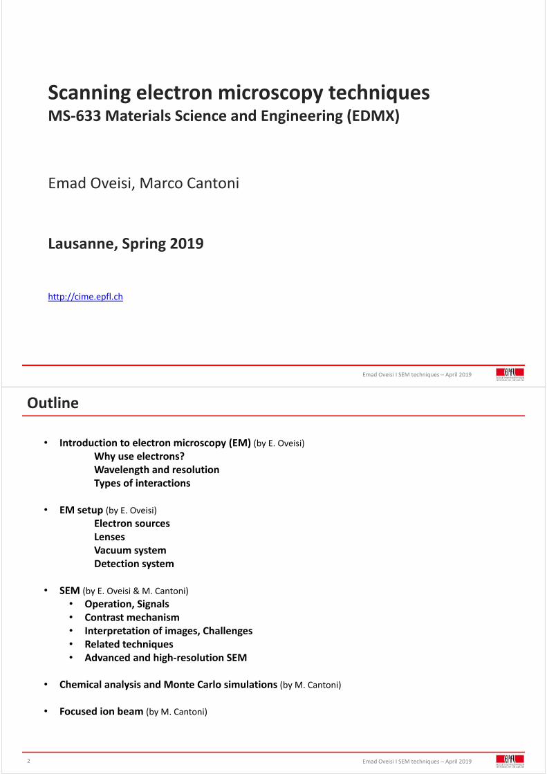
What is an electron microscope?
Emad Oveisi I SEM techniques – April 2019
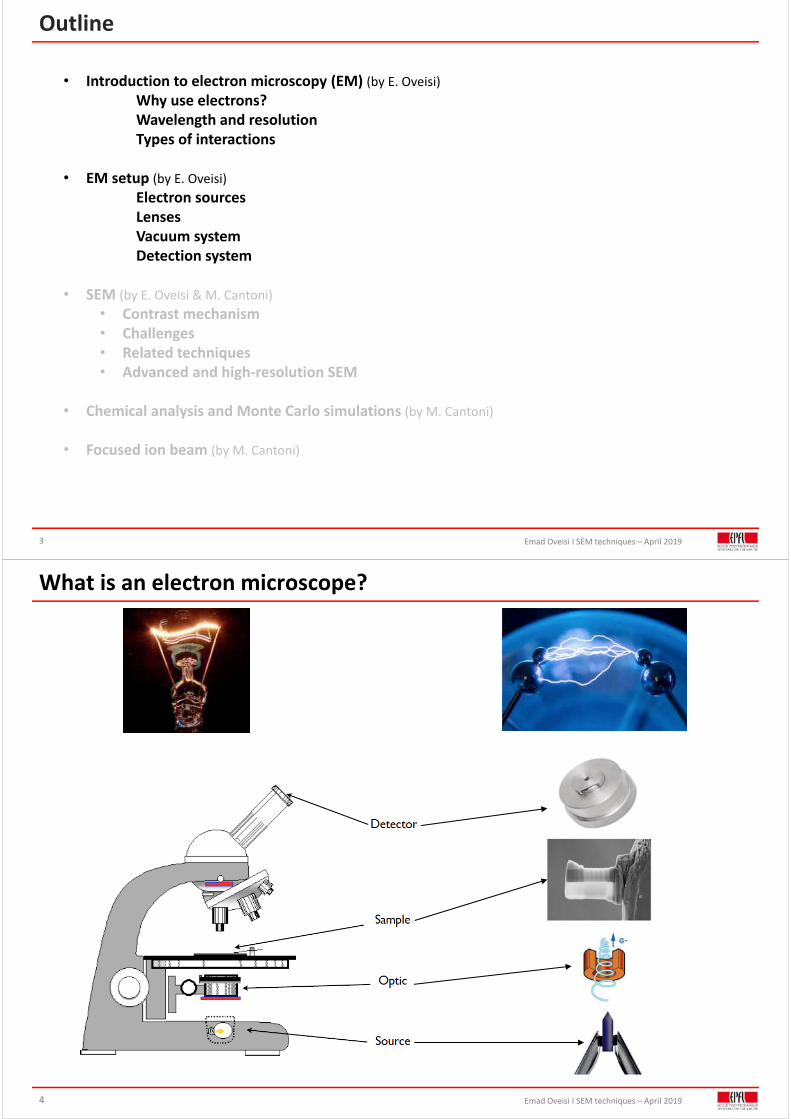
Why use electrons as probe?
5
1 cm 1 mm 100 µm 10 µm 1 µm 100 nm 10 nm 1 nm 0.1 nm
Naked eye
Conventional light microscopes
1 micron
40 micron
Size of an atom≈ 100 picometer
DNA helix
Electron microscopes
Electron wavelength: 0.0387 nm @ 1 keV0.0019 nm @ 300 keV
Developed by Ernst Ruska in 1931 (Nobel Prize in Physics 1986)Electrons have wave‐like properties (De Broglie 1924)The electron wavelength depends on its energy Magnetic lenses can be used to focus electrons
Visible light wavelength: 400‐700 nm
Emad Oveisi I SEM techniques – April 20196
Why use electrons as probe?
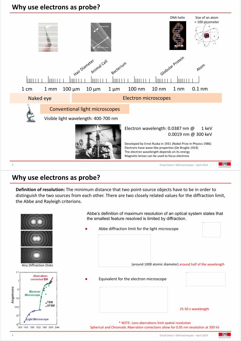
Definition of resolution: The minimum distance that two point‐source objects have to be in order to distinguish the two sources from each other. There are two closely related values for the diffraction limit, the Abbe and Rayleigh criterions.
Airy Diffraction Disks
● Abbe diffraction limit for the light microscope
The picture can't be displayed.
● Equivalent for the electron microscope
The picture can't be displayed.
The picture can't be displayed.
The picture can't be displayed.
* NOTE: Lens aberrations limit spatial resolutionSpherical and Chromatic Aberration corrections allow for 0.05 nm resolution at 300 kV
(around 1000 atomic diameter) around half of the wavelength
25‐50 x wavelength
Abbe’s definition of maximum resolution of an optical system states that the smallest feature resolved is limited by diffraction.
Emad Oveisi I SEM techniques – April 2019
Why use electrons as probe?
7
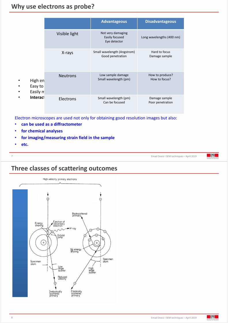
• High energy electrons have a short wavelength • Easy to produce high brightness electron beams • Easily manipulated ‐ focused• Interact strongly with matter
Advantageous Disadvantageous
Visible light Not very damagingEasily focusedEye detector
Long wavelengths (400 nm)
X‐rays Small wavelength (Angstrom)Good penetration
Hard to focusDamage sample
Neutrons Low sample damageSmall wavelength (pm)
How to produce?How to focus?
Electrons Small wavelength (pm)Can be focused
Damage samplePoor penetration
Electron microscopes are used not only for obtaining good resolution images but also:
• can be used as a diffractometer
• for chemical analyses
• for imaging/measuring strain field in the sample
• etc.
Emad Oveisi I SEM techniques – April 2019
Three classes of scattering outcomes
8
Emad Oveisi I SEM techniques – April 2019
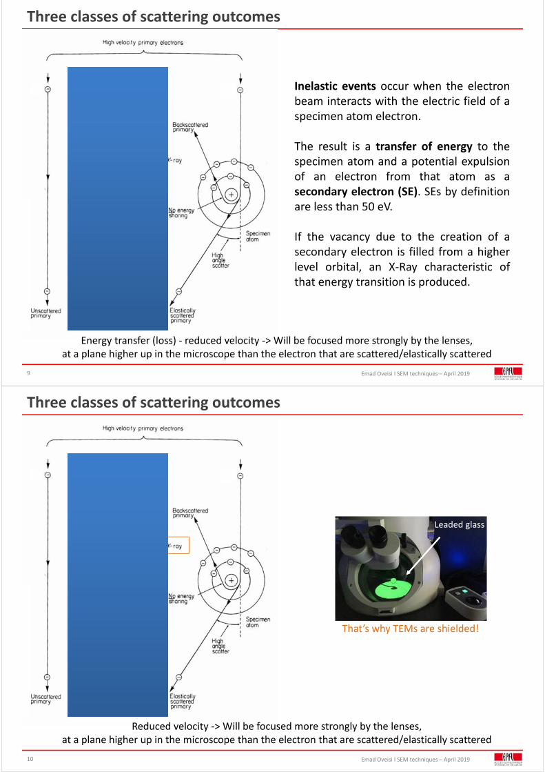
Three classes of scattering outcomes
9
Energy transfer (loss) ‐ reduced velocity ‐> Will be focused more strongly by the lenses,at a plane higher up in the microscope than the electron that are scattered/elastically scattered
Inelastic events occur when the electronbeam interacts with the electric field of aspecimen atom electron.
The result is a transfer of energy to thespecimen atom and a potential expulsionof an electron from that atom as asecondary electron (SE). SEs by definitionare less than 50 eV.
If the vacancy due to the creation of asecondary electron is filled from a higherlevel orbital, an X‐Ray characteristic ofthat energy transition is produced.
Emad Oveisi I SEM techniques – April 2019
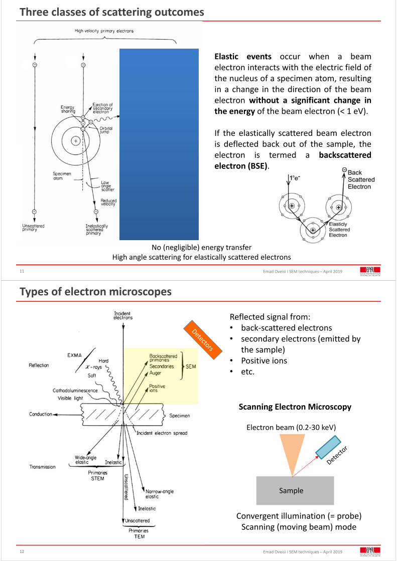
Reduced velocity ‐> Will be focused more strongly by the lenses,at a plane higher up in the microscope than the electron that are scattered/elastically scattered
Three classes of scattering outcomes
10
That’s why TEMs are shielded!
Leaded glass
Emad Oveisi I SEM techniques – April 2019
Three classes of scattering outcomes
11
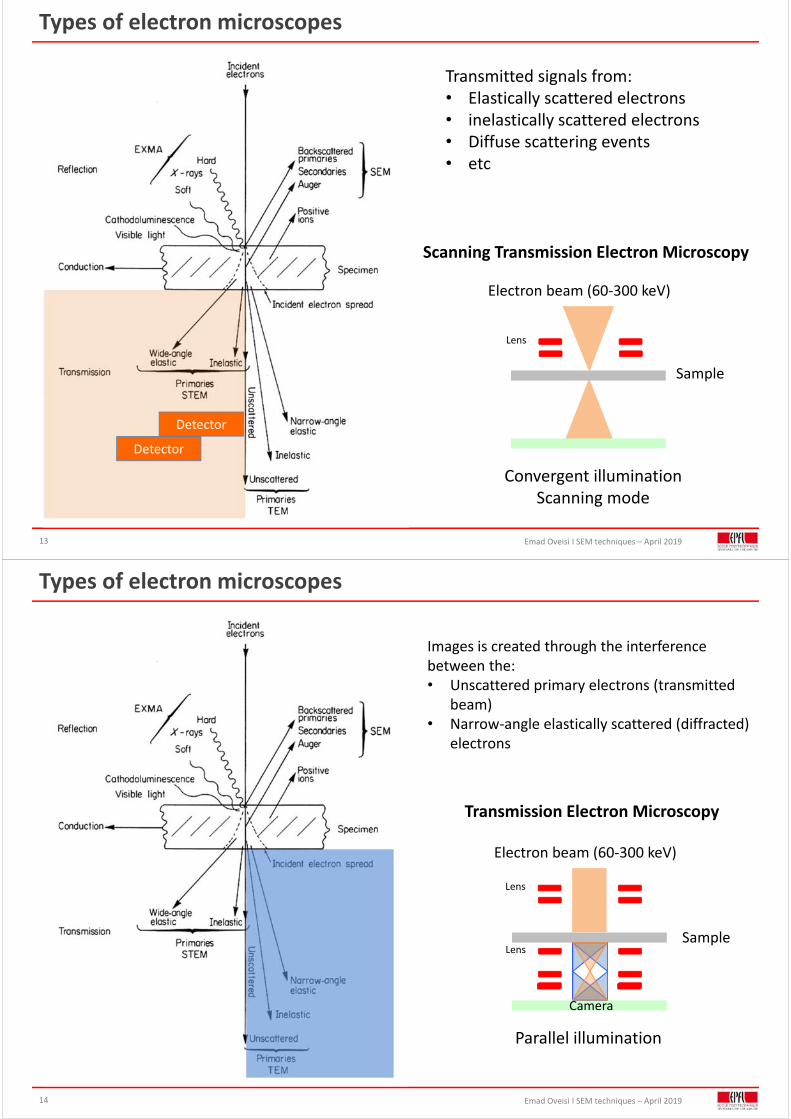
No (negligible) energy transferHigh angle scattering for elastically scattered electrons
Elastic events occur when a beamelectron interacts with the electric field ofthe nucleus of a specimen atom, resultingin a change in the direction of the beamelectron without a significant change inthe energy of the beam electron (< 1 eV).
If the elastically scattered beam electronis deflected back out of the sample, theelectron is termed a backscatteredelectron (BSE).
Emad Oveisi I SEM techniques – April 2019
Types of electron microscopes
12
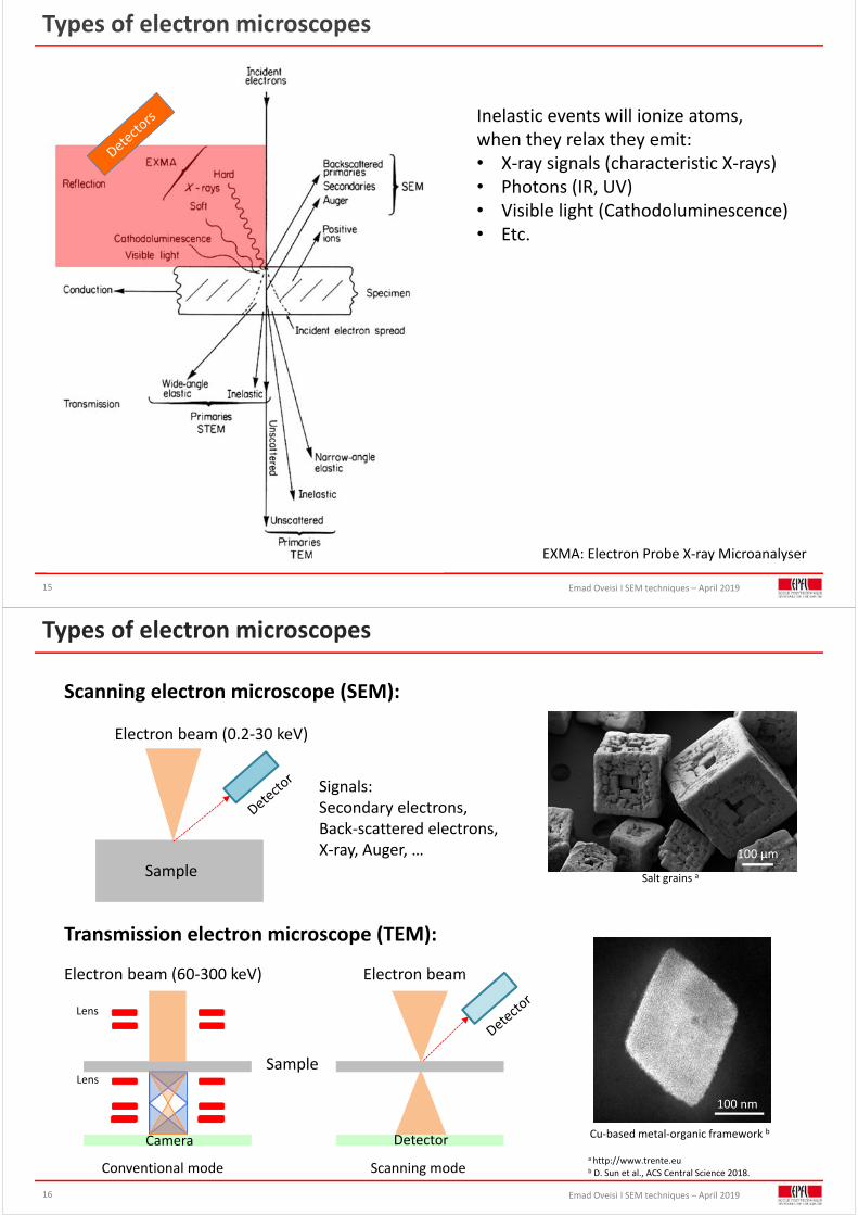
Reflected signal from:• back‐scattered electrons• secondary electrons (emitted by
the sample)• Positive ions• etc.
Electron beam (0.2‐30 keV)
Sample
Convergent illumination (= probe)Scanning (moving beam) mode
Scanning Electron Microscopy
Emad Oveisi I SEM techniques – April 2019
Transmitted signals from:• Elastically scattered electrons• inelastically scattered electrons• Diffuse scattering events• etc
Detector
Detector
Convergent illuminationScanning mode
Electron beam (60‐300 keV)
Sample
Lens
Types of electron microscopes
13
Scanning Transmission Electron Microscopy
Emad Oveisi I SEM techniques – April 201914
Electron beam (60‐300 keV)
Parallel illumination
Camera
Lens
Lens
Images is created through the interference between the:• Unscattered primary electrons (transmitted
beam)• Narrow‐angle elastically scattered (diffracted)
electrons
Sample
Types of electron microscopes
Transmission Electron Microscopy
Emad Oveisi I SEM techniques – April 201915
Inelastic events will ionize atoms,when they relax they emit:• X‐ray signals (characteristic X‐rays)• Photons (IR, UV)• Visible light (Cathodoluminescence)• Etc.
Types of electron microscopes
EXMA: Electron Probe X‐ray Microanalyser
Emad Oveisi I SEM techniques – April 2019
Types of electron microscopes
16
Electron beam (0.2‐30 keV)
Sample
Signals: Secondary electrons,Back‐scattered electrons, X‐ray, Auger, …
Scanning electron microscope (SEM):
Transmission electron microscope (TEM):
Electron beamElectron beam (60‐300 keV)
Sample
Detector
Conventional mode Scanning mode
100 µm
100 nm
Salt grains a
Cu‐based metal‐organic framework b
a http://www.trente.eub D. Sun et al., ACS Central Science 2018.
Camera
Lens
Lens
Emad Oveisi I SEM techniques – April 2019
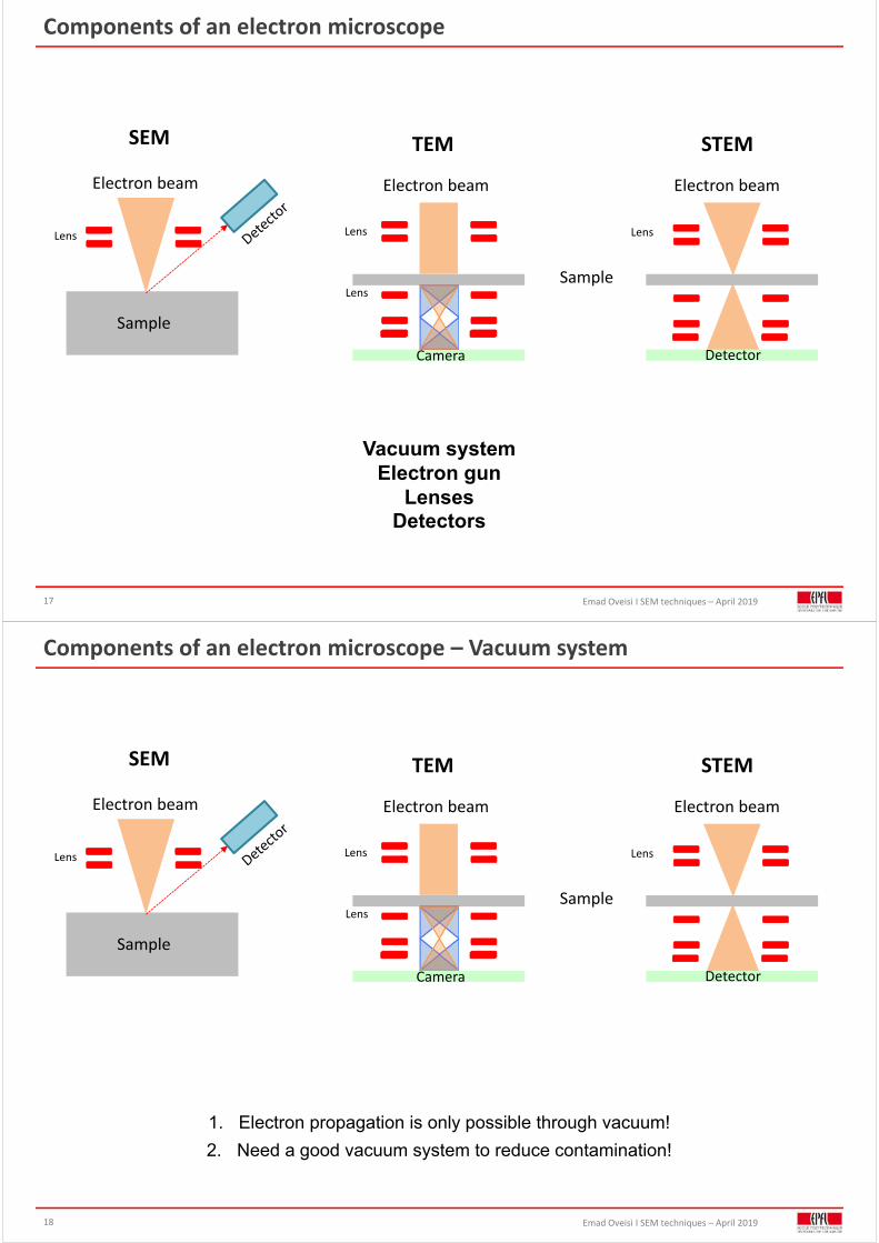
Components of an electron microscope
17
Electron beam
Sample
TEM
Electron beamElectron beam
Sample
DetectorCamera
Lens
Lens
SEM STEM
Lens Lens
Vacuum systemElectron gun
LensesDetectors
Emad Oveisi I SEM techniques – April 2019
Components of an electron microscope – Vacuum system
18
Electron beam
Sample
TEM
Electron beamElectron beam
Sample
DetectorCamera
Lens
Lens
SEM STEM
Lens Lens
1. Electron propagation is only possible through vacuum!
2. Need a good vacuum system to reduce contamination!
Emad Oveisi I SEM techniques – April 201919
Vacuum scale
To clean themicroscope room!
Primaryvacuum
Secondaryvacuum
Torr
Corse UHV(High vacuum) UHV
10‐1 10‐3 10‐6 10‐9760
Hoover, … Rotary vanepump
Oil diffusion pump
Turbomolecularpump
Ion getterpump
Different kinds of vacuum pumps have different range where they are effective
Emad Oveisi I SEM techniques – April 201920
• Primary vacuum (>0.1 Pa)
– Mechanical pump
• Secondary to high vacuum Detector or viewing chamber (<10-4 Pa)
– Oil diffusion pump
– Turbomolecular pump
• High and ultra-high vacuumGun & specimen area (<10-6 Pa)
– Ion getter pump
– Cold trapAirBuffer/
Reservoir Tank
EM Column
Detect Chamber
Gun Valve
Specimen exchange pump valve
Gun Ion Pump
Column Ion Pump
Electron Gun
Diffusion or TurbomolecularPump
Mechanical Rough Pump Vent Valve
Primary pump Valve
Detector Valve
Sample Holder
Column Valves
Vaccum level in space:1 Pa at 100km
above earth surface
Vacuum system

Emad Oveisi I SEM techniques – April 201921
Rotary vane pump
– Uses oil
– noisy
Vacuum system – Primary vacuum
Emad Oveisi I SEM techniques – April 201922
Oil diffusion pump
– Vibration free
– Contamination possible oil vapor
– High pumping capacity (>500 l/s)
– Best with cold trap
Vacuum system – Secondary vacuum

Emad Oveisi I SEM techniques – April 201923
Turbomolecular pump
– Rotation speed 20‐50’000 rpm
– Magnetic bearings
– Pumping volumes 50‐500 l/s
Vacuum system – Coarse UHV
Emad Oveisi I SEM techniques – April 2019
Vacuum system – Ultra‐high vacuum
24
Ion getter pump
– no vibrations
– No exit:improves vacuum !
Emad Oveisi I SEM techniques – April 2019
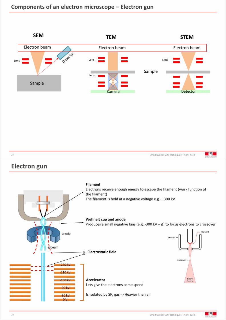
Components of an electron microscope – Electron gun
25
Electron beam
Sample
TEM
Electron beamElectron beam
Sample
DetectorCamera
Lens
Lens
SEM STEM
Lens Lens
Emad Oveisi I SEM techniques – April 2019
Electron gun
FilamentElectrons receive enough energy to escape the filament (work function of the filament)The filament is hold at a negative voltage e.g. – 300 kV
Wehnelt cup and anode Produces a small negative bias (e.g. ‐300 kV – Δ) to focus electrons to crossover
AcceleratorLets give the electrons some speed
Is isolated by SF4 gas ‐> Heavier than air
Electrostatic field
‐270 kV
‐210 kV
‐150 kV
‐90 kV
‐30 kV0 V
26
Emad Oveisi I SEM techniques – April 201927
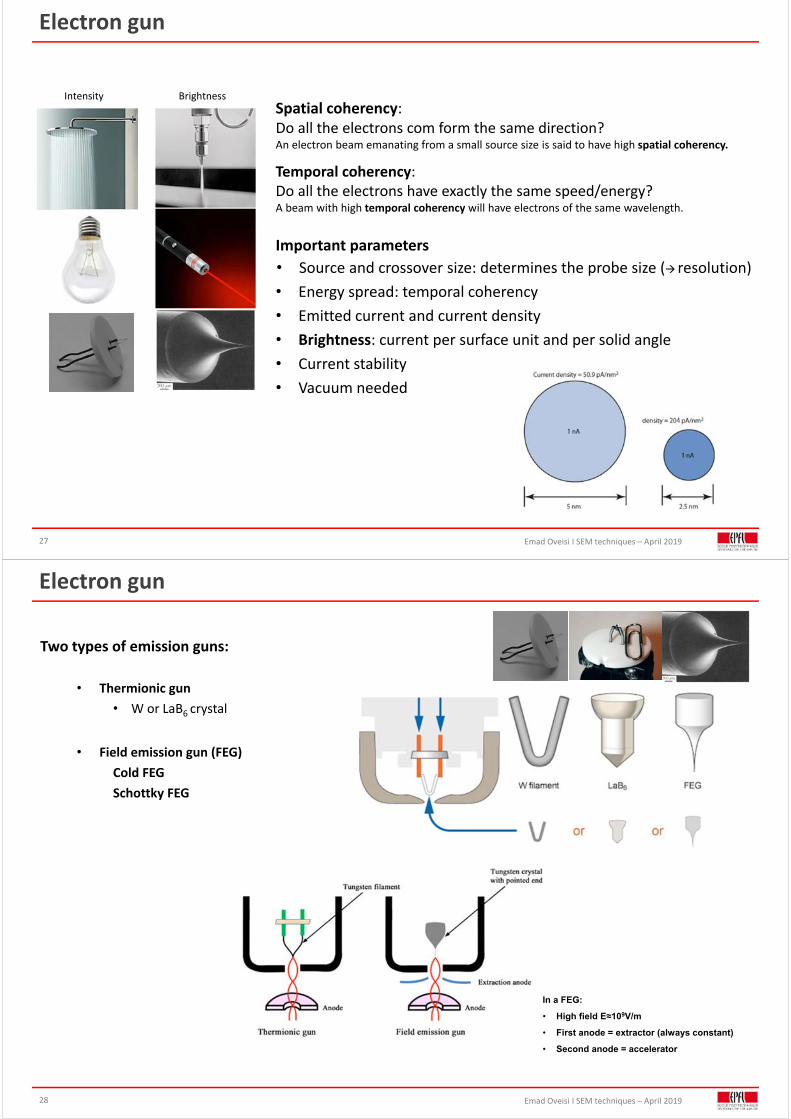
Intensity Brightness
Spatial coherency:Do all the electrons com form the same direction?An electron beam emanating from a small source size is said to have high spatial coherency.
Temporal coherency:Do all the electrons have exactly the same speed/energy?A beam with high temporal coherency will have electrons of the same wavelength.
Important parameters
• Source and crossover size: determines the probe size ( resolution)
• Energy spread: temporal coherency
• Emitted current and current density
• Brightness: current per surface unit and per solid angle
• Current stability
• Vacuum needed
Electron gun
Emad Oveisi I SEM techniques – April 201928
Two types of emission guns:
• Thermionic gun
• W or LaB6 crystal
• Field emission gun (FEG)
Cold FEG
Schottky FEG
Electron gun
In a FEG:
• High field E≈109V/m
• First anode = extractor (always constant)
• Second anode = accelerator
Emad Oveisi I SEM techniques – April 2019
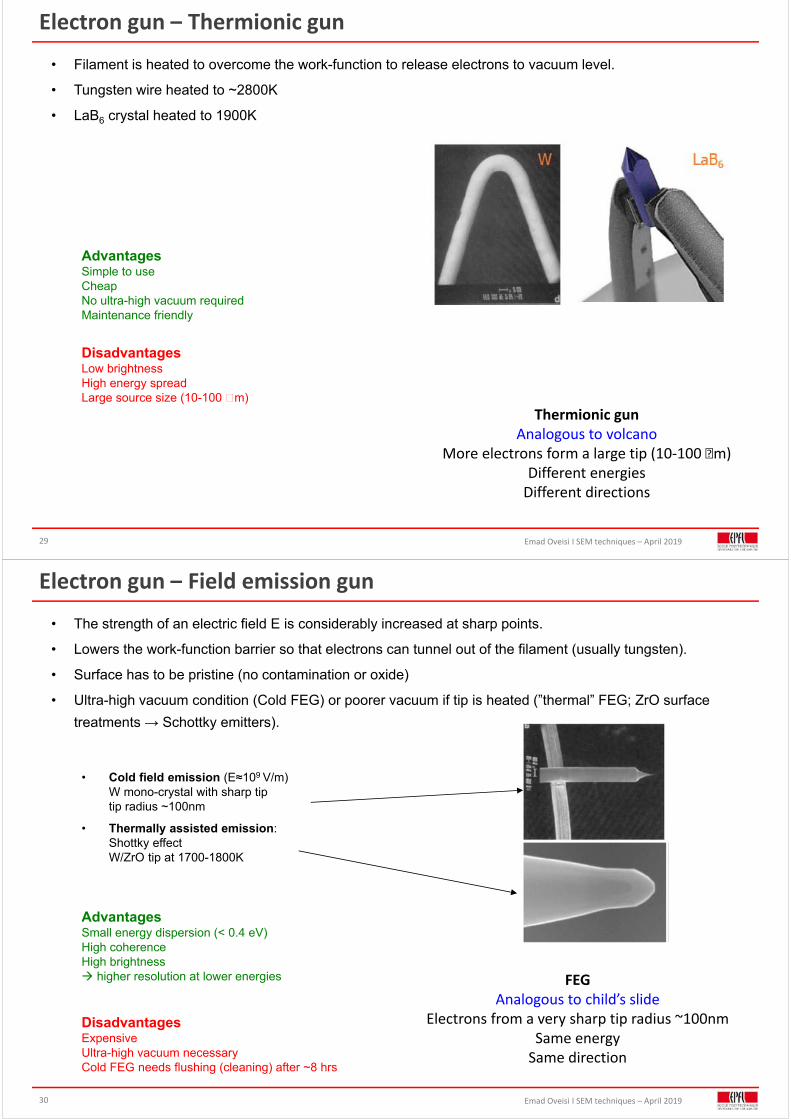
• Filament is heated to overcome the work-function to release electrons to vacuum level.
• Tungsten wire heated to ~2800K
• LaB6 crystal heated to 1900K
Electron gun – Thermionic gun
AdvantagesSimple to useCheapNo ultra-high vacuum required Maintenance friendly
DisadvantagesLow brightnessHigh energy spread Large source size (10-100 m)
Thermionic gunAnalogous to volcano
More electrons form a large tip (10‐100 m)Different energiesDifferent directions
29
Emad Oveisi I SEM techniques – April 2019
• The strength of an electric field E is considerably increased at sharp points.
• Lowers the work-function barrier so that electrons can tunnel out of the filament (usually tungsten).
• Surface has to be pristine (no contamination or oxide)
• Ultra-high vacuum condition (Cold FEG) or poorer vacuum if tip is heated (”thermal” FEG; ZrO surface
treatments → Schottky emitters).
Electron gun – Field emission gun
• Cold field emission (E≈109 V/m)W mono-crystal with sharp tiptip radius ~100nm
• Thermally assisted emission:Shottky effectW/ZrO tip at 1700-1800K
AdvantagesSmall energy dispersion (< 0.4 eV)High coherenceHigh brightness higher resolution at lower energies
DisadvantagesExpensiveUltra-high vacuum necessaryCold FEG needs flushing (cleaning) after ~8 hrs
FEGAnalogous to child’s slide
Electrons from a very sharp tip radius ~100nmSame energySame direction
30
Emad Oveisi I SEM techniques – April 2019
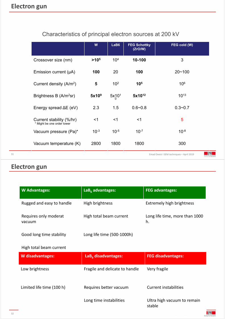
Characteristics of principal electron sources at 200 kV
W LaB6 FEG Schottky(ZrO/W)
FEG cold (W)
Crossover size (nm) >105 104 10-100 3
Emission current (µA) 100 20 100 20~100
Current density (A/m2) 5 102 105 106
Brightness B (A/m2sr) 5x10⁹ 5x10¹⁰
5x10¹² 1013
Energy spread ΔE (eV) 2.3 1.5 0.6~0.8 0.3~0.7
Current stability (%/hr) <1 <1 <1 5
Vacuum pressure (Pa)* 10-3 10-5 10-7 10-8
Vacuum temperature (K) 2800 1800 1800 300
* Might be one order lower
Electron gun
31
Emad Oveisi I SEM techniques – April 2019
W Advantages: LaB6 advantages: FEG advantages:
Rugged and easy to handle High brightness Extremely high brightness
Requires only moderat vacuum
High total beam current Long life time, more than 1000 h.
Good long time stability Long life time (500‐1000h)
High total beam current
W disadvantages: LaB6 disadvantages: FEG disadvantages:
Low brightness Fragile and delicate to handle Very fragile
Limited life time (100 h) Requires better vacuum Current instabilities
Long time instabilities Ultra high vacuum to remain stable
Electron gun
32
Emad Oveisi I SEM techniques – April 2019
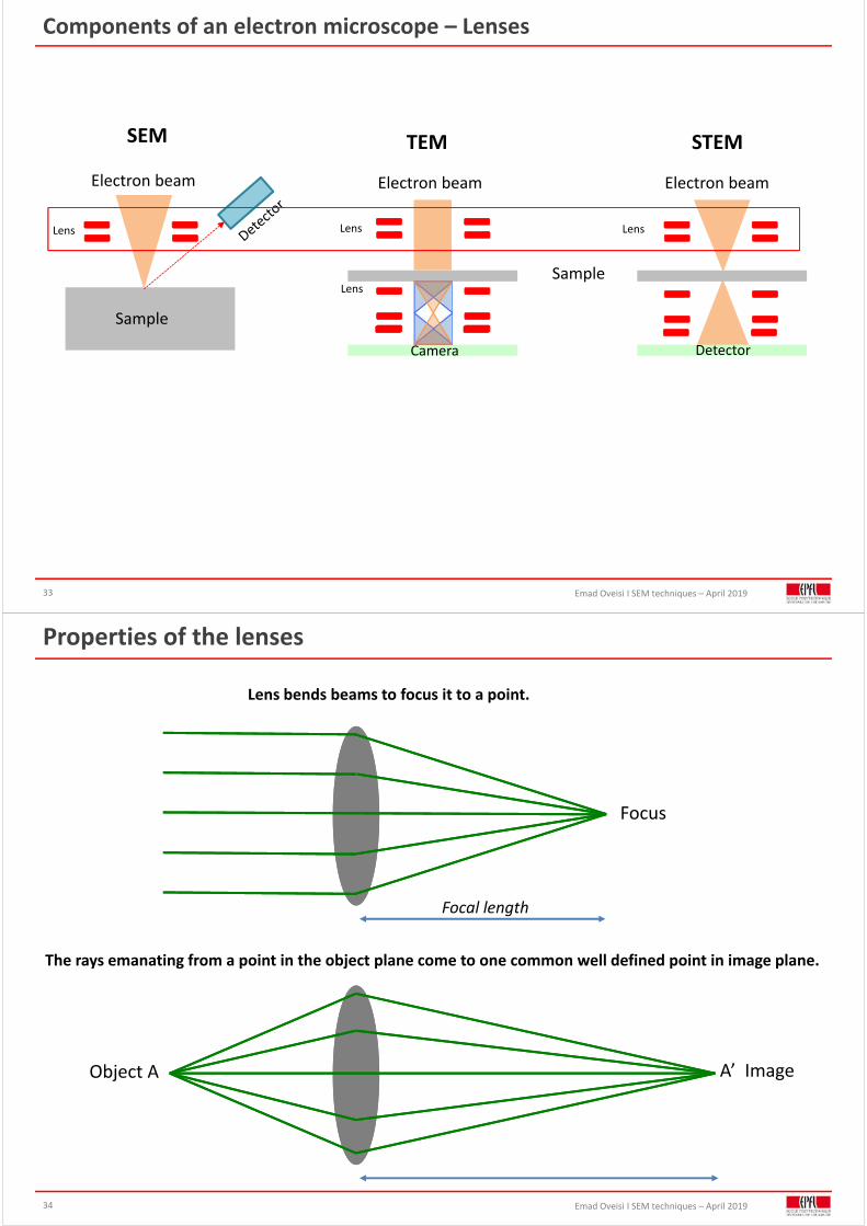
Components of an electron microscope – Lenses
33
Electron beam
Sample
TEM
Electron beamElectron beam
Sample
DetectorCamera
Lens
Lens
SEM STEM
Lens Lens
Emad Oveisi I SEM techniques – April 201934
Properties of the lenses
Lens bends beams to focus it to a point.
Focus
A’ ImageObject A
The rays emanating from a point in the object plane come to one common well defined point in image plane.
Focal length
Emad Oveisi I SEM techniques – April 201935
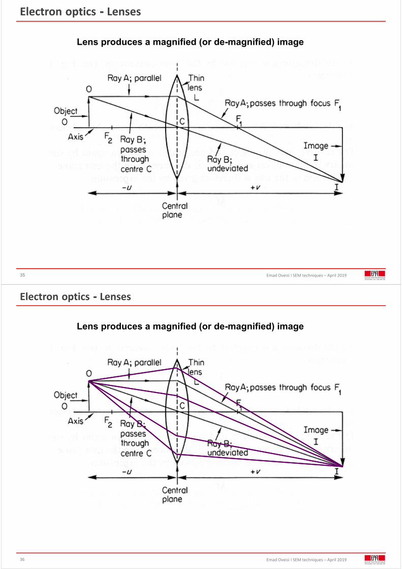
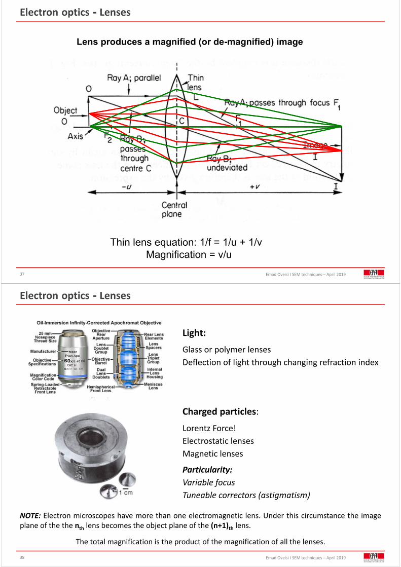
Lens produces a magnified (or de-magnified) image
Electron optics - Lenses
Emad Oveisi I SEM techniques – April 201936
Electron optics - Lenses
Lens produces a magnified (or de-magnified) image
Emad Oveisi I SEM techniques – April 201937
Electron optics - Lenses
Thin lens equation: 1/f = 1/u + 1/v Magnification = v/u
Lens produces a magnified (or de-magnified) image
Emad Oveisi I SEM techniques – April 201938
Light:
Glass or polymer lenses
Deflection of light through changing refraction index
Charged particles:
Lorentz Force!
Electrostatic lenses
Magnetic lenses
Particularity:
Variable focus
Tuneable correctors (astigmatism)
Electron optics - Lenses
NOTE: Electron microscopes have more than one electromagnetic lens. Under this circumstance the imageplane of the the nth lens becomes the object plane of the (n+1)th lens.
The total magnification is the product of the magnification of all the lenses.
Emad Oveisi I SEM techniques – April 201939
Magnetic field lines
B
V
Magnetic field lines
B
B
CurrentCurrent
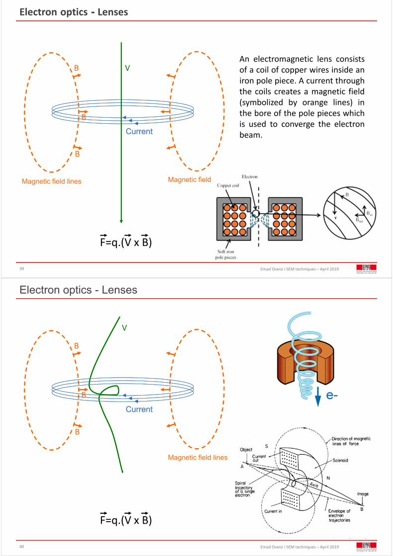
Electron optics - Lenses
An electromagnetic lens consistsof a coil of copper wires inside aniron pole piece. A current throughthe coils creates a magnetic field(symbolized by orange lines) inthe bore of the pole pieces whichis used to converge the electronbeam.
F=q.(V x B)
Emad Oveisi I SEM techniques – April 201940
B
V
Magnetic field lines
B
B
CurrentCurrent
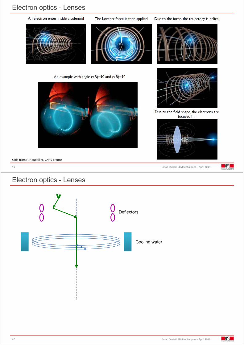
Electron optics - Lenses
F=q.(V x B)
Emad Oveisi I SEM techniques – April 201941
Slide from F. Houdellier, CNRS‐France
Electron optics - Lenses
Emad Oveisi I SEM techniques – April 201942
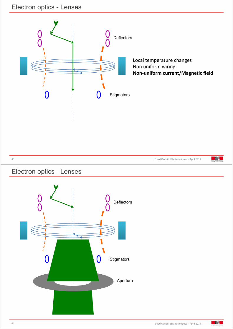
Deflectors
Cooling water
Electron optics - Lenses
Emad Oveisi I SEM techniques – April 201943
Deflectors
Stigmators
Local temperature changesNon uniform wiringNon‐uniform current/Magnetic field
Electron optics - Lenses
Emad Oveisi I SEM techniques – April 201944
Deflectors
Stigmators
Aperture
Electron optics - Lenses
Emad Oveisi I SEM techniques – April 201945
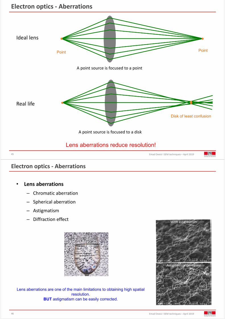
A point source is focused to a point
A point source is focused to a disk
Ideal lens
Real life
Lens aberrations reduce resolution!
Disk of least confusion
PointPoint
Electron optics ‐ Aberrations
Emad Oveisi I SEM techniques – April 2019
With astigmatism
Astigmatism corrected
Electron optics ‐ Aberrations
46
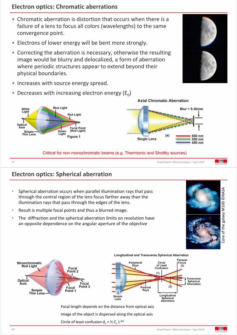
Lens aberrations are one of the main limitations to obtaining high spatial resolution.
BUT astigmatism can be easily corrected.
• Lens aberrations
– Chromatic aberration
– Spherical aberration
– Astigmatism
– Diffraction effect
Emad Oveisi I SEM techniques – April 2019
Electron optics: Chromatic aberrations
47
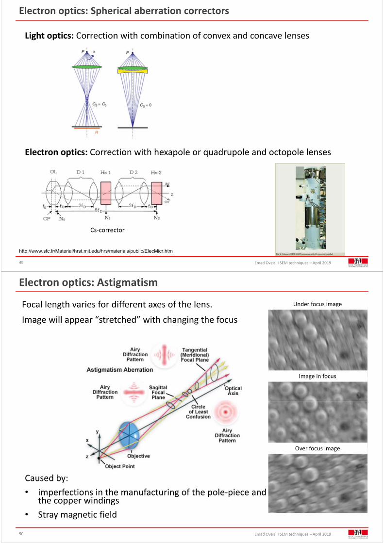
Critical for non-monochromatic beams (e.g. Thermionic and Shottky sources)
• Chromatic aberration is distortion that occurs when there is a failure of a lens to focus all colors (wavelengths) to the same convergence point.
• Electrons of lower energy will be bent more strongly.
• Correcting the aberration is necessary, otherwise the resulting image would be blurry and delocalized, a form of aberration where periodic structures appear to extend beyond their physical boundaries.
• Increases with source energy spread.
• Decreases with increasing electron energy (E0)
Emad Oveisi I SEM techniques – April 2019
Electron optics: Spherical aberration
48
Focal length depends on the distance from optical axis
Image of the object is dispersed along the optical axis
Circle of least confusion ds = ½ Cs 3ar
• Spherical aberration occurs when parallel illumination rays that pass through the central region of the lens focus farther away than the illumination rays that pass through the edges of the lens.
• Result is multiple focal points and thus a blurred image.
• The diffraction and the spherical aberration limits on resolution have an opposite dependence on the angular aperture of the objective
Core of the galaxy M
100 ©
NASA
Emad Oveisi I SEM techniques – April 2019
Light optics: Correction with combination of convex and concave lenses
Electron optics: Correction with hexapole or quadrupole and octopole lenses
Electron optics: Spherical aberration correctors
49
http://www.sfc.fr/Material/hrst.mit.edu/hrs/materials/public/ElecMicr.htm
Cs‐corrector
Emad Oveisi I SEM techniques – April 2019
Electron optics: Astigmatism
50
Focal length varies for different axes of the lens.
Image will appear “stretched” with changing the focus
Under focus image
Image in focus
Over focus image
Caused by:
• imperfections in the manufacturing of the pole‐piece and the copper windings
• Stray magnetic field
Emad Oveisi I SEM techniques – April 2019
Light optics: correction with cylindrical lenses
Electron optics: Correction with quadrupole lenses2 quadrupole lenses under 45 degree allow to control strength and direction of correction
Electron optics: Astigmators
51
+
+
+
+‐
‐
‐‐
Emad Oveisi I SEM techniques – April 201952
Electron optics: Astigmatism
With astigmatism Astigmatism corrected
Emad Oveisi I SEM techniques – April 201953
Electron optics: Aberrations
Spherical aberration
Chromatic aberration
Astigmatism
Spherical aberration
Lateralchromatic aberration
Sagittal astigmatismMeridional astigmatism
Longitudinalchromatic aberration
Emad Oveisi I SEM techniques – April 201954
Electron optics ‐ Aberrations
The diffraction and the spherical aberration limits on resolution have an opposite dependence on the angular aperture of the objective lens.
Emad Oveisi I SEM techniques – April 201955
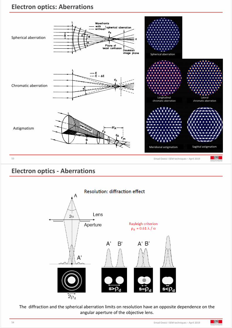
Optimal Aperture size (30µm) Large Aperture size (120µm)
Though large apertures produce larger convergence angles (less diffraction effect), spherical aberration increases probe size and reduces resolution
Electron optics ‐ Aberrations
Emad Oveisi I SEM techniques – April 2019
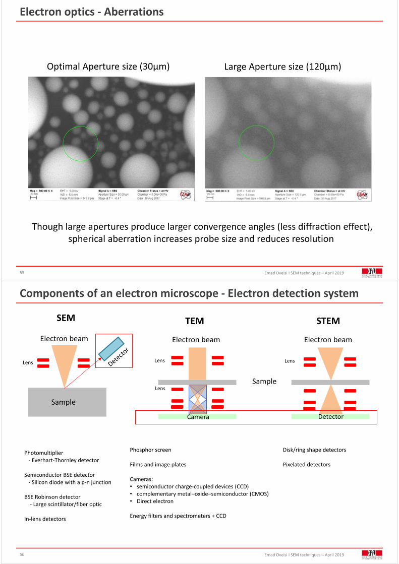
Components of an electron microscope ‐ Electron detection system
56
Electron beam
Sample
TEM
Electron beamElectron beam
Sample
DetectorCamera
Lens
Lens
SEM STEM
Photomultiplier‐ Everhart‐Thornley detector
Semiconductor BSE detector‐ Silicon diode with a p‐n junction
BSE Robinson detector‐ Large scintillator/fiber optic
In‐lens detectors
Phosphor screen
Films and image plates
Cameras:• semiconductor charge‐coupled devices (CCD)• complementary metal–oxide–semiconductor (CMOS)• Direct electron
Energy filters and spectrometers + CCD
Disk/ring shape detectors
Pixelated detectors
Lens Lens
Emad Oveisi I SEM techniques – April 201957
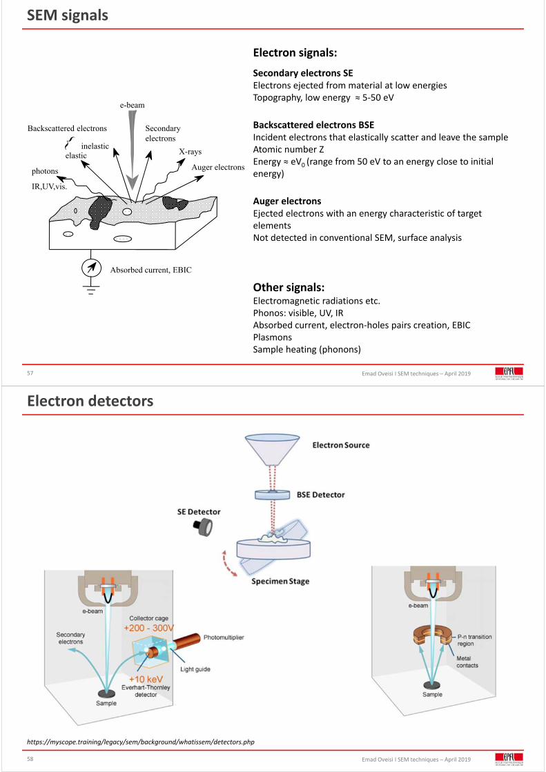
SEM signals
X-rayselasticinelastic
Backscattered electrons
e-beam
Secondaryelectrons
photons Auger electrons
IR,UV,vis.
Absorbed current, EBIC
Electron signals:
Secondary electrons SEElectrons ejected from material at low energiesTopography, low energy ≈ 5‐50 eV
Backscattered electrons BSEIncident electrons that elastically scatter and leave the sampleAtomic number ZEnergy ≈ eV0 (range from 50 eV to an energy close to initial energy)
Auger electronsEjected electrons with an energy characteristic of target elementsNot detected in conventional SEM, surface analysis
Other signals:Electromagnetic radiations etc.Phonos: visible, UV, IRAbsorbed current, electron‐holes pairs creation, EBICPlasmonsSample heating (phonons)
Emad Oveisi I SEM techniques – April 201958
Electron detectors
https://myscope.training/legacy/sem/background/whatissem/detectors.php
Emad Oveisi I SEM techniques – April 201959
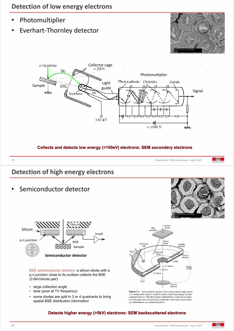
Detection of low energy electrons
Collects and detects low energy (<100eV) electrons: SEM secondary electronsCollects and detects low energy (<100eV) electrons: SEM secondary electrons
• Photomultiplier
• Everhart‐Thornley detector
Sample
Collector cage
Photomultiplier
Signal
Light guide
Scintillator
Emad Oveisi I SEM techniques – April 201960
Detection of high energy electrons
• Semiconductor detector
BSE semiconductor detector: a silicon diode with a p-n junction close to its surface collects the BSE (3.8eV/ehole pair)
• large collection angle• slow (poor at TV frequency)
• some diodes are split in 2 or 4 quadrants to bring spatial BSE distribution information
Detects higher energy (>5kV) electrons: SEM backscattered electronsDetects higher energy (>5kV) electrons: SEM backscattered electrons
Semiconductor detector
Silicon
p‐n junction
Sample


![Cold-Cathode Kiloampere Electron Gun with Secondary ... · experiments with magnetrons in secondary emission mode [6]. The secondary emission current pulse has shorter rise time than](https://img.pdfslide.us/doc/110x75/5f1672843c02743f560f57e6/cold-cathode-kiloampere-electron-gun-with-secondary-experiments-with-magnetrons.jpg)