Embed Size (px)
Citation preview
Materials Science and Engineering B69–70 (2000) 243–246
Scaling law and dynamical exponent in the Volmer–Weber growthmode: silver on GaAs(001)2×4
E. Placidi *, M. Fanfoni, F. Arciprete, F. Patella, N. Motta, A. BalzarottiIstituto Nazionale per la Fisica della Materia and Dipartimento di Fisica, Uni6ersita di Roma ‘Tor Vergata’, Via della Ricerca Scientifica 1,
00133 Rome, Italy
Abstract
The growth of Ag deposited onto the GaAs(001)2×4 has been investigated by means of scanning tunnelling microscopy. Silverforms islands (Volmer–Weber growth) whose average dimension increases according to U1/z (with z=4.2), U being the numberof Ag atoms deposited at constant rate onto GaAs. The Ag islands exhibit a hut shape with {210} and {310} facets. The kineticof surface coverage has been measured and the Avrami exponent, n, has been determined, finding n=0.61. Both z and n arerelated to the dynamic nature of the growth process. © 2000 Elsevier Science S.A. All rights reserved.
Keywords: STM; Volmer–Weber; GaAs; Scaling Law; Avrami
www.elsevier.com/locate/mseb
1. Introduction
We investigate the formation of the Ag/GaAs(001)2×4 interface through scanning tunnellingmicroscopy (STM) and report new results concerningthe morphology of the silver film during its growth atroom temperature. In previous studies of this interface[1] we concentrated on its differences relative to Ag/GaAs(110) concerning the evolution of the electronicstates during the junction formation and the morphol-ogy of growth of the metal. We made use of high-reso-lution electron energy loss spectroscopy (HREELS),X-ray photoelectron spectroscopy (XPS) and STM. Asfar as the morphology is concerned, both interfaces arecharacterised by a Volmer–Weber mode of growth, butislands exhibit significant differences in terms of shape,size and number per unit surface. Here we extend therange of Ag coverages studying in more detail, by STM,the kinetics of the surface up to a covering fractionS=0.60. In particular we paid attention to the average-island growth discovering the remarkable fact that thelaw of growth has a power form, namely �r�:U14,where �r� is the mean radius of the islands and U isamount of silver deposited, at constant rate, onto thesubstrate. By matching these data with those obtainedby XPS, we improve the previous result [1] on thekinetics of the film growth, and determine the Avrami’s
exponent. Moreover we evidence the formation of hut-shaped silver crystallites for nominal thickness largerthan 2 A, . At variance with those formed on theGaAs(110), which exhibit {111} facets [2], these crystal-lites develop {210} and/or {310} facets, depending onthe orientation of the longer side and of the basal plane(001) or (110) of the island.
2. Results and discussion
The GaAs(001) was grown by the MBE technique,capped with arsenic and then moved into the analysischamber. The experimental set up and the substratepreparation are the same as described in [1]. Silver wasevaporated from a tungsten basket at a rate of 1 A, /min.During evaporation the pressure in the chamber was inthe range 10−10 mbar and the substrate was held atroom temperature.
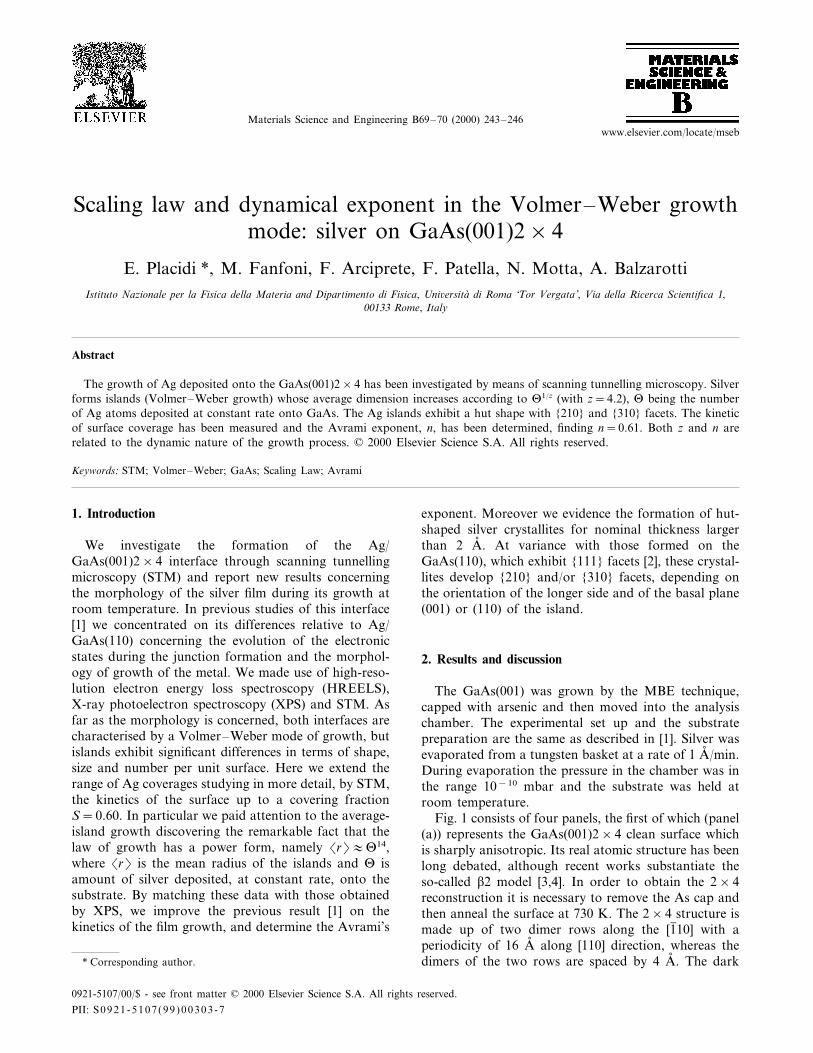
Fig. 1 consists of four panels, the first of which (panel(a)) represents the GaAs(001)2×4 clean surface whichis sharply anisotropic. Its real atomic structure has beenlong debated, although recent works substantiate theso-called b2 model [3,4]. In order to obtain the 2×4reconstruction it is necessary to remove the As cap andthen anneal the surface at 730 K. The 2×4 structure ismade up of two dimer rows along the [1( 10] with aperiodicity of 16 A, along [110] direction, whereas thedimers of the two rows are spaced by 4 A, . The dark* Corresponding author.
0921-5107/00/$ - see front matter © 2000 Elsevier Science S.A. All rights reserved.
PII: S0921 -5107 (99 )00303 -7
E. Placidi et al. / Materials Science and Engineering B69–70 (2000) 243–246244
Fig. 1. STM filled states images for the GaAs(001)2×4 surface versus Ag coverage: (a) 60×60 nm2 of clean surface, (b) 50×50 nm2 image at1 ML of Ag coverage, (c) 70×70 nm2 image at 2 ML of Ag coverage, (d) 60×60 nm2 image at 6 ML of Ag coverage.
lines are two missing As rows which lay, with respect tothe bright one, two atomic planes (As plus Ga) below,along the normal to the surface. Surface steps do notinfluence the nuclei distribution.
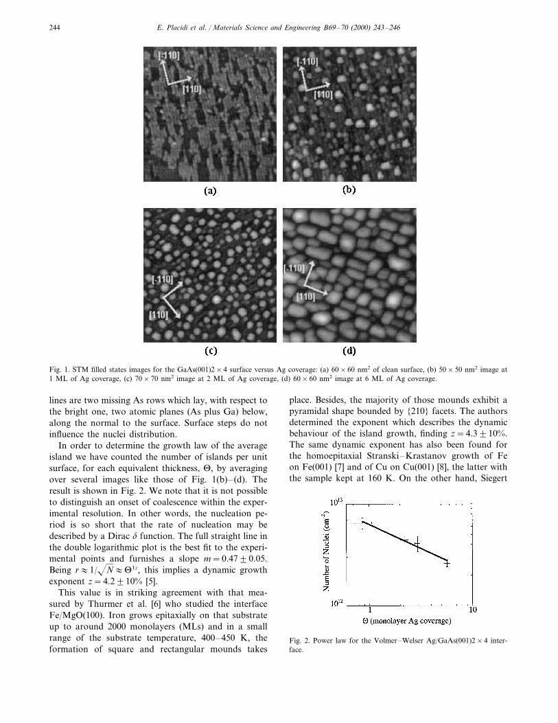
In order to determine the growth law of the averageisland we have counted the number of islands per unitsurface, for each equivalent thickness, U, by averagingover several images like those of Fig. 1(b)–(d). Theresult is shown in Fig. 2. We note that it is not possibleto distinguish an onset of coalescence within the exper-imental resolution. In other words, the nucleation pe-riod is so short that the rate of nucleation may bedescribed by a Dirac d function. The full straight line inthe double logarithmic plot is the best fit to the experi-mental points and furnishes a slope m=0.4790.05.Being r:1/N:U1z, this implies a dynamic growthexponent z=4.2910% [5].
This value is in striking agreement with that mea-sured by Thurmer et al. [6] who studied the interfaceFe/MgO(100). Iron grows epitaxially on that substrateup to around 2000 monolayers (MLs) and in a smallrange of the substrate temperature, 400–450 K, theformation of square and rectangular mounds takes
place. Besides, the majority of those mounds exhibit apyramidal shape bounded by {210} facets. The authorsdetermined the exponent which describes the dynamicbehaviour of the island growth, finding z=4.3910%.The same dynamic exponent has also been found forthe homoepitaxial Stranski–Krastanov growth of Feon Fe(001) [7] and of Cu on Cu(001) [8], the latter withthe sample kept at 160 K. On the other hand, Siegert
Fig. 2. Power law for the Volmer–Welser Ag/GaAs(001)2×4 inter-face.
E. Placidi et al. / Materials Science and Engineering B69–70 (2000) 243–246 245
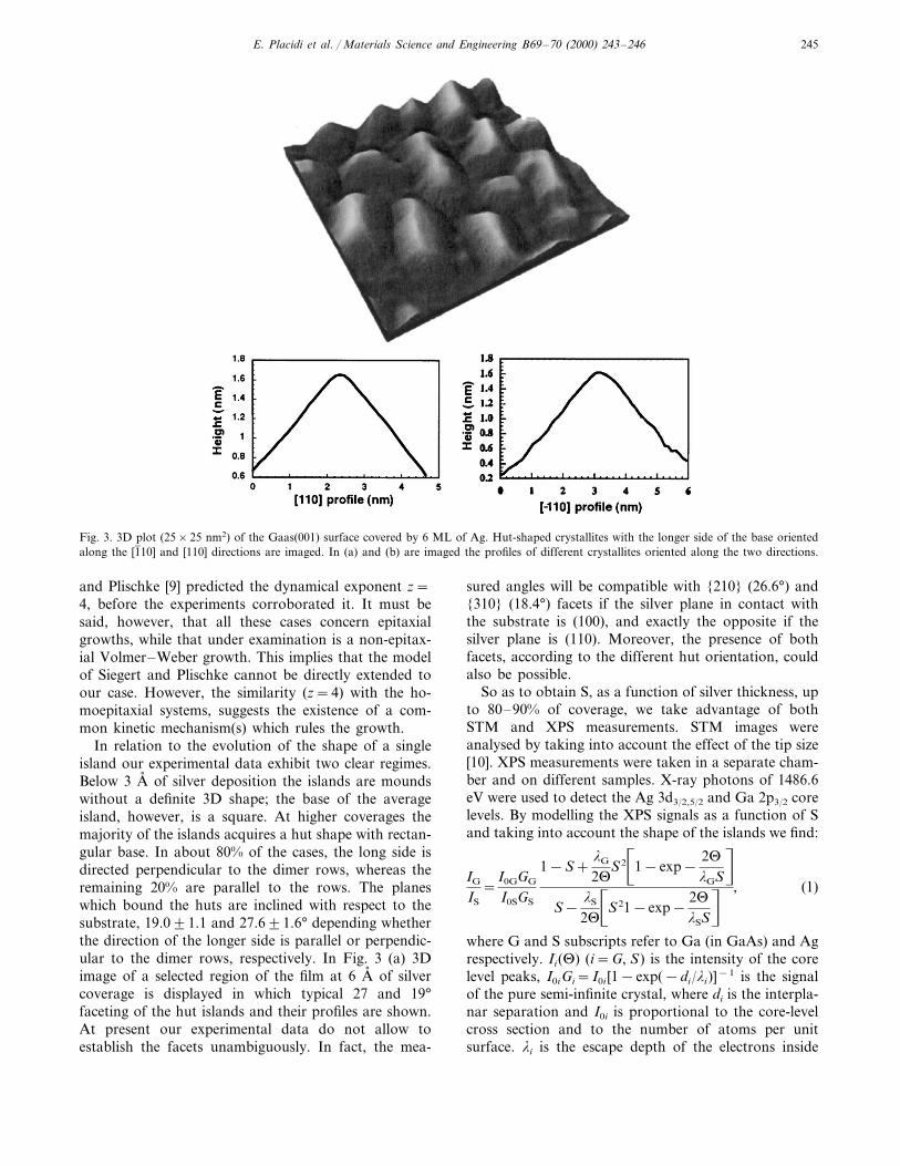
Fig. 3. 3D plot (25×25 nm2) of the Gaas(001) surface covered by 6 ML of Ag. Hut-shaped crystallites with the longer side of the base orientedalong the [1( 10] and [110] directions are imaged. In (a) and (b) are imaged the profiles of different crystallites oriented along the two directions.
and Plischke [9] predicted the dynamical exponent z=4, before the experiments corroborated it. It must besaid, however, that all these cases concern epitaxialgrowths, while that under examination is a non-epitax-ial Volmer–Weber growth. This implies that the modelof Siegert and Plischke cannot be directly extended toour case. However, the similarity (z=4) with the ho-moepitaxial systems, suggests the existence of a com-mon kinetic mechanism(s) which rules the growth.
In relation to the evolution of the shape of a singleisland our experimental data exhibit two clear regimes.Below 3 A, of silver deposition the islands are moundswithout a definite 3D shape; the base of the averageisland, however, is a square. At higher coverages themajority of the islands acquires a hut shape with rectan-gular base. In about 80% of the cases, the long side isdirected perpendicular to the dimer rows, whereas theremaining 20% are parallel to the rows. The planeswhich bound the huts are inclined with respect to thesubstrate, 19.091.1 and 27.691.6° depending whetherthe direction of the longer side is parallel or perpendic-ular to the dimer rows, respectively. In Fig. 3 (a) 3Dimage of a selected region of the film at 6 A, of silvercoverage is displayed in which typical 27 and 19°faceting of the hut islands and their profiles are shown.At present our experimental data do not allow toestablish the facets unambiguously. In fact, the mea-
sured angles will be compatible with {210} (26.6°) and{310} (18.4°) facets if the silver plane in contact withthe substrate is (100), and exactly the opposite if thesilver plane is (110). Moreover, the presence of bothfacets, according to the different hut orientation, couldalso be possible.
So as to obtain S, as a function of silver thickness, upto 80–90% of coverage, we take advantage of bothSTM and XPS measurements. STM images wereanalysed by taking into account the effect of the tip size[10]. XPS measurements were taken in a separate cham-ber and on different samples. X-ray photons of 1486.6eV were used to detect the Ag 3d3/2,5/2 and Ga 2p3/2 corelevels. By modelling the XPS signals as a function of Sand taking into account the shape of the islands we find:
IG
IS
=I0GGG
I0SGS
1−S+lG
2US2�1−exp−
2UlGS
nS−
lS
2U�
S21−exp−2UlSS
n , (1)
where G and S subscripts refer to Ga (in GaAs) and Agrespectively. Ii(U) (i=G, S) is the intensity of the corelevel peaks, I0iGi=I0i [1−exp(−di/li)]−1 is the signalof the pure semi-infinite crystal, where di is the interpla-nar separation and I0i is proportional to the core-levelcross section and to the number of atoms per unitsurface. li is the escape depth of the electrons inside
E. Placidi et al. / Materials Science and Engineering B69–70 (2000) 243–246246
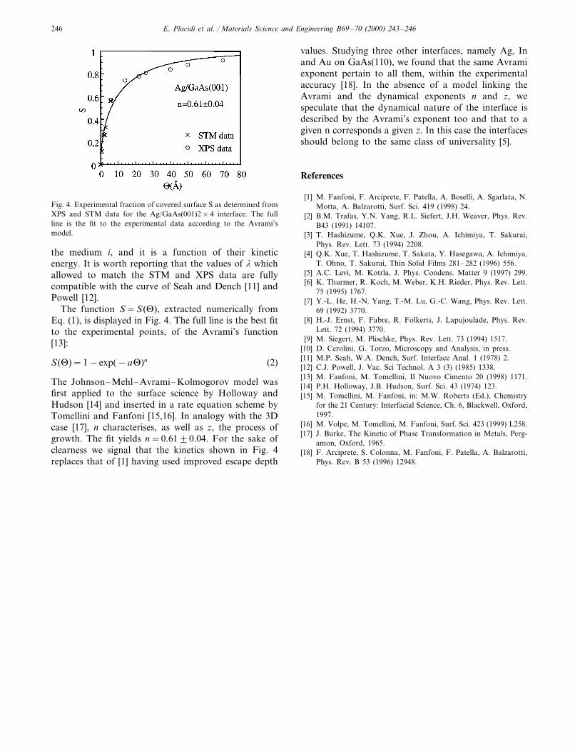
Fig. 4. Experimental fraction of covered surface S as determined fromXPS and STM data for the Ag/GaAs(001)2×4 interface. The fullline is the fit to the experimental data according to the Avrami’smodel.
values. Studying three other interfaces, namely Ag, Inand Au on GaAs(110), we found that the same Avramiexponent pertain to all them, within the experimentalaccuracy [18]. In the absence of a model linking theAvrami and the dynamical exponents n and z, wespeculate that the dynamical nature of the interface isdescribed by the Avrami’s exponent too and that to agiven n corresponds a given z. In this case the interfacesshould belong to the same class of universality [5].
References
[1] M. Fanfoni, F. Arciprete, F. Patella, A. Boselli, A. Sgarlata, N.Motta, A. Balzarotti, Surf. Sci. 419 (1998) 24.
[2] B.M. Trafas, Y.N. Yang, R.L. Siefert, J.H. Weaver, Phys. Rev.B43 (1991) 14107.
[3] T. Hashizume, Q.K. Xue, J. Zhou, A. Ichimiya, T. Sakurai,Phys. Rev. Lett. 73 (1994) 2208.
[4] Q.K. Xue, T. Hashizume, T. Sakata, Y. Hasegawa, A. Ichimiya,T. Ohno, T. Sakurai, Thin Solid Films 281–282 (1996) 556.
[5] A.C. Levi, M. Kotrla, J. Phys. Condens. Matter 9 (1997) 299.[6] K. Thurmer, R. Koch, M. Weber, K.H. Rieder, Phys. Rev. Lett.
75 (1995) 1767.[7] Y.-L. He, H.-N. Yang, T.-M. Lu, G.-C. Wang, Phys. Rev. Lett.
69 (1992) 3770.[8] H.-J. Ernst, F. Fabre, R. Folkerts, J. Lapujoulade, Phys. Rev.
Lett. 72 (1994) 3770.[9] M. Siegert, M. Plischke, Phys. Rev. Lett. 73 (1994) 1517.
[10] D. Cerolini, G. Torzo, Microscopy and Analysis, in press.[11] M.P. Seah, W.A. Dench, Surf. Interface Anal. 1 (1978) 2.[12] C.J. Powell, J. Vac. Sci Technol. A 3 (3) (1985) 1338.[13] M. Fanfoni, M. Tomellini, Il Nuovo Cimento 20 (1998) 1171.[14] P.H. Holloway, J.B. Hudson, Surf. Sci. 43 (1974) 123.[15] M. Tomellini, M. Fanfoni, in: M.W. Roberts (Ed.), Chemistry
for the 21 Century: Interfacial Science, Ch. 6, Blackwell, Oxford,1997.
[16] M. Volpe, M. Tomellini, M. Fanfoni, Surf. Sci. 423 (1999) L258.[17] J. Burke, The Kinetic of Phase Transformation in Metals, Perg-
amon, Oxford, 1965.[18] F. Arciprete, S. Colonna, M. Fanfoni, F. Patella, A. Balzarotti,
Phys. Rev. B 53 (1996) 12948.
the medium i, and it is a function of their kineticenergy. It is worth reporting that the values of l whichallowed to match the STM and XPS data are fullycompatible with the curve of Seah and Dench [11] andPowell [12].
The function S=S(U), extracted numerically fromEq. (1), is displayed in Fig. 4. The full line is the best fitto the experimental points, of the Avrami’s function[13]:
S(U)=1−exp(−aU)n (2)
The Johnson–Mehl–Avrami–Kolmogorov model wasfirst applied to the surface science by Holloway andHudson [14] and inserted in a rate equation scheme byTomellini and Fanfoni [15,16]. In analogy with the 3Dcase [17], n characterises, as well as z, the process ofgrowth. The fit yields n=0.6190.04. For the sake ofclearness we signal that the kinetics shown in Fig. 4replaces that of [1] having used improved escape depth
.