Embed Size (px)
Citation preview
Organic Electronics 15 (2014) 1229–1234
Contents lists available at ScienceDirect
Organic Electronics
journal homepage: www.elsevier .com/locate /orgel
Scaling down of organic complementary logic gatesfor compact logic on foil
http://dx.doi.org/10.1016/j.orgel.2014.03.0231566-1199/� 2014 Published by Elsevier B.V.
⇑ Corresponding author. Tel.: +32 16281062.E-mail address: [email protected] (T.-H. Ke).
Tung-Huei Ke a,⇑, Robert Müller a, Benjamin Kam a,b, Maarten Rockele a,b, Adrian Chasin a,b,Kris Myny a, Soeren Steudel a, Wibren D. Oosterbaan c, Laurence Lutsen c, Jan Genoe a,Linda van Leuken d, Bas van der Putten d, Paul Heremans a,b
a IMEC, Kapeldreef 75, 3001 Leuven, Belgiumb ESAT, K.U. Leuven, 3000 Leuven, Belgiumc IMEC, Imomec Associated Laboratory, Wetenschapspark 1, 3590 Diepenbeek, Belgiumd Holst Centre, High Tech Campus 31, Eindhoven 5656 AE, The Netherlands
a r t i c l e i n f o
Article history:Received 6 December 2013Accepted 18 March 2014Available online 2 April 2014
Keywords:Organic complementary transistorsIntegration of organic transistorsPhotolithography on organic semiconductorLow static power organic inverterTFT logic on foilOFET
a b s t r a c t
In this work, we realize complementary circuits with organic p-type and n-type transistorintegrated on polyethylene naphthalate (PEN) foil. We employ evaporated p-type and n-type organic semiconductors spaced side by side in bottom-contact bottom-gate coplanarstructures with channel lengths of 5 lm. The area density is 0.08 mm2 per complementarylogic gate. Both p-type and n-type transistors show mobilities >0.1 cm2/V s with Von closeto zero volt. Small circuits like inverters and 19-stage ring oscillators (RO) are fabricated tostudy the static and the dynamic performance of the logic inverter gate. The circuits oper-ate at Vdd as low as 2.5 V and the inverter stage delay at Vdd = 10 V is as low as 2 ls. Finally,an 8 bit organic complementary transponder chip with data rate up to 2.7 k bits/s is fabri-cated on foil by successfully integrating 358 transistors.
� 2014 Published by Elsevier B.V.
1. Introduction
In recent years, ever more complex organic integratedcircuits on foil have been demonstrated ranging from RFIDtags to a microprocessor. Nearly all those circuits havebeen realized in unipolar logic [1,2]. In order to realize cir-cuits with higher integration levels, complementary cir-cuits are preferred for their large noise margin, low staticpower dissipation, and potentially higher operation speedcompared to unipolar circuits.
Various efforts have been made to realize organic com-plementary logic. Small logic units, such as inverter withultralow operation voltages [3] and ring oscillator withhigh oscillation frequencies [4] have been realized in
organic complementary technologies. Crone et al. haverealized organic complementary 48-stages shift registersby evaporating organic semiconductors with a coarse sha-dow mask on a substrate with coplanar TFT structures [5].Klauk et al. and Someya et al. fabricated organic comple-mentary circuits with inverted staggered structures byevaporating organic materials and metal layers through ul-tra-fine shadow masks with a precise mask alignment sys-tem in vacuum. Logic on foil with few hundreds TFTs havebeen realized in this way [6,7]. Realizing organic comple-mentary circuits by direct ink-jet printing (IJP) of the or-ganic active layers on defined p-type and n-type regionsis also reported [8–14]. Small circuits with a complexityup to a three bit decoder for memory readout [11] havebeen realized.
Nonetheless, a major issue that limits the integrationlevel of organic complementary circuits is the areaconsumption per logic gate. Here the challenge is not only
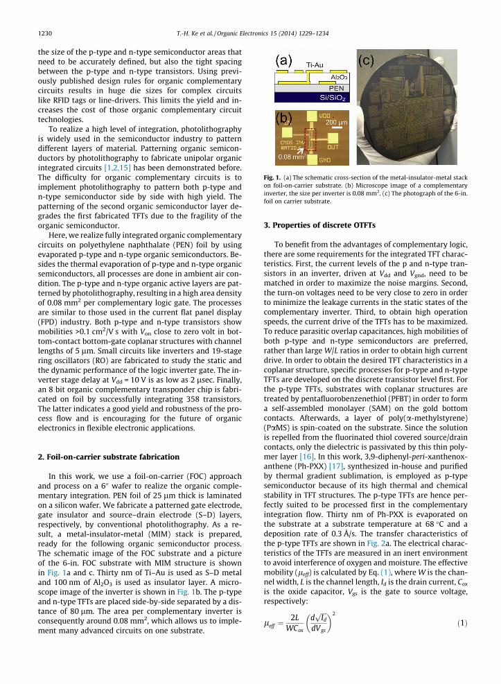
Fig. 1. (a) The schematic cross-section of the metal-insulator-metal stackon foil-on-carrier substrate. (b) Microscope image of a complementaryinverter, the size per inverter is 0.08 mm2. (c) The photograph of the 6-in.foil on carrier substrate.
1230 T.-H. Ke et al. / Organic Electronics 15 (2014) 1229–1234
the size of the p-type and n-type semiconductor areas thatneed to be accurately defined, but also the tight spacingbetween the p-type and n-type transistors. Using previ-ously published design rules for organic complementarycircuits results in huge die sizes for complex circuitslike RFID tags or line-drivers. This limits the yield and in-creases the cost of those organic complementary circuittechnologies.
To realize a high level of integration, photolithographyis widely used in the semiconductor industry to patterndifferent layers of material. Patterning organic semicon-ductors by photolithography to fabricate unipolar organicintegrated circuits [1,2,15] has been demonstrated before.The difficulty for organic complementary circuits is toimplement photolithography to pattern both p-type andn-type semiconductor side by side with high yield. Thepatterning of the second organic semiconductor layer de-grades the first fabricated TFTs due to the fragility of theorganic semiconductor.
Here, we realize fully integrated organic complementarycircuits on polyethylene naphthalate (PEN) foil by usingevaporated p-type and n-type organic semiconductors. Be-sides the thermal evaporation of p-type and n-type organicsemiconductors, all processes are done in ambient air con-dition. The p-type and n-type organic active layers are pat-terned by photolithography, resulting in a high area densityof 0.08 mm2 per complementary logic gate. The processesare similar to those used in the current flat panel display(FPD) industry. Both p-type and n-type transistors showmobilities >0.1 cm2/V s with Von close to zero volt in bot-tom-contact bottom-gate coplanar structures with channellengths of 5 lm. Small circuits like inverters and 19-stagering oscillators (RO) are fabricated to study the static andthe dynamic performance of the logic inverter gate. The in-verter stage delay at Vdd = 10 V is as low as 2 lsec. Finally,an 8 bit organic complementary transponder chip is fabri-cated on foil by successfully integrating 358 transistors.The latter indicates a good yield and robustness of the pro-cess flow and is encouraging for the future of organicelectronics in flexible electronic applications.
2. Foil-on-carrier substrate fabrication
In this work, we use a foil-on-carrier (FOC) approachand process on a 600 wafer to realize the organic comple-mentary integration. PEN foil of 25 lm thick is laminatedon a silicon wafer. We fabricate a patterned gate electrode,gate insulator and source–drain electrode (S–D) layers,respectively, by conventional photolithography. As a re-sult, a metal-insulator-metal (MIM) stack is prepared,ready for the following organic semiconductor process.The schematic image of the FOC substrate and a pictureof the 6-in. FOC substrate with MIM structure is shownin Fig. 1a and c. Thirty nm of Ti–Au is used as S–D metaland 100 nm of Al2O3 is used as insulator layer. A micro-scope image of the inverter is shown in Fig. 1b. The p-typeand n-type TFTs are placed side-by-side separated by a dis-tance of 80 lm. The area per complementary inverter isconsequently around 0.08 mm2, which allows us to imple-ment many advanced circuits on one substrate.
3. Properties of discrete OTFTs
To benefit from the advantages of complementary logic,there are some requirements for the integrated TFT charac-teristics. First, the current levels of the p and n-type tran-sistors in an inverter, driven at Vdd and Vgnd, need to bematched in order to maximize the noise margins. Second,the turn-on voltages need to be very close to zero in orderto minimize the leakage currents in the static states of thecomplementary inverter. Third, to obtain high operationspeeds, the current drive of the TFTs has to be maximized.To reduce parasitic overlap capacitances, high mobilities ofboth p-type and n-type semiconductors are preferred,rather than large W/L ratios in order to obtain high currentdrive. In order to obtain the desired TFT characteristics in acoplanar structure, specific processes for p-type and n-typeTFTs are developed on the discrete transistor level first. Forthe p-type TFTs, substrates with coplanar structures aretreated by pentafluorobenzenethiol (PFBT) in order to forma self-assembled monolayer (SAM) on the gold bottomcontacts. Afterwards, a layer of poly(a-methylstyrene)(PaMS) is spin-coated on the substrate. Since the solutionis repelled from the fluorinated thiol covered source/draincontacts, only the dielectric is passivated by this thin poly-mer layer [16]. In this work, 3,9-diphenyl-peri-xanthenox-anthene (Ph-PXX) [17], synthesized in-house and purifiedby thermal gradient sublimation, is employed as p-typesemiconductor because of its high thermal and chemicalstability in TFT structures. The p-type TFTs are hence per-fectly suited to be processed first in the complementaryintegration flow. Thirty nm of Ph-PXX is evaporated onthe substrate at a substrate temperature at 68 �C and adeposition rate of 0.3 Å/s. The transfer characteristics ofthe p-type TFTs are shown in Fig. 2a. The electrical charac-teristics of the TFTs are measured in an inert environmentto avoid interference of oxygen and moisture. The effectivemobility (leff) is calculated by Eq. (1), where W is the chan-nel width, L is the channel length, Id is the drain current, Cox
is the oxide capacitor, Vgs is the gate to source voltage,respectively:
leff ¼2L
WCox
dffiffiffiffiIdp
dVgs
� �2
ð1Þ
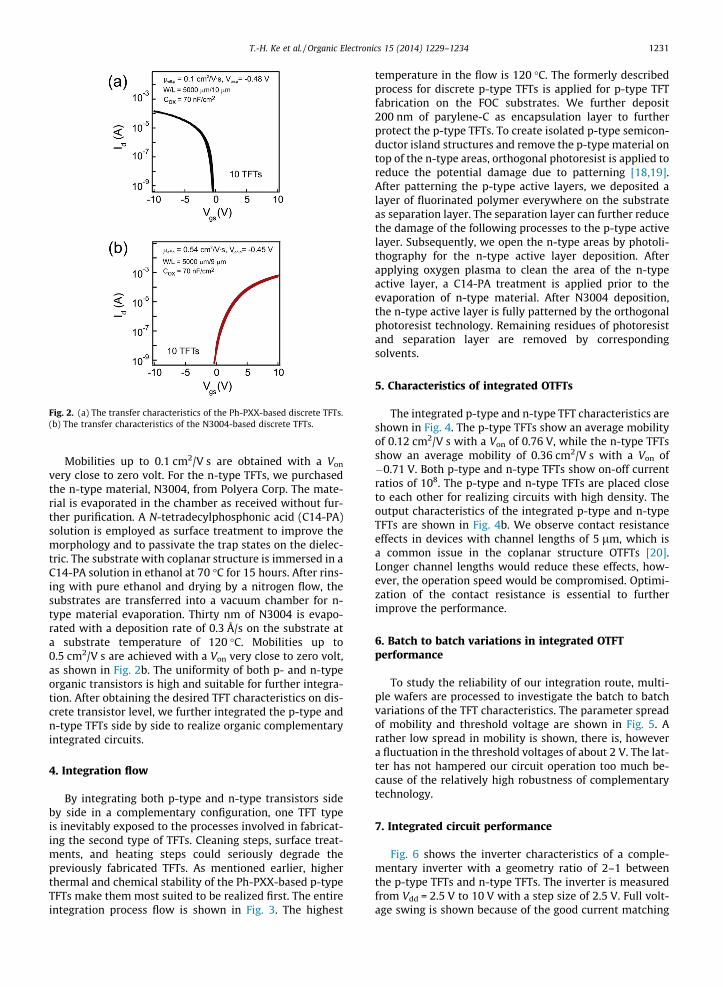
Fig. 2. (a) The transfer characteristics of the Ph-PXX-based discrete TFTs.(b) The transfer characteristics of the N3004-based discrete TFTs.
T.-H. Ke et al. / Organic Electronics 15 (2014) 1229–1234 1231
Mobilities up to 0.1 cm2/V s are obtained with a Von
very close to zero volt. For the n-type TFTs, we purchasedthe n-type material, N3004, from Polyera Corp. The mate-rial is evaporated in the chamber as received without fur-ther purification. A N-tetradecylphosphonic acid (C14-PA)solution is employed as surface treatment to improve themorphology and to passivate the trap states on the dielec-tric. The substrate with coplanar structure is immersed in aC14-PA solution in ethanol at 70 �C for 15 hours. After rins-ing with pure ethanol and drying by a nitrogen flow, thesubstrates are transferred into a vacuum chamber for n-type material evaporation. Thirty nm of N3004 is evapo-rated with a deposition rate of 0.3 Å/s on the substrate ata substrate temperature of 120 �C. Mobilities up to0.5 cm2/V s are achieved with a Von very close to zero volt,as shown in Fig. 2b. The uniformity of both p- and n-typeorganic transistors is high and suitable for further integra-tion. After obtaining the desired TFT characteristics on dis-crete transistor level, we further integrated the p-type andn-type TFTs side by side to realize organic complementaryintegrated circuits.
4. Integration flow
By integrating both p-type and n-type transistors sideby side in a complementary configuration, one TFT typeis inevitably exposed to the processes involved in fabricat-ing the second type of TFTs. Cleaning steps, surface treat-ments, and heating steps could seriously degrade thepreviously fabricated TFTs. As mentioned earlier, higherthermal and chemical stability of the Ph-PXX-based p-typeTFTs make them most suited to be realized first. The entireintegration process flow is shown in Fig. 3. The highest
temperature in the flow is 120 �C. The formerly describedprocess for discrete p-type TFTs is applied for p-type TFTfabrication on the FOC substrates. We further deposit200 nm of parylene-C as encapsulation layer to furtherprotect the p-type TFTs. To create isolated p-type semicon-ductor island structures and remove the p-type material ontop of the n-type areas, orthogonal photoresist is applied toreduce the potential damage due to patterning [18,19].After patterning the p-type active layers, we deposited alayer of fluorinated polymer everywhere on the substrateas separation layer. The separation layer can further reducethe damage of the following processes to the p-type activelayer. Subsequently, we open the n-type areas by photoli-thography for the n-type active layer deposition. Afterapplying oxygen plasma to clean the area of the n-typeactive layer, a C14-PA treatment is applied prior to theevaporation of n-type material. After N3004 deposition,the n-type active layer is fully patterned by the orthogonalphotoresist technology. Remaining residues of photoresistand separation layer are removed by correspondingsolvents.
5. Characteristics of integrated OTFTs
The integrated p-type and n-type TFT characteristics areshown in Fig. 4. The p-type TFTs show an average mobilityof 0.12 cm2/V s with a Von of 0.76 V, while the n-type TFTsshow an average mobility of 0.36 cm2/V s with a Von of�0.71 V. Both p-type and n-type TFTs show on-off currentratios of 108. The p-type and n-type TFTs are placed closeto each other for realizing circuits with high density. Theoutput characteristics of the integrated p-type and n-typeTFTs are shown in Fig. 4b. We observe contact resistanceeffects in devices with channel lengths of 5 lm, which isa common issue in the coplanar structure OTFTs [20].Longer channel lengths would reduce these effects, how-ever, the operation speed would be compromised. Optimi-zation of the contact resistance is essential to furtherimprove the performance.
6. Batch to batch variations in integrated OTFTperformance
To study the reliability of our integration route, multi-ple wafers are processed to investigate the batch to batchvariations of the TFT characteristics. The parameter spreadof mobility and threshold voltage are shown in Fig. 5. Arather low spread in mobility is shown, there is, howevera fluctuation in the threshold voltages of about 2 V. The lat-ter has not hampered our circuit operation too much be-cause of the relatively high robustness of complementarytechnology.
7. Integrated circuit performance
Fig. 6 shows the inverter characteristics of a comple-mentary inverter with a geometry ratio of 2–1 betweenthe p-type TFTs and n-type TFTs. The inverter is measuredfrom Vdd = 2.5 V to 10 V with a step size of 2.5 V. Full volt-age swing is shown because of the good current matching
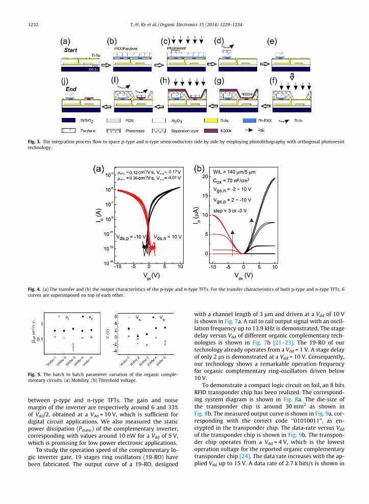
Fig. 3. The integration process flow to space p-type and n-type semiconductors side by side by employing photolithography with orthogonal photoresisttechnology.
Fig. 4. (a) The transfer and (b) the output characteristics of the p-type and n-type TFTs. For the transfer characteristics of both p-type and n-type TFTs, 6curves are superimposed on top of each other.
Fig. 5. The batch to batch parameter variation of the organic comple-mentary circuits. (a) Mobility. (b) Threshold voltage.
1232 T.-H. Ke et al. / Organic Electronics 15 (2014) 1229–1234
between p-type and n-type TFTs. The gain and noisemargin of the inverter are respectively around 6 and 33%of Vdd/2, obtained at a Vdd = 10 V, which is sufficient fordigital circuit applications. We also measured the staticpower dissipation (Pstatic) of the complementary inverter,corresponding with values around 10 nW for a Vdd of 5 V,which is promising for low power electronic applications.
To study the operation speed of the complementary lo-gic inverter gate, 19 stages ring oscillators (19-RO) havebeen fabricated. The output curve of a 19-RO, designed
with a channel length of 3 lm and driven at a Vdd of 10 Vis shown in Fig. 7a. A rail to rail output signal with an oscil-lation frequency up to 13.9 kHz is demonstrated. The stagedelay versus Vdd of different organic complementary tech-nologies is shown in Fig. 7b [21–23]. The 19-RO of ourtechnology already operates from a Vdd = 1 V. A stage delayof only 2 ls is demonstrated at a Vdd = 10 V. Consequently,our technology shows a remarkable operation frequencyfor organic complementary ring-oscillators driven below10 V.
To demonstrate a compact logic circuit on foil, an 8 bitsRFID transponder chip has been realized. The correspond-ing system diagram is shown in Fig. 8a. The die-size ofthe transponder chip is around 30 mm2 as shown inFig. 8b. The measured output curve is shown in Fig. 9a, cor-responding with the correct code ‘‘01010011’’, as en-crypted in the transponder chip. The data-rate versus Vdd
of the transponder chip is shown in Fig. 9b. The transpon-der chip operates from a Vdd = 4 V, which is the lowestoperation voltage for the reported organic complementarytransponder chip [24]. The data rate increases with the ap-plied Vdd up to 15 V. A data rate of 2.7 k bits/s is shown in
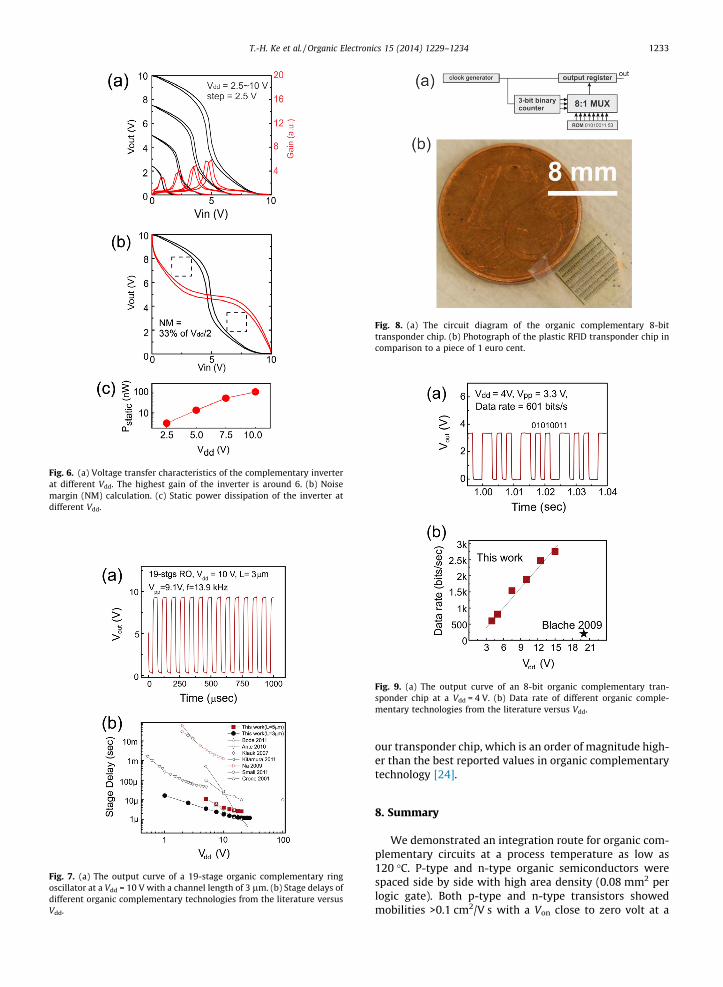
Fig. 6. (a) Voltage transfer characteristics of the complementary inverterat different Vdd. The highest gain of the inverter is around 6. (b) Noisemargin (NM) calculation. (c) Static power dissipation of the inverter atdifferent Vdd.
Fig. 7. (a) The output curve of a 19-stage organic complementary ringoscillator at a Vdd = 10 V with a channel length of 3 lm. (b) Stage delays ofdifferent organic complementary technologies from the literature versusVdd.
Fig. 8. (a) The circuit diagram of the organic complementary 8-bittransponder chip. (b) Photograph of the plastic RFID transponder chip incomparison to a piece of 1 euro cent.
Fig. 9. (a) The output curve of an 8-bit organic complementary tran-sponder chip at a Vdd = 4 V. (b) Data rate of different organic comple-mentary technologies from the literature versus Vdd.
T.-H. Ke et al. / Organic Electronics 15 (2014) 1229–1234 1233
our transponder chip, which is an order of magnitude high-er than the best reported values in organic complementarytechnology [24].
8. Summary
We demonstrated an integration route for organic com-plementary circuits at a process temperature as low as120 �C. P-type and n-type organic semiconductors werespaced side by side with high area density (0.08 mm2 perlogic gate). Both p-type and n-type transistors showedmobilities >0.1 cm2/V s with a Von close to zero volt at a
1234 T.-H. Ke et al. / Organic Electronics 15 (2014) 1229–1234
channel length of 5 lm in a coplanar structure. Elementarybuilding blocks for digital logic from inverters to 19 stagering oscillators were fabricated to study the static and dy-namic performance of the logic inverter gate. A 2 lsecstage delay of organic complementary circuits at a drivingvoltage (Vdd) = 10 V was demonstrated. To further studythe integration level, an 8 bit transponder chip was fabri-cated. 358 transistors were successfully integrated torealize the organic complementary 8 bit transponderchip, which indicate the promising future for organicelectronics.
Acknowledgements
The authors would like to acknowledge financial sup-port through the EU project COSMIC (FP7 ICT-247681)and ONE-P (FP7-NMP-212311). This work was performedin a collaboration between IMEC and TNO in the frame ofthe HOLST Centre. The authors want to thank Polyera Corp.for supplying n-type semiconductor materials. The authorsalso want to thank Dr. Barry Rand for Ph-PXX purification.
References
[1] K. Myny, E. Van Veenendaal, G.H. Gelinck, J. Genoe, W. Dehaene, P.Heremans, Microprocessor on plastic foil, IEEE J. Solid State Circ. 47(2012) 284–291.
[2] K. Myny, M.J. Beenhakkers, N.A.J.M. Van Aerle, G.H. Gelinck, J. Genoe,W. Dehaene, et al., Unipolar organic transistor circuits made robustby dual-gate technology, IEEE J. Solid State Circ. 46 (2011) 1223–1230.
[3] H. Klauk, U. Zschieschang, J. Pflaum, M. Halik, Ultralow-powerorganic complementary circuits, Nature 445 (2007) 745–748.
[4] M. Kitamura, Y. Kuzumoto, S. Aomori, Y. Arakawa, High-frequencyorganic complementary ring oscillator operating up to 200 kHz,Appl. Phys. Express 4 (2011) 051601.
[5] B. Crone, A. Dodabalapur, Y. Lin, R. Filas, Z. Bao, A. LaDuca, et al.,Large-scale complementary integrated circuits based on organictransistors, Nature 403 (2000) 521–523.
[6] K. Ishida, N. Masunaga, Z. Zhou, T. Yasufuku, T. Sekitani, U.Zschieschang, et al., A stretchable EMI measurement sheet with8 � 8 coil array, 2V organic CMOS decoder, and �70dBm EMIdetection circuits in 0.18 lm CMOS, Isscc Dig. Tech. Pap. (2009)472–474.
[7] K. Ishida, T. Huang, K. Honda, T. Sekitani, H. Nakajima, H. Maeda,et al., 100V AC power meter system-on-a-film (SoF) integrating 20Vorganic CMOS digital and analog circuits with floating gate for
process-variation compensation and 100V organic PMOS rectifier,Isscc Dig. Tech. Pap. 326 (2011) 136–137.
[8] B. Yoo, B.A. Jones, D. Basu, D. Fine, T. Jung, S. Mohapatra, et al., High-performance solution-deposited n-channel organic transistors andtheir complementary circuits, Adv. Mater. 19 (2007) 4028–4032.
[9] H. Yan, Y. Zheng, R. Blache, C. Newman, S. Lu, J. Woerle, et al.,Solution Processed top-gate n-channel transistors andcomplementary circuits on plastics operating in ambientconditions, Adv. Mater. 20 (2008) 3393–3398.
[10] T.N. Ng, S. Sambandan, R. Lujan, A.C. Arias, C.R. Newman, H. Yan,et al., Electrical stability of inkjet-patterned organic complementaryinverters measured in ambient conditions, Appl. Phys. Lett. 94(2009) 233307.
[11] T.N. Ng, D.E. Schwartz, L.L. Lavery, G.L. Whiting, B. Russo, B. Krusor,et al., Sci. Rep. 2 (2012) 585.
[12] W. Smaal, C. Kjellander, Y. Jeong, A. Tripathi, B. Van Der Putten, A.Facchetti, et al., Complementary integrated circuits on plastic foilusing inkjet printed n- and p-type organic semiconductors:fabrication, characterization, and circuit analysis, Org. Electron. 13(2012) 1686–1692.
[13] D.E. Schwartz, T.N. Ng, Printed organic shift registers, IEEE ElectronDevice Lett. 34 (2013) 271–273.
[14] S.H. Kim, S.H. Lee, Y.G. Kim, J. Jang, Ink-jet-printed organic thin-filmtransistors for low-voltage-driven CMOS circuits with solution-processed AlO X gate insulator, IEEE Electron Device Lett. 34 (2013)2012–2014.
[15] K. Myny, S. Steudel, S. Smout, P. Vicca, F. Furthner, B. van der Putten,et al., Organic RFID transponder chip with data rate compatible withelectronic product coding, Org. Electron. 11 (2010) 1176–1179.
[16] K. Myny, S. De Vusser, S. Steudel, D. Janssen, R. Müller, S. De Jonge,et al., Self-aligned surface treatment for thin-film organic transistors,Appl. Phys. Lett. 88 (2006) 222103.
[17] N. Kobayashi, M. Sasaki, K. Nomoto, Stable peri-xanthenoxanthenethin-film transistors with efficient carrier injection, Chem. Mater. 21(2009) 552–556.
[18] S. Steudel, K. Myny, S. De Vusser, J. Genoe, P. Heremans, Patterning oforganic thin film transistors by oxygen plasma etch, Appl. Phys. Lett.89 (2006) 183503.
[19] A.A. Zakhidov, J.-K. Lee, J.A. DeFranco, H.H. Fong, P.G. Taylor, M.Chatzichristidi, et al., Orthogonal processing: a new strategy fororganic electronics, Chem. Sci. 2 (2011) 1178–1182.
[20] H. Klauk, Organic thin-film transistors, Chem. Soc. Rev. 39 (2010)2643–2666.
[21] J.H. Na, M. Kitamura, Y. Arakawa, Low-voltage-operating organiccomplementary circuits based on pentacene and C60 transistors,Thin Solid Films 517 (2009) 2079–2082.
[22] F. Ante, F. Letzkus, J. Butschke, U. Zschieschang, J.N. Burghartz, K.Kern, et al., Top-contact organic transistors and complementarycircuits fabricated using high-resolution silicon stencil masks, in:68th Device Res. Conf., 2010, pp. 175–176.
[23] D. Bode, K. Myny, B. Verreet, B. van der Putten, P. Bakalov, S. Steudel,et al., Organic complementary oscillators with stage-delays below1ls, Appl. Phys. Lett. 96 (2010) 133307.
[24] B. Robert, J. Krumm, W. Fix, Organic CMOS circuits for RFIDapplications, Isscc Dig. Tech. Pap. 50 (2009) 208–210.