Embed Size (px)
Citation preview
Computer Science and Artificial Intelligence Laboratory
Technical Report
m a s s a c h u s e t t s i n s t i t u t e o f t e c h n o l o g y, c a m b r i d g e , m a 0 213 9 u s a — w w w. c s a i l . m i t . e d u
MIT-CSAIL-TR-2007-003 January 11, 2007
Scale Control Processor Test-ChipChrstopher Batten, Ronny Krashinsky and
Krste Asanovic �
Scale Control Processor Test-Chip
Christopher Batten, Ronny Krashinsky, and Krste Asanovic
Massachusetts Institute of TechnologyComputer Science and Artificial Intelligence Laboratory
32 Vassar Street, 32-G736Cambridge, MA 02139
January 5, 2007
We are investigating vector-thread architectures which provide competitive performanceand e!ciency across a broad class of application domains [1, 4]. Vector-thread architecturesunify data-level, thread-level, and instruction-level parallelism, providing new ways of par-allelizing codes that are di!cult to vectorize or that incur excessive synchronization costswhen multithreaded. To illustrate these ideas we have developed the Scale processor, whichis an example of a vector-thread architecture designed for low-power and high-performanceembedded systems. The prototype includes a single-issue 32-bit RISC control processor, avector-thread unit which supports up to 128 virtual processor threads and can execute upto 16 instructions per cycle, and a 32KB shared primary cache.
Since the Scale vector-thread processor is a large and complex design (especially for anacademic project), we first designed and fabricated the Scale Test Chip (STC1). STC1includes a simplified version of the Scale control processor, 8KB of RAM, a host interface,and a custom clock generator. STC1 helped mitigate the risk involved in fabricating the fullScale chip in several ways. First, we were able to establish and test our CAD toolflow. Ourtoolflow included several custom tools which had not previously been used in any tapeouts.Second, we were able to better characterize our target package and process. For example,STC1 enabled us to better correlate the static timing numbers from our CAD tools withactual silicon and also to characterize the expected rise/fall times of our external signalpins. Finally, STC1 allowed us to test our custom clock generator. We used our experienceswith STC1 to help us implement the Scale vector-thread processor. Scale was taped out onOctober 15, 2006 and it is currently being fabricated through MOSIS. This report discussesthe fabrication of STC1 and presents power and performance results.
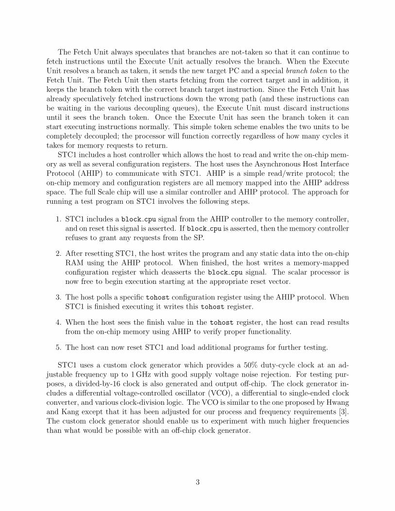
1 Overview
Figure 1 shows a high-level block diagram of STC1. The scalar processor (SP) is a singleissue in-order processor which implements a subset of the MIPS-II ISA. The SP is fullyinterlocked and does not include programmer-visible branch delay slots or load-use delayslots. To interface with the memory system, the SP is divided into two decoupled units: theFetch Unit and the Execute Unit. The Fetch Unit is responsible for generating instructionaddresses and then issuing instruction fetch requests to the memory system. The ExecuteUnit is responsible for executing the instructions. For load and store instructions, the ExecuteUnit handles issuing the appropriate memory request and then writing back load data whenit returns.
In the full Scale processor many requesters arbitrate for a single shared cache. The cacheinterface is fully decoupled: a requester issues a memory request and then some numberof cycles later a memory response is returned to the requester. Therefore, in STC1 thedecoupled Fetch and Execute Units are designed to continue operating even if one of theunits is blocked from making a request. For example, if the Fetch Unit cannot issue aninstruction fetch due to a conflict with another requester, the Execute Unit can continue toexecute arithmetic instructions and even issue new load or store requests. Similarly, if theExecute Unit is blocked from issuing a memory request, the Fetch Unit can continue to runahead and fetch additional instructions. In STC1, there are only three requesters and theserequesters directly access a single bank of on-chip memory instead of accessing the Scalecache. The STC1 memory controller uses a fixed priority scheme to arbitrate between thesethree requesters.
The Fetch Unit consists of a single pipeline stage, while the Execute Unit consists offour pipeline stages: decode, execute, memory, and writeback. Note that the SP makes useof a two write port register file so that arithmetic instructions write the register file in theexecute stage while load instructions write the register file in the writeback stage. The SPmanages instruction dependencies to bypass or stall as needed.
Fetch Exec
AHIPController
AHIP Data (8b)
AHIP Control (2b)
Clock Out
VCO Control Scalar Processor
RAMSubbank
(2KB)
RAMSubbank
(2KB)
RAMSubbank
(2KB)
RAMSubbank
(2KB)
Clock Gen
MC
WX
RX
Figure 1: Scale Test-Chip (STC1) Block Dia-gram. Address buses are shown with dashedlines, while data buses are shown with solidlines. STC1 includes a scalar processor (SP),four 2 KB RAM subbanks, memory controller(MC), read crossbar (RX), write crossbar(WX), Asynchronous Host Interface Protocol(AHIP) controller, and a custom clock gener-ator block. The SP is in turn composed of twodecoupled units: a Fetch Unit responsible forfetching instructions from the on-chip RAM,and an Execute Unit responsible for actuallyexecuting the instructions.
2
The Fetch Unit always speculates that branches are not-taken so that it can continue tofetch instructions until the Execute Unit actually resolves the branch. When the ExecuteUnit resolves a branch as taken, it sends the new target PC and a special branch token to theFetch Unit. The Fetch Unit then starts fetching from the correct target and in addition, itkeeps the branch token with the correct branch target instruction. Since the Fetch Unit hasalready speculatively fetched instructions down the wrong path (and these instructions canbe waiting in the various decoupling queues), the Execute Unit must discard instructionsuntil it sees the branch token. Once the Execute Unit has seen the branch token it canstart executing instructions normally. This simple token scheme enables the two units to becompletely decoupled; the processor will function correctly regardless of how many cycles ittakes for memory requests to return.
STC1 includes a host controller which allows the host to read and write the on-chip mem-ory as well as several configuration registers. The host uses the Asynchronous Host InterfaceProtocol (AHIP) to communicate with STC1. AHIP is a simple read/write protocol; theon-chip memory and configuration registers are all memory mapped into the AHIP addressspace. The full Scale chip will use a similar controller and AHIP protocol. The approach forrunning a test program on STC1 involves the following steps.
1. STC1 includes a block cpu signal from the AHIP controller to the memory controller,and on reset this signal is asserted. If block cpu is asserted, then the memory controllerrefuses to grant any requests from the SP.
2. After resetting STC1, the host writes the program and any static data into the on-chipRAM using the AHIP protocol. When finished, the host writes a memory-mappedconfiguration register which deasserts the block cpu signal. The scalar processor isnow free to begin execution starting at the appropriate reset vector.
3. The host polls a specific tohost configuration register using the AHIP protocol. WhenSTC1 is finished executing it writes this tohost register.
4. When the host sees the finish value in the tohost register, the host can read resultsfrom the on-chip memory using AHIP to verify proper functionality.
5. The host can now reset STC1 and load additional programs for further testing.
STC1 uses a custom clock generator which provides a 50% duty-cycle clock at an ad-justable frequency up to 1GHz with good supply voltage noise rejection. For testing pur-poses, a divided-by-16 clock is also generated and output o"-chip. The clock generator in-cludes a di"erential voltage-controlled oscillator (VCO), a di"erential to single-ended clockconverter, and various clock-division logic. The VCO is similar to the one proposed by Hwangand Kang except that it has been adjusted for our process and frequency requirements [3].The custom clock generator should enable us to experiment with much higher frequenciesthan what would be possible with an o"-chip clock generator.
3
2 Implementation and Verification
A C++ functional model served as the reference implementation for STC1. This functionalmodel is linked with a C++ test harness to enable loading test programs, running the tests,and reading the results. After implementing the STC1 RTL in Verilog, we used TenisonVTOC to translate the Verilog into C++. We were then able to link the RTL modelwith the same C++ test harness used for the functional model. We verified correctnessby comparing the results from running the same tests on both the functional and RTLmodels. In addition to a suite of custom directed tests, we developed Torture, a random testprogram generator. The challenge in generating random tests is to create legal programs thatrun correctly and also stress di"erent corner cases in the design. Torture randomly generatesrelatively simple instruction sequences of various types, and then randomly interleaves thesesequences to construct complex yet correct programs. By tuning parameters which controlthe breakdown of instruction sequence types, we can stress di"erent aspects of STC1.
Much of STC1 was implemented using standard cells and SRAM blocks provided byArtisan. To achieve a high-performance and e!cient processor, we made extensive use offine-grain standard-cell pre-placement. We wrote several custom tools and gate-level buildersto pre-place individual standard cells into datapath bitslices and register file arrays. Thecontrol logic was synthesized using Synopsys DesignCompiler and placed & routed usingCadence Encounter. After integrating pre-placed blocks with automatically synthesized andplaced & routed blocks, the final gate-level Verilog RTL was formally verified against thereference Verilog RTL using Synopsys Formality.
To verify the final GDSII layout for the chip, we ran DRC and LVS using Mentor Calibre.A final check of correct functionality was provided by running tests on the extracted Spicenetlist using Synopsys Nanosim. VCD signal traces generated by the reference RTL modelwere used to drive the input pins of the chip and verify the output pins.
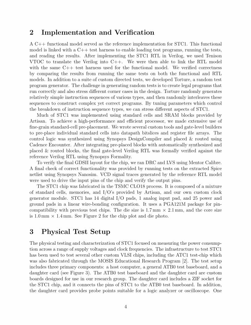
The STC1 chip was fabricated in the TSMC CLO18 process. It is composed of a mixtureof standard cells, memories, and I/O’s provided by Artisan, and our own custom clockgenerator module. STC1 has 14 digital I/O pads, 1 analog input pad, and 25 power andground pads in a linear wire-bonding configuration. It uses a PGA121M package for pin-compatibility with previous test chips. The die size is 1.7mm ! 2.1mm, and the core sizeis 1.0 mm ! 1.4mm. See Figure 2 for the chip plot and die photo.
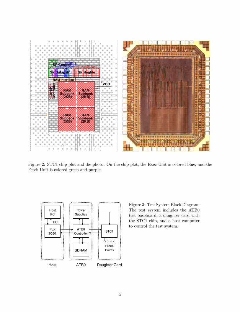
3 Physical Test Setup
The physical testing and characterization of STC1 focused on measuring the power consump-tion across a range of supply voltages and clock frequencies. The infrastructure to test STC1has been used to test several other custom VLSI chips, including the ATC1 test-chip whichwas also fabricated through the MOSIS Educational Research Program [2]. The test setupincludes three primary components: a host computer, a general ATB0 test baseboard, and adaughter card (see Figure 3). The ATB0 test baseboard and the daughter card are customboards designed for use in our research group. The daughter card includes a ZIF socket forthe STC1 chip, and it connects the pins of STC1 to the ATB0 test baseboard. In addition,the daughter card provides probe points suitable for a logic analyzer or oscilloscope. One
4
SP Datapath SP Regfile
RAMSubbank
(2KB)
RAMSubbank
(2KB)
RAMSubbank
(2KB)
RAMSubbank
(2KB)
AH
IPC
on
tro
ller
SP Control
RAM Interface
VCO
Figure 2: STC1 chip plot and die photo. On the chip plot, the Exec Unit is colored blue, and theFetch Unit is colored green and purple.
HostPC
PLX9050
ATB0Controller
PowerSupplies
ProbePoints
PCI
SDRAM
STC1
Host ATB0 Daughter Card
Figure 3: Test System Block Diagram.The test system includes the ATB0test baseboard, a daughter card withthe STC1 chip, and a host computerto control the test system.
5
of these probe points is connected to the clock output of STC1 enabling us to measure theperformance of the custom on-chip clock generator.
The ATB0 test baseboard includes an ATB0 controller, 96MB of SDRAM, and severaladjustable power supplies with current measurement. The ATB0 controller is implementedin a Xilinx FPGA and it is able to communicate directly with STC1 using the AHIP protocol.Additionally, the ATB0 controller can adjust the voltage of the STC1 power supplies andthe analog input of the voltage-controlled oscillator on STC1. The ATB0 controller is alsoable to read the current being drawn by each power supply. Using this system, we were ableto accurately measure the power consumption of STC1 for various voltages and frequencies.
Software on the host PC communicates with the ATB0 controller using a PLX 9050 PCIcard. A command protocol allows the software to adjust the power supplies, read data fromthe SDRAM, and communicate with STC1. More information about our test setup can befound online at http://www.cag.csail.mit.edu/scale/hardware.
4 Results
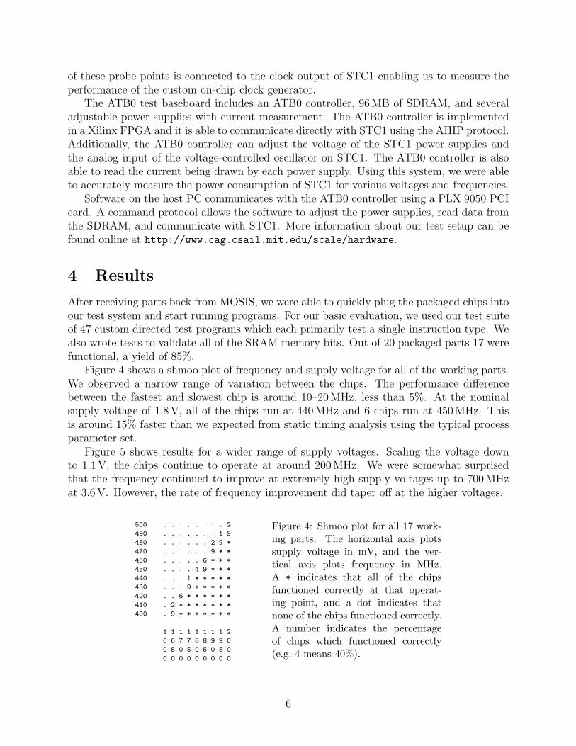
After receiving parts back from MOSIS, we were able to quickly plug the packaged chips intoour test system and start running programs. For our basic evaluation, we used our test suiteof 47 custom directed test programs which each primarily test a single instruction type. Wealso wrote tests to validate all of the SRAM memory bits. Out of 20 packaged parts 17 werefunctional, a yield of 85%.
Figure 4 shows a shmoo plot of frequency and supply voltage for all of the working parts.We observed a narrow range of variation between the chips. The performance di"erencebetween the fastest and slowest chip is around 10–20 MHz, less than 5%. At the nominalsupply voltage of 1.8V, all of the chips run at 440MHz and 6 chips run at 450MHz. Thisis around 15% faster than we expected from static timing analysis using the typical processparameter set.
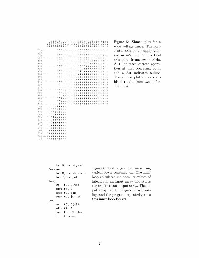
Figure 5 shows results for a wider range of supply voltages. Scaling the voltage downto 1.1V, the chips continue to operate at around 200MHz. We were somewhat surprisedthat the frequency continued to improve at extremely high supply voltages up to 700MHzat 3.6V. However, the rate of frequency improvement did taper o" at the higher voltages.
500 . . . . . . . . 2490 . . . . . . . 1 9480 . . . . . . 2 9 *470 . . . . . . 9 * *460 . . . . . 6 * * *450 . . . . 4 9 * * *440 . . . 1 * * * * *430 . . . 9 * * * * *420 . . 6 * * * * * *410 . 2 * * * * * * *400 . 9 * * * * * * *
1 1 1 1 1 1 1 1 26 6 7 7 8 8 9 9 00 5 0 5 0 5 0 5 00 0 0 0 0 0 0 0 0
Figure 4: Shmoo plot for all 17 work-ing parts. The horizontal axis plotssupply voltage in mV, and the ver-tical axis plots frequency in MHz.A * indicates that all of the chipsfunctioned correctly at that operat-ing point, and a dot indicates thatnone of the chips functioned correctly.A number indicates the percentageof chips which functioned correctly(e.g. 4 means 40%).
6
1 1 1 1 1 1 1 1 1 2 2 2 2 2 2 2 2 2 2 3 3 3 3 3 3 3 3 3 3 41 2 3 4 5 6 7 8 9 0 1 2 3 4 5 6 7 8 9 0 1 2 3 4 5 6 7 8 9 00 0 0 0 0 0 0 0 0 0 0 0 0 0 0 0 0 0 0 0 0 0 0 0 0 0 0 0 0 00 0 0 0 0 0 0 0 0 0 0 0 0 0 0 0 0 0 0 0 0 0 0 0 0 0 0 0 0 0
750 ------------- . . . . . . . . . . . . . . . . . . . . . . . . .740 . . . . . . . . . . . . . . . . . . . . . . . . .730 . . . . . . . . . . . . . . . . . . . . . . . . .720 . . . . . . . . . . . . . . . . . . . . . . . . .710 . . . . . . . . . . . . . . . . . . . . . . * * .700 ------------- . . . . . . . . . . . . . . . . . . . . * * * * .690 . . . . . . . . . . . . . . . . . . . * * * * * .680 . . . . . . . . . . . . . . . . . * * * * * * . .670 . . . . . . . . . . . . . . . . * * * * * * * . .660 . . . . . . . . . . . . . . . . * * * * * * * . .650 ------------- . . . . . . . . . . . . . . * * * * * * * * * * .640 . . . . . . . . . . . . . . * * * * * * * * * * .630 . . . . . . . . . . . . . * * * * * * * * * * . .620 . . . . . . . . . . . . * * * * * * * * * * * * .610 . . . . . . . . . . . * . * * * * * * * * * * . .600 ------------- . . . . . . . . . . . * * * * * * * * * * * * . .590 . . . . . . . . . . * * * * * * * * * * * * * * .580 . . . . . . . . . . * * * * * * * * * * * * * . .570 . . . . . . . . . * * * * * * * * * * * * * * * *560 . . . . . . . . . * * * * * * * * * * * * * * * *550 ------------- . . . . . . . * * * * * * * * * * * * * * * * * .540 . . . . . . . * * * * * * * * * * * * * * * * . *530 . . . . . . . * * * * * * * * * * * * * * * * * *520 . . . . . . * * * * * * * * * * * * * * * * * * *510 . . . . . . * * * * * * * * * * * * * * * * * * *500 ------------- . . . . . * * * * * * * * * * * * * * * * * * * *490 . . . . * * * * * * * * * * * * * * * * * * * * *480 . . . . * * * * * * * * * * * * * * * * * * * * *470 . . . * * * * * * * * * * * * * * * * * * * * * *460 . . . * * * * * * * * * * * * * * * * * . * * * *450 ------------- . . . * * * * * * * * * * * * * * * * * * * * * *440 . . * * * * * * * * * * * * * * * * * * * * * * *430 . . * * * * * * * * * * * * * * * * * * * * * * *420 . . * * * * * * * * * * * * * * * * * * * * * * *410 . * * * * * * * * * * * * * * * * * * * * * * * *400 ------------- . * * * * * * * * * * * * * * * * * * * * * * * *390 . . . . . * * * * *380 . . . . . * * * * *370 . . . . . * * * * *360 . . . . . * * * * *350 --- . . . . * * * * * *340 . . . . * * * * * *330 . . . . * * * * * *320 . . . * * * * * * *310 . . . * * * * * * *300 --- . . . * * * * * * *290 . . . * * * * * * *280 . . * * * * * * * *270 . . * * * * * * * *260 . . * * * * * * * *250 --- . . * * * * * * * *240 . * * * * * * * * *230 . * * * * * * * * *220 . * * * * * * * * *210 . * * * * * * * * *200 --- * * * * * * * * * *190 * * * * * * * * * *180 * * * * * * * * * *
Figure 5: Shmoo plot for awide voltage range. The hori-zontal axis plots supply volt-age in mV, and the verticalaxis plots frequency in MHz.A * indicates correct opera-tion at that operating pointand a dot indicates failure.The shmoo plot shows com-bined results from two di!er-ent chips.
la t9, input_endforever:
la t8, input_startla t7, output
loop:lw t0, 0(t8)addu t8, 4bgez t0, possubu t0, $0, t0
pos:sw t0, 0(t7)addu t7, 4bne t8, t9, loopb forever
Figure 6: Test program for measuringtypical power consumption. The innerloop calculates the absolute values ofintegers in an input array and storesthe results to an output array. The in-put array had 10 integers during test-ing, and the program repeatedly runsthis inner loop forever.
7
STC1 power at 100 MHz
0
20
40
60
80
100
120
140
160
180
200
220
240
260
1.0 1.2 1.4 1.6 1.8 2.0 2.2 2.4 2.6 2.8 3.0 3.2 3.4 3.6 3.8 4.0
VDD (V)
po
we
r (m
W)
abs loop power
nops power
idle power
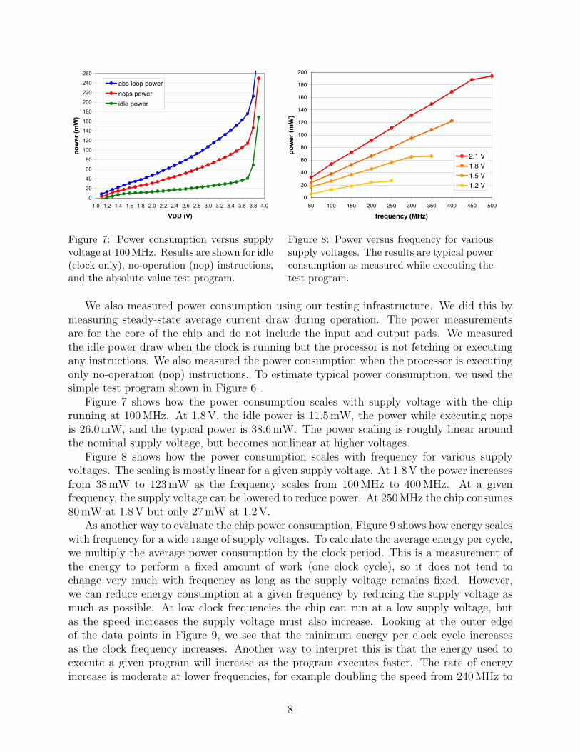
Figure 7: Power consumption versus supplyvoltage at 100MHz. Results are shown for idle(clock only), no-operation (nop) instructions,and the absolute-value test program.
0
20
40
60
80
100
120
140
160
180
200
50 100 150 200 250 300 350 400 450 500
frequency (MHz)
pow
er (m
W)
2.1 V1.8 V1.5 V1.2 V
Figure 8: Power versus frequency for varioussupply voltages. The results are typical powerconsumption as measured while executing thetest program.
We also measured power consumption using our testing infrastructure. We did this bymeasuring steady-state average current draw during operation. The power measurementsare for the core of the chip and do not include the input and output pads. We measuredthe idle power draw when the clock is running but the processor is not fetching or executingany instructions. We also measured the power consumption when the processor is executingonly no-operation (nop) instructions. To estimate typical power consumption, we used thesimple test program shown in Figure 6.
Figure 7 shows how the power consumption scales with supply voltage with the chiprunning at 100 MHz. At 1.8V, the idle power is 11.5 mW, the power while executing nopsis 26.0mW, and the typical power is 38.6mW. The power scaling is roughly linear aroundthe nominal supply voltage, but becomes nonlinear at higher voltages.
Figure 8 shows how the power consumption scales with frequency for various supplyvoltages. The scaling is mostly linear for a given supply voltage. At 1.8V the power increasesfrom 38mW to 123 mW as the frequency scales from 100MHz to 400MHz. At a givenfrequency, the supply voltage can be lowered to reduce power. At 250MHz the chip consumes80mW at 1.8V but only 27mW at 1.2V.
As another way to evaluate the chip power consumption, Figure 9 shows how energy scaleswith frequency for a wide range of supply voltages. To calculate the average energy per cycle,we multiply the average power consumption by the clock period. This is a measurement ofthe energy to perform a fixed amount of work (one clock cycle), so it does not tend tochange very much with frequency as long as the supply voltage remains fixed. However,we can reduce energy consumption at a given frequency by reducing the supply voltage asmuch as possible. At low clock frequencies the chip can run at a low supply voltage, butas the speed increases the supply voltage must also increase. Looking at the outer edgeof the data points in Figure 9, we see that the minimum energy per clock cycle increasesas the clock frequency increases. Another way to interpret this is that the energy used toexecute a given program will increase as the program executes faster. The rate of energyincrease is moderate at lower frequencies, for example doubling the speed from 240MHz to
8
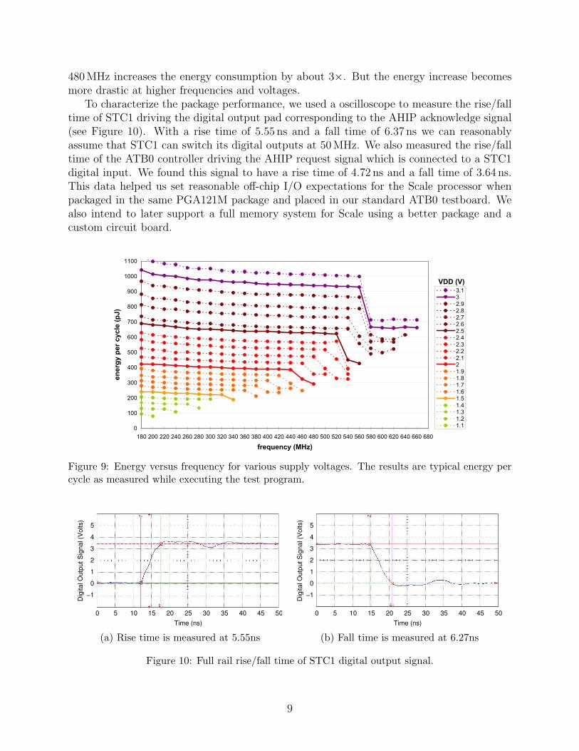
480MHz increases the energy consumption by about 3!. But the energy increase becomesmore drastic at higher frequencies and voltages.
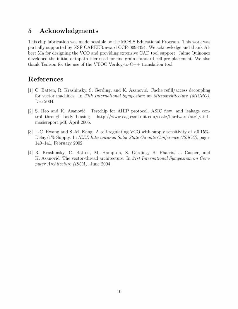
To characterize the package performance, we used a oscilloscope to measure the rise/falltime of STC1 driving the digital output pad corresponding to the AHIP acknowledge signal(see Figure 10). With a rise time of 5.55 ns and a fall time of 6.37 ns we can reasonablyassume that STC1 can switch its digital outputs at 50MHz. We also measured the rise/falltime of the ATB0 controller driving the AHIP request signal which is connected to a STC1digital input. We found this signal to have a rise time of 4.72 ns and a fall time of 3.64 ns.This data helped us set reasonable o"-chip I/O expectations for the Scale processor whenpackaged in the same PGA121M package and placed in our standard ATB0 testboard. Wealso intend to later support a full memory system for Scale using a better package and acustom circuit board.
0
100
200
300
400
500
600
700
800
900
1000
1100
180 200 220 240 260 280 300 320 340 360 380 400 420 440 460 480 500 520 540 560 580 600 620 640 660 680
frequency (MHz)
en
erg
y p
er
cy
cle
(p
J)
3.1
3
2.9
2.8
2.7
2.6
2.5
2.4
2.3
2.2
2.1
2
1.9
1.8
1.7
1.6
1.5
1.4
1.3
1.2
1.1
VDD (V)
Figure 9: Energy versus frequency for various supply voltages. The results are typical energy percycle as measured while executing the test program.
5 10 15 20 25 30 35 40 45 500
Dig
ital O
utpu
t Sig
nal (
Vol
ts)
2
5
4
3
1
0
!1
Time (ns)
(a) Rise time is measured at 5.55ns
0 5 10 15 20 25 30 35 40 45 50
5
4
3
2
1
0
!1Dig
ital O
utpu
t Sig
nal (
Vol
ts)
Time (ns)
(b) Fall time is measured at 6.27ns
Figure 10: Full rail rise/fall time of STC1 digital output signal.
9
5 Acknowledgments
This chip fabrication was made possible by the MOSIS Educational Program. This work waspartially supported by NSF CAREER award CCR-0093354. We acknowledge and thank Al-bert Ma for designing the VCO and providing extensive CAD tool support. Jaime Quinonezdeveloped the initial datapath tiler used for fine-grain standard-cell pre-placement. We alsothank Tenison for the use of the VTOC Verilog-to-C++ translation tool.
References
[1] C. Batten, R. Krashinsky, S. Gerding, and K. Asanovic. Cache refill/access decouplingfor vector machines. In 37th International Symposium on Microarchitecture (MICRO),Dec 2004.
[2] S. Heo and K. Asanovic. Testchip for AHIP protocol, ASIC flow, and leakage con-trol through body biasing. http://www.cag.csail.mit.edu/scale/hardware/atc1/atc1-mosisreport.pdf, April 2005.
[3] I.-C. Hwang and S.-M. Kang. A self-regulating VCO with supply sensitivity of <0.15%-Delay/1%-Supply. In IEEE International Solid-State Circuits Conference (ISSCC), pages140–141, February 2002.
[4] R. Krashinsky, C. Batten, M. Hampton, S. Gerding, B. Pharris, J. Casper, andK. Asanovic. The vector-thread architecture. In 31st International Symposium on Com-puter Architecture (ISCA), June 2004.
10