Embed Size (px)
Citation preview

Scalable Many-Core Memory Systems Lecture 2, Topic 1: DRAM Basics and
DRAM Scaling
Prof. Onur Mutlu http://www.ece.cmu.edu/~omutlu
[email protected] HiPEAC ACACES Summer School 2013
July 16, 2013
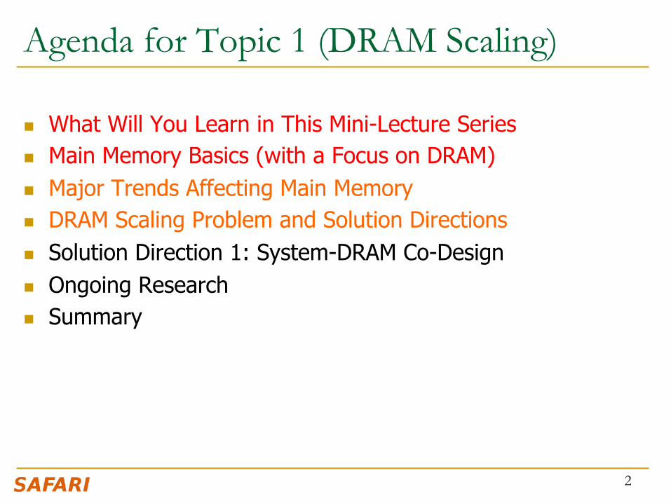
Agenda for Topic 1 (DRAM Scaling)
n What Will You Learn in This Mini-Lecture Series n Main Memory Basics (with a Focus on DRAM) n Major Trends Affecting Main Memory n DRAM Scaling Problem and Solution Directions n Solution Direction 1: System-DRAM Co-Design n Ongoing Research n Summary
2
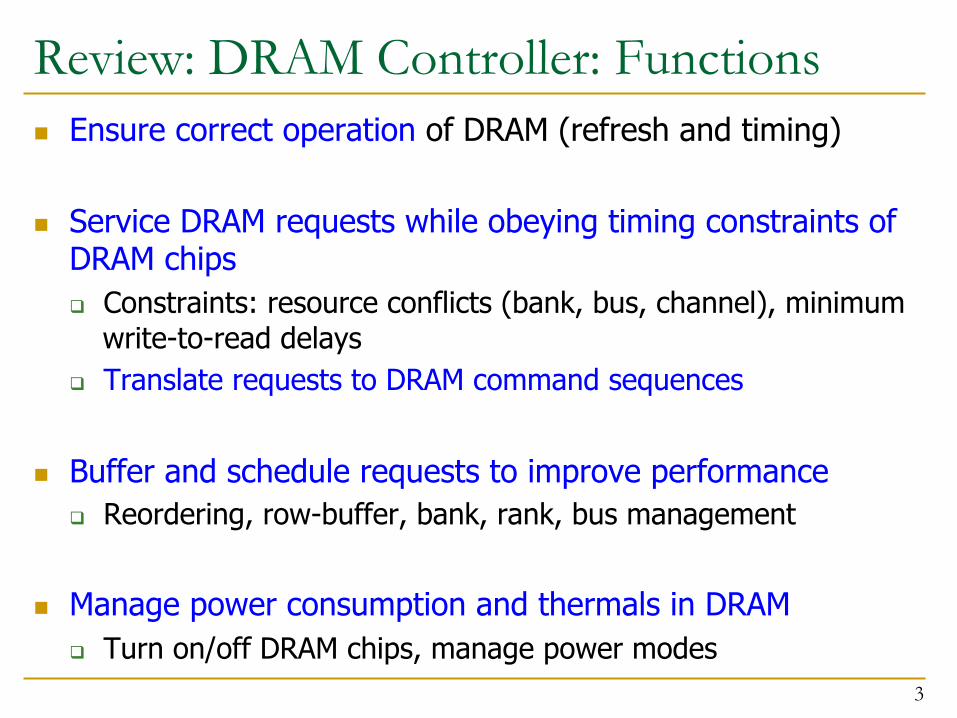
Review: DRAM Controller: Functions n Ensure correct operation of DRAM (refresh and timing)
n Service DRAM requests while obeying timing constraints of DRAM chips q Constraints: resource conflicts (bank, bus, channel), minimum
write-to-read delays q Translate requests to DRAM command sequences
n Buffer and schedule requests to improve performance q Reordering, row-buffer, bank, rank, bus management
n Manage power consumption and thermals in DRAM q Turn on/off DRAM chips, manage power modes
3
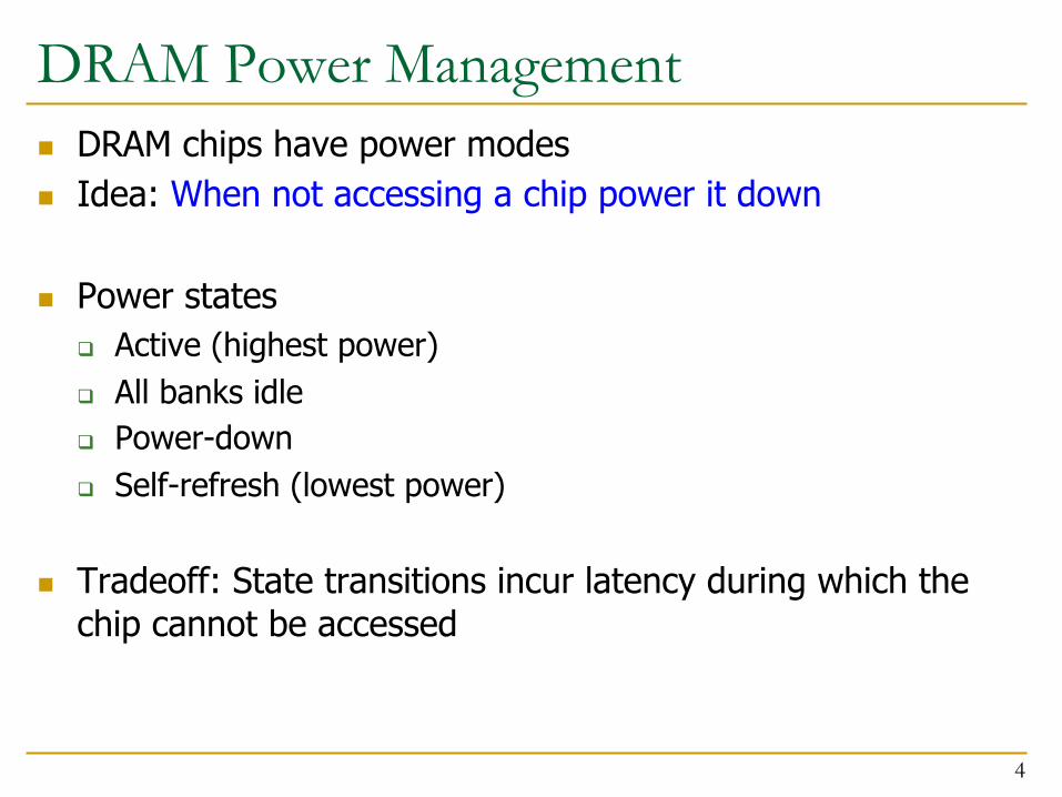
DRAM Power Management n DRAM chips have power modes n Idea: When not accessing a chip power it down
n Power states q Active (highest power) q All banks idle q Power-down q Self-refresh (lowest power)
n Tradeoff: State transitions incur latency during which the chip cannot be accessed
4
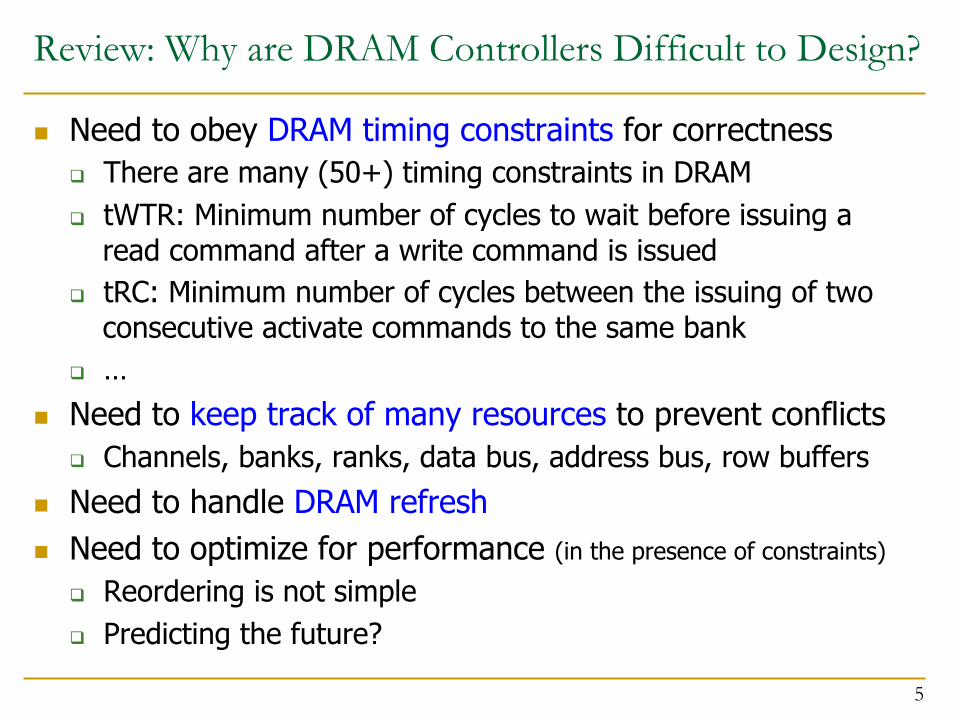
Review: Why are DRAM Controllers Difficult to Design?
n Need to obey DRAM timing constraints for correctness q There are many (50+) timing constraints in DRAM q tWTR: Minimum number of cycles to wait before issuing a
read command after a write command is issued q tRC: Minimum number of cycles between the issuing of two
consecutive activate commands to the same bank q …
n Need to keep track of many resources to prevent conflicts q Channels, banks, ranks, data bus, address bus, row buffers
n Need to handle DRAM refresh n Need to optimize for performance (in the presence of constraints)
q Reordering is not simple q Predicting the future?
5
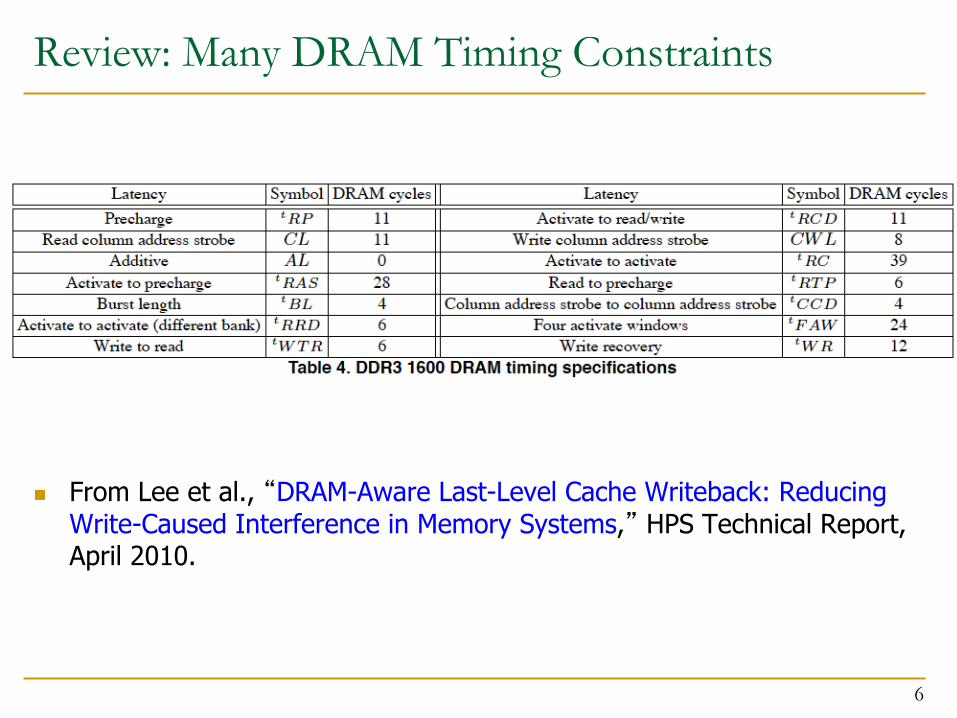
Review: Many DRAM Timing Constraints
n From Lee et al., “DRAM-Aware Last-Level Cache Writeback: Reducing Write-Caused Interference in Memory Systems,” HPS Technical Report, April 2010.
6
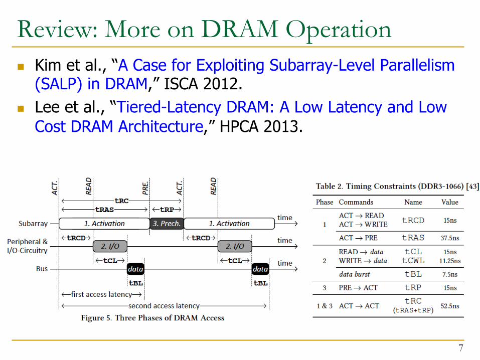
Review: More on DRAM Operation n Kim et al., “A Case for Exploiting Subarray-Level Parallelism
(SALP) in DRAM,” ISCA 2012. n Lee et al., “Tiered-Latency DRAM: A Low Latency and Low
Cost DRAM Architecture,” HPCA 2013.
7
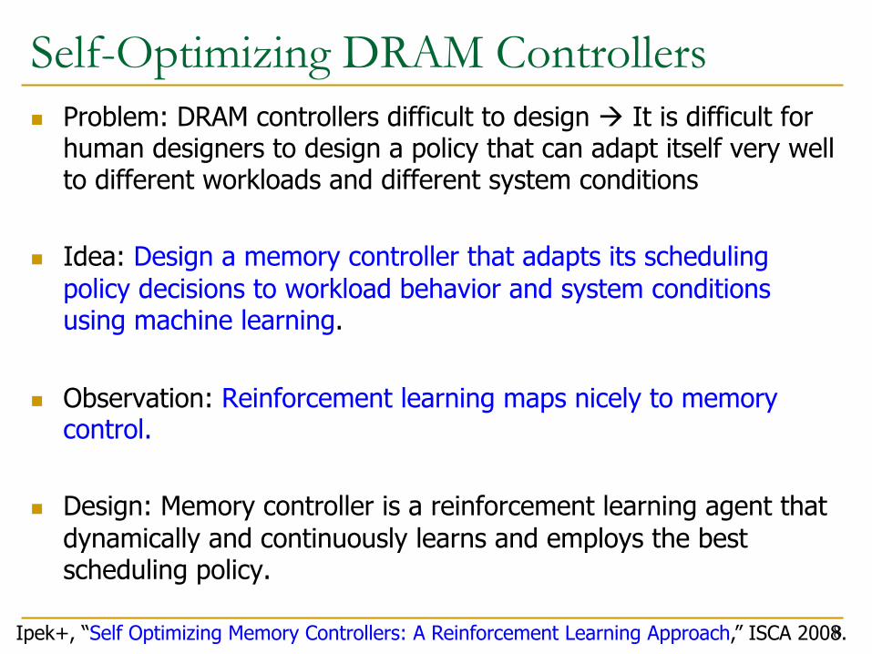
Self-Optimizing DRAM Controllers n Problem: DRAM controllers difficult to design à It is difficult for
human designers to design a policy that can adapt itself very well to different workloads and different system conditions
n Idea: Design a memory controller that adapts its scheduling policy decisions to workload behavior and system conditions using machine learning.
n Observation: Reinforcement learning maps nicely to memory control.
n Design: Memory controller is a reinforcement learning agent that dynamically and continuously learns and employs the best scheduling policy.
8 Ipek+, “Self Optimizing Memory Controllers: A Reinforcement Learning Approach,” ISCA 2008.
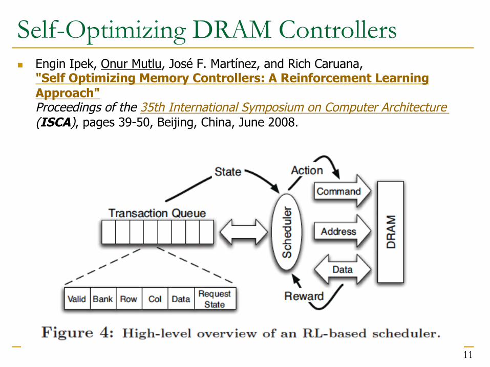
Self-Optimizing DRAM Controllers n Engin Ipek, Onur Mutlu, José F. Martínez, and Rich
Caruana, "Self Optimizing Memory Controllers: A Reinforcement Learning Approach" Proceedings of the 35th International Symposium on Computer Architecture (ISCA), pages 39-50, Beijing, China, June 2008.
9
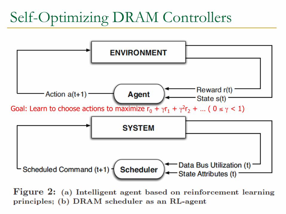
Goal: Learn to choose actions to maximize r0 + γr1 + γ2r2 + … ( 0 ≤ γ < 1)
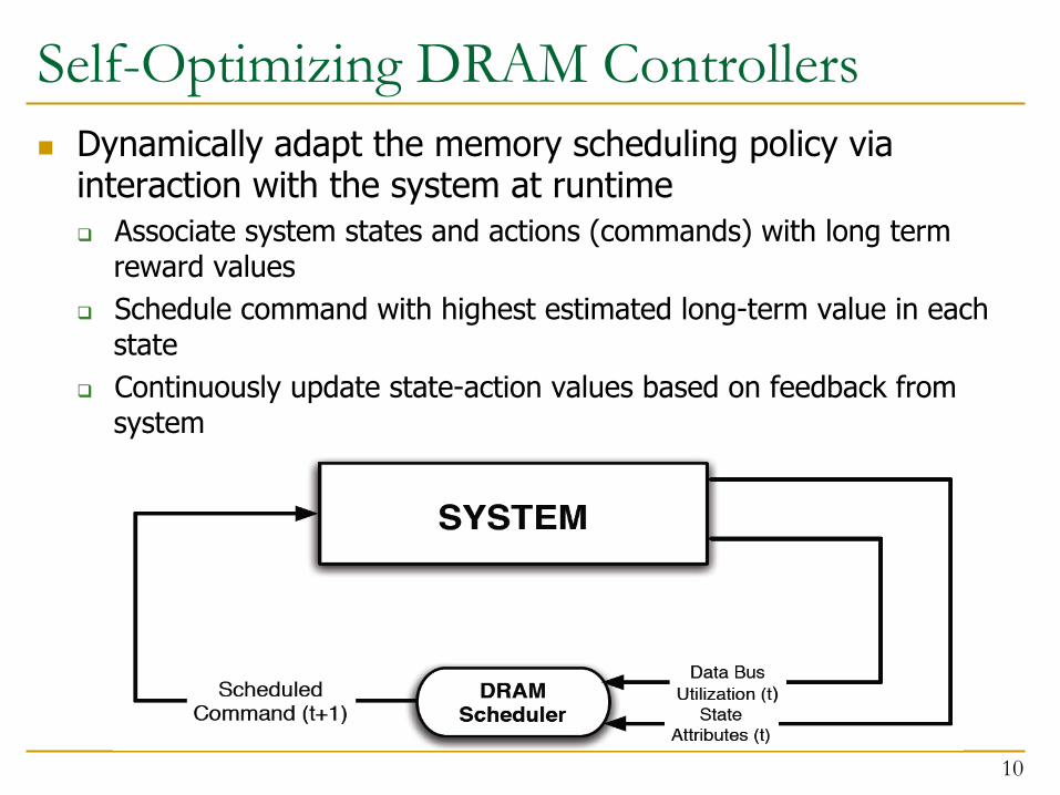
Self-Optimizing DRAM Controllers n Dynamically adapt the memory scheduling policy via
interaction with the system at runtime q Associate system states and actions (commands) with long term
reward values q Schedule command with highest estimated long-term value in each
state q Continuously update state-action values based on feedback from
system
10
Self-Optimizing DRAM Controllers n Engin Ipek, Onur Mutlu, José F. Martínez, and Rich Caruana,
"Self Optimizing Memory Controllers: A Reinforcement Learning Approach" Proceedings of the 35th International Symposium on Computer Architecture (ISCA), pages 39-50, Beijing, China, June 2008.
11
States, Actions, Rewards
12
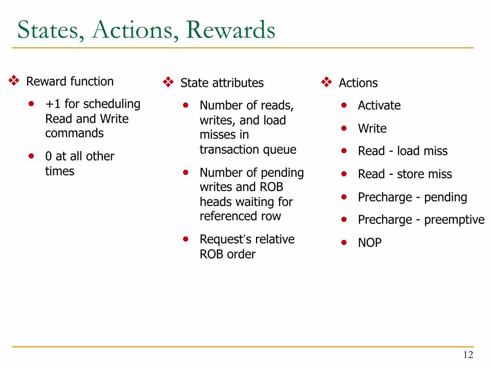
❖ Reward function
• +1 for scheduling Read and Write commands
• 0 at all other times
❖ State attributes
• Number of reads, writes, and load misses in transaction queue
• Number of pending writes and ROB heads waiting for referenced row
• Request’s relative ROB order
❖ Actions
• Activate
• Write
• Read - load miss
• Read - store miss
• Precharge - pending
• Precharge - preemptive
• NOP
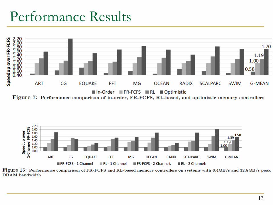
Performance Results
13
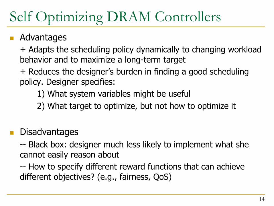
Self Optimizing DRAM Controllers n Advantages
+ Adapts the scheduling policy dynamically to changing workload behavior and to maximize a long-term target + Reduces the designer’s burden in finding a good scheduling policy. Designer specifies:
1) What system variables might be useful 2) What target to optimize, but not how to optimize it
n Disadvantages
-- Black box: designer much less likely to implement what she cannot easily reason about -- How to specify different reward functions that can achieve different objectives? (e.g., fairness, QoS)
14
Trends Affecting Main Memory
Agenda for Topic 1 (DRAM Scaling)
n What Will You Learn in This Mini-Lecture Series n Main Memory Basics (with a Focus on DRAM) n Major Trends Affecting Main Memory n DRAM Scaling Problem and Solution Directions n Solution Direction 1: System-DRAM Co-Design n Ongoing Research n Summary
16
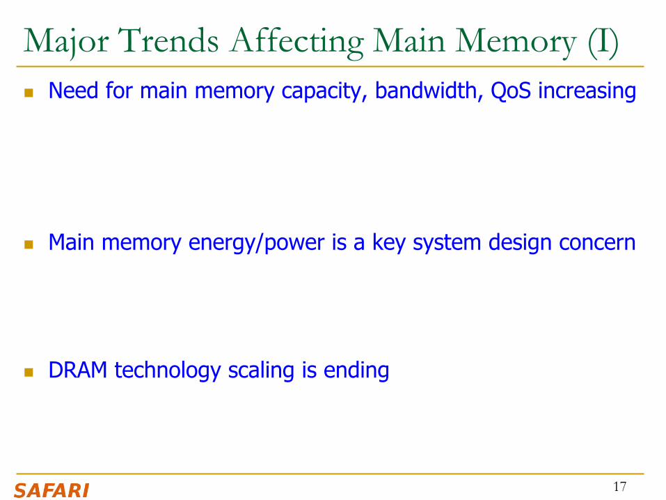
Major Trends Affecting Main Memory (I) n Need for main memory capacity, bandwidth, QoS increasing
n Main memory energy/power is a key system design concern
n DRAM technology scaling is ending
17
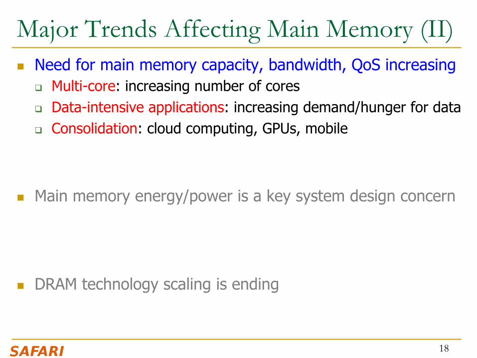
Major Trends Affecting Main Memory (II) n Need for main memory capacity, bandwidth, QoS increasing
q Multi-core: increasing number of cores q Data-intensive applications: increasing demand/hunger for data q Consolidation: cloud computing, GPUs, mobile
n Main memory energy/power is a key system design concern
n DRAM technology scaling is ending
18
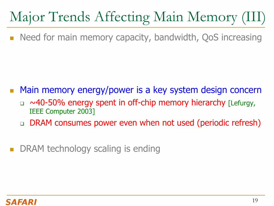
Major Trends Affecting Main Memory (III) n Need for main memory capacity, bandwidth, QoS increasing
n Main memory energy/power is a key system design concern
q ~40-50% energy spent in off-chip memory hierarchy [Lefurgy, IEEE Computer 2003]
q DRAM consumes power even when not used (periodic refresh)
n DRAM technology scaling is ending
19
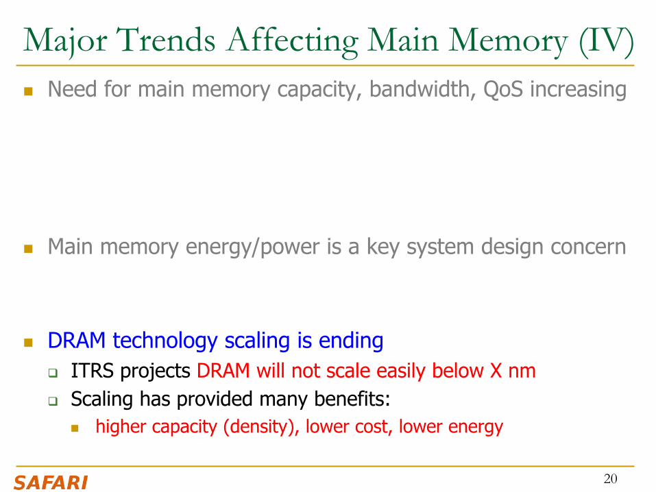
Major Trends Affecting Main Memory (IV) n Need for main memory capacity, bandwidth, QoS increasing
n Main memory energy/power is a key system design concern
n DRAM technology scaling is ending
q ITRS projects DRAM will not scale easily below X nm q Scaling has provided many benefits:
n higher capacity (density), lower cost, lower energy
20
Agenda for Today
n What Will You Learn in This Mini-Lecture Series n Main Memory Basics (with a Focus on DRAM) n Major Trends Affecting Main Memory n DRAM Scaling Problem and Solution Directions n Solution Direction 1: System-DRAM Co-Design n Ongoing Research n Summary
21
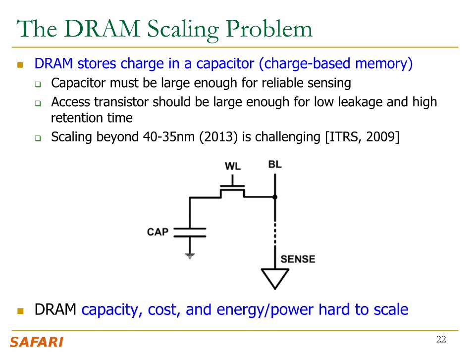
The DRAM Scaling Problem n DRAM stores charge in a capacitor (charge-based memory)
q Capacitor must be large enough for reliable sensing q Access transistor should be large enough for low leakage and high
retention time q Scaling beyond 40-35nm (2013) is challenging [ITRS, 2009]
n DRAM capacity, cost, and energy/power hard to scale
22
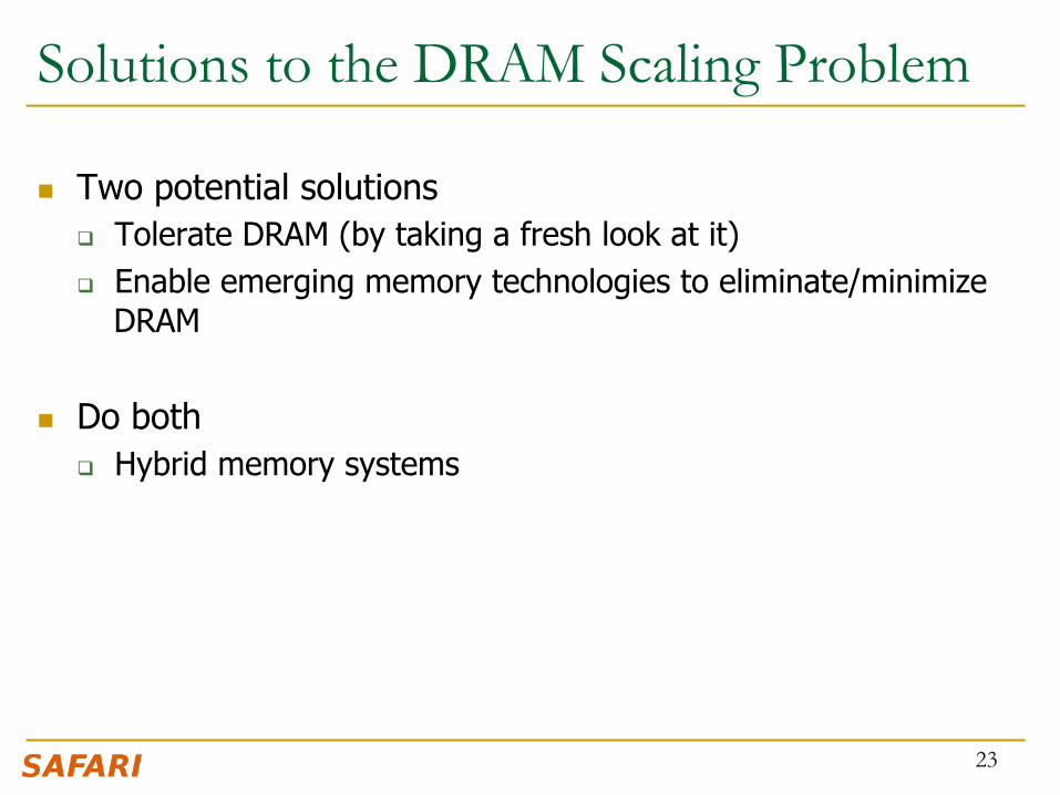
Solutions to the DRAM Scaling Problem
n Two potential solutions q Tolerate DRAM (by taking a fresh look at it) q Enable emerging memory technologies to eliminate/minimize
DRAM
n Do both q Hybrid memory systems
23
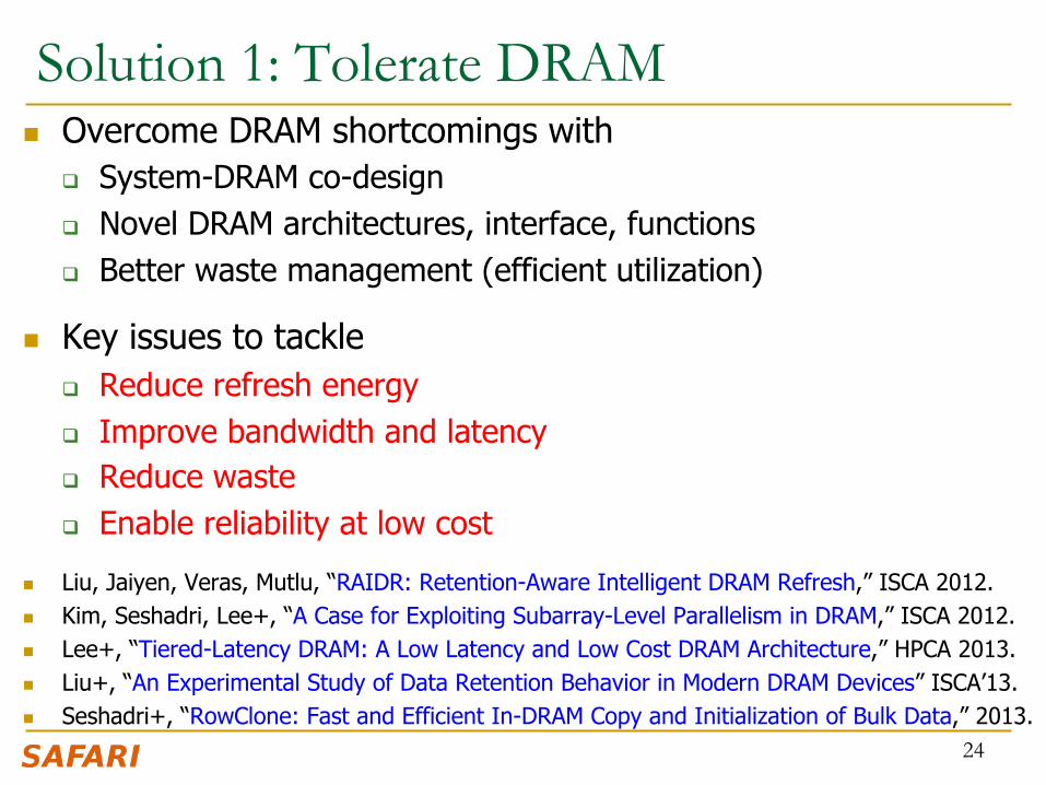
Solution 1: Tolerate DRAM n Overcome DRAM shortcomings with
q System-DRAM co-design q Novel DRAM architectures, interface, functions q Better waste management (efficient utilization)
n Key issues to tackle q Reduce refresh energy q Improve bandwidth and latency q Reduce waste q Enable reliability at low cost
n Liu, Jaiyen, Veras, Mutlu, “RAIDR: Retention-Aware Intelligent DRAM Refresh,” ISCA 2012. n Kim, Seshadri, Lee+, “A Case for Exploiting Subarray-Level Parallelism in DRAM,” ISCA 2012. n Lee+, “Tiered-Latency DRAM: A Low Latency and Low Cost DRAM Architecture,” HPCA 2013. n Liu+, “An Experimental Study of Data Retention Behavior in Modern DRAM Devices” ISCA’13. n Seshadri+, “RowClone: Fast and Efficient In-DRAM Copy and Initialization of Bulk Data,” 2013.
24
Tolerating DRAM: System-DRAM Co-Design
New DRAM Architectures
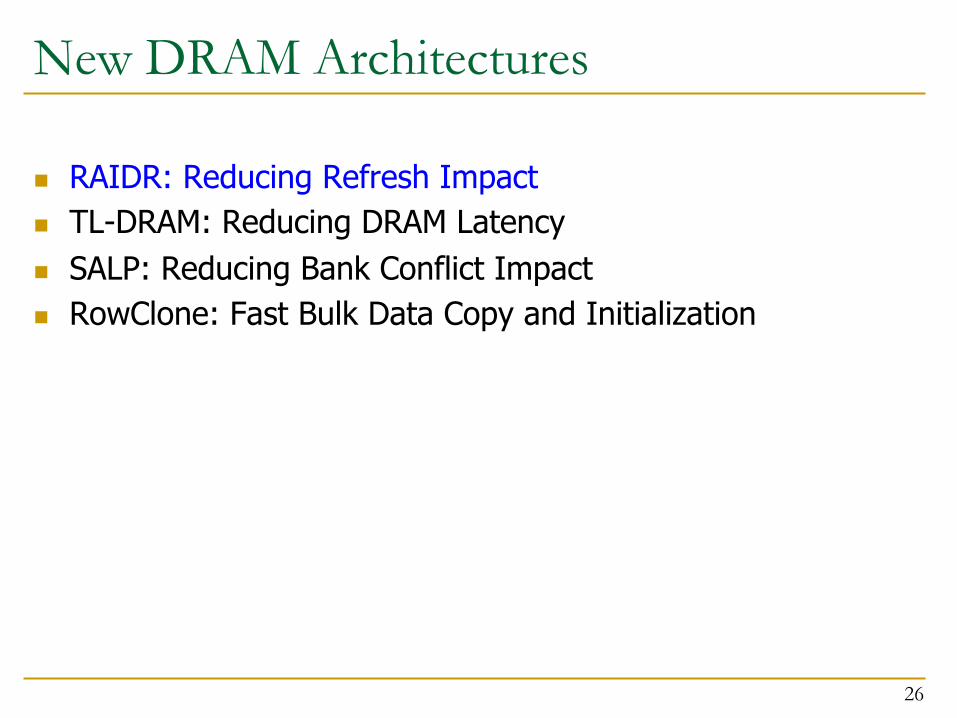
n RAIDR: Reducing Refresh Impact n TL-DRAM: Reducing DRAM Latency n SALP: Reducing Bank Conflict Impact n RowClone: Fast Bulk Data Copy and Initialization
26
RAIDR: Reducing DRAM Refresh Impact
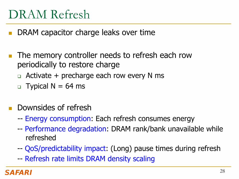
DRAM Refresh n DRAM capacitor charge leaks over time
n The memory controller needs to refresh each row periodically to restore charge q Activate + precharge each row every N ms q Typical N = 64 ms
n Downsides of refresh -- Energy consumption: Each refresh consumes energy
-- Performance degradation: DRAM rank/bank unavailable while refreshed
-- QoS/predictability impact: (Long) pause times during refresh -- Refresh rate limits DRAM density scaling 28
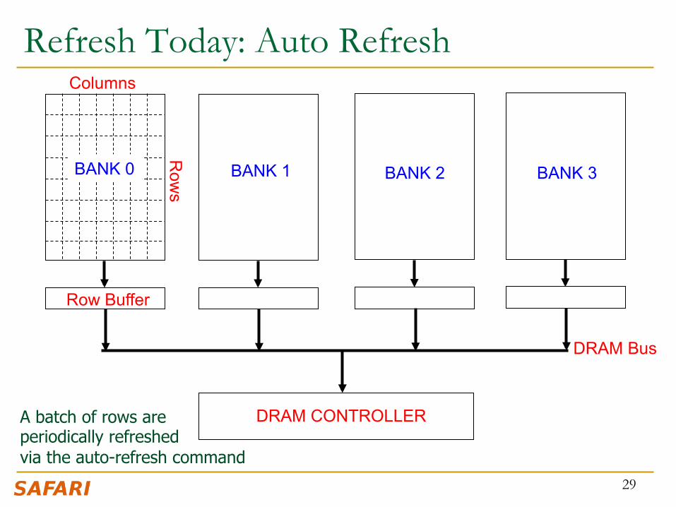
Refresh Today: Auto Refresh
29
Columns
Row
s
Row Buffer
DRAM CONTROLLER
DRAM Bus
BANK 0 BANK 1 BANK 2 BANK 3
A batch of rows are periodically refreshed via the auto-refresh command
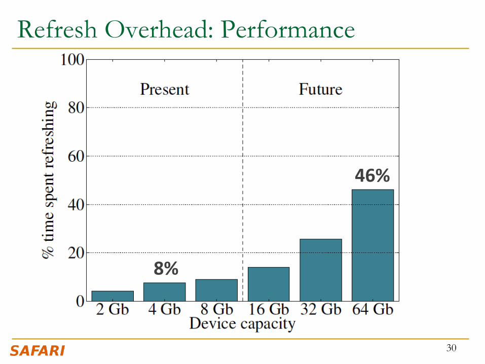
Refresh Overhead: Performance
30
8%
46%
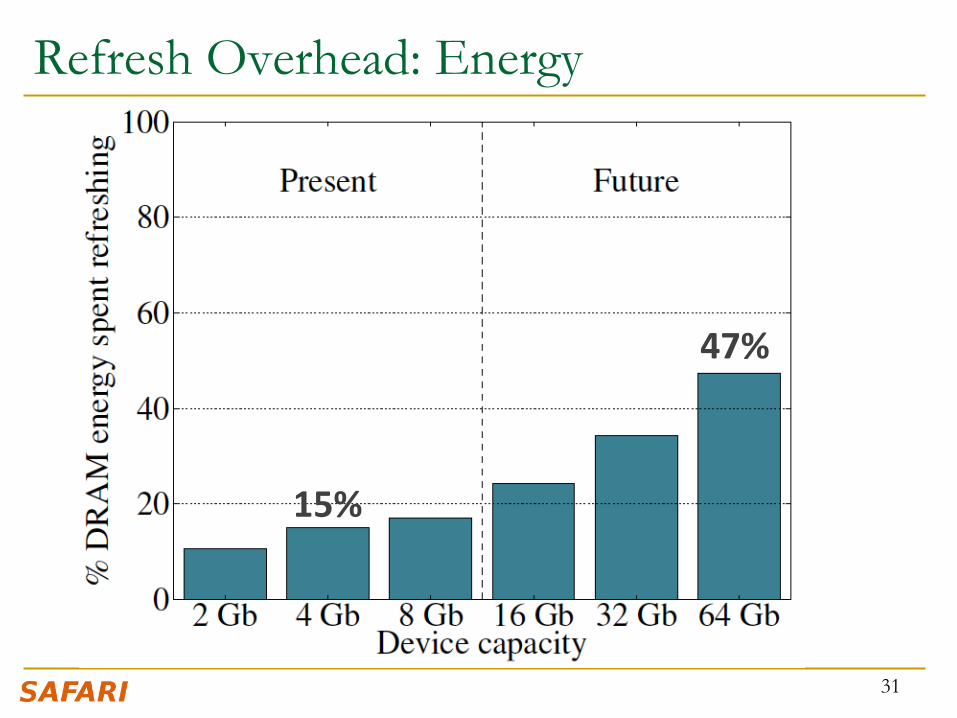
Refresh Overhead: Energy
31
15%
47%
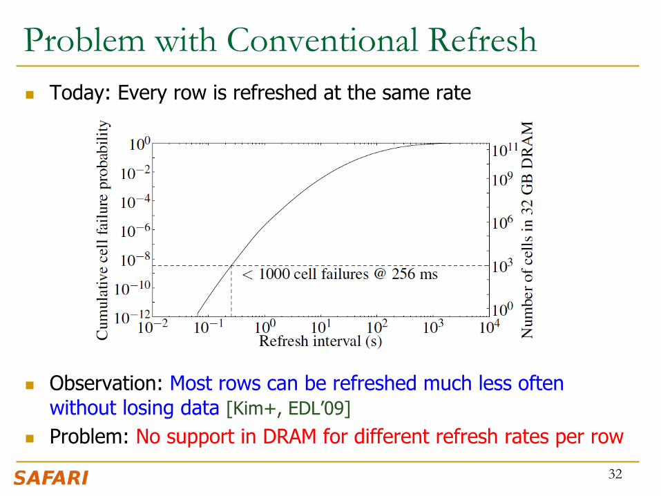
Problem with Conventional Refresh n Today: Every row is refreshed at the same rate
n Observation: Most rows can be refreshed much less often without losing data [Kim+, EDL’09]
n Problem: No support in DRAM for different refresh rates per row
32
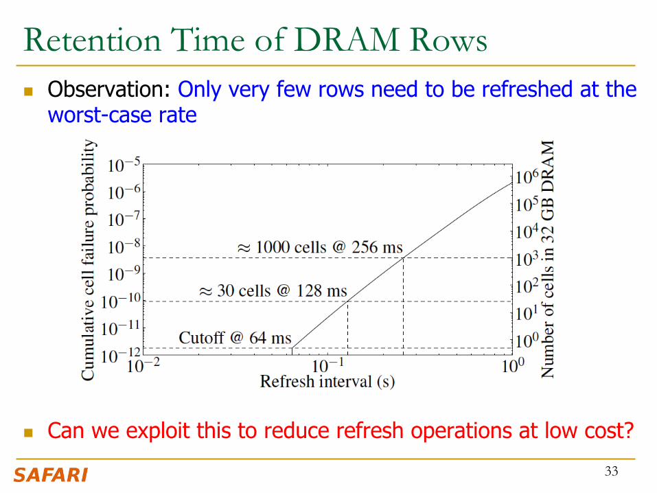
Retention Time of DRAM Rows n Observation: Only very few rows need to be refreshed at the
worst-case rate
n Can we exploit this to reduce refresh operations at low cost?
33
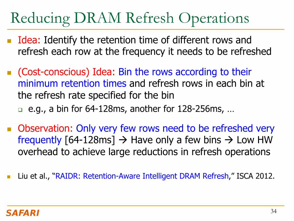
Reducing DRAM Refresh Operations n Idea: Identify the retention time of different rows and
refresh each row at the frequency it needs to be refreshed
n (Cost-conscious) Idea: Bin the rows according to their minimum retention times and refresh rows in each bin at the refresh rate specified for the bin q e.g., a bin for 64-128ms, another for 128-256ms, …
n Observation: Only very few rows need to be refreshed very frequently [64-128ms] à Have only a few bins à Low HW overhead to achieve large reductions in refresh operations
n Liu et al., “RAIDR: Retention-Aware Intelligent DRAM Refresh,” ISCA 2012.
34
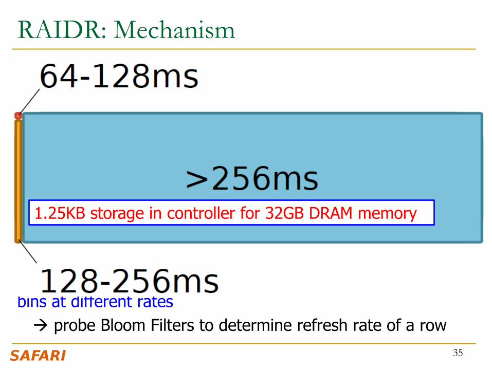
1. Profiling: Profile the retention time of all DRAM rows à can be done at DRAM design time or dynamically 2. Binning: Store rows into bins by retention time à use Bloom Filters for efficient and scalable storage 3. Refreshing: Memory controller refreshes rows in different bins at different rates à probe Bloom Filters to determine refresh rate of a row
RAIDR: Mechanism
35
1.25KB storage in controller for 32GB DRAM memory
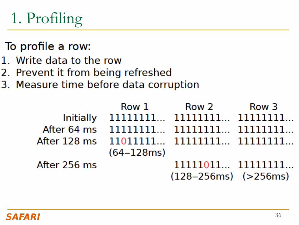
1. Profiling
36
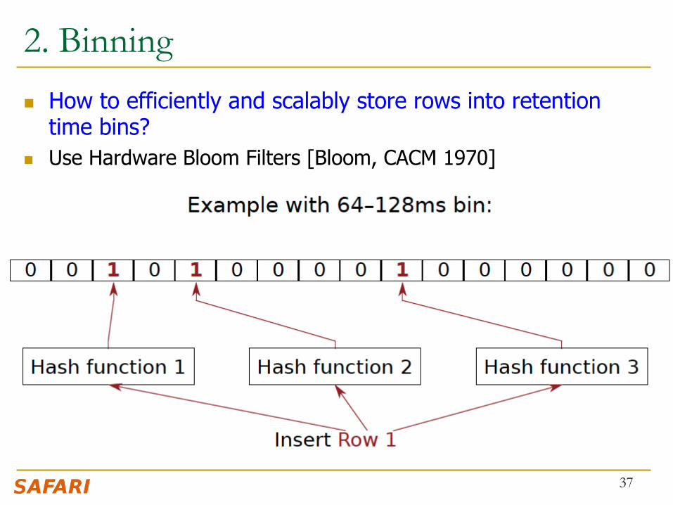
2. Binning
n How to efficiently and scalably store rows into retention time bins?
n Use Hardware Bloom Filters [Bloom, CACM 1970]
37
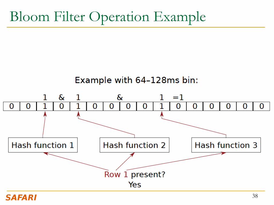
Bloom Filter Operation Example
38
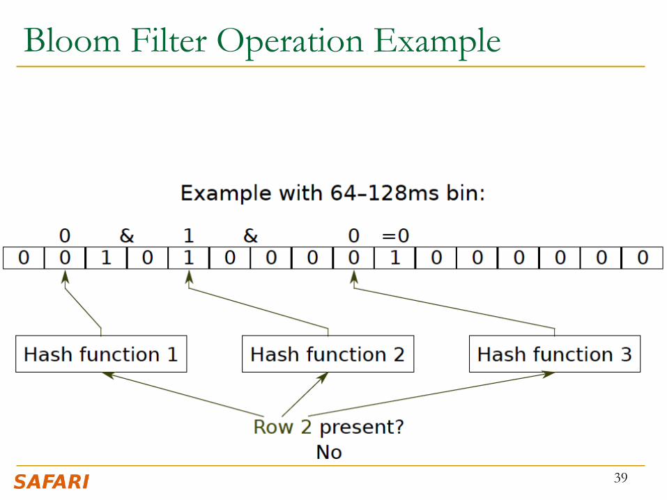
Bloom Filter Operation Example
39
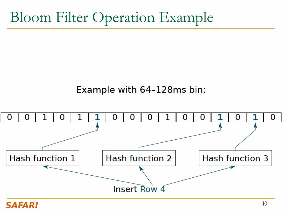
Bloom Filter Operation Example
40
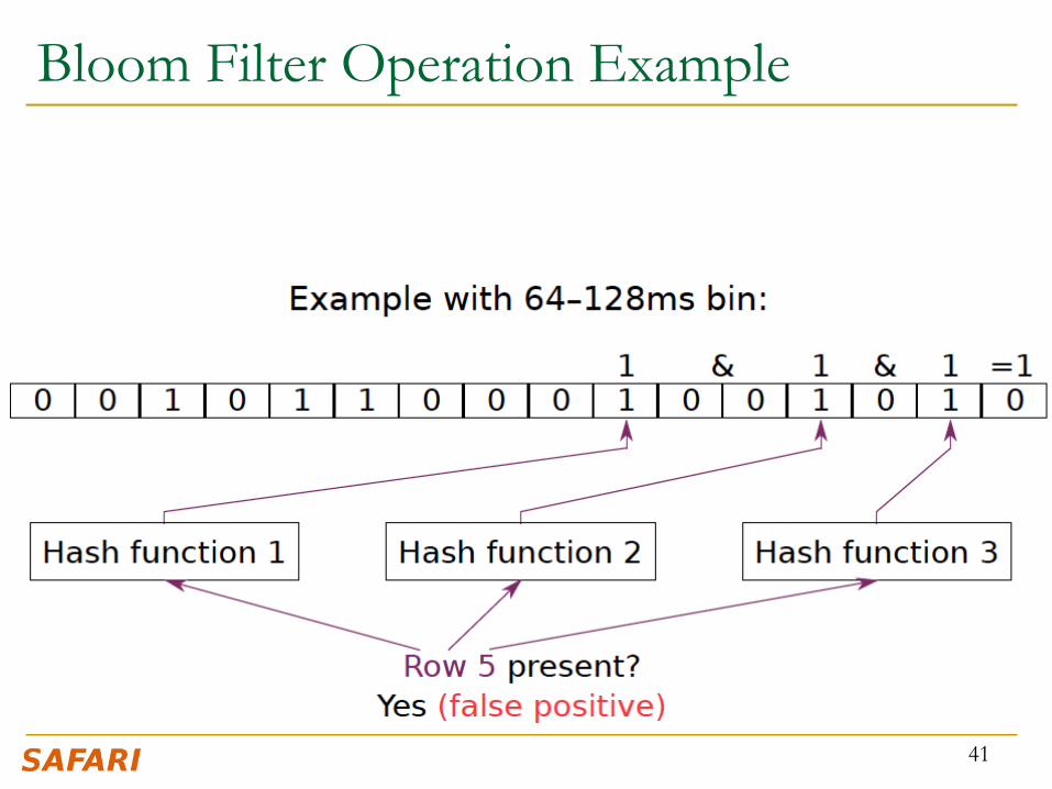
Bloom Filter Operation Example
41
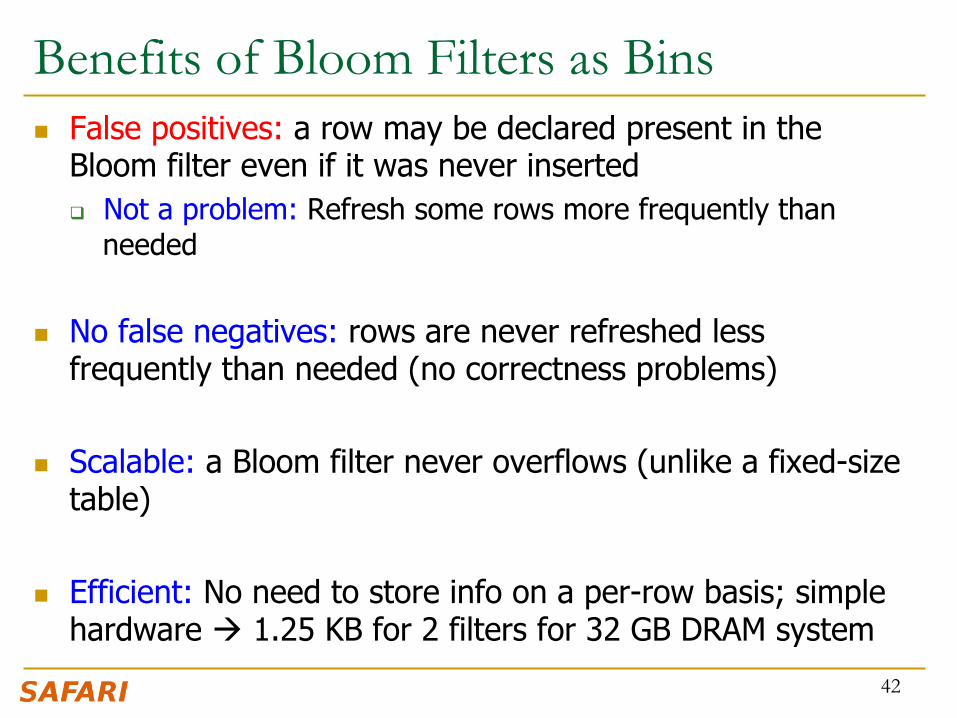
Benefits of Bloom Filters as Bins n False positives: a row may be declared present in the
Bloom filter even if it was never inserted q Not a problem: Refresh some rows more frequently than
needed
n No false negatives: rows are never refreshed less frequently than needed (no correctness problems)
n Scalable: a Bloom filter never overflows (unlike a fixed-size table)
n Efficient: No need to store info on a per-row basis; simple hardware à 1.25 KB for 2 filters for 32 GB DRAM system
42
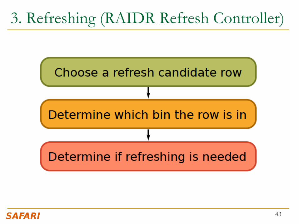
3. Refreshing (RAIDR Refresh Controller)
43
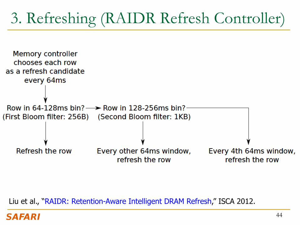
3. Refreshing (RAIDR Refresh Controller)
44
Liu et al., “RAIDR: Retention-Aware Intelligent DRAM Refresh,” ISCA 2012.
Tolerating Temperature Changes
45
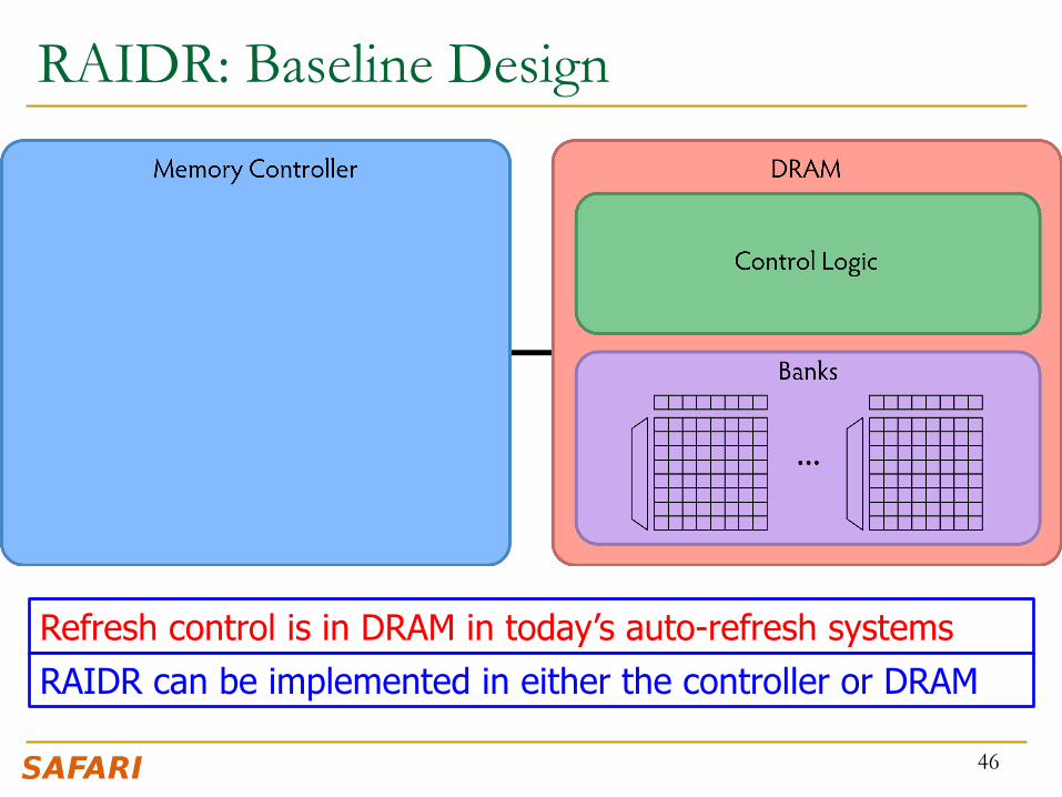
RAIDR: Baseline Design
46
Refresh control is in DRAM in today’s auto-refresh systems RAIDR can be implemented in either the controller or DRAM
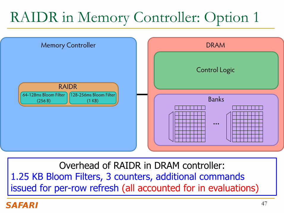
RAIDR in Memory Controller: Option 1
47
Overhead of RAIDR in DRAM controller: 1.25 KB Bloom Filters, 3 counters, additional commands issued for per-row refresh (all accounted for in evaluations)
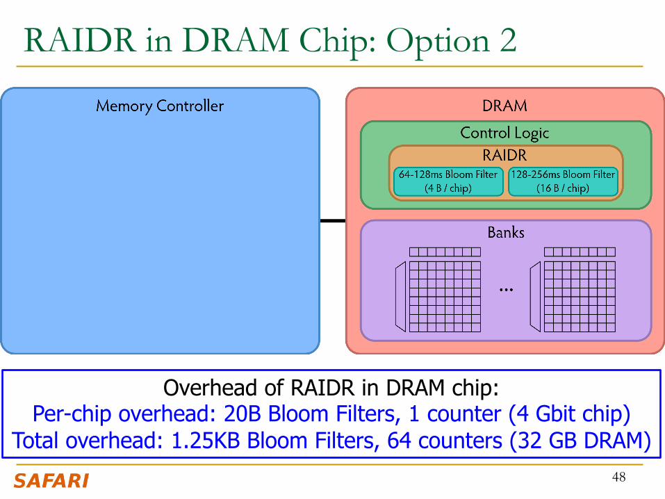
RAIDR in DRAM Chip: Option 2
48
Overhead of RAIDR in DRAM chip: Per-chip overhead: 20B Bloom Filters, 1 counter (4 Gbit chip)
Total overhead: 1.25KB Bloom Filters, 64 counters (32 GB DRAM)
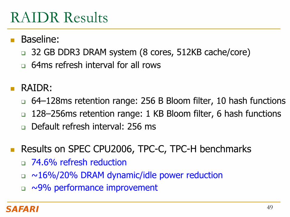
RAIDR Results n Baseline:
q 32 GB DDR3 DRAM system (8 cores, 512KB cache/core) q 64ms refresh interval for all rows
n RAIDR: q 64–128ms retention range: 256 B Bloom filter, 10 hash functions q 128–256ms retention range: 1 KB Bloom filter, 6 hash functions q Default refresh interval: 256 ms
n Results on SPEC CPU2006, TPC-C, TPC-H benchmarks q 74.6% refresh reduction q ~16%/20% DRAM dynamic/idle power reduction q ~9% performance improvement
49
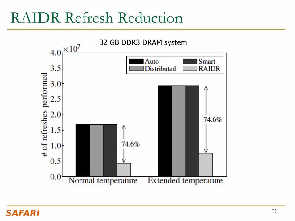
RAIDR Refresh Reduction
50
32 GB DDR3 DRAM system
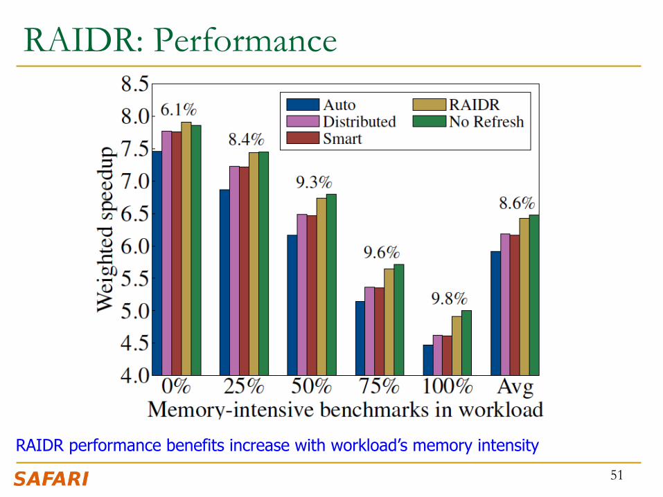
RAIDR: Performance
51
RAIDR performance benefits increase with workload’s memory intensity
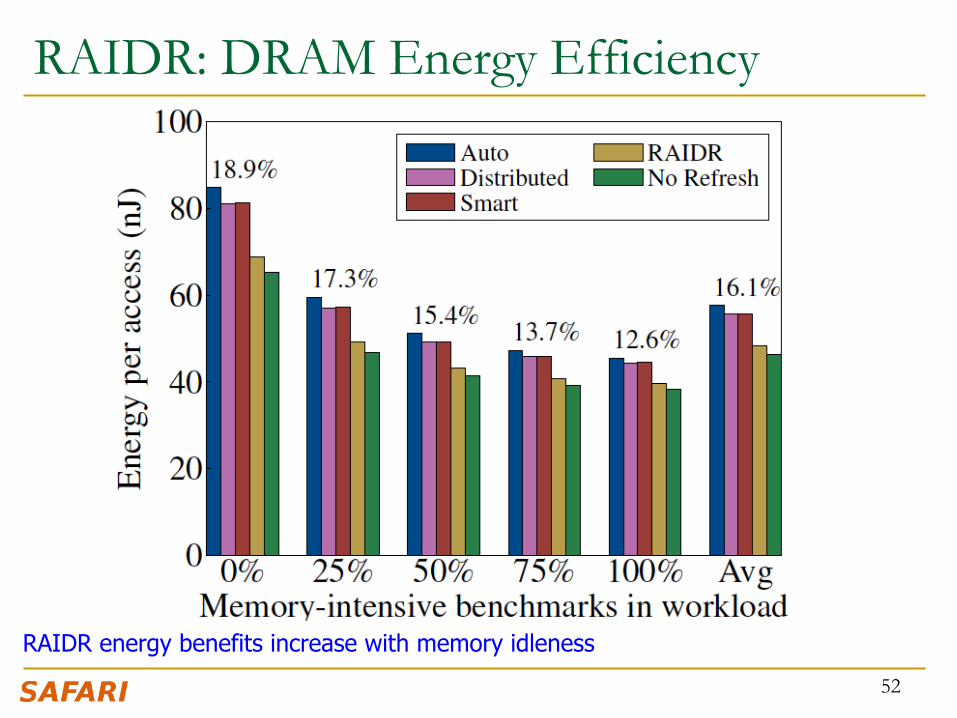
RAIDR: DRAM Energy Efficiency
52
RAIDR energy benefits increase with memory idleness
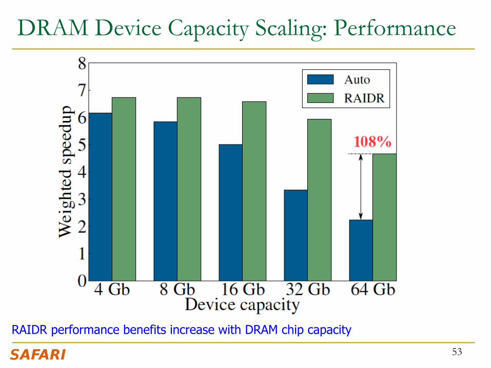
DRAM Device Capacity Scaling: Performance
53
RAIDR performance benefits increase with DRAM chip capacity
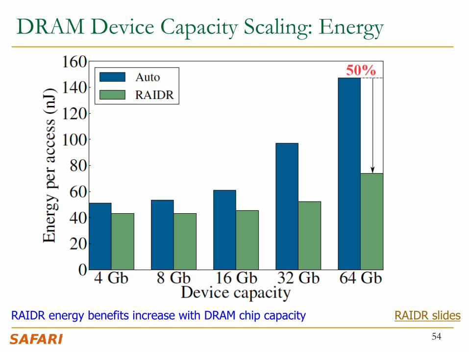
DRAM Device Capacity Scaling: Energy
54
RAIDR energy benefits increase with DRAM chip capacity RAIDR slides
More Readings Related to RAIDR
n Jamie Liu, Ben Jaiyen, Yoongu Kim, Chris Wilkerson, and Onur Mutlu, "An Experimental Study of Data Retention Behavior in Modern DRAM Devices: Implications for Retention Time Profiling Mechanisms" Proceedings of the 40th International Symposium on Computer Architecture (ISCA), Tel-Aviv, Israel, June 2013. Slides (pptx) Slides (pdf)
55
New DRAM Architectures
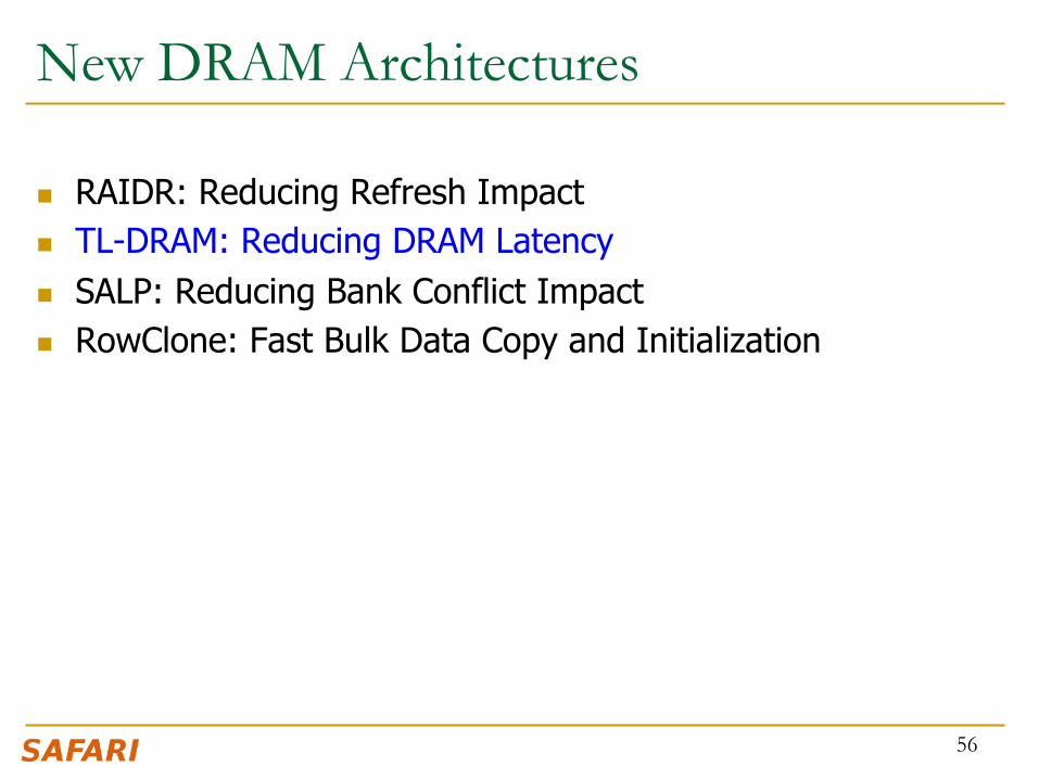
n RAIDR: Reducing Refresh Impact n TL-DRAM: Reducing DRAM Latency n SALP: Reducing Bank Conflict Impact n RowClone: Fast Bulk Data Copy and Initialization
56
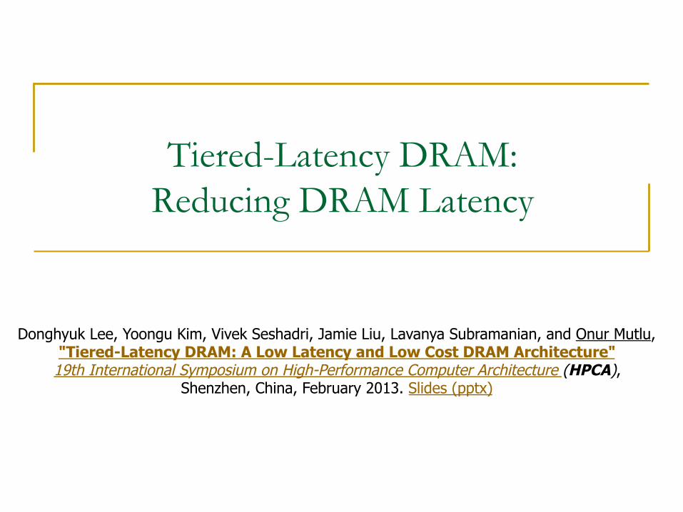
Tiered-Latency DRAM: Reducing DRAM Latency
Donghyuk Lee, Yoongu Kim, Vivek Seshadri, Jamie Liu, Lavanya Subramanian, and Onur Mutlu, "Tiered-Latency DRAM: A Low Latency and Low Cost DRAM Architecture" 19th International Symposium on High-Performance Computer Architecture (HPCA),
Shenzhen, China, February 2013. Slides (pptx)
58
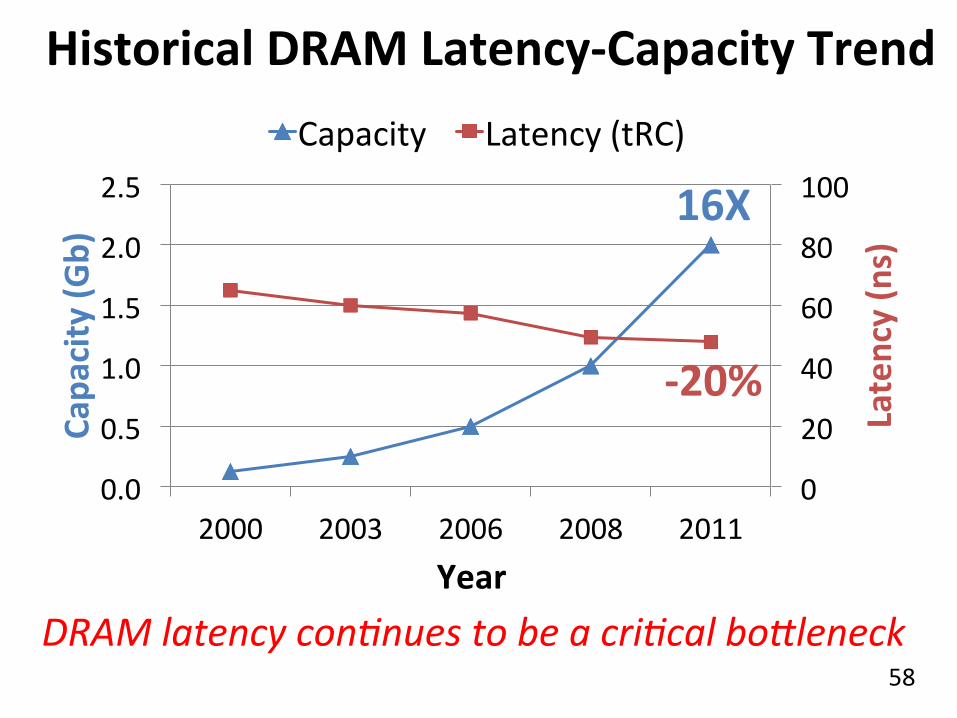
Historical DRAM Latency-‐Capacity Trend
0
20
40
60
80
100
0.0
0.5
1.0
1.5
2.0
2.5
2000 2003 2006 2008 2011
Latency (ns)
Capa
city (G
b)
Year
Capacity Latency (tRC)
16X
-‐20%
DRAM latency con.nues to be a cri.cal bo4leneck
59
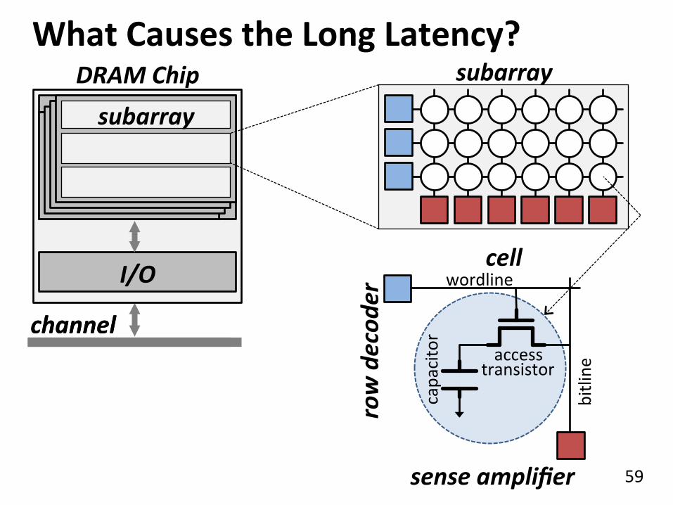
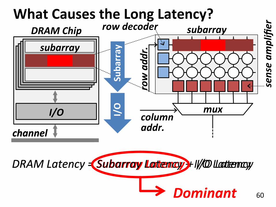
What Causes the Long Latency? DRAM Chip
channel
I/O
channel
I/O
cell array cell array
banks subarray
subarray
row decod
er
sense amplifier
capacitor
access transistor
wordline
bitline
cell
60
DRAM Chip
channel
I/O
channel
I/O
cell array cell array
banks subarray
subarray What Causes the Long Latency?
DRAM Latency = Subarray Latency + I/O Latency DRAM Latency = Subarray Latency + I/O Latency
Dominant
Suba
rray
I/O
row add
r.
row decoder
sense am
plifier
mux column addr.
61
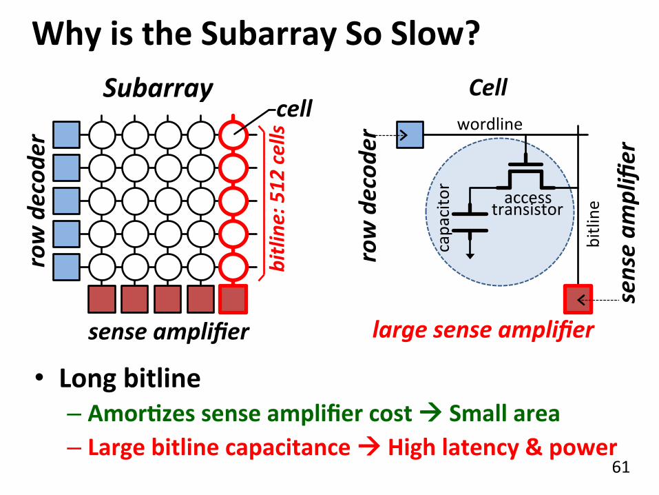
Why is the Subarray So Slow? Subarray
row decod
er
sense amplifier
capacitor
access transistor
wordline
bitline
Cell
large sense amplifier
bitline
: 512 cells cell
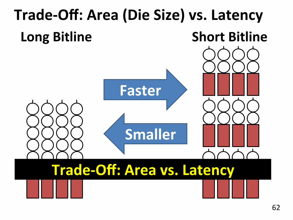
• Long bitline – AmorRzes sense amplifier cost à Small area – Large bitline capacitance à High latency & power
sense am
plifier
row decod
er
62
Trade-‐Off: Area (Die Size) vs. Latency
Faster
Smaller
Short Bitline
Long Bitline
Trade-‐Off: Area vs. Latency
63
Trade-‐Off: Area (Die Size) vs. Latency
0
1
2
3
4
0 10 20 30 40 50 60 70
Normalized
DRA
M Area
Latency (ns)
64
32
128 256 512 cells/bitline
Commodity DRAM
Long Bitline
Cheape
r
Faster
Fancy DRAM Short Bitline
64
Short Bitline
Low Latency
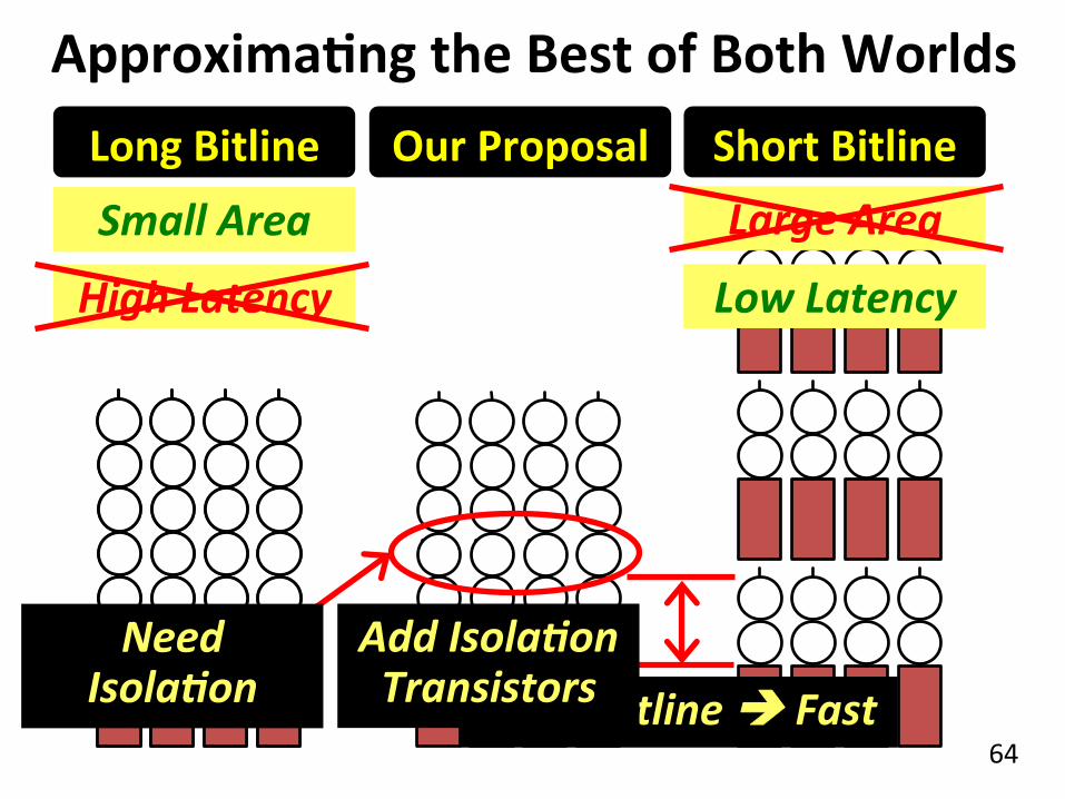
ApproximaRng the Best of Both Worlds Long Bitline
Small Area
Long Bitline
Low Latency
Short Bitline Our Proposal Small Area
Short Bitline è Fast Need
IsolaJon Add IsolaJon Transistors
High Latency
Large Area
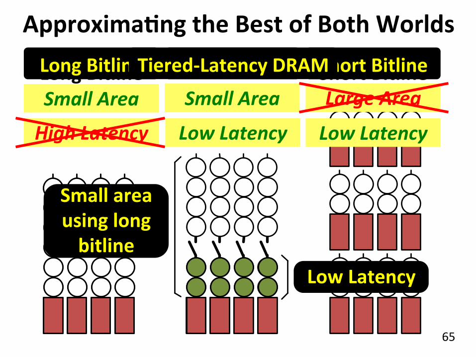
65
ApproximaRng the Best of Both Worlds
Low Latency
Our Proposal Small Area
Long Bitline Small Area
Long Bitline
High Latency
Short Bitline
Low Latency
Short Bitline Large Area
Tiered-‐Latency DRAM
Low Latency
Small area using long bitline
66
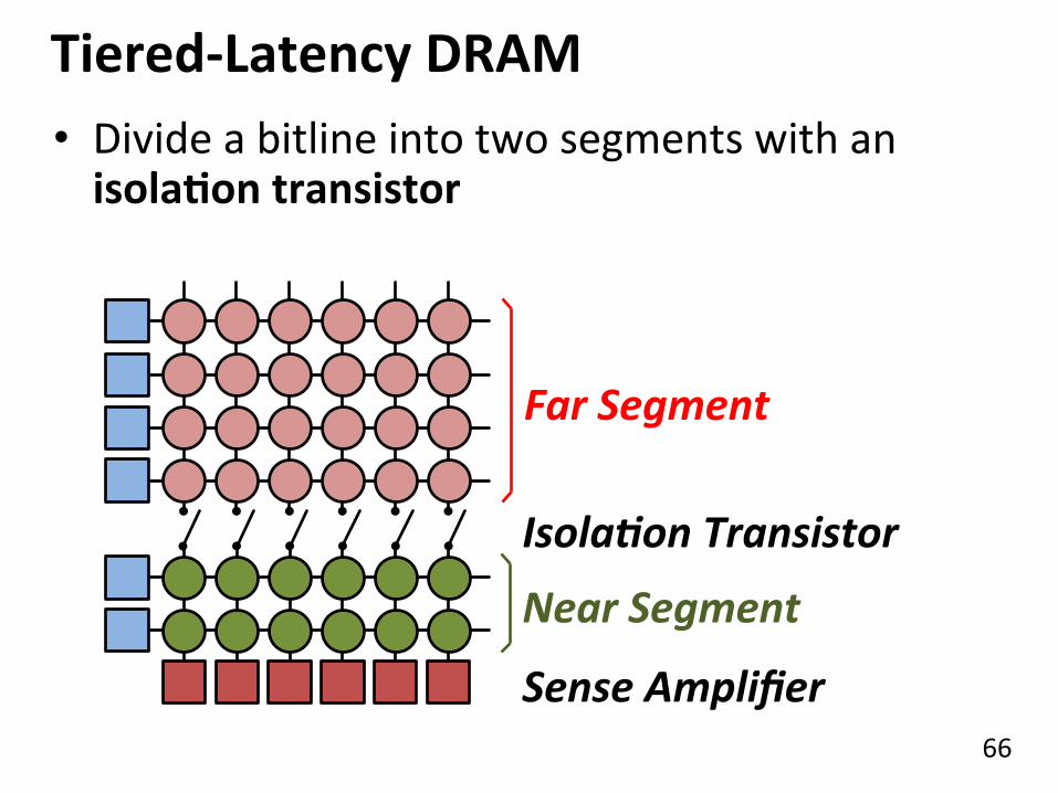
Tiered-‐Latency DRAM
Near Segment
Far Segment
IsolaJon Transistor
• Divide a bitline into two segments with an isolaRon transistor
Sense Amplifier
67
Far Segment Far Segment
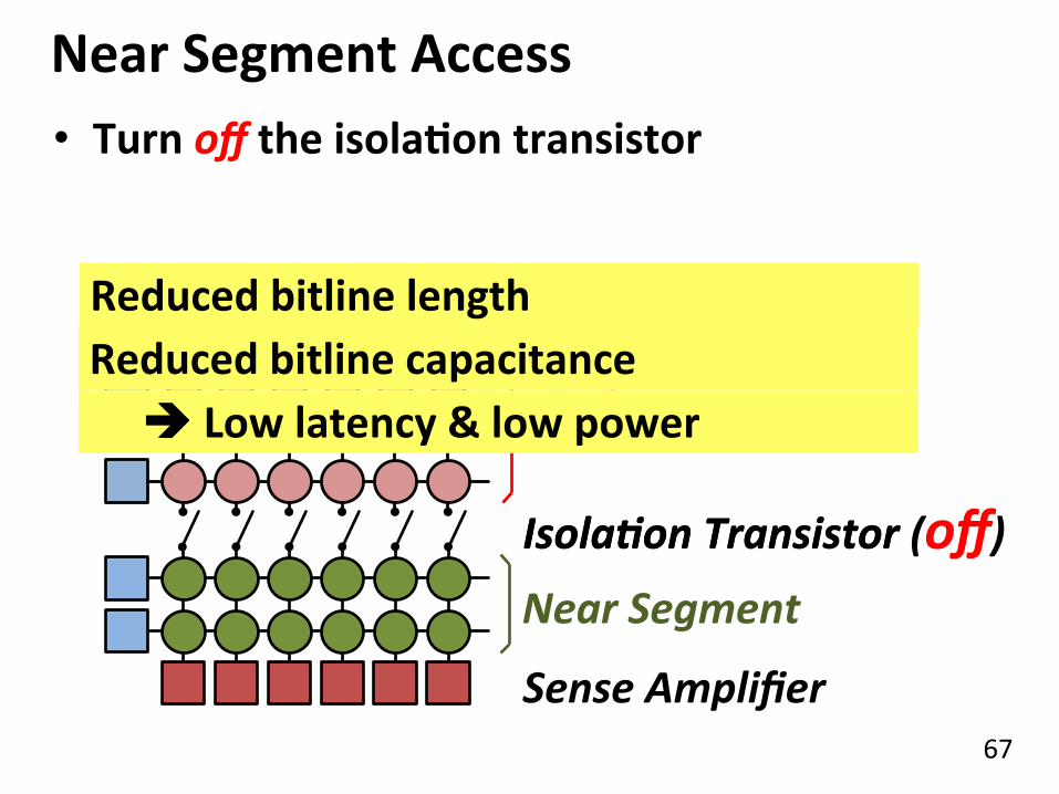
Near Segment Access
Near Segment
IsolaJon Transistor
• Turn off the isolaRon transistor
IsolaJon Transistor (off)
Sense Amplifier
Reduced bitline capacitance è Low latency & low power
Reduced bitline length
68
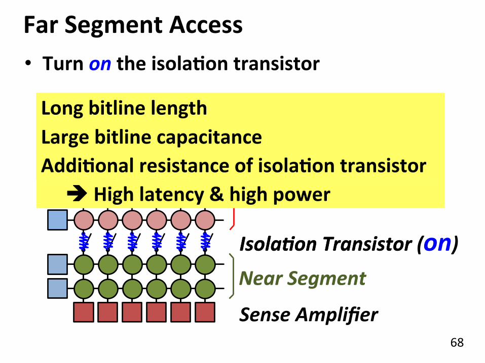
Near Segment Near Segment
Far Segment Access • Turn on the isolaRon transistor
Far Segment
IsolaJon Transistor IsolaJon Transistor (on)
Sense Amplifier
Large bitline capacitance AddiRonal resistance of isolaRon transistor
Long bitline length
è High latency & high power
69
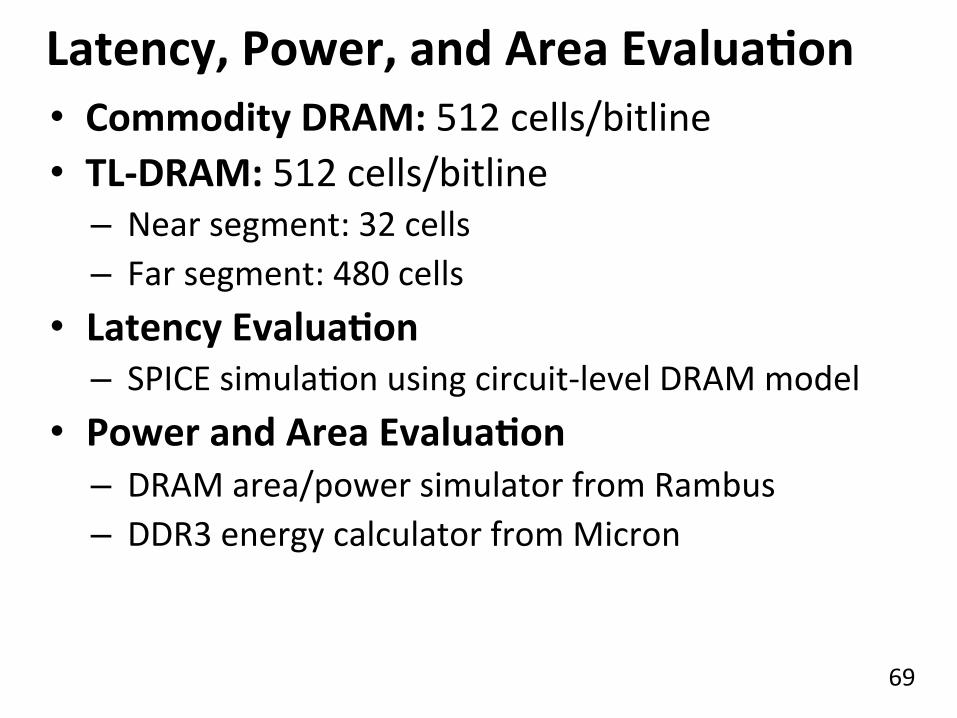
Latency, Power, and Area EvaluaRon • Commodity DRAM: 512 cells/bitline • TL-‐DRAM: 512 cells/bitline
– Near segment: 32 cells – Far segment: 480 cells
• Latency EvaluaRon – SPICE simulaOon using circuit-‐level DRAM model
• Power and Area EvaluaRon – DRAM area/power simulator from Rambus – DDR3 energy calculator from Micron
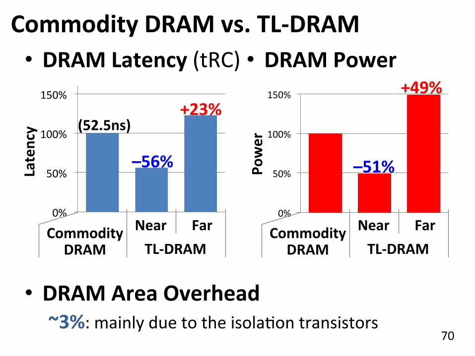
70
0%
50%
100%
150%
0%
50%
100%
150%
Commodity DRAM vs. TL-‐DRAM Latency
Power
–56%
+23%
–51%
+49% • DRAM Latency (tRC) • DRAM Power
• DRAM Area Overhead ~3%: mainly due to the isolaOon transistors
TL-‐DRAM Commodity
DRAM Near Far Commodity
DRAM Near Far TL-‐DRAM
(52.5ns)
71
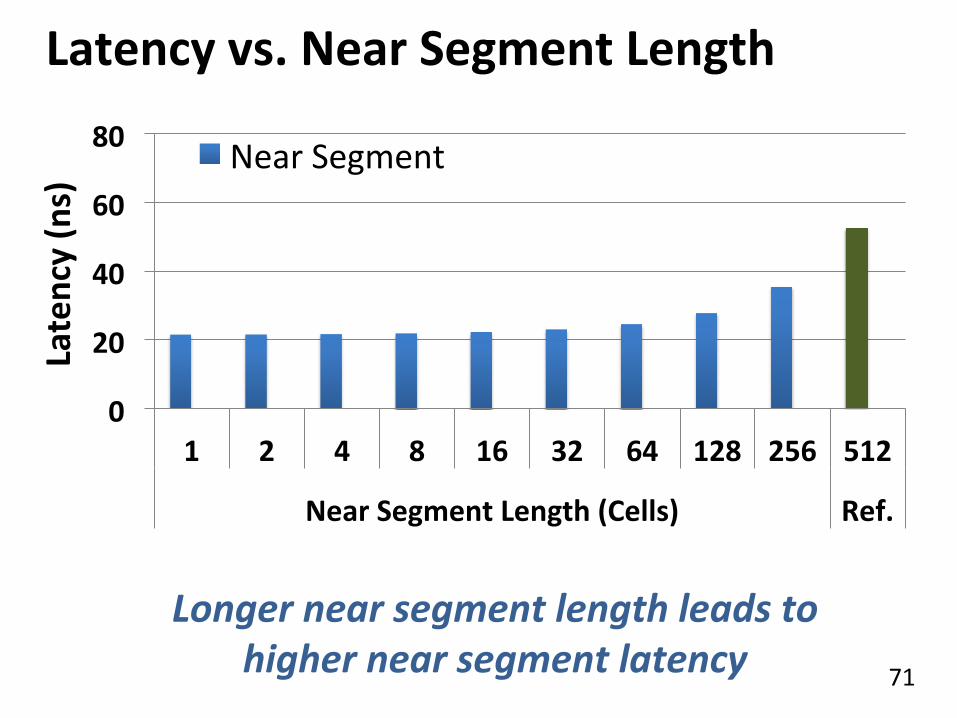
Latency vs. Near Segment Length
0
20
40
60
80
1 2 4 8 16 32 64 128 256 512
Near Segment Length (Cells) Ref.
Near Segment Far Segment
Latency (ns)
Longer near segment length leads to higher near segment latency
72
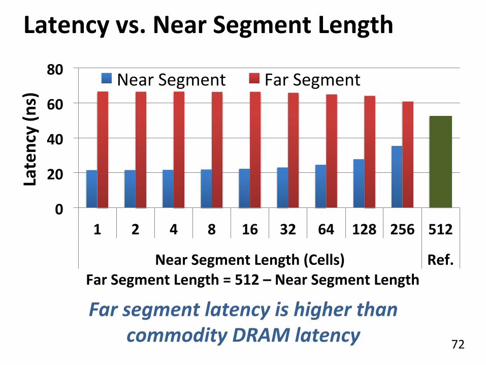
Latency vs. Near Segment Length
0
20
40
60
80
1 2 4 8 16 32 64 128 256 512
Near Segment Length (Cells) Ref.
Near Segment Far Segment
Latency (ns)
Far segment latency is higher than commodity DRAM latency
Far Segment Length = 512 – Near Segment Length
73
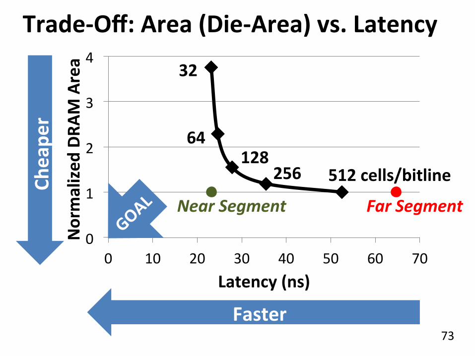
Trade-‐Off: Area (Die-‐Area) vs. Latency
0
1
2
3
4
0 10 20 30 40 50 60 70
Normalized
DRA
M Area
Latency (ns)
64
32
128 256 512 cells/bitline
Cheape
r
Faster
Near Segment Far Segment
74
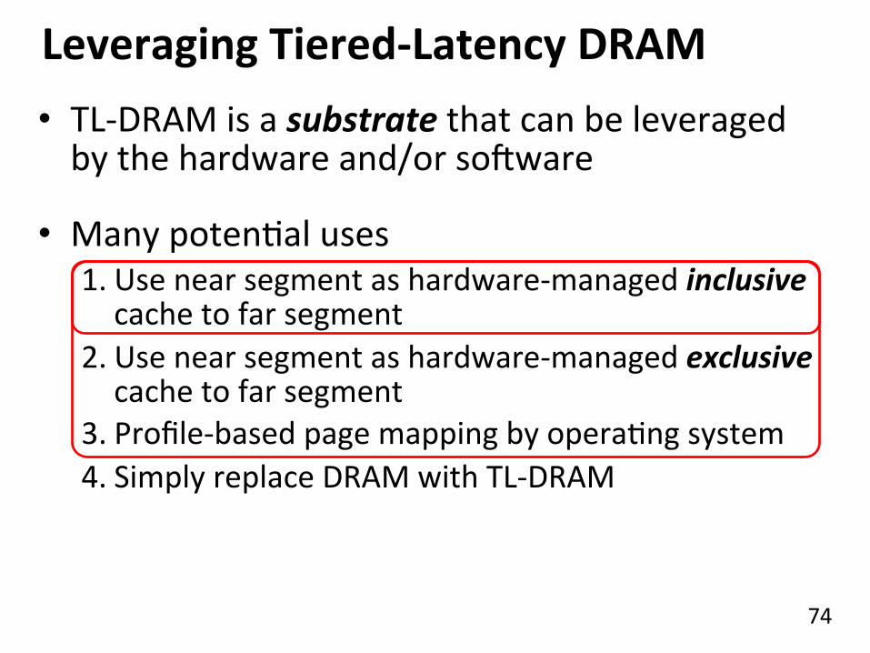
Leveraging Tiered-‐Latency DRAM • TL-‐DRAM is a substrate that can be leveraged by the hardware and/or soVware
• Many potenOal uses 1. Use near segment as hardware-‐managed inclusive cache to far segment
2. Use near segment as hardware-‐managed exclusive cache to far segment
3. Profile-‐based page mapping by operaOng system 4. Simply replace DRAM with TL-‐DRAM
75
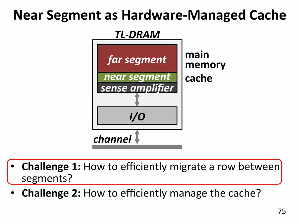
subarray
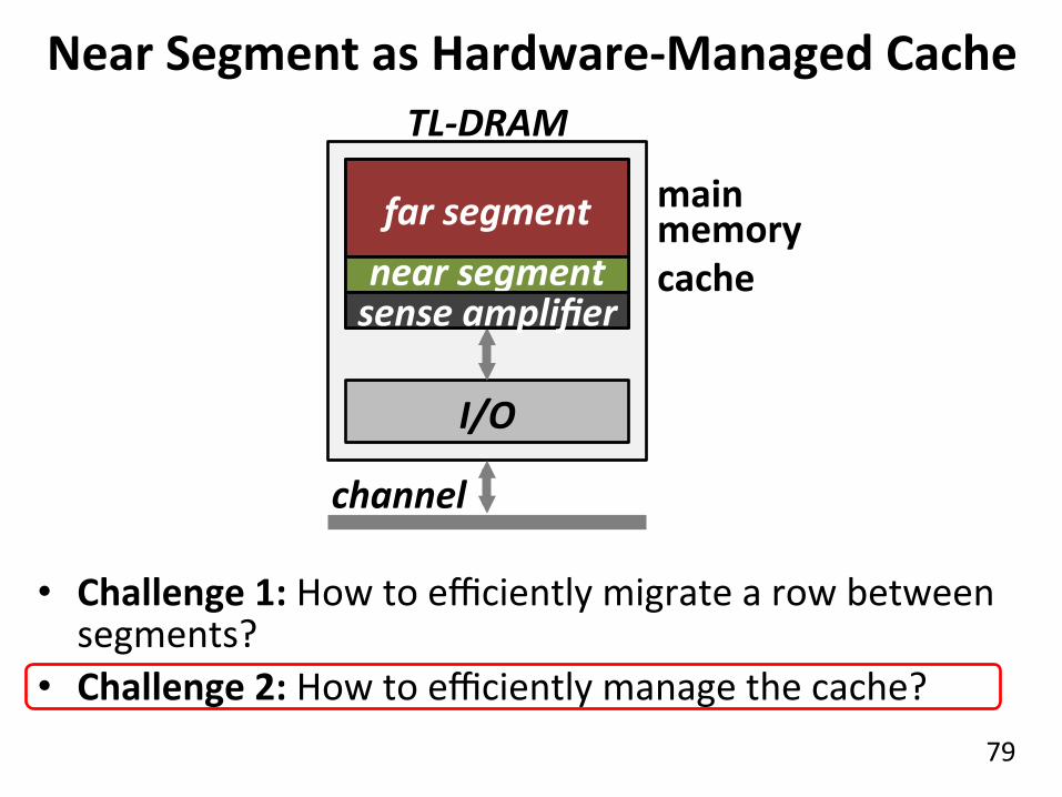
Near Segment as Hardware-‐Managed Cache TL-‐DRAM
I/O
cache
main memory
• Challenge 1: How to efficiently migrate a row between segments?
• Challenge 2: How to efficiently manage the cache?
far segment near segment sense amplifier
channel
76
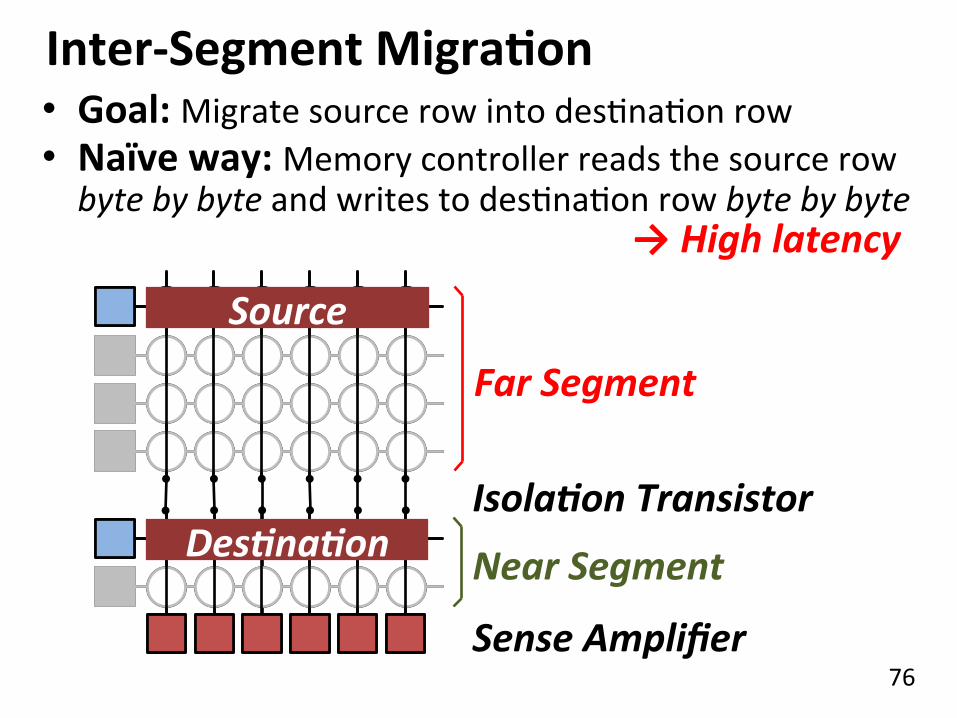
Inter-‐Segment MigraRon
Near Segment
Far Segment
IsolaJon Transistor
Sense Amplifier
Source
DesJnaJon
• Goal: Migrate source row into desOnaOon row • Naïve way: Memory controller reads the source row byte by byte and writes to desOnaOon row byte by byte
→ High latency
77
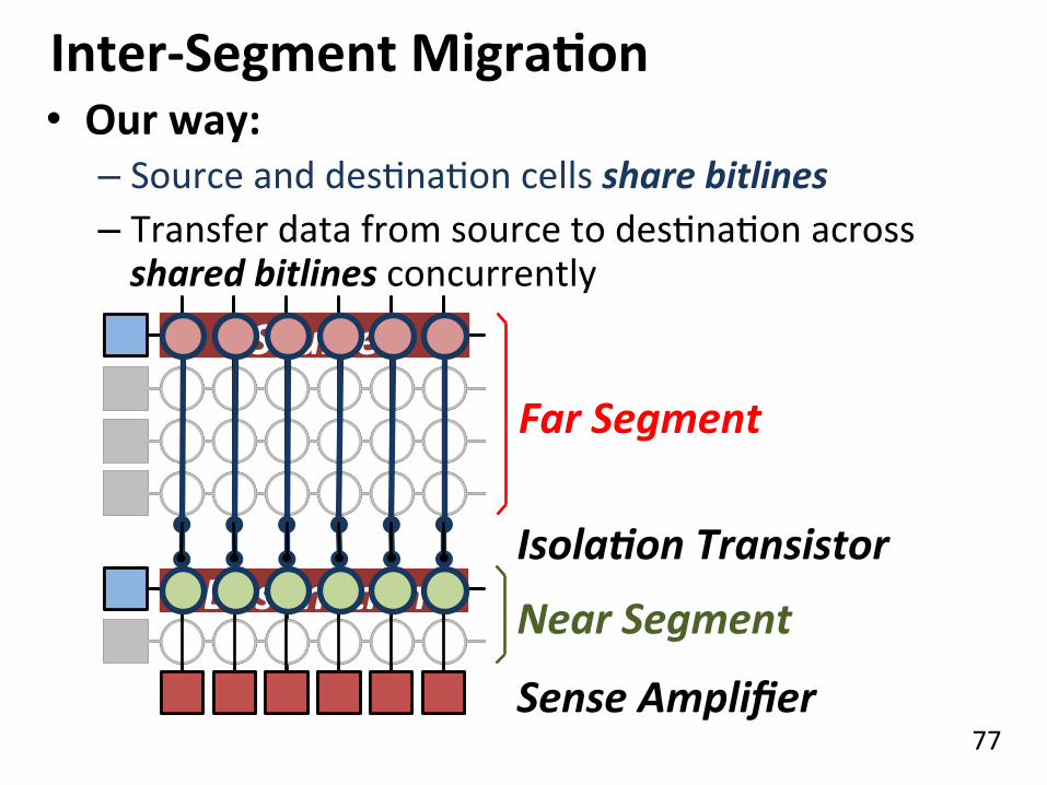
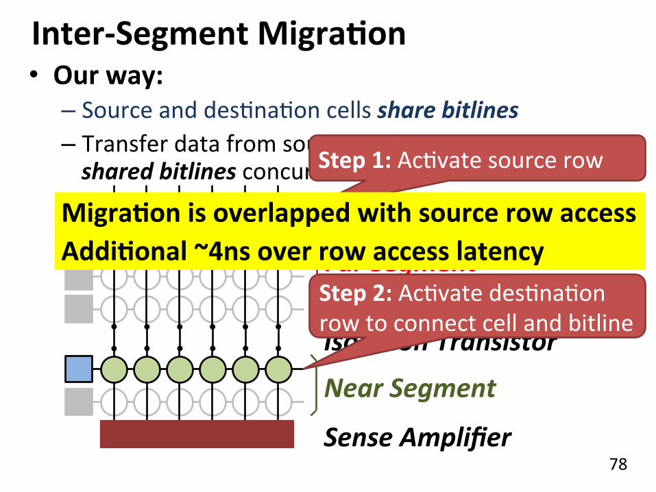
Inter-‐Segment MigraRon • Our way:
– Source and desOnaOon cells share bitlines – Transfer data from source to desOnaOon across shared bitlines concurrently
Near Segment
Far Segment
IsolaJon Transistor
Sense Amplifier
Source
DesJnaJon
78
Inter-‐Segment MigraRon
Near Segment
Far Segment
IsolaJon Transistor
Sense Amplifier
• Our way: – Source and desOnaOon cells share bitlines – Transfer data from source to desOnaOon across shared bitlines concurrently
Step 2: AcOvate desOnaOon row to connect cell and bitline
Step 1: AcOvate source row
AddiRonal ~4ns over row access latency MigraRon is overlapped with source row access
79
subarray
Near Segment as Hardware-‐Managed Cache TL-‐DRAM
I/O
cache
main memory
• Challenge 1: How to efficiently migrate a row between segments?
• Challenge 2: How to efficiently manage the cache?
far segment near segment sense amplifier
channel
80
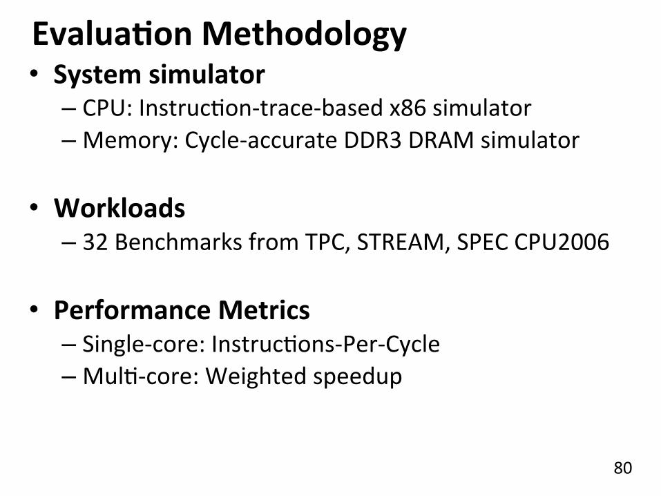
EvaluaRon Methodology • System simulator
– CPU: InstrucOon-‐trace-‐based x86 simulator – Memory: Cycle-‐accurate DDR3 DRAM simulator
• Workloads – 32 Benchmarks from TPC, STREAM, SPEC CPU2006
• Performance Metrics – Single-‐core: InstrucOons-‐Per-‐Cycle – MulO-‐core: Weighted speedup
81
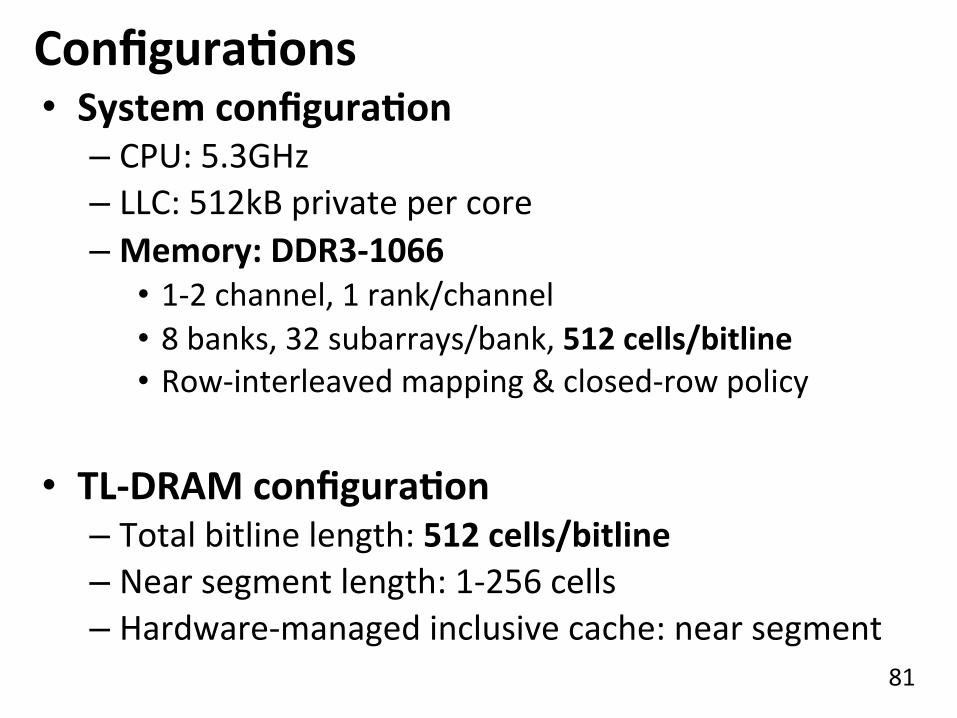
ConfiguraRons • System configuraRon
– CPU: 5.3GHz – LLC: 512kB private per core – Memory: DDR3-‐1066
• 1-‐2 channel, 1 rank/channel • 8 banks, 32 subarrays/bank, 512 cells/bitline • Row-‐interleaved mapping & closed-‐row policy
• TL-‐DRAM configuraRon – Total bitline length: 512 cells/bitline – Near segment length: 1-‐256 cells – Hardware-‐managed inclusive cache: near segment
82
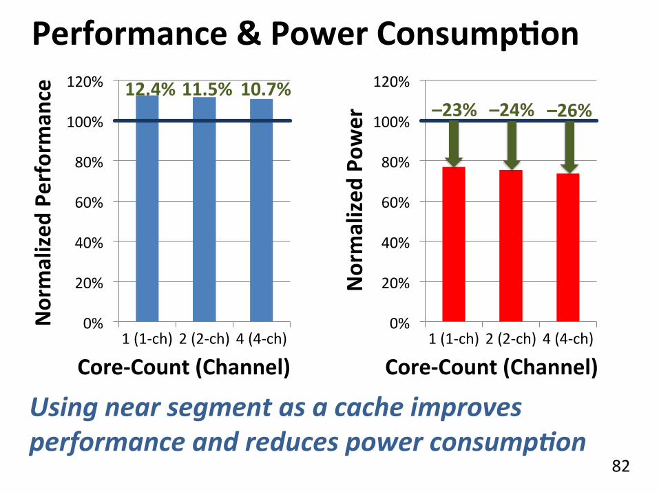
0%
20%
40%
60%
80%
100%
120%
1 (1-‐ch) 2 (2-‐ch) 4 (4-‐ch) 0%
20%
40%
60%
80%
100%
120%
1 (1-‐ch) 2 (2-‐ch) 4 (4-‐ch)
Performance & Power ConsumpRon 11.5%
Normalized
Perform
ance
Core-‐Count (Channel) Normalized
Pow
er Core-‐Count (Channel)
10.7%
12.4% –23%
–24%
–26%
Using near segment as a cache improves performance and reduces power consumpJon
83
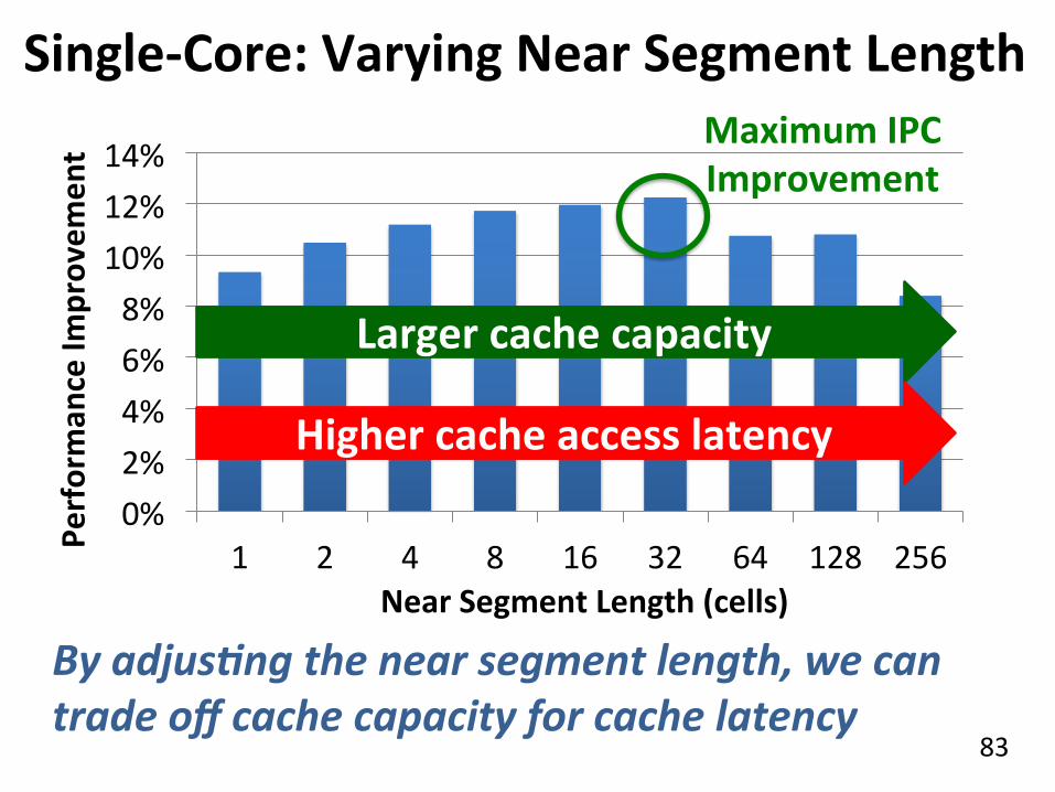
0% 2% 4% 6% 8% 10% 12% 14%
1 2 4 8 16 32 64 128 256
Single-‐Core: Varying Near Segment Length
By adjusJng the near segment length, we can trade off cache capacity for cache latency
Larger cache capacity
Higher cache access latency
Maximum IPC Improvement
Perform
ance Im
provem
ent
Near Segment Length (cells)
84
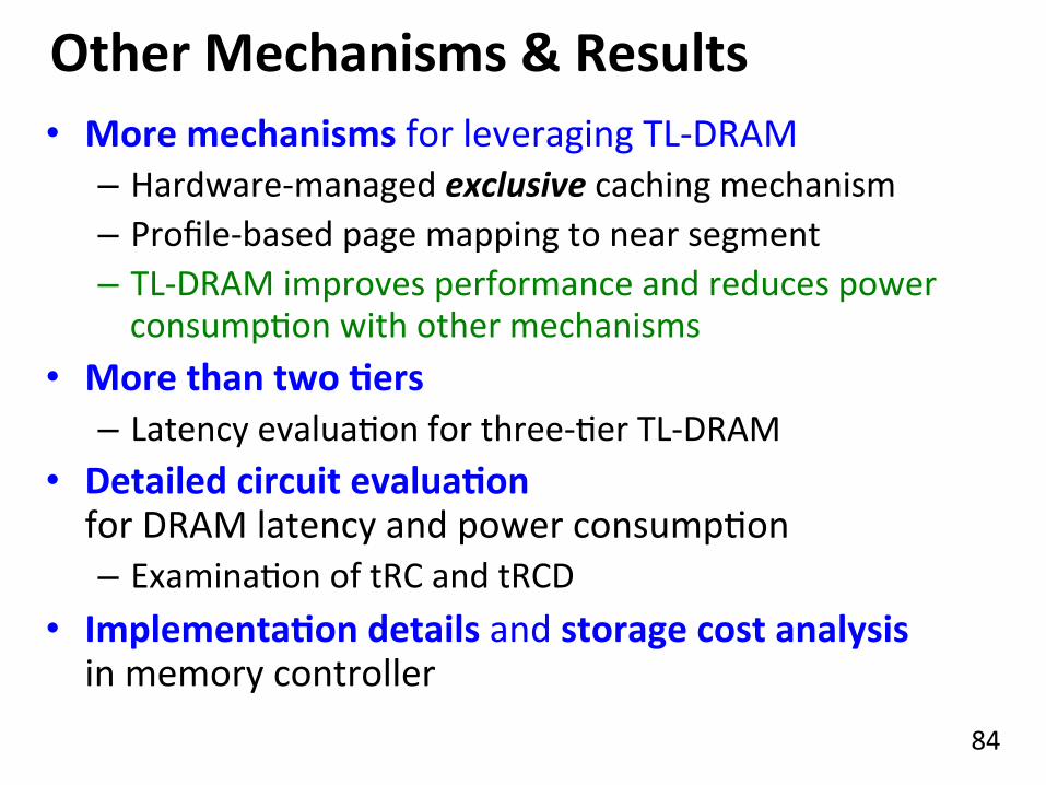
Other Mechanisms & Results • More mechanisms for leveraging TL-‐DRAM
– Hardware-‐managed exclusive caching mechanism – Profile-‐based page mapping to near segment – TL-‐DRAM improves performance and reduces power consumpOon with other mechanisms
• More than two Rers – Latency evaluaOon for three-‐Oer TL-‐DRAM
• Detailed circuit evaluaRon for DRAM latency and power consumpOon – ExaminaOon of tRC and tRCD
• ImplementaRon details and storage cost analysis in memory controller
85
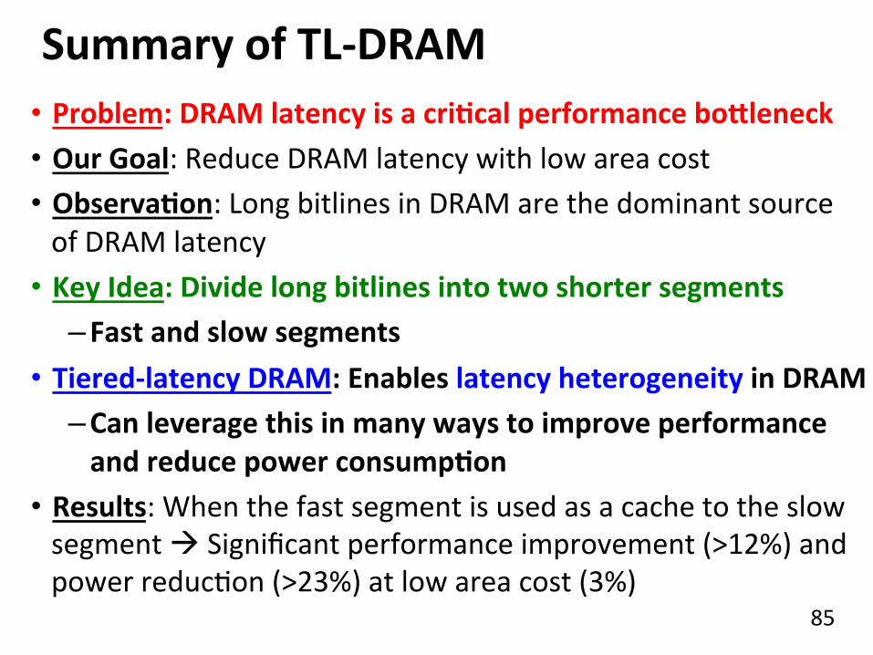
Summary of TL-‐DRAM • Problem: DRAM latency is a criRcal performance bokleneck • Our Goal: Reduce DRAM latency with low area cost • ObservaRon: Long bitlines in DRAM are the dominant source of DRAM latency
• Key Idea: Divide long bitlines into two shorter segments – Fast and slow segments
• Tiered-‐latency DRAM: Enables latency heterogeneity in DRAM – Can leverage this in many ways to improve performance and reduce power consumpRon
• Results: When the fast segment is used as a cache to the slow segment à Significant performance improvement (>12%) and power reducOon (>23%) at low area cost (3%)
New DRAM Architectures
n RAIDR: Reducing Refresh Impact n TL-DRAM: Reducing DRAM Latency n SALP: Reducing Bank Conflict Impact n RowClone: Fast Bulk Data Copy and Initialization
86
To Be Covered in Lecture 3
n Yoongu Kim, Vivek Seshadri, Donghyuk Lee, Jamie Liu, and Onur Mutlu, "A Case for Exploiting Subarray-Level Parallelism (SALP) in DRAM" Proceedings of the 39th International Symposium on Computer Architecture (ISCA), Portland, OR, June 2012. Slides (pptx)
n Vivek Seshadri, Yoongu Kim, Chris Fallin, Donghyuk Lee, Rachata Ausavarungnirun, Gennady Pekhimenko, Yixin Luo, Onur Mutlu, Phillip B. Gibbons, Michael A. Kozuch, Todd C. Mowry, "RowClone: Fast and Efficient In-DRAM Copy and Initialization of Bulk Data" CMU Computer Science Technical Report, CMU-CS-13-108, Carnegie Mellon University, April 2013.
87
Scalable Many-Core Memory Systems Lecture 2, Topic 1: DRAM Basics and
DRAM Scaling
Prof. Onur Mutlu http://www.ece.cmu.edu/~omutlu
[email protected] HiPEAC ACACES Summer School 2013
July 16, 2013


![CCPM: A Scalable and Noise-Resistant Closed Contiguous … A Scalable and Noise... · Pattern mining [2] is one of the most studied topic in the data mining literature. An ordered](https://img.pdfslide.us/doc/110x75/5f0e47627e708231d43e7847/ccpm-a-scalable-and-noise-resistant-closed-contiguous-a-scalable-and-noise.jpg)