Embed Size (px)
Citation preview
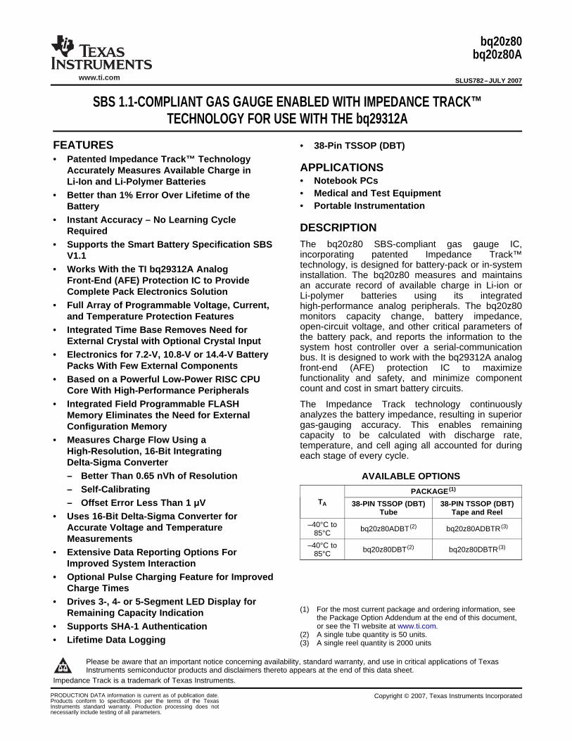
www.ti.com
FEATURES
APPLICATIONS
DESCRIPTION
bq20z80bq20z80A
SLUS782–JULY 2007
SBS 1.1-COMPLIANT GAS GAUGE ENABLED WITH IMPEDANCE TRACK™TECHNOLOGY FOR USE WITH THE bq29312A
• 38-Pin TSSOP (DBT)• Patented Impedance Track™ Technology
Accurately Measures Available Charge in• Notebook PCsLi-Ion and Li-Polymer Batteries• Medical and Test Equipment• Better than 1% Error Over Lifetime of the• Portable InstrumentationBattery
• Instant Accuracy – No Learning CycleRequired
The bq20z80 SBS-compliant gas gauge IC,• Supports the Smart Battery Specification SBSincorporating patented Impedance Track™V1.1technology, is designed for battery-pack or in-system• Works With the TI bq29312A Analoginstallation. The bq20z80 measures and maintainsFront-End (AFE) Protection IC to Provide an accurate record of available charge in Li-ion or
Complete Pack Electronics Solution Li-polymer batteries using its integrated• Full Array of Programmable Voltage, Current, high-performance analog peripherals. The bq20z80
monitors capacity change, battery impedance,and Temperature Protection Featuresopen-circuit voltage, and other critical parameters of• Integrated Time Base Removes Need forthe battery pack, and reports the information to theExternal Crystal with Optional Crystal Inputsystem host controller over a serial-communication
• Electronics for 7.2-V, 10.8-V or 14.4-V Battery bus. It is designed to work with the bq29312A analogPacks With Few External Components front-end (AFE) protection IC to maximize
functionality and safety, and minimize component• Based on a Powerful Low-Power RISC CPUcount and cost in smart battery circuits.Core With High-Performance Peripherals
• Integrated Field Programmable FLASH The Impedance Track technology continuouslyanalyzes the battery impedance, resulting in superiorMemory Eliminates the Need for Externalgas-gauging accuracy. This enables remainingConfiguration Memorycapacity to be calculated with discharge rate,• Measures Charge Flow Using atemperature, and cell aging all accounted for during
High-Resolution, 16-Bit Integrating each stage of every cycle.Delta-Sigma Converter– Better Than 0.65 nVh of Resolution AVAILABLE OPTIONS– Self-Calibrating PACKAGE (1)
TA– Offset Error Less Than 1 μV 38-PIN TSSOP (DBT) 38-PIN TSSOP (DBT)Tube Tape and Reel• Uses 16-Bit Delta-Sigma Converter for
–40°C toAccurate Voltage and Temperature bq20z80ADBT (2) bq20z80ADBTR (3)85°C
Measurements–40°C to bq20z80DBT (2) bq20z80DBTR (3)
• Extensive Data Reporting Options For 85°CImproved System Interaction
• Optional Pulse Charging Feature for ImprovedCharge Times
• Drives 3-, 4- or 5-Segment LED Display for(1) For the most current package and ordering information, seeRemaining Capacity Indication the Package Option Addendum at the end of this document,
or see the TI website at www.ti.com.• Supports SHA-1 Authentication(2) A single tube quantity is 50 units.• Lifetime Data Logging (3) A single reel quantity is 2000 units
Please be aware that an important notice concerning availability, standard warranty, and use in critical applications of TexasInstruments semiconductor products and disclaimers thereto appears at the end of this data sheet.
Impedance Track is a trademark of Texas Instruments.
PRODUCTION DATA information is current as of publication date. Copyright © 2007, Texas Instruments IncorporatedProducts conform to specifications per the terms of the TexasInstruments standard warranty. Production processing does notnecessarily include testing of all parameters.
www.ti.com
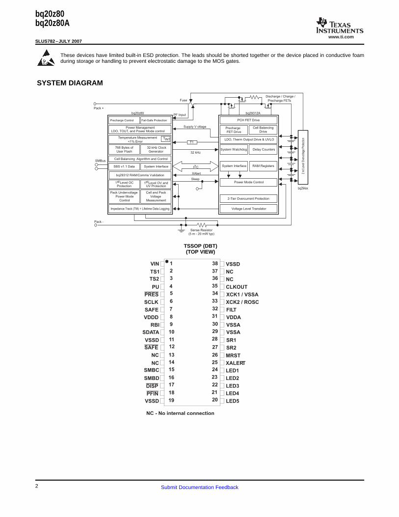
SYSTEM DIAGRAM
LDO, Therm Output Drive & UVLO
Power ManagementLDO, TOUT, and Power Mode control
I2C
Impedance Track (TM) + Lifetime Data Logging
SMBus
Pack +
Pack -
Discharge / Charge /
Precharge FETs
Cell and Pack
Voltage
Measurement
Precharge
FET Drive
2-Tier Overcurrent Protection
32-kHz Clock
Generator
bq20z80
768 Bytes of
User Flash
Fuse
1stLevel OV andUV Protection
Pack Undervoltage
Power Mode
Control
Precharge Control
Delay Counters
Cell Balancing Algorithm and Control
Cell Balancing
Drive
System Interface
System Watchdog
Voltage Level Translator
System Interface
32 kHz
Power Mode Control
Fail-Safe Protection
T1
1stLevel OCProtection
Temperature Measurement
<1% ErrorTINT
Supply V oltage
bq29312A
PCH FET Drive
RAM RegistersSBS v1.1 Data
bq29312 RAM/Comms Validation
2 nd
Lev
el O
verv
olta
ge P
rote
ctio
n
bq294xx
XAlert
Sleep
Sense Resistor(5 m - 20 mW typ)
PF Input
1
2
7
6
5
4
3
38
37
36
35
34
33
32
VIN
TS1
TS2
PU
PRES
SCLK
VSSD
NC
NC
CLKOUT
XCK1 / VSSA
XCK2 / ROSC
FILTSAFE
VDDD VDDA
RBI
SDATA
VSSD
SAFE SR2
SR1
VSSA
VSSA
8
9
10
11
12
31
30
29
28
27
13
14
19
18
17
16
15
26
25
24
23
22
21
20
NC
NC
SMBC
SMBD
DISP
PFIN
MRST
XALERT
LED1
LED2
LED3
LED4
LED5VSSD
NC - No internal connection
bq20z80bq20z80A
SLUS782–JULY 2007
These devices have limited built-in ESD protection. The leads should be shorted together or the device placed in conductive foamduring storage or handling to prevent electrostatic damage to the MOS gates.
TSSOP (DBT)(TOP VIEW)
2 Submit Documentation Feedback
www.ti.com
bq20z80bq20z80A
SLUS782–JULY 2007
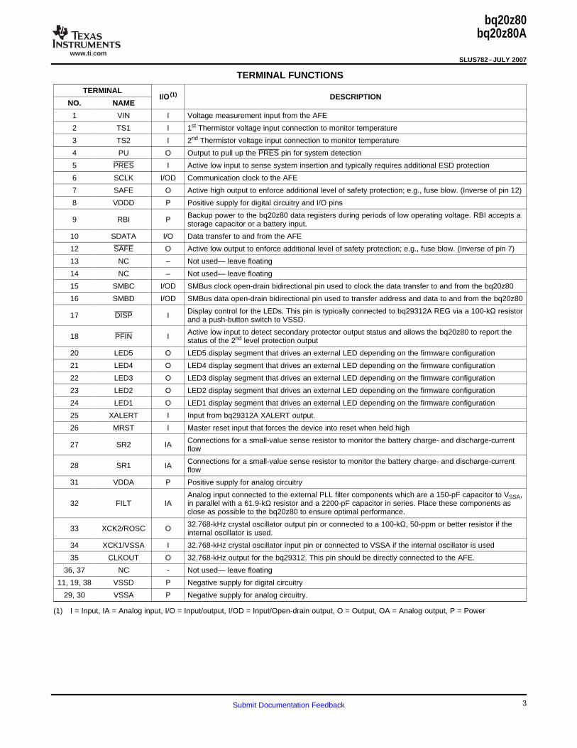
TERMINAL FUNCTIONS
TERMINALI/O (1) DESCRIPTION
NO. NAME
1 VIN I Voltage measurement input from the AFE
2 TS1 I 1st Thermistor voltage input connection to monitor temperature
3 TS2 I 2nd Thermistor voltage input connection to monitor temperature
4 PU O Output to pull up the PRES pin for system detection
5 PRES I Active low input to sense system insertion and typically requires additional ESD protection
6 SCLK I/OD Communication clock to the AFE
7 SAFE O Active high output to enforce additional level of safety protection; e.g., fuse blow. (Inverse of pin 12)
8 VDDD P Positive supply for digital circuitry and I/O pins
Backup power to the bq20z80 data registers during periods of low operating voltage. RBI accepts a9 RBI P storage capacitor or a battery input.
10 SDATA I/O Data transfer to and from the AFE
12 SAFE O Active low output to enforce additional level of safety protection; e.g., fuse blow. (Inverse of pin 7)
13 NC – Not used— leave floating
14 NC – Not used— leave floating
15 SMBC I/OD SMBus clock open-drain bidirectional pin used to clock the data transfer to and from the bq20z80
16 SMBD I/OD SMBus data open-drain bidirectional pin used to transfer address and data to and from the bq20z80
Display control for the LEDs. This pin is typically connected to bq29312A REG via a 100-kΩ resistor17 DISP I and a push-button switch to VSSD.
Active low input to detect secondary protector output status and allows the bq20z80 to report the18 PFIN I status of the 2nd level protection output
20 LED5 O LED5 display segment that drives an external LED depending on the firmware configuration
21 LED4 O LED4 display segment that drives an external LED depending on the firmware configuration
22 LED3 O LED3 display segment that drives an external LED depending on the firmware configuration
23 LED2 O LED2 display segment that drives an external LED depending on the firmware configuration
24 LED1 O LED1 display segment that drives an external LED depending on the firmware configuration
25 XALERT I Input from bq29312A XALERT output.
26 MRST I Master reset input that forces the device into reset when held high
Connections for a small-value sense resistor to monitor the battery charge- and discharge-current27 SR2 IA flow
Connections for a small-value sense resistor to monitor the battery charge- and discharge-current28 SR1 IA flow
31 VDDA P Positive supply for analog circuitry
Analog input connected to the external PLL filter components which are a 150-pF capacitor to VSSA,32 FILT IA in parallel with a 61.9-kΩ resistor and a 2200-pF capacitor in series. Place these components as
close as possible to the bq20z80 to ensure optimal performance.
32.768-kHz crystal oscillator output pin or connected to a 100-kΩ, 50-ppm or better resistor if the33 XCK2/ROSC O internal oscillator is used.
34 XCK1/VSSA I 32.768-kHz crystal oscillator input pin or connected to VSSA if the internal oscillator is used
35 CLKOUT O 32.768-kHz output for the bq29312. This pin should be directly connected to the AFE.
36, 37 NC - Not used— leave floating
11, 19, 38 VSSD P Negative supply for digital circuitry
29, 30 VSSA P Negative supply for analog circuitry.
(1) I = Input, IA = Analog input, I/O = Input/output, I/OD = Input/Open-drain output, O = Output, OA = Analog output, P = Power
3Submit Documentation Feedback
www.ti.com
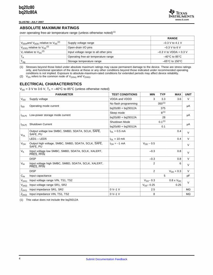
ABSOLUTE MAXIMUM RATINGS
ELECTRICAL CHARACTERISTICS
bq20z80bq20z80A
SLUS782–JULY 2007
over operating free-air temperature range (unless otherwise noted) (1)
RANGE
VDDAand VDDD relative to VSS(2) Supply voltage range –0.3 V to 4.1 V
V(IOD) relative to VSS(2) Open-drain I/O pins –0.3 V to 6 V
VI relative to VSS(2) Input voltage range to all other pins –0.3 V to VDDA + 0.3 V
TA Operating free-air temperature range –40°C to 85°C
Tstg Storage temperature range –65°C to 150°C
(1) Stresses beyond those listed under absolute maximum ratings may cause permanent damage to the device. These are stress ratingsonly, and functional operation of the device at these or any other conditions beyond those indicated under recommended operatingconditions is not implied. Exposure to absolute-maximum-rated conditions for extended periods may affect device reliability.
(2) VSS refers to the common node of V(SSA) and V(SSD).
VDD = 3 V to 3.6 V, TA = –40°C to 85°C (unless otherwise noted)
PARAMETER TEST CONDITIONS MIN TYP MAX UNIT
VDD Supply voltage VDDA and VDDD 3 3.3 3.6 V
No flash programming 350 (1)
IDD Operating mode current μAbq20z80 + bq29312A 375
Sleep mode 8 (1)
I(SLP) Low-power storage mode current μAbq20z80 + bq29312A 28
Shutdown Mode 0.1 (1)
I(SLP) Shutdown Current μAbq20z80 + bq29312A 0.1
Output voltage low SMBC, SMBD, SDATA, SCLK, SAFE, IOL = 0.5 mA 0.4 VSAFE, PUVOL
LED1 – LED5 IOL = 10 mA 0.4 V
VOH Output high voltage, SMBC, SMBD, SDATA, SCLK, SAFE, IOH = –1 mA VDD – 0.5 VSAFE, PU
VIL Input voltage low SMBC, SMBD, SDATA, SCLK, XALERT, –0.3 0.8 VPRES, PFIN
DISP –0.3 0.8 V
VIH Input voltage high SMBC, SMBD, SDATA, SCLK, XALERT, 2 6 VPRES, PFIN
DISP 2 VDD + 0.3 V
CIN Input capacitance 5 pF
V(AI1) Input voltage range VIN, TS1, TS2 VSS– 0.3 0.8 x VDDV
V(AI2) Input voltage range SR1, SR2 VSS– 0.25 0.25
Z(AI1) Input impedance SR1, SR2 0 V–1 V 2.5 MΩ
Z(AI2) Input impedance VIN, TS1, TS2 0 V–1 V 8 MΩ
(1) This value does not include the bq29312A
4 Submit Documentation Feedback
www.ti.com
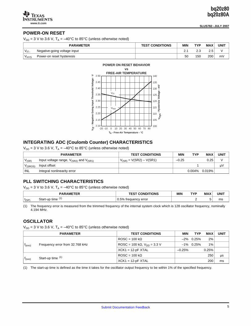
POWER-ON RESET
2.10
2.15
2.20
2.25
2.30
2.35
2.40
2.45
2.50
-20 -10 0 10 20 30 40 50 60 70 80100
105
110
115
120
125
130
135
140
TA - Free-Air Temperature - °C
- N
egat
ive
Go
ing
Inp
ut
Th
resh
old
Vo
ltag
e -
V
POWER ON RESET BEHAVIORvs
FREE-AIR TEMPERATURE
VIT
VIT-
Vhys
Vh
ys-
Hys
teri
sis
Volt
age
- m
V
INTEGRATING ADC (Coulomb Counter) CHARACTERISTICS
PLL SWITCHING CHARACTERISTICS
OSCILLATOR
bq20z80bq20z80A
SLUS782–JULY 2007
VDD = 3 V to 3.6 V, TA = –40°C to 85°C (unless otherwise noted)
PARAMETER TEST CONDITIONS MIN TYP MAX UNIT
VIT– Negative-going voltage input 2.1 2.3 2.5 V
VHYS Power-on reset hysteresis 50 150 200 mV
VDD = 3 V to 3.6 V, TA = –40°C to 85°C (unless otherwise noted)
PARAMETER TEST CONDITIONS MIN TYP MAX UNIT
V(SR) Input voltage range, V(SR2) and V(SR1) V(SR) = V(SR2) – V(SR1) –0.25 0.25 V
V(SROS) Input offset 1 μV
INL Integral nonlinearity error 0.004% 0.019%
VDD = 3 V to 3.6 V, TA = –40°C to 85°C (unless otherwise noted)
PARAMETER TEST CONDITIONS MIN TYP MAX UNIT
t(SP) Start-up time (1) 0.5% frequency error 2 5 ms
(1) The frequency error is measured from the trimmed frequency of the internal system clock which is 128 oscillator frequency, nominally4.194 MHz.
VDD = 3 V to 3.6 V, TA = –40°C to 85°C (unless otherwise noted)
PARAMETER TEST CONDITIONS MIN TYP MAX UNIT
ROSC = 100 kΩ –2% 0.25% 2%
f(exo) Frequency error from 32.768 kHz ROSC = 100 kΩ, VDD = 3.3 V –1% 0.25% 1%
XCK1 = 12-pF XTAL –0.25% 0.25%
ROSC = 100 kΩ 250 μsf(sxo) Start-up time (1)
XCK1 = 12-pF XTAL 200 ms
(1) The start-up time is defined as the time it takes for the oscillator output frequency to be within 1% of the specified frequency.
5Submit Documentation Feedback
www.ti.com
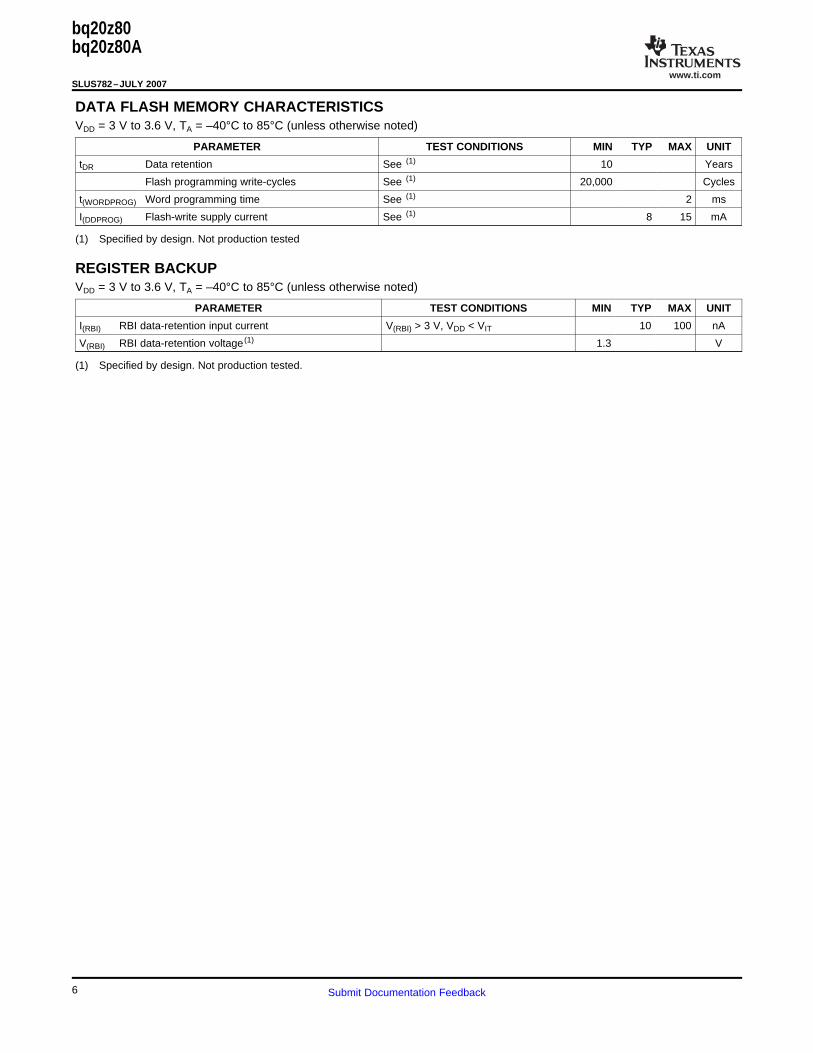
DATA FLASH MEMORY CHARACTERISTICS
REGISTER BACKUP
bq20z80bq20z80A
SLUS782–JULY 2007
VDD = 3 V to 3.6 V, TA = –40°C to 85°C (unless otherwise noted)
PARAMETER TEST CONDITIONS MIN TYP MAX UNIT
tDR Data retention See (1) 10 Years
Flash programming write-cycles See (1) 20,000 Cycles
t(WORDPROG) Word programming time See (1) 2 ms
I(DDPROG) Flash-write supply current See (1) 8 15 mA
(1) Specified by design. Not production tested
VDD = 3 V to 3.6 V, TA = –40°C to 85°C (unless otherwise noted)
PARAMETER TEST CONDITIONS MIN TYP MAX UNIT
I(RBI) RBI data-retention input current V(RBI) > 3 V, VDD < VIT 10 100 nA
V(RBI) RBI data-retention voltage (1) 1.3 V
(1) Specified by design. Not production tested.
6 Submit Documentation Feedback
www.ti.com
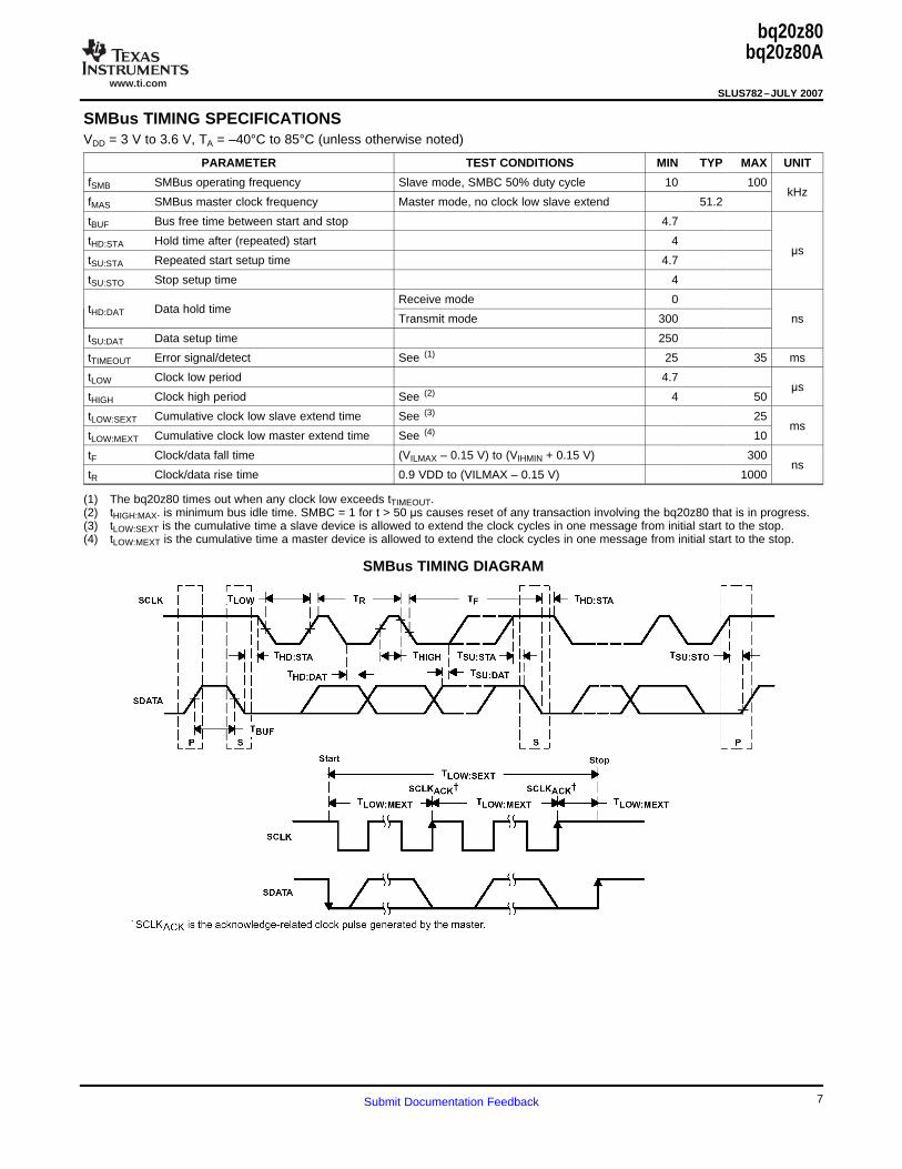
SMBus TIMING SPECIFICATIONS
bq20z80bq20z80A
SLUS782–JULY 2007
VDD = 3 V to 3.6 V, TA = –40°C to 85°C (unless otherwise noted)
PARAMETER TEST CONDITIONS MIN TYP MAX UNIT
fSMB SMBus operating frequency Slave mode, SMBC 50% duty cycle 10 100kHz
fMAS SMBus master clock frequency Master mode, no clock low slave extend 51.2
tBUF Bus free time between start and stop 4.7
tHD:STA Hold time after (repeated) start 4μs
tSU:STA Repeated start setup time 4.7
tSU:STO Stop setup time 4
Receive mode 0tHD:DAT Data hold time
Transmit mode 300 ns
tSU:DAT Data setup time 250
tTIMEOUT Error signal/detect See (1) 25 35 ms
tLOW Clock low period 4.7μs
tHIGH Clock high period See (2) 4 50
tLOW:SEXT Cumulative clock low slave extend time See (3) 25ms
tLOW:MEXT Cumulative clock low master extend time See (4) 10
tF Clock/data fall time (VILMAX – 0.15 V) to (VIHMIN + 0.15 V) 300ns
tR Clock/data rise time 0.9 VDD to (VILMAX – 0.15 V) 1000
(1) The bq20z80 times out when any clock low exceeds tTIMEOUT.(2) tHIGH:MAX. is minimum bus idle time. SMBC = 1 for t > 50 μs causes reset of any transaction involving the bq20z80 that is in progress.(3) tLOW:SEXT is the cumulative time a slave device is allowed to extend the clock cycles in one message from initial start to the stop.(4) tLOW:MEXT is the cumulative time a master device is allowed to extend the clock cycles in one message from initial start to the stop.
SMBus TIMING DIAGRAM
7Submit Documentation Feedback
www.ti.com
FEATURE SET
Primary (1st Level) Safety Features
Secondary (2nd Level) Safety Features
Charge Control Features
bq20z80bq20z80A
SLUS782–JULY 2007
NOTE
The bq20z80-V102 is designed to work with the bq29312A AFE. The bq20z80features are only available with the bq29312A.
.
The bq20z80 supports a wide range of battery and system protection features that care easily configured. Theprimary safety features includes:
• Battery cell over/undervoltage protection• Battery pack over/undervoltage protection• 2 independent charge overcurrent protection• 3 independent discharge overcurrent protection• Short circuit protection• Overtemperature protection• Host watchdog
The secondary safety features of the bq20z80 can be used to indicate more serious faults via the SAFE (pin 7)and SAFE (pin 12) pins. These pins can be used to blow a in-line fuse to permanently disable the battery packfrom charging or discharging. The secondary safety features includes:
• Safety over voltage• Battery cell imbalance• 2nd level protection IC input• Safety overcurrent• Safety overtemperature• Open thermistor• Charge FET and 0 Volt Charge FET fault• Discharge FET fault• Fuse blow failure detection• AFE communication error• Internal flash data error
The bq20z80 charge control features includes:
• Report the appropriate charging current needed for constant current charging and the appropriate chargingvoltage needed for constant voltage charging to a smart charger using SMBus broadcasts.
• Determines the chemical state of charge of each battery cell using Impedance Track™ and can reduce thecharge difference of the battery cells in fully charged state of the battery pack gradually using cell balancingalgorithm during charging. This prevents fully charged cells from overcharging causing excessive degradationand also increases the usable pack energy by preventing to early charge termination
• supports pre-charging/zero-volt charging• support fast charging• supports pulse charging• detects charge termination• report charging faults and also indicate charge status via charge and discharge alarms.
8 Submit Documentation Feedback
www.ti.com
Gas Gauging
LED Display
LifeTime Data Logging Features
Authentication
Power Modes
CONFIGURATION
Oscillator Function
bq20z80bq20z80A
SLUS782–JULY 2007
FEATURE SET (continued)
The bq20z80 uses the Impedance Track™ Technology to measure and calculate the available charge in batterycells. The achievable accuracy is better than the coulomb counting method over the lifetime of the battery andthere is no full charge discharge learning cycle required.
See Theory and Implementation of Impedance Track Battery Fuel-Gauging Algorithm application note(SLUA364) for further details.
The bq20z80 can drive 3-, 4-, or 5- segment LED display for remaining capacity indication.
The bq20z80 offers a lifetime data logging array, where all important measurements are stored for warranty andanalysis purposes. The data monitored includes:
• Lifetime maximum temperature• Lifetime minimum temperature• Lifetime maximum battery cell voltage• Lifetime minimum battery cell voltage• Lifetime maximum battery pack voltage• Lifetime minimum battery pack voltage• Lifetime maximum charge current• Lifetime maximum discharge current• Lifetime maximum charge power• Lifetime maximum discharge power• Lifetime maximum average discharge current• Lifetime maximum average discharge power• Lifetime average temperature
The bq20z80 supports authentication by the host using SHA-1.
The bq20z80 supports 3 different power modes to reduce power consumption:
• In Normal Mode, the bq20z80 performs measurements, calculations, protection decision, data update in 1second intervals. Between these intervals, the bq20z80 is in a reduced power stage.
• In Sleep Mode, the bq20z80 performs measurements, calculations, protection decision, data update inadjustable time intervals. Between these intervals, the bq20z80 is in a reduced power stage.
• In Shutdown Mode the bq20z80 is completely disabled.
The oscillator of the bq20z80 can be set up for internal or external operation. On power up, the bq20z80automatically attempts to start the internal oscillator. If a 100-kΩ resistor is not connected to ROSC (pin 33),then it attempts to start the oscillator using an external 32.768-kHz crystal.
NOTE
Install either the 100-kΩ ROSC resistor or the 12-pF, 32.768-kHz crystal. Do notinstall both.
9Submit Documentation Feedback

www.ti.com
System Present Operation
BATTERY PARAMETER MEASUREMENTS
Charge and Discharge Counting
Voltage
Current
Auto Calibration
Temperature
COMMUNICATIONS
SMBus On and Off State
bq20z80bq20z80A
SLUS782–JULY 2007
FEATURE SET (continued)
The performance of the internal oscillator depends on the tolerance of the 100-kΩ resistor between RSOC (pin33) and VSSA (pin 34). Choose a resistor with a tolerance of ±0.1%, and 50-ppm or better temperature drift.Place this resistor as close as possible to the bq20z80. If a 12-pF crystal is used, place it as close as possible tothe XCK1 (pin 34) and XCK2 (pin 33) pins. If not properly implemented, the PCB layout in this area can degradeoscillator performance.
The bq20z80 pulls the PU pin high periodically (1 s). Connect this pin to the PRES pin of the bq20z80 via aresistor of approximately 5 kΩ. The bq20z80 measures the PRES input during the PU-active period to determineits state. If PRES input is pulled to ground by external system, the bq20z80 detects this as system present.
The bq20z80 uses an integrating delta-sigma analog-to-digital converter (ADC) for current measurement, and asecond delta-sigma ADC for individual cell and battery voltage, and temperature measurement.
The integrating delta-sigma ADC measures the charge/discharge flow of the battery by measuring the voltagedrop across a small-value sense resistor between the SR1 and SR2 pins. The integrating ADC measures bipolarsignals from -0.25 V to 0.25 V. The bq20z80 detects charge activity when VSR = V(SR1)-V(SR2)is positive anddischarge activity when VSR = V(SR1)-V(SR2) is negative. The bq20z80 continuously integrates the signal overtime, using an internal counter. The fundamental rate of the counter is 0.65 nVh.
The bq20z80 updates the individual series cell voltages through the bq29312A at one second intervals. Thebq20z80 configures the bq29312A to connect the selected cell, cell offset, or bq29312A VREF to the CELL pinof the bq29312A, which is required to be connected to VIN of the bq20z80. The internal ADC of the bq20z80measures the voltage, scales and calibrates it appropriately. This data is also used to calculate the impedanceof the cell for the Impedance Track™ gas-gauging.
The bq20z80 uses the SR1 and SR2 inputs to measure and calculate the battery charge and discharge currentusing a 5 mΩ to 20 mΩ (typical) sense resistor.
The bq20z80 provides an auto-calibration feature to cancel the voltage offset error across SR1 and SR2 formaximum charge measurement accuracy. The bq20z80 performs auto-calibration when the SMBus lines staylow continuously for a minimum of 5 s.
The bq20z80 TS1 and TS2 inputs, in conjunction with two identical NTC thermistors (default are Semitec103AT), measure the battery environmental temperature. The bq20z80 can also be configured to use its internaltemperature sensor.
The bq20z80 uses SMBus v1.1 with Master Mode and package error checking (PEC) options per the SBSspecification.
The bq20z80 detects an SMBus off state when SMBC and SMBD are logic-low greater than an adjustableperiod of time. Clearing this state requires either SMBC or SMBD to transition high. Within 1 ms, thecommunication bus is available.
10 Submit Documentation Feedback
www.ti.com
SBS Commands
bq20z80bq20z80A
SLUS782–JULY 2007
FEATURE SET (continued)
Table 1. SBS COMMANDS
SBS Cmd Mode Name Format Size in Min Max Default Value UnitBytes Value Value
0x00 R/W ManufacturerAccess hex 2 0x0000 0xffff —
0x01 R/W RemainingCapacityAlarm unsigned int 2 0 65535 — mAh or10mWh
0x02 R/W RemainingTimeAlarm unsigned int 2 0 65535 — min
0x03 R/W BatteryMode hex 2 0x0000 0xffff —
0x04 R/W AtRate signed int 2 –32768 32767 — mA or 10mW
0x05 R AtRateTimeToFull unsigned int 2 0 65535 — min
0x06 R AtRateTimeToEmpty unsigned int 2 0 65535 — min
0x07 R AtRateOK unsigned int 2 0 65535 —
0x08 R Temperature unsigned int 2 0 65535 — 0.1°K
0x09 R Voltage unsigned int 2 0 20000 — mV
0x0a R Current signed int 2 –32768 32767 — mA
0x0b R AverageCurrent signed int 2 –32768 32767 — mA
0x0c R MaxError unsigned int 1 0 100 — %
0x0d R RelativeStateOfCharge unsigned int 1 0 100 — %
0x0e R AbsoluteStateOfCharge unsigned int 1 0 100 — %
0x0f R RemainingCapacity unsigned int 2 0 65535 — mAh or10mWh
0x10 R FullChargeCapacity unsigned int 2 0 65535 — mAh or10mWh
0x11 R RunTimeToEmpty unsigned int 2 0 65535 — min
0x12 R AverageTimeToEmpty unsigned int 2 0 65535 — min
0x13 R AverageTimeToFull unsigned int 2 0 65535 — min
0x14 R ChargingCurrent unsigned int 2 0 65535 — mA
0x15 R ChargingVoltage unsigned int 2 0 65535 — mV
0x16 R BatteryStatus unsigned int 2 0x0000 0xffff —
0x17 R/W CycleCount unsigned int 2 0 65535 —
0x18 R/W DesignCapacity unsigned int 2 0 65535 mAh or10mWh
0x19 R/W DesignVoltage unsigned int 2 7000 16000 14400 mV
0x1a R/W SpecificationInfo unsigned int 2 0x0000 0xffff 0x0031
0x1b R/W ManufactureDate unsigned int 2 0 65535 0
0x1c R/W SerialNumber hex 2 0x0000 0xffff 0x0001
0x20 R/W ManufacturerName String 11+1 — — Texas Instruments ASCII
0x21 R/W DeviceName String 7+1 — — bq20z80 ASCII
0x22 R/W DeviceChemistry String 4+1 — — LION ASCII
0x23 R ManufacturerData String 14+1 — — — ASCII
0x2f R/W Authenticate String 20+1 — — — ASCII
0x3c R CellVoltage4 unsigned int 2 0 65535 mV
0x3d R CellVoltage3 unsigned int 2 0 65535 mV
0x3e R CellVoltage2 unsigned int 2 0 65535 mV
0x3f R CellVoltage1 unsigned int 2 0 65535 mV
11Submit Documentation Feedback
www.ti.com
Firmware Version Changes
bq20z80-V102 to bq20z80-V110 Changes
bq20z80bq20z80A
SLUS782–JULY 2007
Table 2. EXTENDED SBS COMMANDS
SBS Mode Name Format Size in Min Value Max Value Default Value UnitCmd Bytes
0x45 R AFEData String 11+1 — — — ASCII
0x46 R/W FETControl hex 1 0x00 0xff —
0x4f R StateOfHealth unsigned int 1 0 100 — %
0x50 R SafetyAlert hex 2 0x0000 0xffff —
0x51 R SafetyStatus hex 2 0x0000 0xffff —
0x52 R PFAlert hex 2 0x0000 0xffff —
0x53 R PFStatus hex 2 0x0000 0xffff —
0x54 R OperationStatus hex 2 0x0000 0xffff —
0x55 R ChargingStatus hex 2 0x0000 0xffff —
0x57 R ResetData hex 2 0x0000 0xffff —
0x58 R WDResetData unsigned int 2 0 65535 —
0x5a R PackVoltage unsigned int 2 0 65535 — mV
0x5d R AverageVoltage unsigned int 2 0 65535 mV
0x60 R/W UnSealKey hex 4 0x00000000 0xffffffff —
0x62 R/W PFKey hex 4 0x00000000 0xffffffff —
0x63 R/W AuthenKey3 hex 4 0x00000000 0xffffffff —
0x64 R/W AuthenKey2 hex 4 0x00000000 0xffffffff —
0x65 R/W AuthenKey1 hex 4 0x00000000 0xffffffff —
0x66 R/W AuthenKey0 hex 4 0x00000000 0xffffffff —
0x70 R/W ManufacturerInfo String 8+1 — — —
0x71 R/W SenseResistor unsigned int 2 0 65535 — μΩ0x77 R/W DataflashClass hex 2 0x0000 0xffff —
0x78 R/W DataFlashSubClass1 hex 32 — — —
0x79 R/W DataFlashSubClass2 hex 32 — — —
0x7a R/W DataFlashSubClass3 hex 32 — — —
0x7b R/W DataFlashSubClass4 hex 32 — — —
0x7c R/W DataFlashSubClass5 hex 32 — — —
0x7d R/W DataFlashSubClass6 hex 32 — — —
0x7e R/W DataFlashSubClass7 hex 32 — — —
0x7f R/W DataFlashSubClass8 hex 32 — — —
Table 3. CHANGE DETAILS
CHANGE bq0z80-V110 bq20z80-V102 COMMENTS
Allows alarm based on DF.Remaining Energy Alarm Feature not available make bq20z80 compatible toremaining battery energy added bq20z90
Permanent fail fuse blow can [PRE_ZT_PF_En] in Feature not available prevents accidental fuse blowbe disabled, if IT not enabled DF.Operation Cfg C added during production and testing
changed max time the LED DF.LED Hold Time max time is DF.LED Hold Time max time is 255s reliable LED display timingsstays on after display is 16sactivated
Prevent false detection of Reset AFE comm and clear the Prevents a AFE_C during a WDAFE_C afe_fail count in case AFE in Reset
unknown comm state at reset
12 Submit Documentation Feedback
www.ti.com
bq20z80-V101 to bq20z80-V102 Changes
bq20z80bq20z80A
SLUS782–JULY 2007
Table 3. CHANGE DETAILS (continued)
CHANGE bq0z80-V110 bq20z80-V102 COMMENTS
Proper FET operation in Clear sleep mode flag (and all CHG_off flag set while in SLEEP butpresence of partial resets Sbscc_control flags) with partial a partial reset would incorrectly clear
and full resets to correct condition this flagwhere charge FET can remainoff.
Prevent false detection of PF Force full reset for attempted Shutdown does cause a PFshutdown (prevent PF_SHUTfrom causing a PF condition ifshutdown does not occur)
Allow shutdown to work Fix shutdown when in sleep A race condition was occurringcorrectly when the part is in between sleep and shutdown thatsleep was not allowing the device to
shutdown when in sleep mode.
Change default charger Change default charger present bq29312 will not reliably shutdownpresent voltage from 12000 voltage from 12000 to 3000 mv until pack+ voltage is below 3000to 3000 mv mv. Prevents failed shutdown
attempts
Meet SBS specification Change default DF:Rem CapAlarm for mWh mode to 10% ofDF:Design Capacity per SBSspec from 0
Meet SBS specification CorrectSBS.AbsoluteStateOfCharge( ) toallow for values >100% per SBSthe spec
Correct cell balance time cell balance duty cycle now 0.4 "Cell balancing time per cell haswhen number of cells < 4 been changed to be based on the
number of cells configured for use inOperation Cfg A, as below. Eachnumber indicates the duty cycle, orthe amount of time the cellbalancing FET is on as opposed tobeing off. For example, if the dutycycle is 0.4, and the cycle time is250 ms, the cell balancing FET willbe on for 100 ms and off for 150ms.CC1:CC0 = 3 -> 0.4CC1:CC0 =2 -> 0.3CC1:CC0 = 1 -> 0.224"
For persistent SC conditions Change Default AFE OC DsgRecovery from 100 mA to 5 ma
Set SBS.BatteryMode Alarm and Convenient setup to havecharger bits default to on if BatteryMode Alarm accuratelymaster broadcasts disabled. indicate broadcast state.
Make RemainingCapacitywriteable
Add State of Health parameter
unused data flash Remove unused FastCharge double dataflash valueOverVoltage
Faster wakeup response Check sleep wakeup every 250 Check sleep wakeup every 1000 msms, change from 1000 ms
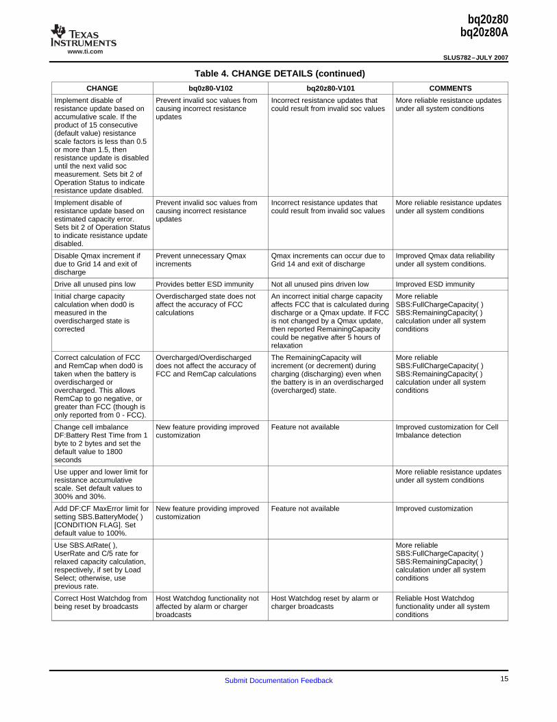
Table 4. CHANGE DETAILS
CHANGE bq0z80-V102 bq20z80-V101 COMMENTS
Corrected to allow display to LED display operates correctly LED display would stay on until Correct operation of the LEDturn off when charging and during charging. charging terminated after the button display under all conditionsbutton pushed. was pushed. Only occurs when LED
display not configured to be alwayson during charging.
13Submit Documentation Feedback
www.ti.com
bq20z80bq20z80A
SLUS782–JULY 2007
Table 4. CHANGE DETAILS (continued)
CHANGE bq0z80-V102 bq20z80-V101 COMMENTS
Allow negative LED Configuring negative LED alarm Feature not available Allow better customizationthresholds to permit LED threshold disables LED alarmalarms to be disabled functionality.
Allow zero values for ALARM Configuring zero value for the Feature not available Allow better customizationand CHARGING LED blink LED blink rates disables them.rates to disable them
Restore initialization of dodcharge initialized to the dodcharge value set to zero Improved gauging accuracy withdodcharge in relaxed state correct value correct initialization of dodchargeso that the correct dodcharge value.value is used in capacityestimation
Only clear offset calibration Prevents offset calibration Offset calibration occurs multiple More appropriate period betweenflag when SMBus lines go occurring just because a safety times if safety condition occurs offset calibrations when SMBushigh. condition occurs and then clears when SMBus lines are low. lines are low.
when the SMBus lines are low.
Change so that setting AFE Configurable option to allow Feature not available. Allow better customizationFail Limit to zero disables disabling PF_AFE_C triggerPF_AFE_C
Enable LED display to turn LED display turns off after charge LED display stays on when charging Correct operation of the LEDoff after charge termination termination. terminates after SMBus lines are display under all conditionsand if SMBus lines are detected low.detected low and LEDsenabled during charging.
Set charge FET state Charge FET state set correctly, The CHG FET would not get set to Quicker transition of FET to theimmediately when entering immediately after entering sleep the correct state for sleep until the correct state in sleepsleep first voltage measurement.
Change DF:Operation Cfg B Data flash default bases DF:Operation Cfg B [CCT = 1], Data flash default changed to[CCT = 0], so that SBS.CycleCount( ) calculation on making the default reflect common customer usageSBS.CycleCount( ) threshold mAh and not % of FCC SBS.CycleCount( ) calculation to beis in mAH, not in % of FCC based on % of FCC
When DF:Operation Cfg B Use DF:CC Threshold as the Small or negative SBS.Full Charge Improved system reliability[CCT = 1], so that minimum to prevent rapid Capacity( ) values (should not occurSBS.CycleCount( ) threshold incrementing of the under normal operation) fromis % of FCC, then DF:CC SBS.Cyclecount( ), damaging the causing the SBS.CycleCount( )Threshold is used as a data flash incrementing rapidly, potentiallyminimum for the damaging the data flashSBS.CycleCount( ) threshold
When exiting the relaxed Corrected initial charge capacity If the relaxed state was exited to More reliablestate to sleep, the initial calculation to be accurate when sleep after a valid DOD SBS:FullChargeCapacity( )charge capacity is correctly exiting relaxed state to sleep measurement (30-minute default calculation under all systemcalculated value), then the initial charge conditions
capacity would not be recalculatedand would result in an incorrect FCCvalue if the sleep state was exitedbefore another valid DODmeasurement (30-minute defaultvalue)
Correct update of Remcap in Charge or discharge current If the relaxed state was exited after More reliablerelaxed state to use passed accumulated in a relaxed state the accumulation of significant SBS:FullChargeCapacity( )charge used to update Remcap charge or discharge current (over at SBS:RemainingCapacity( )
most 100 seconds with default calculation under all systemvalues), the RemCap and FCC conditionswould be in error by this charge.This is only significant if the relaxedstate can exist with significantcurrent as determined by applicationsettings.
14 Submit Documentation Feedback
www.ti.com
bq20z80bq20z80A
SLUS782–JULY 2007
Table 4. CHANGE DETAILS (continued)
CHANGE bq0z80-V102 bq20z80-V101 COMMENTS
Implement disable of Prevent invalid soc values from Incorrect resistance updates that More reliable resistance updatesresistance update based on causing incorrect resistance could result from invalid soc values under all system conditionsaccumulative scale. If the updatesproduct of 15 consecutive(default value) resistancescale factors is less than 0.5or more than 1.5, thenresistance update is disableduntil the next valid socmeasurement. Sets bit 2 ofOperation Status to indicateresistance update disabled.
Implement disable of Prevent invalid soc values from Incorrect resistance updates that More reliable resistance updatesresistance update based on causing incorrect resistance could result from invalid soc values under all system conditionsestimated capacity error. updatesSets bit 2 of Operation Statusto indicate resistance updatedisabled.
Disable Qmax increment if Prevent unnecessary Qmax Qmax increments can occur due to Improved Qmax data reliabilitydue to Grid 14 and exit of increments Grid 14 and exit of discharge under all system conditions.discharge
Drive all unused pins low Provides better ESD immunity Not all unused pins driven low Improved ESD immunity
Initial charge capacity Overdischarged state does not An incorrect initial charge capacity More reliablecalculation when dod0 is affect the accuracy of FCC affects FCC that is calculated during SBS:FullChargeCapacity( )measured in the calculations discharge or a Qmax update. If FCC SBS:RemainingCapacity( )overdischarged state is is not changed by a Qmax update, calculation under all systemcorrected then reported RemainingCapacity conditions
could be negative after 5 hours ofrelaxation
Correct calculation of FCC Overcharged/Overdischarged The RemainingCapacity will More reliableand RemCap when dod0 is does not affect the accuracy of increment (or decrement) during SBS:FullChargeCapacity( )taken when the battery is FCC and RemCap calculations charging (discharging) even when SBS:RemainingCapacity( )overdischarged or the battery is in an overdischarged calculation under all systemovercharged. This allows (overcharged) state. conditionsRemCap to go negative, orgreater than FCC (though isonly reported from 0 - FCC).
Change cell imbalance New feature providing improved Feature not available Improved customization for CellDF:Battery Rest Time from 1 customization Imbalance detectionbyte to 2 bytes and set thedefault value to 1800seconds
Use upper and lower limit for More reliable resistance updatesresistance accumulative under all system conditionsscale. Set default values to300% and 30%.
Add DF:CF MaxError limit for New feature providing improved Feature not available Improved customizationsetting SBS.BatteryMode( ) customization[CONDITION FLAG]. Setdefault value to 100%.
Use SBS.AtRate( ), More reliableUserRate and C/5 rate for SBS:FullChargeCapacity( )relaxed capacity calculation, SBS:RemainingCapacity( )respectively, if set by Load calculation under all systemSelect; otherwise, use conditionsprevious rate.
Correct Host Watchdog from Host Watchdog functionality not Host Watchdog reset by alarm or Reliable Host Watchdogbeing reset by broadcasts affected by alarm or charger charger broadcasts functionality under all system
broadcasts conditions
15Submit Documentation Feedback
www.ti.com
bq20z80 to bq20z80-V101 Changes
bq20z80bq20z80A
SLUS782–JULY 2007
Table 4. CHANGE DETAILS (continued)
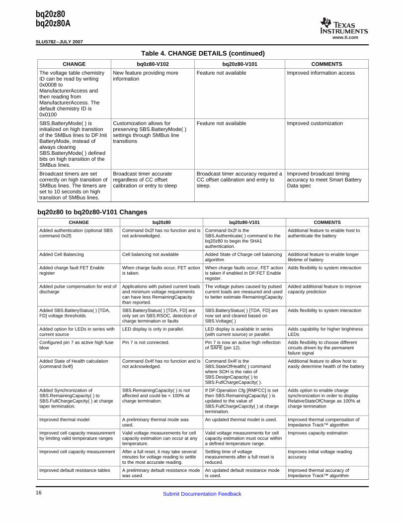
CHANGE bq0z80-V102 bq20z80-V101 COMMENTS
The voltage table chemistry New feature providing more Feature not available Improved information accessID can be read by writing information0x0008 toManufacturerAccess andthen reading fromManufacturerAccess. Thedefault chemistry ID is0x0100
SBS.BatteryMode( ) is Customization allows for Feature not available Improved customizationinitialized on high transition preserving SBS.BatteryMode( )of the SMBus lines to DF:Init settings through SMBus lineBatteryMode, instead of transitionsalways clearingSBS.BatteryMode( ) definedbits on high transition of theSMBus lines.
Broadcast timers are set Broadcast timer accurate Broadcast timer accuracy required a Improved broadcast timingcorrectly on high transition of regardless of CC offset CC offset calibration and entry to accuracy to meet Smart BatterySMBus lines. The timers are calibration or entry to sleep sleep. Data specset to 10 seconds on hightransition of SMBus lines.
CHANGE bq20z80 bq20z80-V101 COMMENTS
Added authentication (optional SBS Command 0x2f has no function and is Command 0x2f is the Additional feature to enable host tocommand 0x2f) not acknowledged. SBS.Authenticate( ) command to the authenticate the battery
bq20z80 to begin the SHA1authentication.
Added Cell Balancing Cell balancing not available Added State of Charge cell balancing Additional feature to enable longeralgorithm lifetime of battery
Added charge fault FET Enable When charge faults occur, FET action When charge faults occur, FET action Adds flexibility to system interactionregister is taken. is taken if enabled in DF:FET Enable
register.
Added pulse compensation for end of Applications with pulsed current loads The voltage pulses caused by pulsed Added additional feature to improvedischarge and minimum voltage requirements current loads are measured and used capacity prediction
can have less RemainingCapacity to better estimate RemainingCapacity.than reported.
Added SBS.BatteryStatus( ) [TDA, SBS.BatteryStatus( ) [TDA, FD] are SBS.BatteryStatus( ) [TDA, FD] are Adds flexibility to system interactionFD] voltage thresholds only set on SBS.RSOC, detection of now set and cleared based on
charge termination or faults SBS.Voltage( )
Added option for LEDs in series with LED display is only in parallel. LED display is available in series Adds capability for higher brightnesscurrent source (with current source) or parallel. LEDs
Configured pin 7 as active high fuse Pin 7 is not connected. Pin 7 is now an active high reflection Adds flexibility to choose differentblow of SAFE (pin 12). circuits driven by the permanent
failure signal
Added State of Health calculation Command 0x4f has no function and is Command 0x4f is the Additional feature to allow host to(command 0x4f) not acknowledged. SBS.StateOfHealth( ) command easily determine health of the battery
where SOH is the ratio ofSBS.DesignCapacity( ) toSBS.FullChargeCapacity( ).
Added Synchronization of SBS.RemainingCapacity( ) is not If DF:Operation Cfg [RMFCC] is set Adds option to enable chargeSBS.RemainingCapacity( ) to affected and could be < 100% at then SBS.RemainingCapacity( ) is synchronization in order to displaySBS.FullChargeCapcity( ) at charge charge termination. updated to the value of RelativeStateOfCharge as 100% attaper termination. SBS.FullChargeCapcity( ) at charge charge termination
termination.
Improved thermal model A preliminary thermal mode was An updated thermal model is used. Improved thermal compensation ofused. Impedance Track™ algorithm
Improved cell capacity measurement Valid voltage measurements for cell Valid voltage measurements for cell Improves capacity estimationby limiting valid temperature ranges capacity estimation can occur at any capacity estimation must occur within
temperature. a defined temperature range.
Improved cell capacity measurement After a full reset, it may take several Settling time of voltage Improves initial voltage readingminutes for voltage reading to settle measurements after a full reset is accuracyto the most accurate reading. reduced.
Improved default resistance tables A preliminary default resistance mode An updated default resistance mode Improved thermal accuracy ofwas used. is used. Impedance Track™ algorithm
16 Submit Documentation Feedback
www.ti.com
bq20z80bq20z80A
SLUS782–JULY 2007
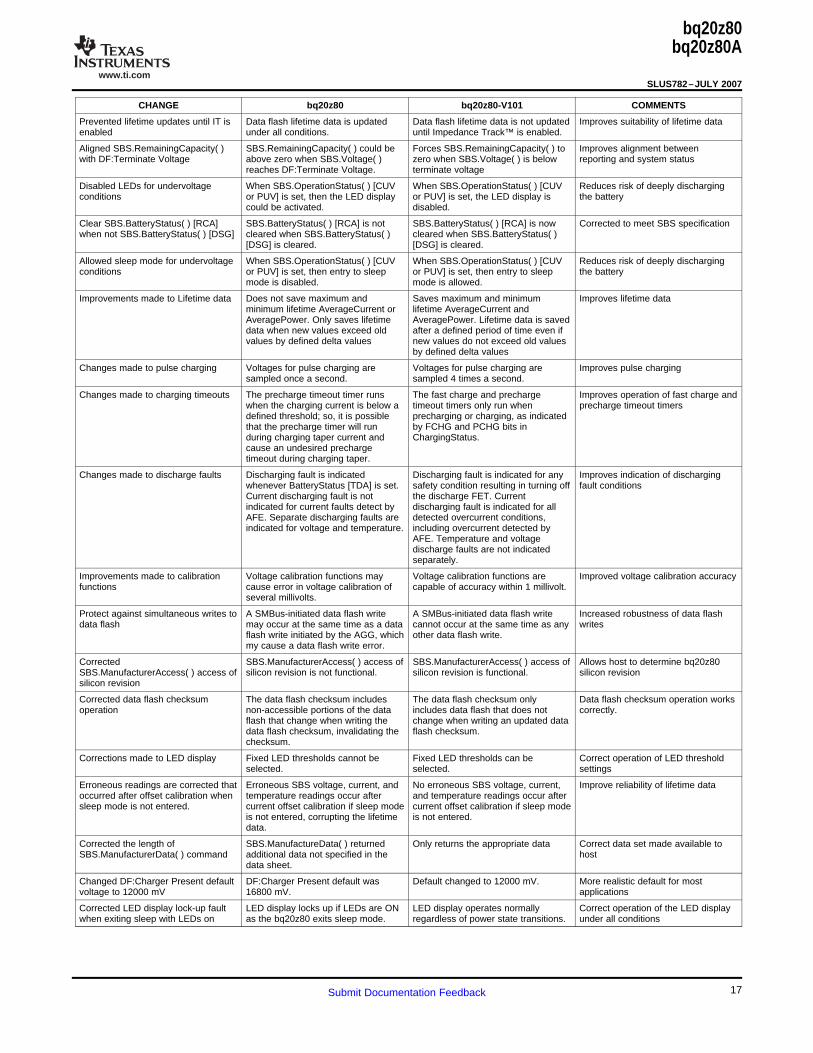
CHANGE bq20z80 bq20z80-V101 COMMENTS
Prevented lifetime updates until IT is Data flash lifetime data is updated Data flash lifetime data is not updated Improves suitability of lifetime dataenabled under all conditions. until Impedance Track™ is enabled.
Aligned SBS.RemainingCapacity( ) SBS.RemainingCapacity( ) could be Forces SBS.RemainingCapacity( ) to Improves alignment betweenwith DF:Terminate Voltage above zero when SBS.Voltage( ) zero when SBS.Voltage( ) is below reporting and system status
reaches DF:Terminate Voltage. terminate voltage
Disabled LEDs for undervoltage When SBS.OperationStatus( ) [CUV When SBS.OperationStatus( ) [CUV Reduces risk of deeply dischargingconditions or PUV] is set, then the LED display or PUV] is set, the LED display is the battery
could be activated. disabled.
Clear SBS.BatteryStatus( ) [RCA] SBS.BatteryStatus( ) [RCA] is not SBS.BatteryStatus( ) [RCA] is now Corrected to meet SBS specificationwhen not SBS.BatteryStatus( ) [DSG] cleared when SBS.BatteryStatus( ) cleared when SBS.BatteryStatus( )
[DSG] is cleared. [DSG] is cleared.
Allowed sleep mode for undervoltage When SBS.OperationStatus( ) [CUV When SBS.OperationStatus( ) [CUV Reduces risk of deeply dischargingconditions or PUV] is set, then entry to sleep or PUV] is set, then entry to sleep the battery
mode is disabled. mode is allowed.
Improvements made to Lifetime data Does not save maximum and Saves maximum and minimum Improves lifetime dataminimum lifetime AverageCurrent or lifetime AverageCurrent andAveragePower. Only saves lifetime AveragePower. Lifetime data is saveddata when new values exceed old after a defined period of time even ifvalues by defined delta values new values do not exceed old values
by defined delta values
Changes made to pulse charging Voltages for pulse charging are Voltages for pulse charging are Improves pulse chargingsampled once a second. sampled 4 times a second.
Changes made to charging timeouts The precharge timeout timer runs The fast charge and precharge Improves operation of fast charge andwhen the charging current is below a timeout timers only run when precharge timeout timersdefined threshold; so, it is possible precharging or charging, as indicatedthat the precharge timer will run by FCHG and PCHG bits induring charging taper current and ChargingStatus.cause an undesired prechargetimeout during charging taper.
Changes made to discharge faults Discharging fault is indicated Discharging fault is indicated for any Improves indication of dischargingwhenever BatteryStatus [TDA] is set. safety condition resulting in turning off fault conditionsCurrent discharging fault is not the discharge FET. Currentindicated for current faults detect by discharging fault is indicated for allAFE. Separate discharging faults are detected overcurrent conditions,indicated for voltage and temperature. including overcurrent detected by
AFE. Temperature and voltagedischarge faults are not indicatedseparately.
Improvements made to calibration Voltage calibration functions may Voltage calibration functions are Improved voltage calibration accuracyfunctions cause error in voltage calibration of capable of accuracy within 1 millivolt.
several millivolts.
Protect against simultaneous writes to A SMBus-initiated data flash write A SMBus-initiated data flash write Increased robustness of data flashdata flash may occur at the same time as a data cannot occur at the same time as any writes
flash write initiated by the AGG, which other data flash write.my cause a data flash write error.
Corrected SBS.ManufacturerAccess( ) access of SBS.ManufacturerAccess( ) access of Allows host to determine bq20z80SBS.ManufacturerAccess( ) access of silicon revision is not functional. silicon revision is functional. silicon revisionsilicon revision
Corrected data flash checksum The data flash checksum includes The data flash checksum only Data flash checksum operation worksoperation non-accessible portions of the data includes data flash that does not correctly.
flash that change when writing the change when writing an updated datadata flash checksum, invalidating the flash checksum.checksum.
Corrections made to LED display Fixed LED thresholds cannot be Fixed LED thresholds can be Correct operation of LED thresholdselected. selected. settings
Erroneous readings are corrected that Erroneous SBS voltage, current, and No erroneous SBS voltage, current, Improve reliability of lifetime dataoccurred after offset calibration when temperature readings occur after and temperature readings occur aftersleep mode is not entered. current offset calibration if sleep mode current offset calibration if sleep mode
is not entered, corrupting the lifetime is not entered.data.
Corrected the length of SBS.ManufactureData( ) returned Only returns the appropriate data Correct data set made available toSBS.ManufacturerData( ) command additional data not specified in the host
data sheet.
Changed DF:Charger Present default DF:Charger Present default was Default changed to 12000 mV. More realistic default for mostvoltage to 12000 mV 16800 mV. applications
Corrected LED display lock-up fault LED display locks up if LEDs are ON LED display operates normally Correct operation of the LED displaywhen exiting sleep with LEDs on as the bq20z80 exits sleep mode. regardless of power state transitions. under all conditions
17Submit Documentation Feedback
www.ti.com
bq20z80bq20z80A
SLUS782–JULY 2007
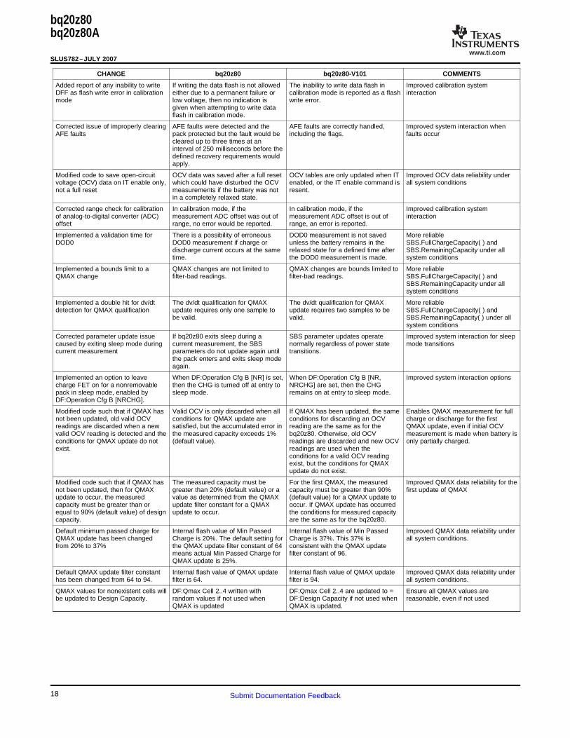
CHANGE bq20z80 bq20z80-V101 COMMENTS
Added report of any inability to write If writing the data flash is not allowed The inability to write data flash in Improved calibration systemDFF as flash write error in calibration either due to a permanent failure or calibration mode is reported as a flash interactionmode low voltage, then no indication is write error.
given when attempting to write dataflash in calibration mode.
Corrected issue of improperly clearing AFE faults were detected and the AFE faults are correctly handled, Improved system interaction whenAFE faults pack protected but the fault would be including the flags. faults occur
cleared up to three times at aninterval of 250 milliseconds before thedefined recovery requirements wouldapply.
Modified code to save open-circuit OCV data was saved after a full reset OCV tables are only updated when IT Improved OCV data reliability undervoltage (OCV) data on IT enable only, which could have disturbed the OCV enabled, or the IT enable command is all system conditionsnot a full reset measurements if the battery was not resent.
in a completely relaxed state.
Corrected range check for calibration In calibration mode, if the In calibration mode, if the Improved calibration systemof analog-to-digital converter (ADC) measurement ADC offset was out of measurement ADC offset is out of interactionoffset range, no error would be reported. range, an error is reported.
Implemented a validation time for There is a possibility of erroneous DOD0 measurement is not saved More reliableDOD0 DOD0 measurement if charge or unless the battery remains in the SBS.FullChargeCapacity( ) and
discharge current occurs at the same relaxed state for a defined time after SBS.RemainingCapacity under alltime. the DOD0 measurement is made. system conditions
Implemented a bounds limit to a QMAX changes are not limited to QMAX changes are bounds limited to More reliableQMAX change filter-bad readings. filter-bad readings. SBS.FullChargeCapacity( ) and
SBS.RemainingCapacity under allsystem conditions
Implemented a double hit for dv/dt The dv/dt qualification for QMAX The dv/dt qualification for QMAX More reliabledetection for QMAX qualification update requires only one sample to update requires two samples to be SBS.FullChargeCapacity( ) and
be valid. valid. SBS.RemainingCapacity( ) under allsystem conditions
Corrected parameter update issue If bq20z80 exits sleep during a SBS parameter updates operate Improved system interaction for sleepcaused by exiting sleep mode during current measurement, the SBS normally regardless of power state mode transitionscurrent measurement parameters do not update again until transitions.
the pack enters and exits sleep modeagain.
Implemented an option to leave When DF:Operation Cfg B [NR] is set, When DF:Operation Cfg B [NR, Improved system interaction optionscharge FET on for a nonremovable then the CHG is turned off at entry to NRCHG] are set, then the CHGpack in sleep mode, enabled by sleep mode. remains on at entry to sleep mode.DF:Operation Cfg B [NRCHG].
Modified code such that if QMAX has Valid OCV is only discarded when all If QMAX has been updated, the same Enables QMAX measurement for fullnot been updated, old valid OCV conditions for QMAX update are conditions for discarding an OCV charge or discharge for the firstreadings are discarded when a new satisfied, but the accumulated error in reading are the same as for the QMAX update, even if initial OCVvalid OCV reading is detected and the the measured capacity exceeds 1% bq20z80. Otherwise, old OCV measurement is made when battery isconditions for QMAX update do not (default value). readings are discarded and new OCV only partially charged.exist. readings are used when the
conditions for a valid OCV readingexist, but the conditions for QMAXupdate do not exist.
Modified code such that if QMAX has The measured capacity must be For the first QMAX, the measured Improved QMAX data reliability for thenot been updated, then for QMAX greater than 20% (default value) or a capacity must be greater than 90% first update of QMAXupdate to occur, the measured value as determined from the QMAX (default value) for a QMAX update tocapacity must be greater than or update filter constant for a QMAX occur. If QMAX update has occurredequal to 90% (default value) of design update to occur. the conditions for measured capacitycapacity. are the same as for the bq20z80.
Default minimum passed charge for Internal flash value of Min Passed Internal flash value of Min Passed Improved QMAX data reliability underQMAX update has been changed Charge is 20%. The default setting for Charge is 37%. This 37% is all system conditions.from 20% to 37% the QMAX update filter constant of 64 consistent with the QMAX update
means actual Min Passed Charge for filter constant of 96.QMAX update is 25%.
Default QMAX update filter constant Internal flash value of QMAX update Internal flash value of QMAX update Improved QMAX data reliability underhas been changed from 64 to 94. filter is 64. filter is 94. all system conditions.
QMAX values for nonexistent cells will DF:Qmax Cell 2..4 written with DF:Qmax Cell 2..4 are updated to = Ensure all QMAX values arebe updated to Design Capacity. random values if not used when DF:Design Capacity if not used when reasonable, even if not used
QMAX is updated QMAX is updated.
18 Submit Documentation Feedback
PACKAGE OPTION ADDENDUM
www.ti.com 20-Aug-2011
Addendum-Page 1
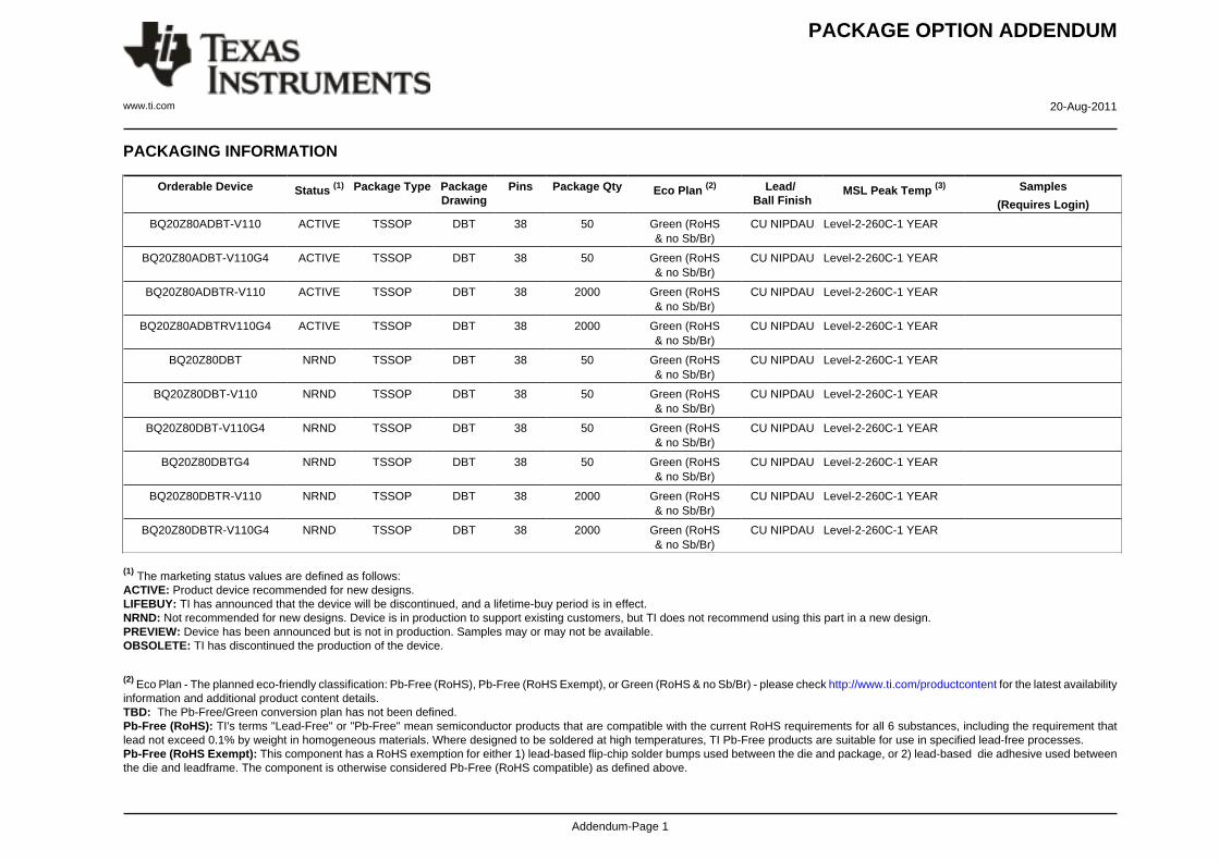
PACKAGING INFORMATION
Orderable Device Status (1) Package Type PackageDrawing
Pins Package Qty Eco Plan (2) Lead/Ball Finish
MSL Peak Temp (3) Samples
(Requires Login)
BQ20Z80ADBT-V110 ACTIVE TSSOP DBT 38 50 Green (RoHS& no Sb/Br)
CU NIPDAU Level-2-260C-1 YEAR
BQ20Z80ADBT-V110G4 ACTIVE TSSOP DBT 38 50 Green (RoHS& no Sb/Br)
CU NIPDAU Level-2-260C-1 YEAR
BQ20Z80ADBTR-V110 ACTIVE TSSOP DBT 38 2000 Green (RoHS& no Sb/Br)
CU NIPDAU Level-2-260C-1 YEAR
BQ20Z80ADBTRV110G4 ACTIVE TSSOP DBT 38 2000 Green (RoHS& no Sb/Br)
CU NIPDAU Level-2-260C-1 YEAR
BQ20Z80DBT NRND TSSOP DBT 38 50 Green (RoHS& no Sb/Br)
CU NIPDAU Level-2-260C-1 YEAR
BQ20Z80DBT-V110 NRND TSSOP DBT 38 50 Green (RoHS& no Sb/Br)
CU NIPDAU Level-2-260C-1 YEAR
BQ20Z80DBT-V110G4 NRND TSSOP DBT 38 50 Green (RoHS& no Sb/Br)
CU NIPDAU Level-2-260C-1 YEAR
BQ20Z80DBTG4 NRND TSSOP DBT 38 50 Green (RoHS& no Sb/Br)
CU NIPDAU Level-2-260C-1 YEAR
BQ20Z80DBTR-V110 NRND TSSOP DBT 38 2000 Green (RoHS& no Sb/Br)
CU NIPDAU Level-2-260C-1 YEAR
BQ20Z80DBTR-V110G4 NRND TSSOP DBT 38 2000 Green (RoHS& no Sb/Br)
CU NIPDAU Level-2-260C-1 YEAR
(1) The marketing status values are defined as follows:ACTIVE: Product device recommended for new designs.LIFEBUY: TI has announced that the device will be discontinued, and a lifetime-buy period is in effect.NRND: Not recommended for new designs. Device is in production to support existing customers, but TI does not recommend using this part in a new design.PREVIEW: Device has been announced but is not in production. Samples may or may not be available.OBSOLETE: TI has discontinued the production of the device.
(2) Eco Plan - The planned eco-friendly classification: Pb-Free (RoHS), Pb-Free (RoHS Exempt), or Green (RoHS & no Sb/Br) - please check http://www.ti.com/productcontent for the latest availabilityinformation and additional product content details.TBD: The Pb-Free/Green conversion plan has not been defined.Pb-Free (RoHS): TI's terms "Lead-Free" or "Pb-Free" mean semiconductor products that are compatible with the current RoHS requirements for all 6 substances, including the requirement thatlead not exceed 0.1% by weight in homogeneous materials. Where designed to be soldered at high temperatures, TI Pb-Free products are suitable for use in specified lead-free processes.Pb-Free (RoHS Exempt): This component has a RoHS exemption for either 1) lead-based flip-chip solder bumps used between the die and package, or 2) lead-based die adhesive used betweenthe die and leadframe. The component is otherwise considered Pb-Free (RoHS compatible) as defined above.
PACKAGE OPTION ADDENDUM
www.ti.com 20-Aug-2011
Addendum-Page 2
Green (RoHS & no Sb/Br): TI defines "Green" to mean Pb-Free (RoHS compatible), and free of Bromine (Br) and Antimony (Sb) based flame retardants (Br or Sb do not exceed 0.1% by weightin homogeneous material)
(3) MSL, Peak Temp. -- The Moisture Sensitivity Level rating according to the JEDEC industry standard classifications, and peak solder temperature.
Important Information and Disclaimer:The information provided on this page represents TI's knowledge and belief as of the date that it is provided. TI bases its knowledge and belief on informationprovided by third parties, and makes no representation or warranty as to the accuracy of such information. Efforts are underway to better integrate information from third parties. TI has taken andcontinues to take reasonable steps to provide representative and accurate information but may not have conducted destructive testing or chemical analysis on incoming materials and chemicals.TI and TI suppliers consider certain information to be proprietary, and thus CAS numbers and other limited information may not be available for release.
In no event shall TI's liability arising out of such information exceed the total purchase price of the TI part(s) at issue in this document sold by TI to Customer on an annual basis.
TAPE AND REEL INFORMATION
*All dimensions are nominal
Device PackageType
PackageDrawing
Pins SPQ ReelDiameter
(mm)
ReelWidth
W1 (mm)
A0(mm)
B0(mm)
K0(mm)
P1(mm)
W(mm)
Pin1Quadrant
BQ20Z80ADBTR-V110 TSSOP DBT 38 2000 330.0 16.4 6.9 10.2 1.8 12.0 16.0 Q1
PACKAGE MATERIALS INFORMATION
www.ti.com 14-Jul-2012
Pack Materials-Page 1
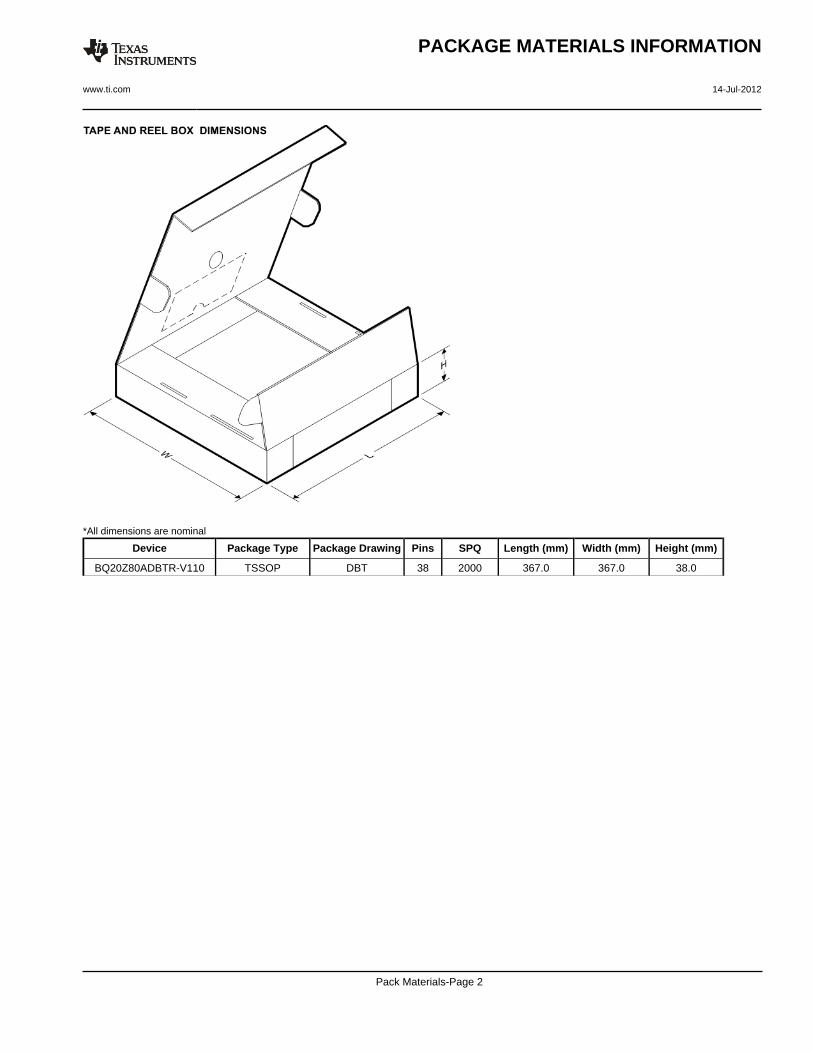
*All dimensions are nominal
Device Package Type Package Drawing Pins SPQ Length (mm) Width (mm) Height (mm)
BQ20Z80ADBTR-V110 TSSOP DBT 38 2000 367.0 367.0 38.0
PACKAGE MATERIALS INFORMATION
www.ti.com 14-Jul-2012
Pack Materials-Page 2
IMPORTANT NOTICE
Texas Instruments Incorporated and its subsidiaries (TI) reserve the right to make corrections, enhancements, improvements and otherchanges to its semiconductor products and services per JESD46C and to discontinue any product or service per JESD48B. Buyers shouldobtain the latest relevant information before placing orders and should verify that such information is current and complete. Allsemiconductor products (also referred to herein as “components”) are sold subject to TI’s terms and conditions of sale supplied at the timeof order acknowledgment.
TI warrants performance of its components to the specifications applicable at the time of sale, in accordance with the warranty in TI’s termsand conditions of sale of semiconductor products. Testing and other quality control techniques are used to the extent TI deems necessaryto support this warranty. Except where mandated by applicable law, testing of all parameters of each component is not necessarilyperformed.
TI assumes no liability for applications assistance or the design of Buyers’ products. Buyers are responsible for their products andapplications using TI components. To minimize the risks associated with Buyers’ products and applications, Buyers should provideadequate design and operating safeguards.
TI does not warrant or represent that any license, either express or implied, is granted under any patent right, copyright, mask work right, orother intellectual property right relating to any combination, machine, or process in which TI components or services are used. Informationpublished by TI regarding third-party products or services does not constitute a license to use such products or services or a warranty orendorsement thereof. Use of such information may require a license from a third party under the patents or other intellectual property of thethird party, or a license from TI under the patents or other intellectual property of TI.
Reproduction of significant portions of TI information in TI data books or data sheets is permissible only if reproduction is without alterationand is accompanied by all associated warranties, conditions, limitations, and notices. TI is not responsible or liable for such altereddocumentation. Information of third parties may be subject to additional restrictions.
Resale of TI components or services with statements different from or beyond the parameters stated by TI for that component or servicevoids all express and any implied warranties for the associated TI component or service and is an unfair and deceptive business practice.TI is not responsible or liable for any such statements.
Buyer acknowledges and agrees that it is solely responsible for compliance with all legal, regulatory and safety-related requirementsconcerning its products, and any use of TI components in its applications, notwithstanding any applications-related information or supportthat may be provided by TI. Buyer represents and agrees that it has all the necessary expertise to create and implement safeguards whichanticipate dangerous consequences of failures, monitor failures and their consequences, lessen the likelihood of failures that might causeharm and take appropriate remedial actions. Buyer will fully indemnify TI and its representatives against any damages arising out of the useof any TI components in safety-critical applications.
In some cases, TI components may be promoted specifically to facilitate safety-related applications. With such components, TI’s goal is tohelp enable customers to design and create their own end-product solutions that meet applicable functional safety standards andrequirements. Nonetheless, such components are subject to these terms.
No TI components are authorized for use in FDA Class III (or similar life-critical medical equipment) unless authorized officers of the partieshave executed a special agreement specifically governing such use.
Only those TI components which TI has specifically designated as military grade or “enhanced plastic” are designed and intended for use inmilitary/aerospace applications or environments. Buyer acknowledges and agrees that any military or aerospace use of TI componentswhich have not been so designated is solely at the Buyer's risk, and that Buyer is solely responsible for compliance with all legal andregulatory requirements in connection with such use.
TI has specifically designated certain components which meet ISO/TS16949 requirements, mainly for automotive use. Components whichhave not been so designated are neither designed nor intended for automotive use; and TI will not be responsible for any failure of suchcomponents to meet such requirements.
Products Applications
Audio www.ti.com/audio Automotive and Transportation www.ti.com/automotive
Amplifiers amplifier.ti.com Communications and Telecom www.ti.com/communications
Data Converters dataconverter.ti.com Computers and Peripherals www.ti.com/computers
DLP® Products www.dlp.com Consumer Electronics www.ti.com/consumer-apps
DSP dsp.ti.com Energy and Lighting www.ti.com/energy
Clocks and Timers www.ti.com/clocks Industrial www.ti.com/industrial
Interface interface.ti.com Medical www.ti.com/medical
Logic logic.ti.com Security www.ti.com/security
Power Mgmt power.ti.com Space, Avionics and Defense www.ti.com/space-avionics-defense
Microcontrollers microcontroller.ti.com Video and Imaging www.ti.com/video
RFID www.ti-rfid.com
OMAP Mobile Processors www.ti.com/omap TI E2E Community e2e.ti.com
Wireless Connectivity www.ti.com/wirelessconnectivity
Mailing Address: Texas Instruments, Post Office Box 655303, Dallas, Texas 75265Copyright © 2012, Texas Instruments Incorporated