Embed Size (px)
Citation preview
ADS8326
REF5025
REF
VOUT
GND
+IN
-IN
VIN+5 V
OPA365
InputSignal
0 V to 4 V
5 V 5 V
VDD
GND
C
1 Fm
BYPASS
R
50 W
1
C
1.2 nF1
C
22 Fm
2
Copyright © 2016, Texas Instruments IncorporatedCopyright © 2016, Texas Instruments Incorporated
Product
Folder
Sample &Buy
Technical
Documents
Tools &
Software
Support &Community
An IMPORTANT NOTICE at the end of this data sheet addresses availability, warranty, changes, use in safety-critical applications,intellectual property matters and other important disclaimers. PRODUCTION DATA.
REF5025-HTSBOS502F –SEPTEMBER 2009–REVISED DECEMBER 2016
REF5025-HT Low-Noise, Very-Low-Drift, Precision Voltage Reference
1
(1) Custom temperature ranges available
1 Features1• Low Temperature Drift: 40 ppm/°C• Low Noise: 3 μVPP/V• High Output Current: ±7 mA• Low Temperature Drift:
5 ppm/°C (Maximum)• Available in Military (–55°C to +210°C)
Temperature Range (1)
• Extended Product Life Cycle• Extended Product-Change Notification• Product Traceability
2 Applications• 16-Bit Data Acquisition Systems• ATE Equipment• Industrial Process Control• Medical Instrumentation• Optical Control Systems• Precision Instrumentation• Controlled Baseline• One Assembly and Test Site• One Fabrication Site
3 DescriptionThe REF5025-HT is a low-noise, very low-drift, veryhigh precision voltage references. This reference iscapable of both sinking and sourcing, and is veryrobust with regard to line and load changes.
Excellent temperature drift and high accuracy areachieved using proprietary design techniques. Thesefeatures, combined with very low noise, make theREF5025-HT suitable for use in high-precision dataacquisition systems.
The device is offered in HKJ and HKQ packages, aswell as Known-Good-Die (KGD) form, and is specifiedfrom –55°C to +210°C.
Device Information(a)PART NUMBER PACKAGE BODY SIZE (NOM)
REF5025-HTCFP (HKJ)(8) 6.9 mm × 5.65 mmCFP (HKQ) (8) 6.9 mm × 5.65 mmXCEPT (KGD) (0) 2.04 mm × 1.676 mm
(a) For all available packages, see the orderable addendum atthe end of the data sheet.
Simplified Schematic
2
REF5025-HTSBOS502F –SEPTEMBER 2009–REVISED DECEMBER 2016 www.ti.com
Product Folder Links: REF5025-HT
Submit Documentation Feedback Copyright © 2009–2016, Texas Instruments Incorporated
Table of Contents1 Features .................................................................. 12 Applications ........................................................... 13 Description ............................................................. 14 Revision History..................................................... 25 Pin Configuration and Functions ......................... 36 Specifications......................................................... 5
6.1 Absolute Maximum Ratings ..................................... 56.2 ESD Ratings.............................................................. 56.3 Recommended Operating Conditions....................... 56.4 Thermal Information .................................................. 56.5 Electrical Characteristics........................................... 66.6 Typical Characteristics .............................................. 8
7 Detailed Description ............................................ 127.1 Overview ................................................................. 127.2 Functional Block Diagram ....................................... 127.3 Feature Description................................................. 127.4 Device Functional Modes........................................ 14
8 Application and Implementation ........................ 158.1 Application Information............................................ 158.2 Typical Applications ............................................... 158.3 System Example ..................................................... 19
9 Power Supply Recommendations ...................... 2110 Layout................................................................... 22
10.1 Layout Guidelines ................................................. 2210.2 Layout Example .................................................... 2210.3 Power Dissipation ................................................. 22
11 Device and Documentation Support ................. 2311.1 Documentation Support ....................................... 2311.2 Receiving Notification of Documentation Updates 2311.3 Community Resources.......................................... 2311.4 Trademarks ........................................................... 2311.5 Electrostatic Discharge Caution............................ 2311.6 Glossary ................................................................ 23
12 Mechanical, Packaging, and OrderableInformation ........................................................... 23
4 Revision HistoryNOTE: Page numbers for previous revisions may differ from page numbers in the current version.
Changes from Revision E (November 2013) to Revision F Page
• Added ESD Ratings table, Feature Description section, Device Functional Modes, Application and Implementationsection, Power Supply Recommendations section, Layout section, Device and Documentation Support section, andMechanical, Packaging, and Orderable Information section ................................................................................................. 1
• Deleted Ordering Information table, see POA at the end of the data sheet........................................................................... 1
Changes from Revision D (April 2012) to Revision E Page
• Added KGD2 package option ................................................................................................................................................ 1
1
2
3
4
8
7
6
5
DNC
VIN
TEMP
GNDTRIM/NR
VOUT
NC
DNC1
2
3
4
8
7
6
5
DNC
VIN
TEMP
GND TRIM/NR
VOUT
NC
DNC
3
REF5025-HTwww.ti.com SBOS502F –SEPTEMBER 2009–REVISED DECEMBER 2016
Product Folder Links: REF5025-HT
Submit Documentation FeedbackCopyright © 2009–2016, Texas Instruments Incorporated
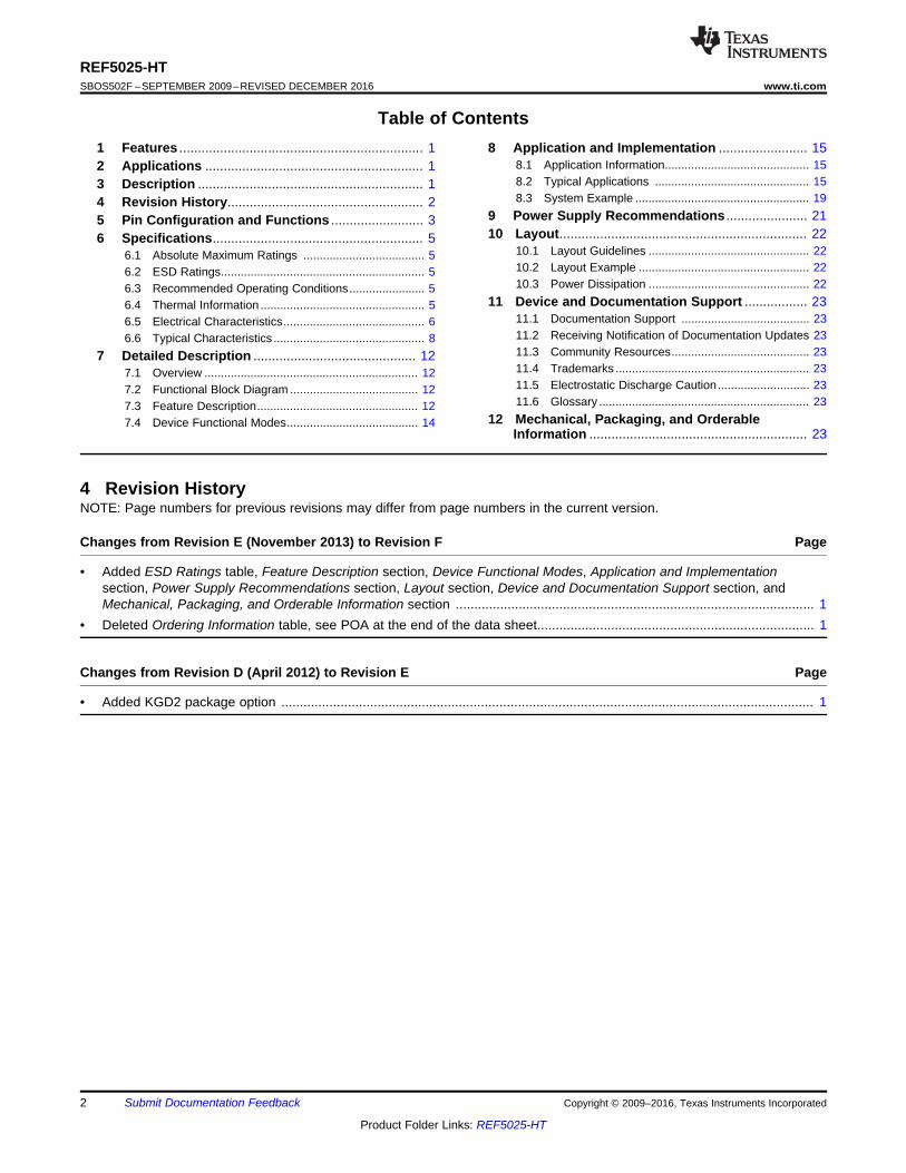
5 Pin Configuration and Functions
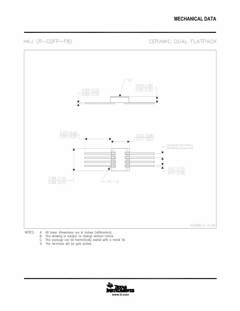
HKJ Package8-Pin CFPTop View
DNC = Do not connectNC = No internal connection
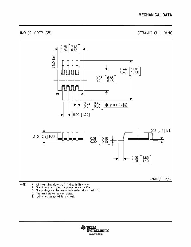
HKQ Package8-Pin CFPTop View
HKQ is a dead bug performed version ofHKJ
Pin FunctionsPIN
I/O DESCRIPTIONNAME NO.DNC 1, 8 — Do not connectGND 4 Power System groundNC 7 — No internal connectionTEMP 3 O Temperature monitoring pin provides a temperature-dependent voltage output
TRIM/NR 5 I Output adjustment and noise reduction input. Connecting 1 μF to this pin creates a low-pass filter at the bandgap and reduce output noise
VIN 2 Power Power supply voltage. Range from VOUT + 0.2 V up to 18 V. TI recommends a bypasscapacitor with a value from 1 μF up to 10 μF
VOUT 6 O Very accurate, factory-trimmed voltage output. TI recommends a bypass capacitor with avalue from 1 μF up to 50 μF with ESR between 1 and 1.5 Ω
0.0
0.0
1 2 3 4 5 6 7
9 8101112
½ ½2040 mm
½½
|
38 mm
|38 mm
1676 µ
m
4
REF5025-HTSBOS502F –SEPTEMBER 2009–REVISED DECEMBER 2016 www.ti.com
Product Folder Links: REF5025-HT
Submit Documentation Feedback Copyright © 2009–2016, Texas Instruments Incorporated
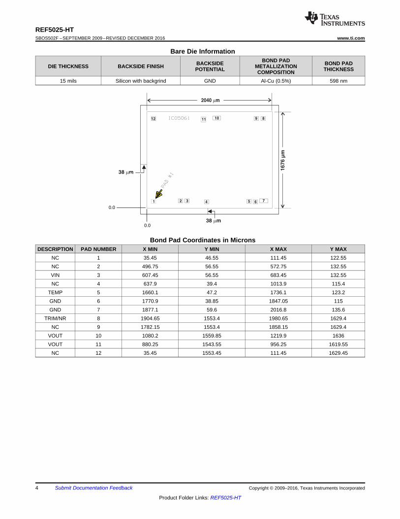
Bare Die Information
DIE THICKNESS BACKSIDE FINISH BACKSIDEPOTENTIAL
BOND PADMETALLIZATIONCOMPOSITION
BOND PADTHICKNESS
15 mils Silicon with backgrind GND Al-Cu (0.5%) 598 nm
Bond Pad Coordinates in MicronsDESCRIPTION PAD NUMBER X MIN Y MIN X MAX Y MAX
NC 1 35.45 46.55 111.45 122.55NC 2 496.75 56.55 572.75 132.55VIN 3 607.45 56.55 683.45 132.55NC 4 637.9 39.4 1013.9 115.4
TEMP 5 1660.1 47.2 1736.1 123.2GND 6 1770.9 38.85 1847.05 115GND 7 1877.1 59.6 2016.8 135.6
TRIM/NR 8 1904.65 1553.4 1980.65 1629.4NC 9 1782.15 1553.4 1858.15 1629.4
VOUT 10 1080.2 1559.85 1219.9 1636VOUT 11 880.25 1543.55 956.25 1619.55
NC 12 35.45 1553.45 111.45 1629.45
5
REF5025-HTwww.ti.com SBOS502F –SEPTEMBER 2009–REVISED DECEMBER 2016
Product Folder Links: REF5025-HT
Submit Documentation FeedbackCopyright © 2009–2016, Texas Instruments Incorporated
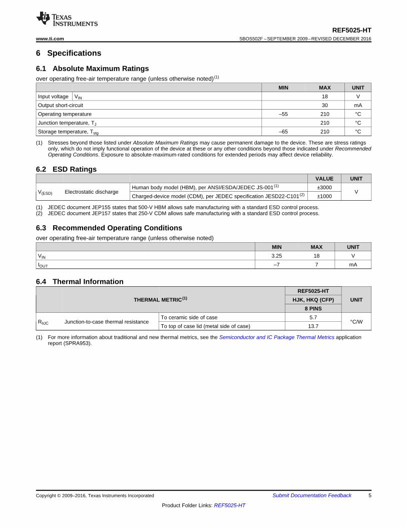
(1) Stresses beyond those listed under Absolute Maximum Ratings may cause permanent damage to the device. These are stress ratingsonly, which do not imply functional operation of the device at these or any other conditions beyond those indicated under RecommendedOperating Conditions. Exposure to absolute-maximum-rated conditions for extended periods may affect device reliability.
6 Specifications
6.1 Absolute Maximum Ratingsover operating free-air temperature range (unless otherwise noted) (1)
MIN MAX UNITInput voltage VIN 18 VOutput short-circuit 30 mAOperating temperature –55 210 °CJunction temperature, TJ 210 °CStorage temperature, Tstg –65 210 °C
(1) JEDEC document JEP155 states that 500-V HBM allows safe manufacturing with a standard ESD control process.(2) JEDEC document JEP157 states that 250-V CDM allows safe manufacturing with a standard ESD control process.
6.2 ESD RatingsVALUE UNIT
V(ESD) Electrostatic dischargeHuman body model (HBM), per ANSI/ESDA/JEDEC JS-001 (1) ±3000
VCharged-device model (CDM), per JEDEC specification JESD22-C101 (2) ±1000
6.3 Recommended Operating Conditionsover operating free-air temperature range (unless otherwise noted)
MIN MAX UNITVIN 3.25 18 VIOUT –7 7 mA
(1) For more information about traditional and new thermal metrics, see the Semiconductor and IC Package Thermal Metrics applicationreport (SPRA953).
6.4 Thermal Information
THERMAL METRIC (1)REF5025-HT
UNITHJK, HKQ (CFP)8 PINS
RθJC Junction-to-case thermal resistanceTo ceramic side of case 5.7
°C/WTo top of case lid (metal side of case) 13.7
6
REF5025-HTSBOS502F –SEPTEMBER 2009–REVISED DECEMBER 2016 www.ti.com
Product Folder Links: REF5025-HT
Submit Documentation Feedback Copyright © 2009–2016, Texas Instruments Incorporated
(1) See Figure 5.(2) See Figure 4.(3) See Figure 10.
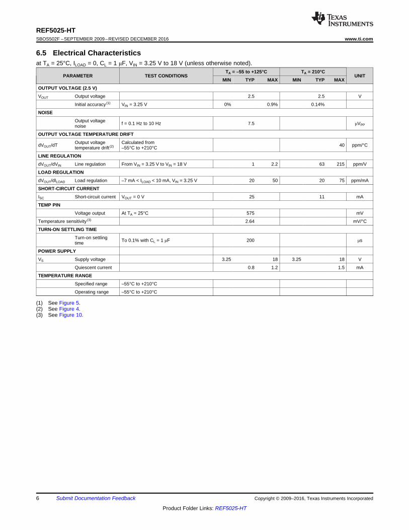
6.5 Electrical Characteristicsat TA = 25°C, ILOAD = 0, CL = 1 μF, VIN = 3.25 V to 18 V (unless otherwise noted).
PARAMETER TEST CONDITIONSTA = –55 to +125°C TA = 210°C
UNITMIN TYP MAX MIN TYP MAX
OUTPUT VOLTAGE (2.5 V)
VOUT Output voltage 2.5 2.5 V
Initial accuracy (1) VIN = 3.25 V 0% 0.9% 0.14%
NOISE
Output voltagenoise f = 0.1 Hz to 10 Hz 7.5 μVPP
OUTPUT VOLTAGE TEMPERATURE DRIFT
dVOUT/dT Output voltagetemperature drift (2)
Calculated from–55°C to +210°C 40 ppm/°C
LINE REGULATION
dVOUT/dVIN Line regulation From VIN = 3.25 V to VIN = 18 V 1 2.2 63 215 ppm/V
LOAD REGULATION
dVOUT/dILOAD Load regulation –7 mA < ILOAD < 10 mA, VIN = 3.25 V 20 50 20 75 ppm/mA
SHORT-CIRCUIT CURRENT
ISC Short-circuit current VOUT = 0 V 25 11 mA
TEMP PIN
Voltage output At TA = 25°C 575 mV
Temperature sensitivity (3) 2.64 mV/°C
TURN-ON SETTLING TIME
Turn-on settlingtime To 0.1% with CL = 1 μF 200 μs
POWER SUPPLY
VS Supply voltage 3.25 18 3.25 18 V
Quiescent current 0.8 1.2 1.5 mA
TEMPERATURE RANGE
Specified range –55°C to +210°C
Operating range –55°C to +210°C
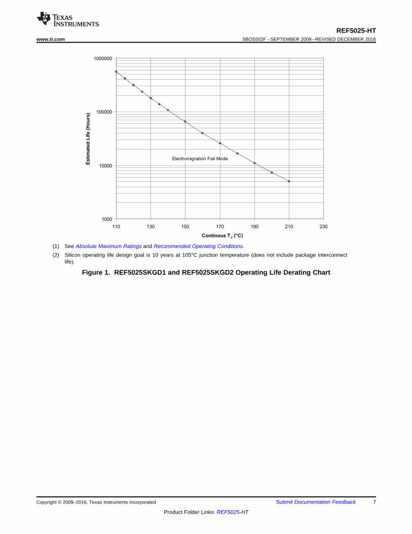
1000
10000
100000
1000000
110 130 150 170 190 210 230
Continous TJ (°C)
Esti
mate
dL
ife
(Ho
urs
)
Electromigration Fail Mode
7
REF5025-HTwww.ti.com SBOS502F –SEPTEMBER 2009–REVISED DECEMBER 2016
Product Folder Links: REF5025-HT
Submit Documentation FeedbackCopyright © 2009–2016, Texas Instruments Incorporated
(1) See Absolute Maximum Ratings and Recommended Operating Conditions.(2) Silicon operating life design goal is 10 years at 105°C junction temperature (does not include package interconnect
life).
Figure 1. REF5025SKGD1 and REF5025SKGD2 Operating Life Derating Chart
10
Frequency (Hz)
160
140
120
100
80
60
40
20
0
PS
RR
(dB
)
100k100 1k 10k
-0.2
-0.1
0
0.1
0.2
0.3
0.4
0.5
-55 25 125 180 210
Temperature (°C)
Ou
tpu
tV
olt
ag
eA
cc
ura
cy
(%)
2 610
14
18
22
26
30
34
38
42
46
50
54
Drift (ppm/°C)
Po
pu
lati
on
(%)
-0
.6
-0
.5
-0
.4
-0
.3
-0
.2
-0
.1 0
0.1
0.2
0.3
0.4
0.5
0.6
Mo
re
Output Initial Accuracy(%)
Po
pu
lati
on
(%)
0
0.2
5
0.5
0
0.7
5
1.0
0
1.2
5
1.5
0
1.7
5
2.0
0
2.2
5
2.5
0
2.7
5
3.0
0
3.2
5
3.5
0
3.7
5
4.0
0
4.2
5
4.5
0
4.7
5
5.0
0
Drift (ppm/ C)°
Po
pu
latio
n (
%)
0
0.5
0
1.0
0
1.5
0
2.0
0
2.5
0
3.0
0
3.5
0
4.0
0
4.5
0
5.0
0
5.5
0
6.0
0
6.5
0
7.0
0
7.5
0
8.0
0
Drift (ppm/ C)°
Po
pu
latio
n (
%)
8
REF5025-HTSBOS502F –SEPTEMBER 2009–REVISED DECEMBER 2016 www.ti.com
Product Folder Links: REF5025-HT
Submit Documentation Feedback Copyright © 2009–2016, Texas Instruments Incorporated
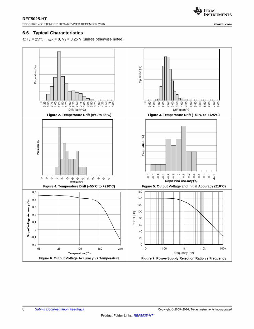
6.6 Typical Characteristicsat TA = 25°C, ILOAD = 0, VS = 3.25 V (unless otherwise noted).
Figure 2. Temperature Drift (0°C to 85°C) Figure 3. Temperature Drift (–40°C to +125°C)
Figure 4. Temperature Drift (–55°C to +210°C) Figure 5. Output Voltage and Initial Accuracy (210°C)
Figure 6. Output Voltage Accuracy vs Temperature Figure 7. Power-Supply Rejection Ratio vs Frequency
210°C
25°C
–55°C
600
700
800
900
1000
1100
1200
1300
1400
2 3 4 5 6 7 8 9 10 11 12 13 14 15 16 17 18
VIN (V)
IQ(µ
A)
-10
0
10
20
30
40
50
60
70
-75 -50 -25 0 25 50 75 100 125 150 175 200 225
Temperature (°C)
Lin
eR
eg
ula
tio
n(p
pm
/V)
600
700
800
900
1000
1100
1200
-75 -50 -25 0 25 50 75 100 125 150 175 200 225
Temperature (°C)
IQ(µ
A)
0.3
0.4
0.5
0.6
0.7
0.8
0.9
1
1.1
-75 -50 -25 0 25 50 75 100 125 150 175 200 225
Temperature (°C)
Tem
pP
inO
utp
utV
oltag
e(V
)
55°C
25°C
210°C
2.494
2.496
2.498
2.5
2.502
2.504
2.506
2.508
2.51
2.512
2.514
-10 -5 0 5 10
Load Current (mA)
Outp
utV
oltage
(V)
-15 -10 -5
Load Current (mA)
0.8
0.7
0.6
0.5
0.4
0.3
0.2
0.1
0
Dro
po
ut V
olta
ge
(V
)
150 5 10
+125 C°
+25 C°
- °40 C
9
REF5025-HTwww.ti.com SBOS502F –SEPTEMBER 2009–REVISED DECEMBER 2016
Product Folder Links: REF5025-HT
Submit Documentation FeedbackCopyright © 2009–2016, Texas Instruments Incorporated
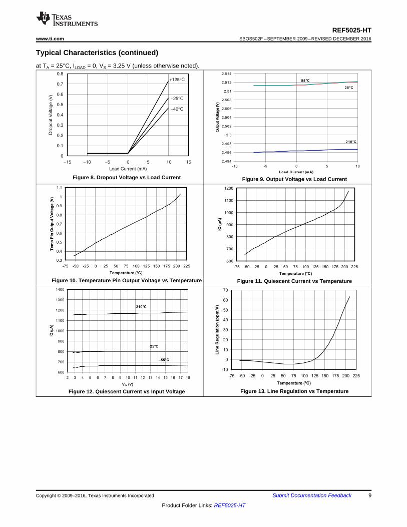
Typical Characteristics (continued)at TA = 25°C, ILOAD = 0, VS = 3.25 V (unless otherwise noted).
Figure 8. Dropout Voltage vs Load Current Figure 9. Output Voltage vs Load Current
Figure 10. Temperature Pin Output Voltage vs Temperature Figure 11. Quiescent Current vs Temperature
Figure 12. Quiescent Current vs Input Voltage Figure 13. Line Regulation vs Temperature
20 s/divm
-1mA -1mA
+1mA
ILOAD
VOUT
5mV/div
1mA/div
20 s/divm
-10mA
+10mA+10mA
ILOAD
VOUT
2mV/div
10mA/div
40 s/divm
2V/div
1V/divVOUT
VIN
400 s/divm
5V/div
1V/div
VOUT
VIN
1s/div
1V
/div
m
Sinking
Sourcing
0
5
10
15
20
25
30
-75 -50 -25 0 25 50 75 100 125 150 175 200
Temperature (°C)
Sh
ort
-Cir
cu
itC
urr
en
t(m
A)
10
REF5025-HTSBOS502F –SEPTEMBER 2009–REVISED DECEMBER 2016 www.ti.com
Product Folder Links: REF5025-HT
Submit Documentation Feedback Copyright © 2009–2016, Texas Instruments Incorporated
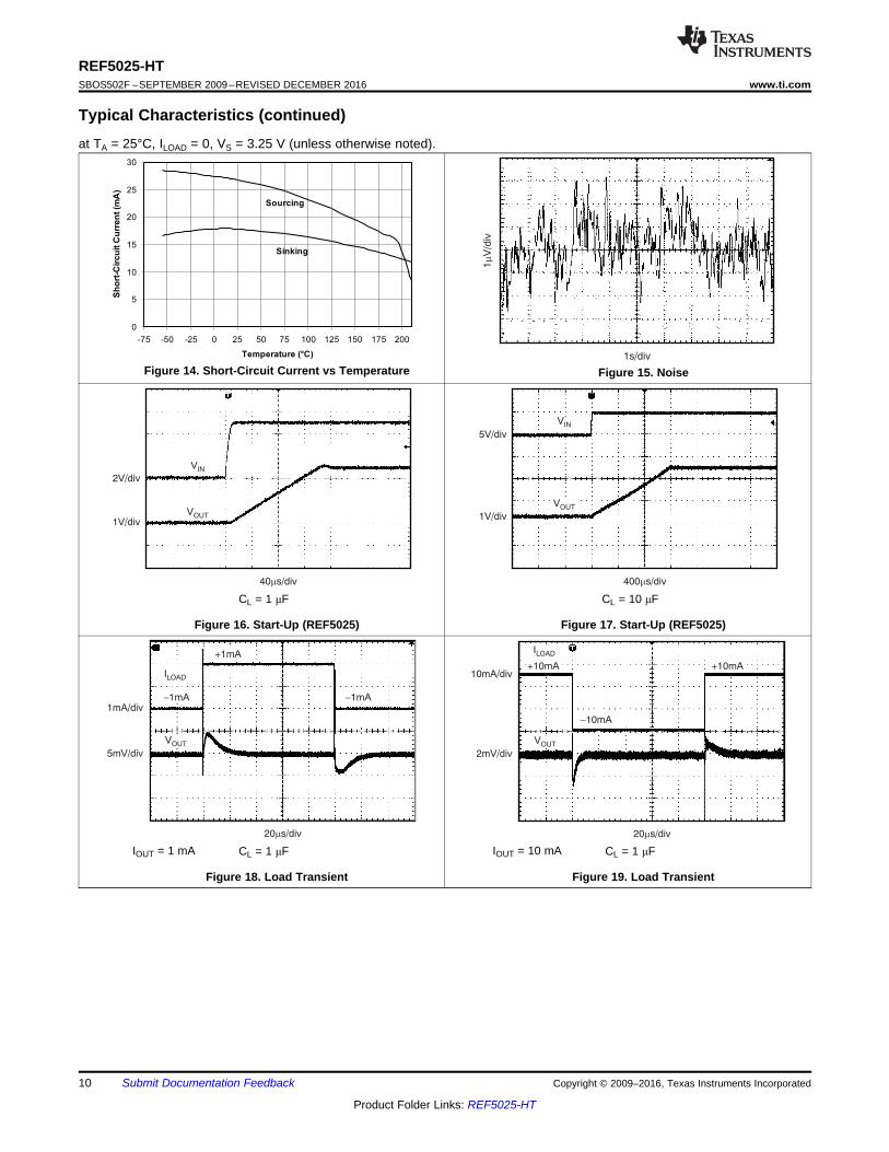
Typical Characteristics (continued)at TA = 25°C, ILOAD = 0, VS = 3.25 V (unless otherwise noted).
Figure 14. Short-Circuit Current vs Temperature Figure 15. Noise
CL = 1 μF
Figure 16. Start-Up (REF5025)
CL = 10 μF
Figure 17. Start-Up (REF5025)
IOUT = 1 mA CL = 1 μF
Figure 18. Load Transient
IOUT = 10 mA CL = 1 μF
Figure 19. Load Transient
20ms/div
VOUT
VIN
5mV/div
500mV/div
100 s/divm
VOUT
VIN
5mV/div
500mV/div
100 s/divm
-1mA -1mA
+1mA
ILOAD
VOUT
5mV/div
1mA/div
100 s/divm
-10mA -10mA
+10mAILOAD
VOUT
2mV/div
10mA/div
11
REF5025-HTwww.ti.com SBOS502F –SEPTEMBER 2009–REVISED DECEMBER 2016
Product Folder Links: REF5025-HT
Submit Documentation FeedbackCopyright © 2009–2016, Texas Instruments Incorporated
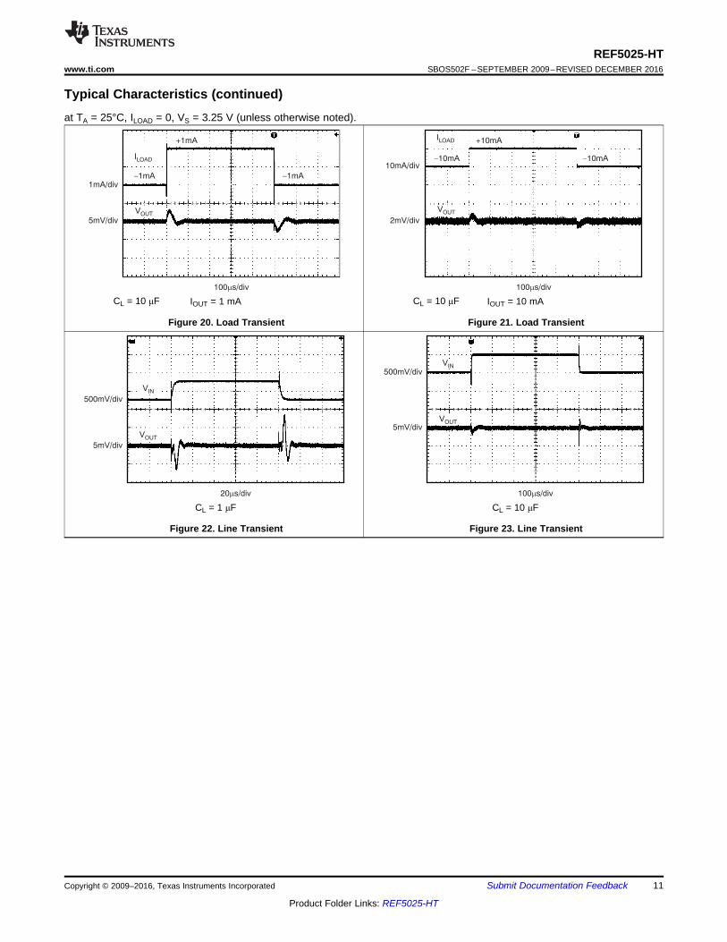
Typical Characteristics (continued)at TA = 25°C, ILOAD = 0, VS = 3.25 V (unless otherwise noted).
CL = 10 μF IOUT = 1 mA
Figure 20. Load Transient
CL = 10 μF IOUT = 10 mA
Figure 21. Load Transient
CL = 1 μF
Figure 22. Line Transient
CL = 10 μF
Figure 23. Line Transient
DNC
TEMP VOUT
VIN
GND
DNC
NC
TRIM/NR
REF5025
+VSUPPLY
10kW
1kW
470W
Copyright © 2016, Texas Instruments Incorporated
R560kW
REF5025
TEMP VOUT
GND
TRIM/NR
VIN
aT
aT(10mA
at +25°C)
R2 R1
R3
R4
10kW
1kW1.2V
Copyright © 2016, Texas Instruments Incorporated
12
REF5025-HTSBOS502F –SEPTEMBER 2009–REVISED DECEMBER 2016 www.ti.com
Product Folder Links: REF5025-HT
Submit Documentation Feedback Copyright © 2009–2016, Texas Instruments Incorporated
7 Detailed Description
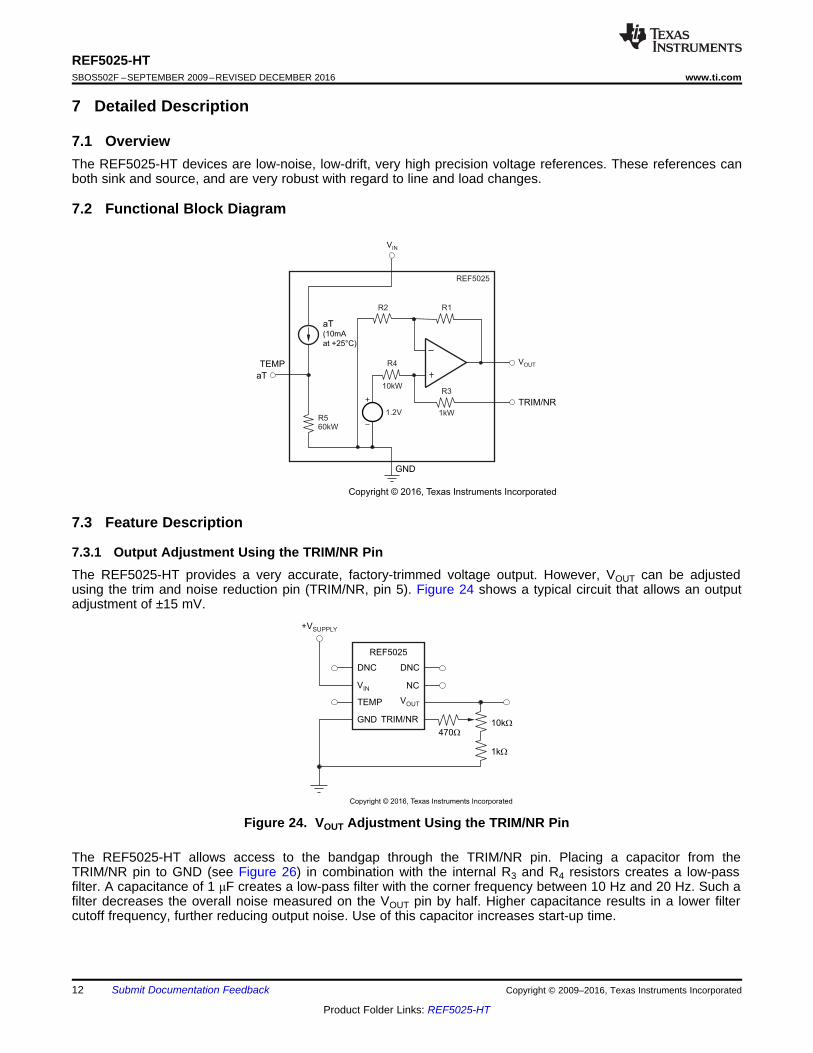
7.1 OverviewThe REF5025-HT devices are low-noise, low-drift, very high precision voltage references. These references canboth sink and source, and are very robust with regard to line and load changes.
7.2 Functional Block Diagram
7.3 Feature Description
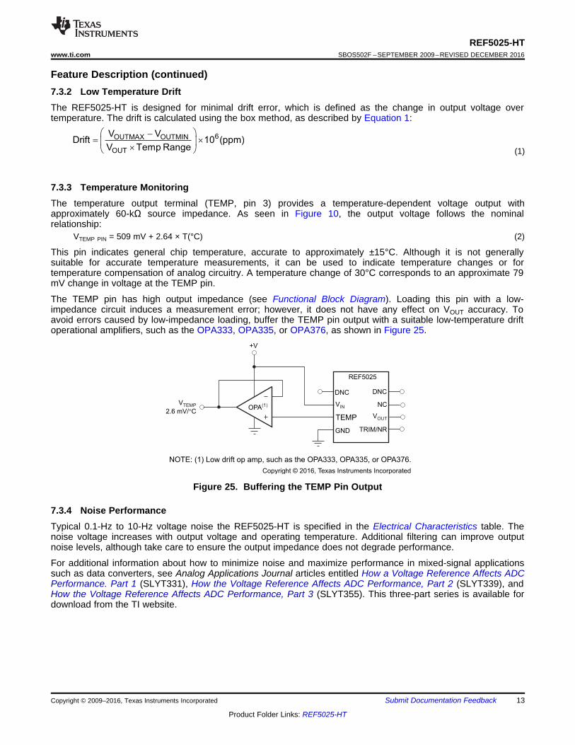
7.3.1 Output Adjustment Using the TRIM/NR PinThe REF5025-HT provides a very accurate, factory-trimmed voltage output. However, VOUT can be adjustedusing the trim and noise reduction pin (TRIM/NR, pin 5). Figure 24 shows a typical circuit that allows an outputadjustment of ±15 mV.
Figure 24. VOUT Adjustment Using the TRIM/NR Pin
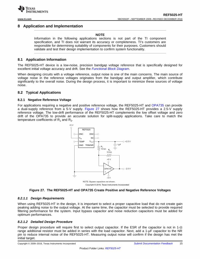
The REF5025-HT allows access to the bandgap through the TRIM/NR pin. Placing a capacitor from theTRIM/NR pin to GND (see Figure 26) in combination with the internal R3 and R4 resistors creates a low-passfilter. A capacitance of 1 μF creates a low-pass filter with the corner frequency between 10 Hz and 20 Hz. Such afilter decreases the overall noise measured on the VOUT pin by half. Higher capacitance results in a lower filtercutoff frequency, further reducing output noise. Use of this capacitor increases start-up time.
DNC
TEMP VOUT
VIN
GND
DNC
NC
TRIM/NR
REF5025
VTEMP
2.6 mV/ C°OPA(1)
NOTE: (1) Low drift op amp, such as the OPA333, OPA335, or OPA376.
+V
Copyright © 2016, Texas Instruments Incorporated
6OUTMAX OUTMIN
OUT
V VDrift 10 (ppm)
V Temp Range
æ ö-= ´ç ÷
´è ø
13
REF5025-HTwww.ti.com SBOS502F –SEPTEMBER 2009–REVISED DECEMBER 2016
Product Folder Links: REF5025-HT
Submit Documentation FeedbackCopyright © 2009–2016, Texas Instruments Incorporated
Feature Description (continued)7.3.2 Low Temperature DriftThe REF5025-HT is designed for minimal drift error, which is defined as the change in output voltage overtemperature. The drift is calculated using the box method, as described by Equation 1:
(1)
7.3.3 Temperature MonitoringThe temperature output terminal (TEMP, pin 3) provides a temperature-dependent voltage output withapproximately 60-kΩ source impedance. As seen in Figure 10, the output voltage follows the nominalrelationship:
VTEMP PIN = 509 mV + 2.64 × T(°C) (2)
This pin indicates general chip temperature, accurate to approximately ±15°C. Although it is not generallysuitable for accurate temperature measurements, it can be used to indicate temperature changes or fortemperature compensation of analog circuitry. A temperature change of 30°C corresponds to an approximate 79mV change in voltage at the TEMP pin.
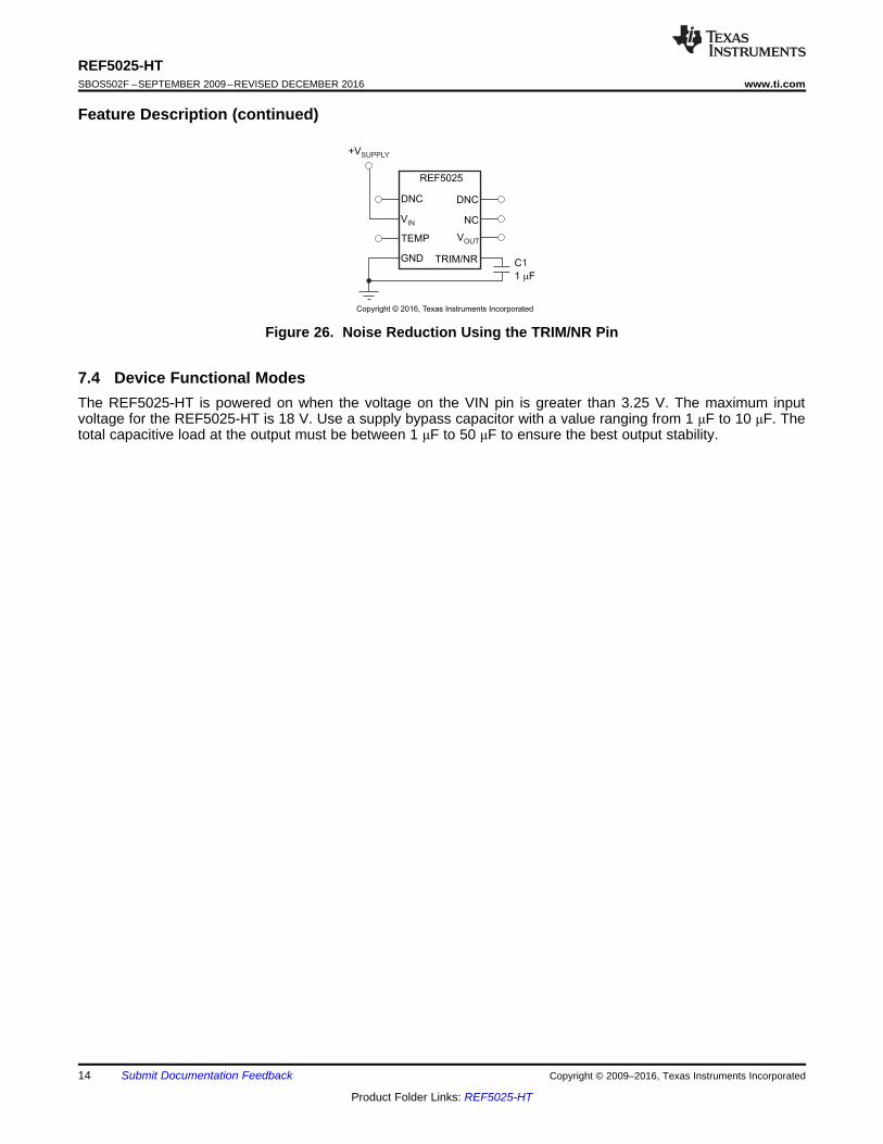
The TEMP pin has high output impedance (see Functional Block Diagram). Loading this pin with a low-impedance circuit induces a measurement error; however, it does not have any effect on VOUT accuracy. Toavoid errors caused by low-impedance loading, buffer the TEMP pin output with a suitable low-temperature driftoperational amplifiers, such as the OPA333, OPA335, or OPA376, as shown in Figure 25.
Figure 25. Buffering the TEMP Pin Output
7.3.4 Noise PerformanceTypical 0.1-Hz to 10-Hz voltage noise the REF5025-HT is specified in the Electrical Characteristics table. Thenoise voltage increases with output voltage and operating temperature. Additional filtering can improve outputnoise levels, although take care to ensure the output impedance does not degrade performance.
For additional information about how to minimize noise and maximize performance in mixed-signal applicationssuch as data converters, see Analog Applications Journal articles entitled How a Voltage Reference Affects ADCPerformance. Part 1 (SLYT331), How the Voltage Reference Affects ADC Performance, Part 2 (SLYT339), andHow the Voltage Reference Affects ADC Performance, Part 3 (SLYT355). This three-part series is available fordownload from the TI website.
DNC
TEMP VOUT
VIN
GND
DNC
NC
TRIM/NR
REF5025
C1
1 Fm
+VSUPPLY
Copyright © 2016, Texas Instruments Incorporated
14
REF5025-HTSBOS502F –SEPTEMBER 2009–REVISED DECEMBER 2016 www.ti.com
Product Folder Links: REF5025-HT
Submit Documentation Feedback Copyright © 2009–2016, Texas Instruments Incorporated
Feature Description (continued)
Figure 26. Noise Reduction Using the TRIM/NR Pin
7.4 Device Functional ModesThe REF5025-HT is powered on when the voltage on the VIN pin is greater than 3.25 V. The maximum inputvoltage for the REF5025-HT is 18 V. Use a supply bypass capacitor with a value ranging from 1 μF to 10 μF. Thetotal capacitive load at the output must be between 1 μF to 50 μF to ensure the best output stability.
-2.5 V
+2.5 V
+5 V
NOTE: Bypass capacitors not shown.
R1
10 kW R2
10 kW
-5 V
OPA735
+5 V
DNC
TEMP VOUT
VIN
GND
DNC
NC
TRIM/NR
REF5025
1 Fm
Copyright © 2016, Texas Instruments Incorporated
15
REF5025-HTwww.ti.com SBOS502F –SEPTEMBER 2009–REVISED DECEMBER 2016
Product Folder Links: REF5025-HT
Submit Documentation FeedbackCopyright © 2009–2016, Texas Instruments Incorporated
8 Application and Implementation
NOTEInformation in the following applications sections is not part of the TI componentspecification, and TI does not warrant its accuracy or completeness. TI’s customers areresponsible for determining suitability of components for their purposes. Customers shouldvalidate and test their design implementation to confirm system functionality.
8.1 Application InformationThe REF5025-HT device is a low-noise, precision bandgap voltage reference that is specifically designed forexcellent initial voltage accuracy and drift. See the Functional Block Diagram.
When designing circuits with a voltage reference, output noise is one of the main concerns. The main source ofvoltage noise in the reference voltages originates from the bandgap and output amplifier, which contributesignificantly to the overall noise. During the design process, it is important to minimize these sources of voltagenoise.
8.2 Typical Applications
8.2.1 Negative Reference VoltageFor applications requiring a negative and positive reference voltage, the REF5025-HT and OPA735 can providea dual-supply reference from a 5-V supply. Figure 27 shows how the REF5025-HT provides a 2.5-V supplyreference voltage. The low-drift performance of the REF5025-HT complements the low offset voltage and zerodrift of the OPA735 to provide an accurate solution for split-supply applications. Take care to match thetemperature coefficients of R1 and R2.
Figure 27. The REF5025-HT and OPA735 Create Positive and Negative Reference Voltages
8.2.1.1 Design RequirementsWhen using REF5025-HT in the design, it is important to select a proper capacitive load that do not create gainpeaking adding noise to the output voltage. At the same time, the capacitor must be selected to provide requiredfiltering performance for the system. Input bypass capacitor and noise reduction capacitors must be added foroptimum performances.
8.2.1.2 Detailed Design ProcedureProper design procedure will require first to select output capacitor. If the ESR of the capacitor is not in 1-Ωrange additional resistor must be added in series with the load capacitor. Next, add a 1-µF capacitor to the NRpin to reduce internal noise of the REF5025-HT. Measuring output noise will confirm if the design has met theinitial target.
NC
VIN
TEMP
GND
REF5025
1 8 NC
Variable
+2.5 V
C
1 µF - 50 µFOUT
+5 V
C
10 µFIN
2
3
4
NC
VOUT
TRIM
7
6
5
Copyright © 2016, Texas Instruments Incorporated
16
REF5025-HTSBOS502F –SEPTEMBER 2009–REVISED DECEMBER 2016 www.ti.com
Product Folder Links: REF5025-HT
Submit Documentation Feedback Copyright © 2009–2016, Texas Instruments Incorporated
Typical Applications (continued)8.2.1.3 Application Curves
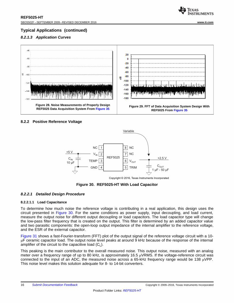
Figure 28. Noise Measurements of Properly DesignREF5025 Data Acquisition System From Figure 35
Figure 29. FFT of Data Acquisition System Design WithREF5025 From Figure 35
8.2.2 Positive Reference Voltage
Figure 30. REF5025-HT With Load Capacitor
8.2.2.1 Detailed Design Procedure
8.2.2.1.1 Load Capacitance
To determine how much noise the reference voltage is contributing in a real application, this design uses thecircuit presented in Figure 30. For the same conditions as power supply, input decoupling, and load current,measure the output noise for different output decoupling or load capacitors. The load capacitor type will changethe low-pass filter frequency that is created on the output. This filter is determined by an added capacitor valueand two parasitic components: the open-loop output impedance of the internal amplifier to the reference voltage,and the ESR of the external capacitor.
Figure 31 shows a fast-Fourier-transform (FFT) plot of the output signal of the reference voltage circuit with a 10-μF ceramic capacitor load. The output noise level peaks at around 9 kHz because of the response of the internalamplifier of the circuit to the capacitive load (CL).
This peaking is the main contributor to the overall measured noise. This output noise, measured with an analogmeter over a frequency range of up to 80 kHz, is approximately 16.5 μVRMS. If the voltage-reference circuit wasconnected to the input of an ADC, the measured noise across a 65-kHz frequency range would be 138 μVPP.This noise level makes this solution adequate for 8- to 14-bit converters.
VCC
ESR
CL
RO
PL
1ƒ
2 • (R ESR) • C=
p +
ZL
1ƒ
2 • ESR • C=
p
17
REF5025-HTwww.ti.com SBOS502F –SEPTEMBER 2009–REVISED DECEMBER 2016
Product Folder Links: REF5025-HT
Submit Documentation FeedbackCopyright © 2009–2016, Texas Instruments Incorporated
Typical Applications (continued)
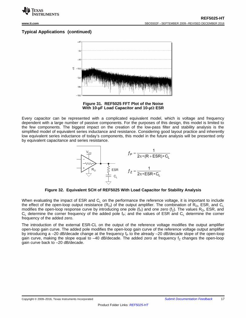
Figure 31. REF5025 FFT Plot of the NoiseWith 10-µF Load Capacitor and 10-µΩ ESR
Every capacitor can be represented with a complicated equivalent model, which is voltage and frequencydependent with a large number of passive components. For the purposes of this design, this model is limited tothe few components. The biggest impact on the creation of the low-pass filter and stability analysis is thesimplified model of equivalent series inductance and resistance. Considering good layout practice and inherentlylow equivalent series inductance of today’s components, this model in the future analysis will be presented onlyby equivalent capacitance and series resistance.
Figure 32. Equivalent SCH of REF5025 With Load Capacitor for Stability Analysis
When evaluating the impact of ESR and CL on the performance the reference voltage, it is important to includethe effect of the open-loop output resistance (RO) of the output amplifier. The combination of RO, ESR, and CLmodifies the open-loop response curve by introducing one pole (fP) and one zero (fZ). The values RO, ESR, andCL determine the corner frequency of the added pole fP; and the values of ESR and CL determine the cornerfrequency of the added zero.
The introduction of the external ESR-CL on the output of the reference voltage modifies the output amplifieropen-loop gain curve. The added pole modifies the open-loop gain curve of the reference voltage output amplifierby introducing a –20 dB/decade change at the frequency fP to the already –20 dB/decade slope of the open-loopgain curve, making the slope equal to –40 dB/decade. The added zero at frequency fZ changes the open-loopgain curve back to –20 dB/decade.
VOUT
TRIM
R2 R1
10k
1k
1.2V
18
REF5025-HTSBOS502F –SEPTEMBER 2009–REVISED DECEMBER 2016 www.ti.com
Product Folder Links: REF5025-HT
Submit Documentation Feedback Copyright © 2009–2016, Texas Instruments Incorporated
Typical Applications (continued)Table 1. Noise Measurement Results for Different Load Capacitors
NOISE 22 kHzLP-5P
30 kHzLP-3P
80 kHzLP-3P > 500 kHz UNIT
GND 0.8 1 1.8 4.9
µVRMS
1 µF 37.8 41.7 53.7 90172.2 µF (cer) 41.7 46.2 55.1 60.8
10 µF 33.4 33.4 35.2 38.510 µF (cer) 37.1 37.2 37.8 39.120 µF (cer) 33.1 33.1 33.2 34.5
47 µF 23.2 23.8 24.1 26.5
Table 1 shows the measured noise values for different frequency bandwidths as well as different values andtypes of external capacitors. These measurements show that low-ESR (approximately 100-mΩ) ceramiccapacitors tend to increase the noise, compared to normal-ESR (approximately 2-Ω) tantalum capacitors. Thistendency is caused by a stability issue with the output amplifier and gain peaking in the amplifier frequencyresponse.
8.2.2.1.2 Bandgap Noise Reduction
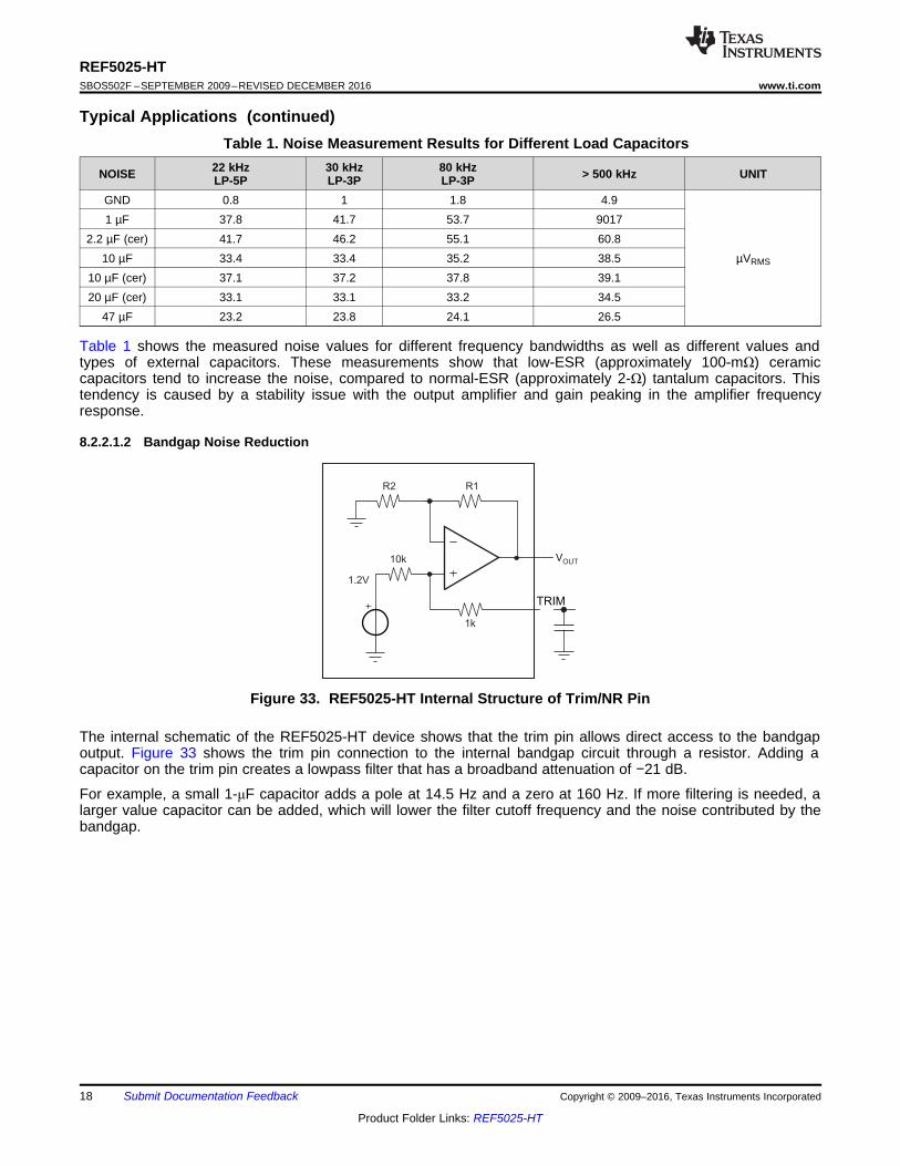
Figure 33. REF5025-HT Internal Structure of Trim/NR Pin
The internal schematic of the REF5025-HT device shows that the trim pin allows direct access to the bandgapoutput. Figure 33 shows the trim pin connection to the internal bandgap circuit through a resistor. Adding acapacitor on the trim pin creates a lowpass filter that has a broadband attenuation of −21 dB.
For example, a small 1-μF capacitor adds a pole at 14.5 Hz and a zero at 160 Hz. If more filtering is needed, alarger value capacitor can be added, which will lower the filter cutoff frequency and the noise contributed by thebandgap.
ADS8326
CS
CLK
SDO
1 nF
124 W
10 uF
ESR
47 uF
0-4 V
OPA365
REF5040
REFIN
Copyright © 2016, Texas Instruments Incorporated
ADS8326
REF5040
REF
VOUT
GND
+IN
-IN
VIN+5 V
OPA365
InputSignal
0 V to 4 V
+5 V +5 V
VDD
GND
CBYPASS
1 Fm
R1
50 W
C1
1.2 nF
C2
22 Fm
Copyright © 2016, Texas Instruments Incorporated
19
REF5025-HTwww.ti.com SBOS502F –SEPTEMBER 2009–REVISED DECEMBER 2016
Product Folder Links: REF5025-HT
Submit Documentation FeedbackCopyright © 2009–2016, Texas Instruments Incorporated
Table 2. Measured Noise (µVRMS) for Four Bandwidths
NOISE 22 kHz (LOW-PASS5-POLE)
30 kHz (LOW-PASS3-POLE)
80 kHz (LOW-PASS 3-POLE) > 500 kHz UNIT
GND 0.8 1 1.8 4.6
µVRMS
2.2 µF (ceramic) 42.5 47.2 61.2 68.32.2 µF + 1 µF 17.5 19.4 22.6 24.5
10 µF (ceramic) 34.4 35.6 37.7 44.510 µF + 1 µF 14.1 14.4 14.9 16.4
20 µF (ceramic) 34.8 34.9 35.1 35.220 µF + 1 µF 14.4 14.4 14.7 15.1
Adding a 1-μF capacitor in this example filters the noise contribution of the bandgap and lowers the total noise bya factor of 2.5 times.
8.3 System Example
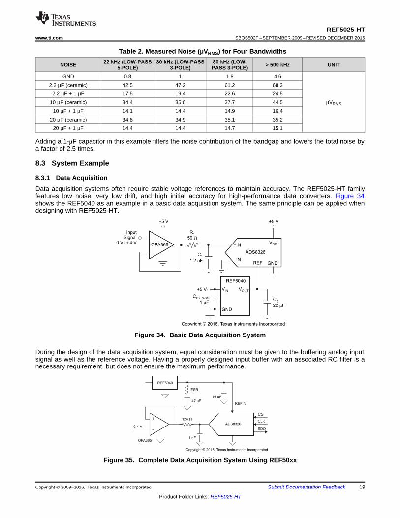
8.3.1 Data AcquisitionData acquisition systems often require stable voltage references to maintain accuracy. The REF5025-HT familyfeatures low noise, very low drift, and high initial accuracy for high-performance data converters. Figure 34shows the REF5040 as an example in a basic data acquisition system. The same principle can be applied whendesigning with REF5025-HT.
Figure 34. Basic Data Acquisition System
During the design of the data acquisition system, equal consideration must be given to the buffering analog inputsignal as well as the reference voltage. Having a properly designed input buffer with an associated RC filter is anecessary requirement, but does not ensure the maximum performance.
Figure 35. Complete Data Acquisition System Using REF50xx
20
REF5025-HTSBOS502F –SEPTEMBER 2009–REVISED DECEMBER 2016 www.ti.com
Product Folder Links: REF5025-HT
Submit Documentation Feedback Copyright © 2009–2016, Texas Instruments Incorporated
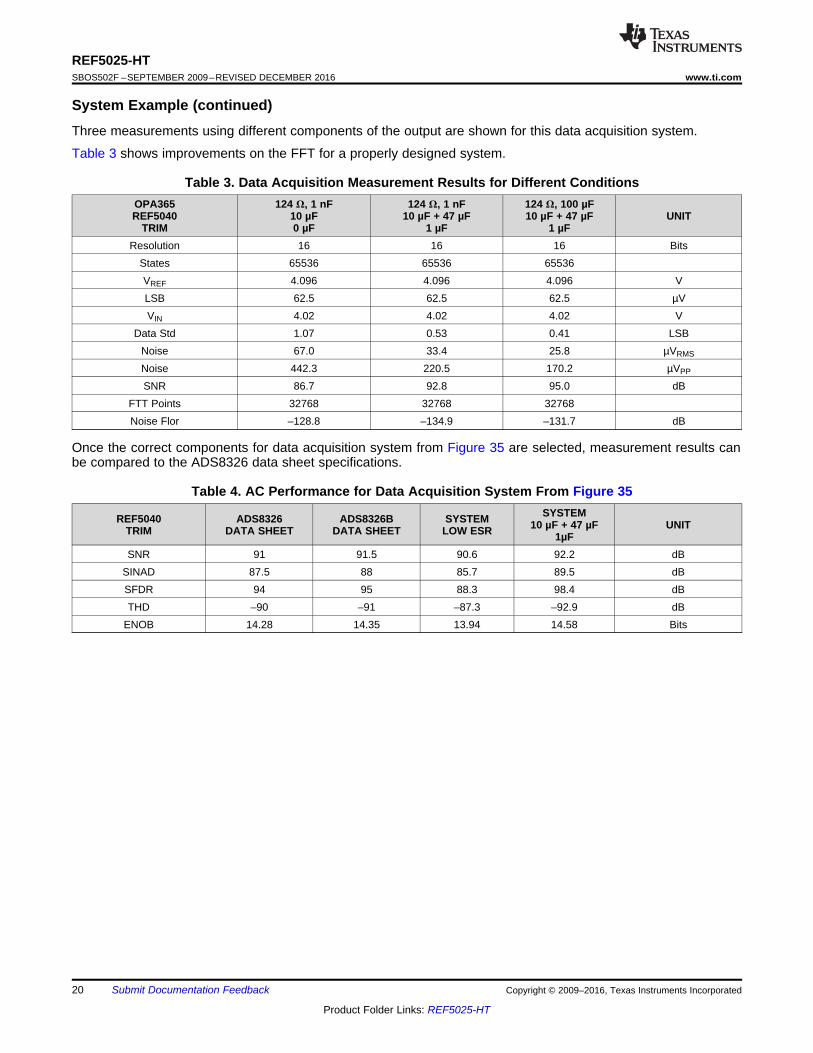
System Example (continued)Three measurements using different components of the output are shown for this data acquisition system.
Table 3 shows improvements on the FFT for a properly designed system.
Table 3. Data Acquisition Measurement Results for Different ConditionsOPA365REF5040
TRIM
124 Ω, 1 nF10 µF0 µF
124 Ω, 1 nF10 µF + 47 µF
1 µF
124 Ω, 100 µF10 µF + 47 µF
1 µFUNIT
Resolution 16 16 16 BitsStates 65536 65536 65536VREF 4.096 4.096 4.096 VLSB 62.5 62.5 62.5 µVVIN 4.02 4.02 4.02 V
Data Std 1.07 0.53 0.41 LSBNoise 67.0 33.4 25.8 µVRMS
Noise 442.3 220.5 170.2 µVPP
SNR 86.7 92.8 95.0 dBFTT Points 32768 32768 32768Noise Flor –128.8 –134.9 –131.7 dB
Once the correct components for data acquisition system from Figure 35 are selected, measurement results canbe compared to the ADS8326 data sheet specifications.
Table 4. AC Performance for Data Acquisition System From Figure 35
REF5040TRIM
ADS8326DATA SHEET
ADS8326BDATA SHEET
SYSTEMLOW ESR
SYSTEM10 µF + 47 µF
1µFUNIT
SNR 91 91.5 90.6 92.2 dBSINAD 87.5 88 85.7 89.5 dBSFDR 94 95 88.3 98.4 dBTHD –90 –91 –87.3 –92.9 dB
ENOB 14.28 14.35 13.94 14.58 Bits
DNC
TEMP VOUT
VIN
GND
DNC
NC
TRIM/NR
REF5025
CBYPASS
1 F to 10 Fm m
CL
1 F to 50 Fm m
+VSUPPLY
VOUT
Copyright © 2016, Texas Instruments Incorporated
21
REF5025-HTwww.ti.com SBOS502F –SEPTEMBER 2009–REVISED DECEMBER 2016
Product Folder Links: REF5025-HT
Submit Documentation FeedbackCopyright © 2009–2016, Texas Instruments Incorporated
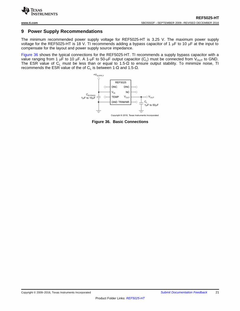
9 Power Supply RecommendationsThe minimum recommended power supply voltage for REF5025-HT is 3.25 V. The maximum power supplyvoltage for the REF5025-HT is 18 V. TI recommends adding a bypass capacitor of 1 μF to 10 μF at the input tocompensate for the layout and power supply source impedance.
Figure 36 shows the typical connections for the REF5025-HT. TI recommends a supply bypass capacitor with avalue ranging from 1 μF to 10 μF. A 1-μF to 50-μF output capacitor (CL) must be connected from VOUT to GND.The ESR value of CL must be less than or equal to 1.5-Ω to ensure output stability. To minimize noise, TIrecommends the ESR value of the of CL is between 1-Ω and 1.5-Ω.
Figure 36. Basic Connections
Low ESRCapacitor
ESR
VIH
TMP
GND
VOUT
Trim/NR
BypassCapacitor
NoiseReductionCapacitor
Low ESRCapacitor
VOUT
GND
22
REF5025-HTSBOS502F –SEPTEMBER 2009–REVISED DECEMBER 2016 www.ti.com
Product Folder Links: REF5025-HT
Submit Documentation Feedback Copyright © 2009–2016, Texas Instruments Incorporated
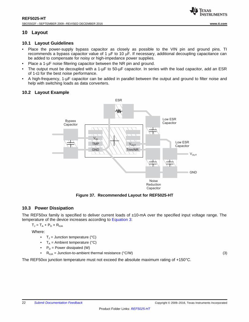
10 Layout
10.1 Layout Guidelines• Place the power-supply bypass capacitor as closely as possible to the VIN pin and ground pins. TI
recommends a bypass capacitor value of 1 μF to 10 μF. If necessary, additional decoupling capacitance canbe added to compensate for noisy or high-impedance power supplies.
• Place a 1-µF noise filtering capacitor between the NR pin and ground.• The output must be decoupled with a 1-µF to 50-µF capacitor. In series with the load capacitor, add an ESR
of 1-Ω for the best noise performance.• A high-frequency, 1-µF capacitor can be added in parallel between the output and ground to filter noise and
help with switching loads as data converters.
10.2 Layout Example
Figure 37. Recommended Layout for REF5025-HT
10.3 Power DissipationThe REF50xx family is specified to deliver current loads of ±10-mA over the specified input voltage range. Thetemperature of the device increases according to Equation 3:
TJ = TA + PD × RθJA
Where:• TJ = Junction temperature (°C)• TA = Ambient temperature (°C)• PD = Power dissipated (W)• RθJA = Junction-to-ambient thermal resistance (°C/W) (3)
The REF50xx junction temperature must not exceed the absolute maximum rating of +150°C.
23
REF5025-HTwww.ti.com SBOS502F –SEPTEMBER 2009–REVISED DECEMBER 2016
Product Folder Links: REF5025-HT
Submit Documentation FeedbackCopyright © 2009–2016, Texas Instruments Incorporated
11 Device and Documentation Support
11.1 Documentation Support
11.1.1 Related DocumentationFor related documentation see the following:• 0.05uV/degC (max), Single-Supply CMOS Zero-Drift Series Operational Amplifier (SBOS282)• REF5020 PSpice Model (SLIM160)• REF5020 TINA-TI Reference Design (SLIM159)• REF5020 TINA-TI Spice Model (SLIM158)• INA270 PSpice Model (SBOM485)• INA270 TINA-TI Reference Design (SBOC246)• INA270 TINA-TI Spice Model (SBOM306)• How a Voltage Reference Affects ADC Performance (SLYT331)
11.2 Receiving Notification of Documentation UpdatesTo receive notification of documentation updates, navigate to the device product folder on ti.com. In the upperright corner, click on Alert me to register and receive a weekly digest of any product information that haschanged. For change details, review the revision history included in any revised document.
11.3 Community ResourcesThe following links connect to TI community resources. Linked contents are provided "AS IS" by the respectivecontributors. They do not constitute TI specifications and do not necessarily reflect TI's views; see TI's Terms ofUse.
TI E2E™ Online Community TI's Engineer-to-Engineer (E2E) Community. Created to foster collaborationamong engineers. At e2e.ti.com, you can ask questions, share knowledge, explore ideas and helpsolve problems with fellow engineers.
Design Support TI's Design Support Quickly find helpful E2E forums along with design support tools andcontact information for technical support.
11.4 TrademarksE2E is a trademark of Texas Instruments.All other trademarks are the property of their respective owners.
11.5 Electrostatic Discharge CautionThese devices have limited built-in ESD protection. The leads should be shorted together or the device placed in conductive foamduring storage or handling to prevent electrostatic damage to the MOS gates.
11.6 GlossarySLYZ022 — TI Glossary.
This glossary lists and explains terms, acronyms, and definitions.
12 Mechanical, Packaging, and Orderable InformationThe following pages include mechanical, packaging, and orderable information. This information is the mostcurrent data available for the designated devices. This data is subject to change without notice and revision ofthis document. For browser-based versions of this data sheet, refer to the left-hand navigation.
PACKAGE OPTION ADDENDUM
www.ti.com 25-Oct-2016
Addendum-Page 1
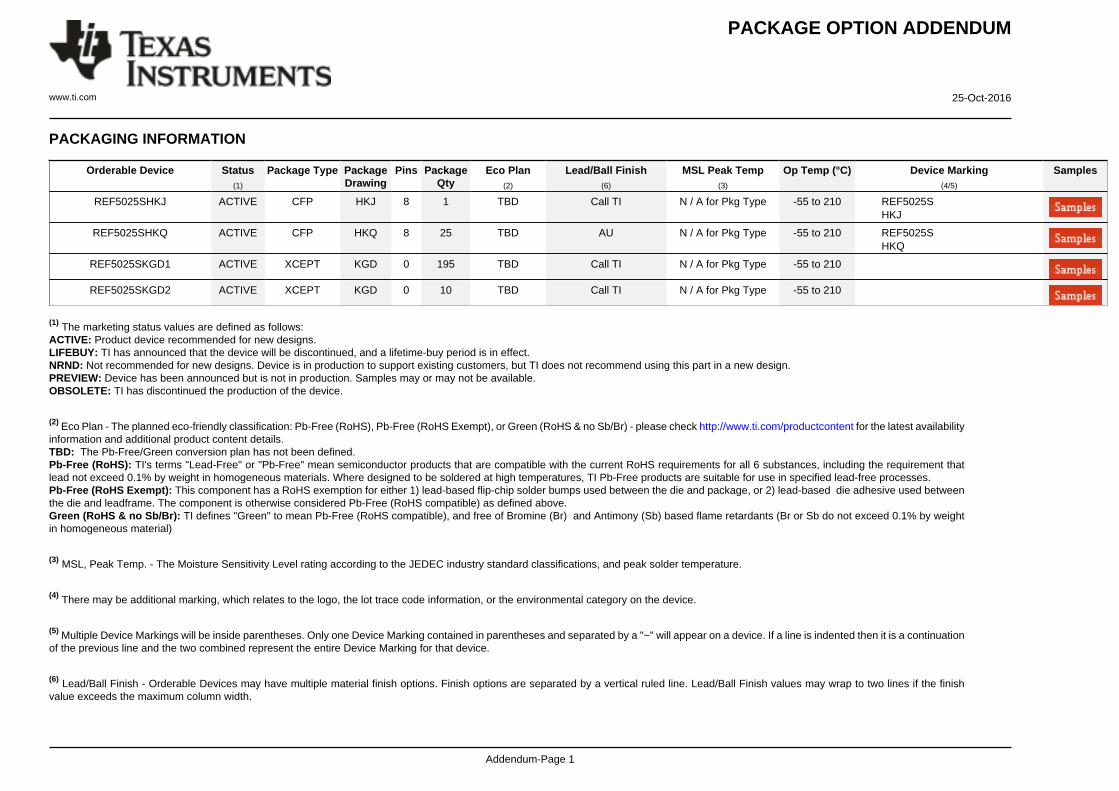
PACKAGING INFORMATION
Orderable Device Status(1)
Package Type PackageDrawing
Pins PackageQty
Eco Plan(2)
Lead/Ball Finish(6)
MSL Peak Temp(3)
Op Temp (°C) Device Marking(4/5)
Samples
REF5025SHKJ ACTIVE CFP HKJ 8 1 TBD Call TI N / A for Pkg Type -55 to 210 REF5025SHKJ
REF5025SHKQ ACTIVE CFP HKQ 8 25 TBD AU N / A for Pkg Type -55 to 210 REF5025SHKQ
REF5025SKGD1 ACTIVE XCEPT KGD 0 195 TBD Call TI N / A for Pkg Type -55 to 210
REF5025SKGD2 ACTIVE XCEPT KGD 0 10 TBD Call TI N / A for Pkg Type -55 to 210
(1) The marketing status values are defined as follows:ACTIVE: Product device recommended for new designs.LIFEBUY: TI has announced that the device will be discontinued, and a lifetime-buy period is in effect.NRND: Not recommended for new designs. Device is in production to support existing customers, but TI does not recommend using this part in a new design.PREVIEW: Device has been announced but is not in production. Samples may or may not be available.OBSOLETE: TI has discontinued the production of the device.
(2) Eco Plan - The planned eco-friendly classification: Pb-Free (RoHS), Pb-Free (RoHS Exempt), or Green (RoHS & no Sb/Br) - please check http://www.ti.com/productcontent for the latest availabilityinformation and additional product content details.TBD: The Pb-Free/Green conversion plan has not been defined.Pb-Free (RoHS): TI's terms "Lead-Free" or "Pb-Free" mean semiconductor products that are compatible with the current RoHS requirements for all 6 substances, including the requirement thatlead not exceed 0.1% by weight in homogeneous materials. Where designed to be soldered at high temperatures, TI Pb-Free products are suitable for use in specified lead-free processes.Pb-Free (RoHS Exempt): This component has a RoHS exemption for either 1) lead-based flip-chip solder bumps used between the die and package, or 2) lead-based die adhesive used betweenthe die and leadframe. The component is otherwise considered Pb-Free (RoHS compatible) as defined above.Green (RoHS & no Sb/Br): TI defines "Green" to mean Pb-Free (RoHS compatible), and free of Bromine (Br) and Antimony (Sb) based flame retardants (Br or Sb do not exceed 0.1% by weightin homogeneous material)
(3) MSL, Peak Temp. - The Moisture Sensitivity Level rating according to the JEDEC industry standard classifications, and peak solder temperature.
(4) There may be additional marking, which relates to the logo, the lot trace code information, or the environmental category on the device.
(5) Multiple Device Markings will be inside parentheses. Only one Device Marking contained in parentheses and separated by a "~" will appear on a device. If a line is indented then it is a continuationof the previous line and the two combined represent the entire Device Marking for that device.
(6) Lead/Ball Finish - Orderable Devices may have multiple material finish options. Finish options are separated by a vertical ruled line. Lead/Ball Finish values may wrap to two lines if the finishvalue exceeds the maximum column width.
PACKAGE OPTION ADDENDUM
www.ti.com 25-Oct-2016
Addendum-Page 2
Important Information and Disclaimer:The information provided on this page represents TI's knowledge and belief as of the date that it is provided. TI bases its knowledge and belief on informationprovided by third parties, and makes no representation or warranty as to the accuracy of such information. Efforts are underway to better integrate information from third parties. TI has taken andcontinues to take reasonable steps to provide representative and accurate information but may not have conducted destructive testing or chemical analysis on incoming materials and chemicals.TI and TI suppliers consider certain information to be proprietary, and thus CAS numbers and other limited information may not be available for release.
In no event shall TI's liability arising out of such information exceed the total purchase price of the TI part(s) at issue in this document sold by TI to Customer on an annual basis.
OTHER QUALIFIED VERSIONS OF REF5025-HT :
• Catalog: REF5025
• Enhanced Product: REF5025-EP
NOTE: Qualified Version Definitions:
• Catalog - TI's standard catalog product
• Enhanced Product - Supports Defense, Aerospace and Medical Applications
IMPORTANT NOTICE
Texas Instruments Incorporated and its subsidiaries (TI) reserve the right to make corrections, enhancements, improvements and otherchanges to its semiconductor products and services per JESD46, latest issue, and to discontinue any product or service per JESD48, latestissue. Buyers should obtain the latest relevant information before placing orders and should verify that such information is current andcomplete. All semiconductor products (also referred to herein as “components”) are sold subject to TI’s terms and conditions of salesupplied at the time of order acknowledgment.TI warrants performance of its components to the specifications applicable at the time of sale, in accordance with the warranty in TI’s termsand conditions of sale of semiconductor products. Testing and other quality control techniques are used to the extent TI deems necessaryto support this warranty. Except where mandated by applicable law, testing of all parameters of each component is not necessarilyperformed.TI assumes no liability for applications assistance or the design of Buyers’ products. Buyers are responsible for their products andapplications using TI components. To minimize the risks associated with Buyers’ products and applications, Buyers should provideadequate design and operating safeguards.TI does not warrant or represent that any license, either express or implied, is granted under any patent right, copyright, mask work right, orother intellectual property right relating to any combination, machine, or process in which TI components or services are used. Informationpublished by TI regarding third-party products or services does not constitute a license to use such products or services or a warranty orendorsement thereof. Use of such information may require a license from a third party under the patents or other intellectual property of thethird party, or a license from TI under the patents or other intellectual property of TI.Reproduction of significant portions of TI information in TI data books or data sheets is permissible only if reproduction is without alterationand is accompanied by all associated warranties, conditions, limitations, and notices. TI is not responsible or liable for such altereddocumentation. Information of third parties may be subject to additional restrictions.Resale of TI components or services with statements different from or beyond the parameters stated by TI for that component or servicevoids all express and any implied warranties for the associated TI component or service and is an unfair and deceptive business practice.TI is not responsible or liable for any such statements.Buyer acknowledges and agrees that it is solely responsible for compliance with all legal, regulatory and safety-related requirementsconcerning its products, and any use of TI components in its applications, notwithstanding any applications-related information or supportthat may be provided by TI. Buyer represents and agrees that it has all the necessary expertise to create and implement safeguards whichanticipate dangerous consequences of failures, monitor failures and their consequences, lessen the likelihood of failures that might causeharm and take appropriate remedial actions. Buyer will fully indemnify TI and its representatives against any damages arising out of the useof any TI components in safety-critical applications.In some cases, TI components may be promoted specifically to facilitate safety-related applications. With such components, TI’s goal is tohelp enable customers to design and create their own end-product solutions that meet applicable functional safety standards andrequirements. Nonetheless, such components are subject to these terms.No TI components are authorized for use in FDA Class III (or similar life-critical medical equipment) unless authorized officers of the partieshave executed a special agreement specifically governing such use.Only those TI components which TI has specifically designated as military grade or “enhanced plastic” are designed and intended for use inmilitary/aerospace applications or environments. Buyer acknowledges and agrees that any military or aerospace use of TI componentswhich have not been so designated is solely at the Buyer's risk, and that Buyer is solely responsible for compliance with all legal andregulatory requirements in connection with such use.TI has specifically designated certain components as meeting ISO/TS16949 requirements, mainly for automotive use. In any case of use ofnon-designated products, TI will not be responsible for any failure to meet ISO/TS16949.
Products ApplicationsAudio www.ti.com/audio Automotive and Transportation www.ti.com/automotiveAmplifiers amplifier.ti.com Communications and Telecom www.ti.com/communicationsData Converters dataconverter.ti.com Computers and Peripherals www.ti.com/computersDLP® Products www.dlp.com Consumer Electronics www.ti.com/consumer-appsDSP dsp.ti.com Energy and Lighting www.ti.com/energyClocks and Timers www.ti.com/clocks Industrial www.ti.com/industrialInterface interface.ti.com Medical www.ti.com/medicalLogic logic.ti.com Security www.ti.com/securityPower Mgmt power.ti.com Space, Avionics and Defense www.ti.com/space-avionics-defenseMicrocontrollers microcontroller.ti.com Video and Imaging www.ti.com/videoRFID www.ti-rfid.comOMAP Applications Processors www.ti.com/omap TI E2E Community e2e.ti.comWireless Connectivity www.ti.com/wirelessconnectivity
Mailing Address: Texas Instruments, Post Office Box 655303, Dallas, Texas 75265Copyright © 2016, Texas Instruments Incorporated