Embed Size (px)
Citation preview
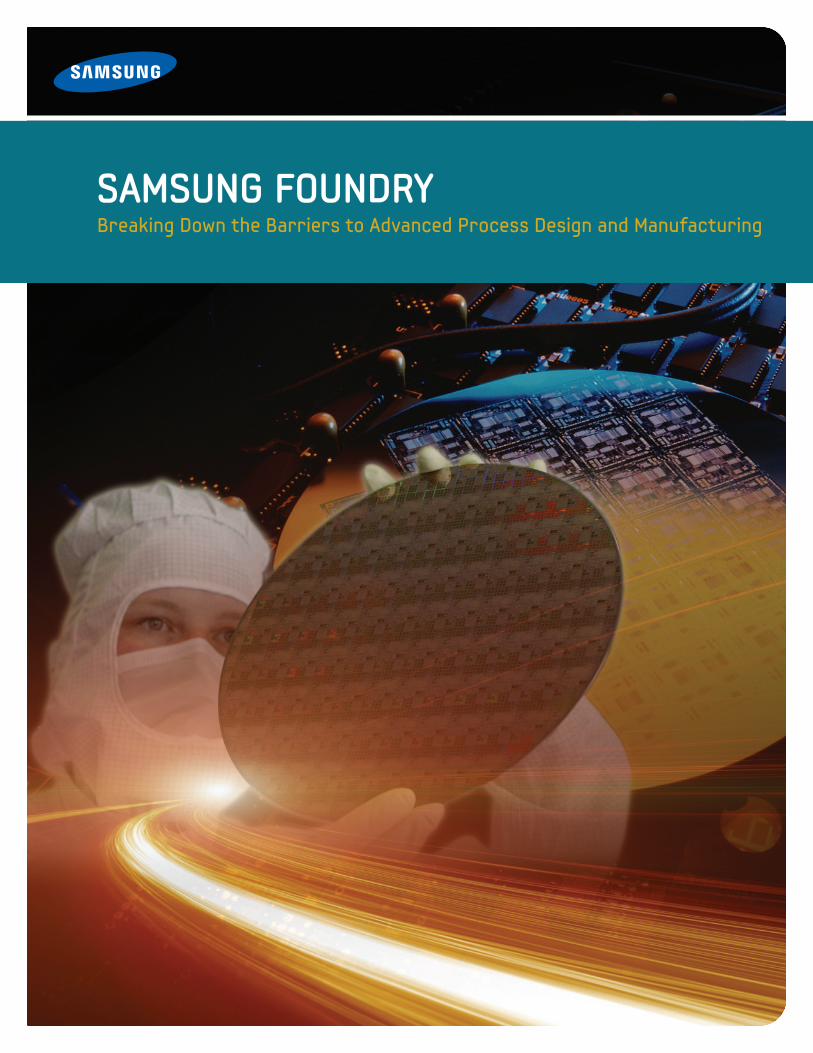
SAMSUNG FOUNDRYBreaking Down the Barriers to Advanced Process Design and Manufacturing
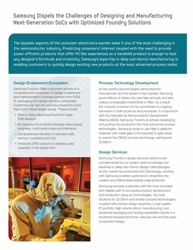
Design Enablement Ecosystem Samsung Foundry offers customers access to a comprehensive ecosystem of design enablement and implementation business partners from EDA, IP, packaging and design services companies. Customers can tap into services required to solve their most critical design issues. These include:
• Best-in-class reference flows from major EDA vendors
• An extensive IP portfolio including mixed signal, periphera, multimedia cores and interfaces
• Comprehensive libraries of standard cells, memory compilers and I/Os
• Predictive DFM solutions to address yield upstream in the design flow
Process Technology Development
As the world’s second-largest semiconductor manufacturer and the leader in key markets, Samsung pours billions of dollars into new fabs annually and also makes considerable investments in R&D. As a result, the company is known for its commitment to ongoing innovation in both products and processes. In conjunction with the International Semiconductor Development Alliance (ISDA), Samsung Foundry is actively developing and putting into production the most advanced process technologies. Samsung chose to use High-k dielectric materials with metal gate in the transistor’s gate stack to extend the CMOS process technology well beyond 32/28nm.
Design Services
Samsung Foundry’s design services solutions are complemented by our system-level knowledge and expertise in deep sub-micron design methodologies. As the market has embraced SoC technology, working with Samsung enables customers to streamline the creation and differentiate leading-edge products.
Samsung provides customers with the most complete and reliable path to successful product development and production using our technologies. Our total solutions for 32/28nm and smaller process technologies, coupled with premier design expertise, a high-quality IP portfolio, high-volume silicon manufacturing, and advanced packaging and testing capabilities results in a shortened development time, reduced risk and first-pass component design.
The dynamic aspects of the consumer electronics market make it one of the most challenging in the semiconductor industry. Predicting consumers’ interest coupled with the need to provide power efficient products that offer PC-like experiences on a handheld product is enough to test any designer’s fortitude and creativity. Samsung’s expertise in deep sub-micron manufacturing is enabling customers to quickly design exciting new products at the most advanced process nodes.
Samsung Dispels the Challenges of Designing and Manufacturing Next-Generation SoCs with Optimized Foundry Solutions
• Advanced Process Technology
In addition to its own significant process R&D investments, Samsung is actively involved in many joint research and development alliances, including ISDA. As a result, Samsung foundry customers can design innovative products built on the most advanced process platforms.
•Design IP
Samsung has an extensive portfolio of libraries and IP that is available to customers, particularly in the CPU, embedded memory and mixed signal areas, including licensed IP from leading companies such as ARM®, Snowbush®, and Synopsys®.
•ManufacturingPlant
Maintains advanced 90, 65, 45, 32/28nm production equipment. The Giheung, South Korea foundry serves customers with leading-edge, high-volume manufacturing services.
•PartnershipsforMulti-sourcing
Along with IBM and GLOBALFOUNDRIES, Samsung is a member of the Common Platform alliance. The three companies provide worldwide multi-sourcing of the same product design to meet customer needs, without any redesign required.
•ExtensiveCustomerSupport
From the initial engagement to volume manufacturing, Samsung’s business, engineering and logistics teams are focused on full customer satisfaction.
•CustomerIPProtection
Samsung has put firewalls and strict security systems in place to ensure that no unauthorized individuals have any access to customer IP. Customers can audit the system at any time.
•Long-termCommitment
Samsung has made the investments in facilities, personnel and time in order for its foundry to succeed over the long term. The company’s executive-level commitment and financial strength are the backbone enabling this approach.
“With three world-class manufacturing facilities currently online, Samsung Foundry is focused on providing advanced logic technology and is able to meet customer demand for high-performance, low-power chips.” -Ana Hunter, vice president of Foundry, Samsung Semiconductor, Inc.
Unequaled Customer Benefits
© 2012. The appearance of all products, dates, figures, diagrams and tables are subject to change at any time without notice. Samsung and Samsung Semiconduc-tor, Inc. are trademarks of Samsung Electronics Co., Ltd.
BRO-12-FOUNDRY-001 Printed 03/12
Samsung Semiconductor, Inc.
3655 North First St., San Jose, CA 95134-1713 TEL: 408-544-4000 FAX: 408-544-4950
A Closer Look—Samsung Foundry’s Offerings
The fab is located on a 350-acre site in Giheung, South Korea. It has a round-the-clock staff that includes dedicated resources for customer service, design, DFM, product engineering, test, failure analysis and reliability.
For more information, visit Samsung Foundry at: www.samsung.com/us/business/foundry Join the conversation! Samsung’s blog at: www.voicesatsamsungsemiconductor.com Or at our Samsung Facebook page at: www.facebook.com/Samsung/USATech
Advanced Process Technologies
• 65nm
• 45nm
• 32/28nm HKMG
• 20nm HKMG*
*Targeted for 2H 2012
AMBA-based Peripherals
• AMBA-2.0/3.0-based Peripherals
• Memory Controller (SDRAM/SRAM/NOR/NAND)
• Multimedia Card Interface (SDMMC/SDIO)
• ARM Prime Cell
CPU Cores
• ARM Cortex A9/A15
• ARM 7, 9 & 11 families
• Cortex-M Series
DSP Cores
• TeakLite
• Teak
General & Special-purpose I/O
• LVCMOS (In-Line, STG, CUP)
• SSTL2/SSTL18/SSTL15/SSTL12
High-Speed Interfaces (Link)
• USB HS OTG/Device/Host
• S-ATA
• 10/100/1000M Ethernet
• UniPro
• PCI Device/Bridge
High-Speed Interfaces (PHY)
• USB 2.0/ USB 3.0
• 8G Universal SerDes (SAS/SATA/PCI Express)
• 3G/6G Serial ATA
• DDR2, DDR3, mDDR, LPDDR2
• DDR3/2 combo
• LVDS, subLVDS, mini-LVDS
• HDMI
• Display Port
• MIPI
Memories
• Single-Port SRAM (HD, LP)
• Dual-Port SRAM (HD, LP)
• Register File (1RW, 1R1W)
• Redundancy SRAM
• ROM (Via)
• OTP
Mixed-Signal Cores
• ADC: 6 to 14 bits, up to 450MHz
• DAC: 8 to 16 bits, up to 300MHz
• PLL: Up to 2GHz, Frequency Synthesizer, De-skew, Pixel Clock, Dithered, Clock
• CODEC: 16-bit Audio, 14-bit Voice
• AFE
• Voltage Regulator
Multimedia
• MPEG4/H.264
• 2D/3D Engine
• JPEG Codec
• NTSC/PAL Encoder
Peripheral Cores
• 10/100 MAC Ethernet Controllers
• USB 2.0/3.0 Function Cores
• EEE 1394 Link Controllers
• PCIe Controllers
• SATA Controllers
• IrDA
• UART
• Synchronous Serial I/F
• Real-Time Clocks
• Keyboard/Mouse I/F
• General-purpose I/F
• Smart Card/SIM I/F
• Multimedia Card I/F
• Asynchronous Static Memory Controllers (SRAM, Flash, ROM)
• Universal Memory Controllers (SDRAM, Synch Flash, SRAM)
• DMA Controllers
• LCD Controllers
• Watch-dog Timers
• Programmable Interrupt Controllers
Standard Cell Library
• High Density
• High Speed
• Multi VT
• Power Management Kit
• Multi Channel