Embed Size (px)
Citation preview
An IMPORTANT NOTICE at the end of this TI reference design addresses authorized use, intellectual property matters and other important disclaimers and information.
TINA-TI is a trademark of Texas Instruments WEBENCH is a registered trademark of Texas Instruments
TIDU022-July 2015 Sample & Hold Glitch Reduction for Precision Outputs 1 Copyright © 2015, Texas Instruments Incorporated
Matthew Sauceda
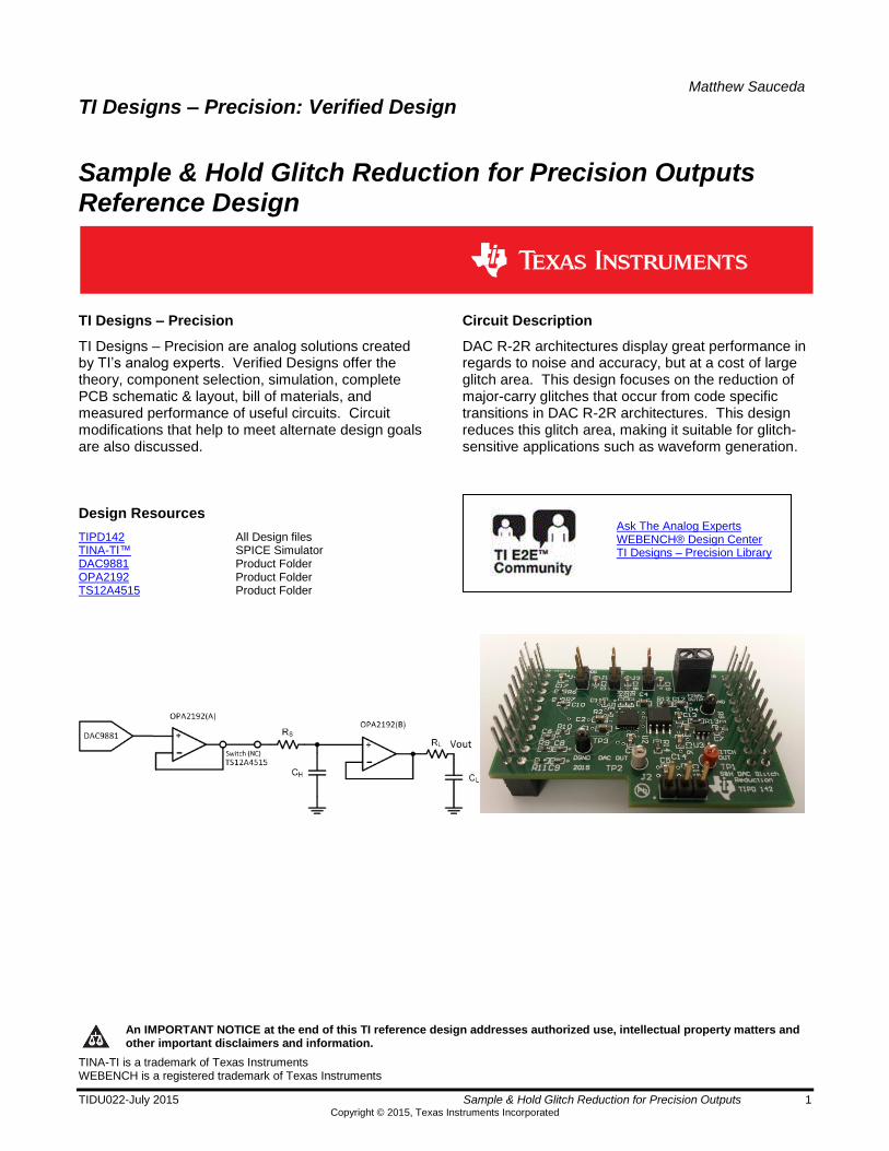
TI Designs – Precision: Verified Design
Sample & Hold Glitch Reduction for Precision Outputs Reference Design
TI Designs – Precision Circuit Description
TI Designs – Precision are analog solutions created by TI’s analog experts. Verified Designs offer the theory, component selection, simulation, complete PCB schematic & layout, bill of materials, and measured performance of useful circuits. Circuit modifications that help to meet alternate design goals are also discussed.
DAC R-2R architectures display great performance in regards to noise and accuracy, but at a cost of large glitch area. This design focuses on the reduction of major-carry glitches that occur from code specific transitions in DAC R-2R architectures. This design reduces this glitch area, making it suitable for glitch-sensitive applications such as waveform generation.
Design Resources
TIPD142 All Design files TINA-TI™ SPICE Simulator DAC9881 Product Folder OPA2192 Product Folder TS12A4515 Product Folder
Ask The Analog Experts WEBENCH® Design Center TI Designs – Precision Library
www.ti.com
2 Sample & Hold Glitch Reduction for Precision Outputs TIDU022-July 2015 Copyright © 2015, Texas Instruments Incorporated
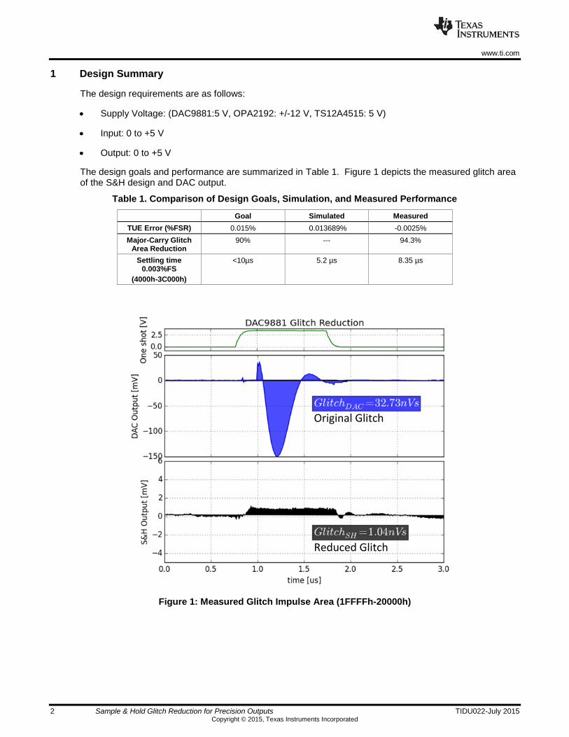
1 Design Summary
The design requirements are as follows:
Supply Voltage: (DAC9881:5 V, OPA2192: +/-12 V, TS12A4515: 5 V)
Input: 0 to +5 V
Output: 0 to +5 V
The design goals and performance are summarized in Table 1. Figure 1 depicts the measured glitch area of the S&H design and DAC output.
Table 1. Comparison of Design Goals, Simulation, and Measured Performance
Goal Simulated Measured
TUE Error (%FSR) 0.015% 0.013689% -0.0025%
Major-Carry Glitch Area Reduction
90% --- 94.3%
Settling time 0.003%FS
(4000h-3C000h)
<10µs 5.2 µs 8.35 µs
Original Glitch
Reduced Glitch
Figure 1: Measured Glitch Impulse Area (1FFFFh-20000h)
www.ti.com
TIDU022-July 2015 Sample & Hold Glitch Reduction for Precision Outputs 3 Copyright © 2015, Texas Instruments Incorporated
2 Theory of Operation
2.1 DAC Glitch Energy
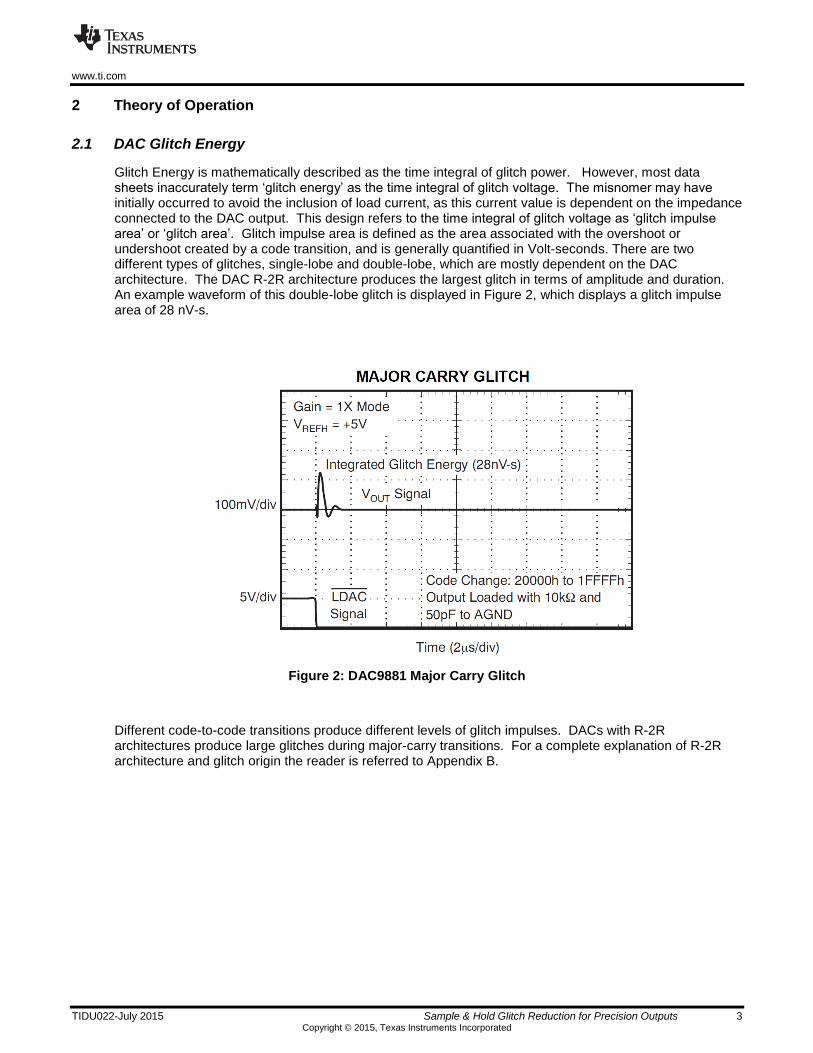
Glitch Energy is mathematically described as the time integral of glitch power. However, most data sheets inaccurately term ‘glitch energy’ as the time integral of glitch voltage. The misnomer may have initially occurred to avoid the inclusion of load current, as this current value is dependent on the impedance connected to the DAC output. This design refers to the time integral of glitch voltage as ‘glitch impulse area’ or ‘glitch area’. Glitch impulse area is defined as the area associated with the overshoot or undershoot created by a code transition, and is generally quantified in Volt-seconds. There are two different types of glitches, single-lobe and double-lobe, which are mostly dependent on the DAC architecture. The DAC R-2R architecture produces the largest glitch in terms of amplitude and duration. An example waveform of this double-lobe glitch is displayed in Figure 2, which displays a glitch impulse area of 28 nV-s.
Figure 2: DAC9881 Major Carry Glitch
Different code-to-code transitions produce different levels of glitch impulses. DACs with R-2R architectures produce large glitches during major-carry transitions. For a complete explanation of R-2R architecture and glitch origin the reader is referred to Appendix B.
www.ti.com
4 Sample & Hold Glitch Reduction for Precision Outputs TIDU022-July 2015 Copyright © 2015, Texas Instruments Incorporated
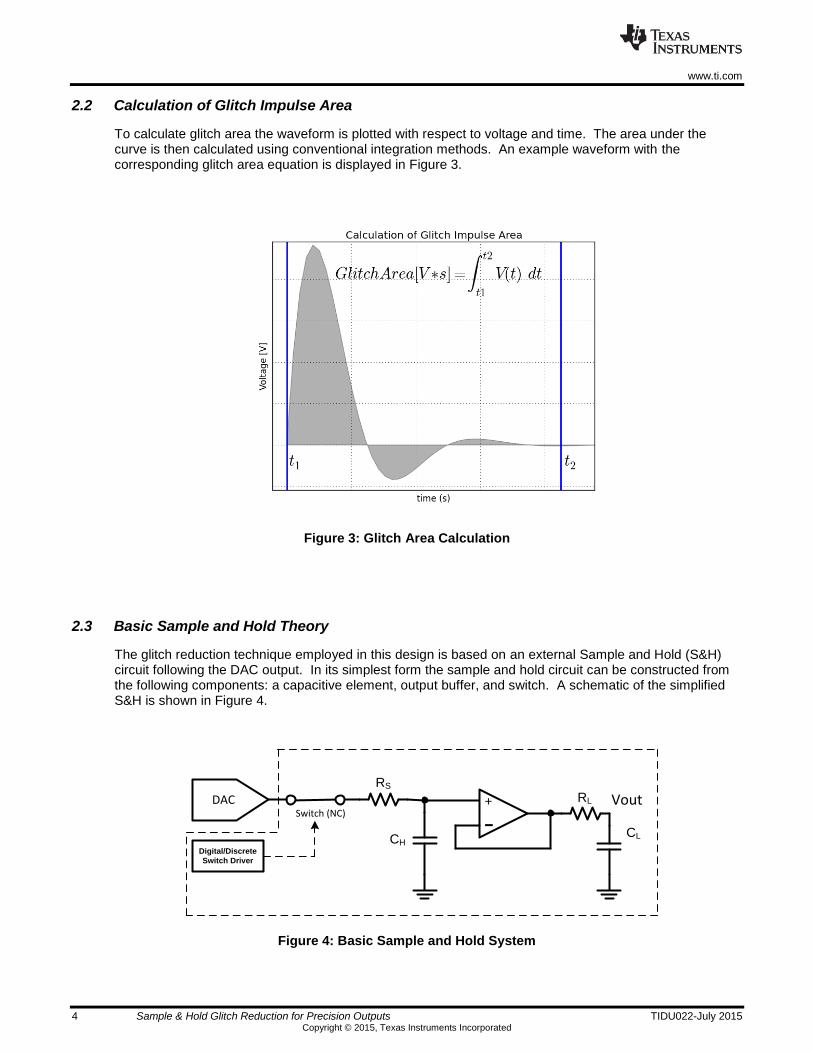
2.2 Calculation of Glitch Impulse Area
To calculate glitch area the waveform is plotted with respect to voltage and time. The area under the curve is then calculated using conventional integration methods. An example waveform with the corresponding glitch area equation is displayed in Figure 3.
Figure 3: Glitch Area Calculation
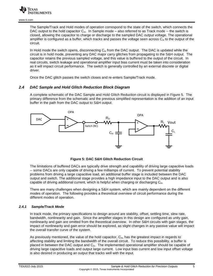
2.3 Basic Sample and Hold Theory
The glitch reduction technique employed in this design is based on an external Sample and Hold (S&H) circuit following the DAC output. In its simplest form the sample and hold circuit can be constructed from the following components: a capacitive element, output buffer, and switch. A schematic of the simplified S&H is shown in Figure 4.
RS
CH
+ RL
CL
Switch (NC)VoutDAC
Digital/Discrete
Switch Driver
Figure 4: Basic Sample and Hold System
www.ti.com
TIDU022-July 2015 Sample & Hold Glitch Reduction for Precision Outputs 5 Copyright © 2015, Texas Instruments Incorporated
The Sample/Track and Hold modes of operation correspond to the state of the switch, which connects the DAC output to the hold capacitor CH. In Sample mode – also referred to as Track mode -- the switch is closed, allowing the capacitor to charge or discharge to the sampled DAC output voltage. The operational amplifier is configured as a buffer, which tracks and passes the voltage seen across CH to the output of the circuit.
In Hold mode the switch opens, disconnecting CH from the DAC output. The DAC is updated while the circuit is in hold mode, preventing any DAC major carry glitches from propagating to the S&H output. The capacitor retains the previous sampled voltage, and this value is buffered to the output of the circuit. In real circuits, switch leakage and operational amplifier input bias current must be taken into consideration as it will impact circuit performance. The switch is generally controlled by an external discrete or digital driver.
Once the DAC glitch passes the switch closes and re-enters Sample/Track mode.
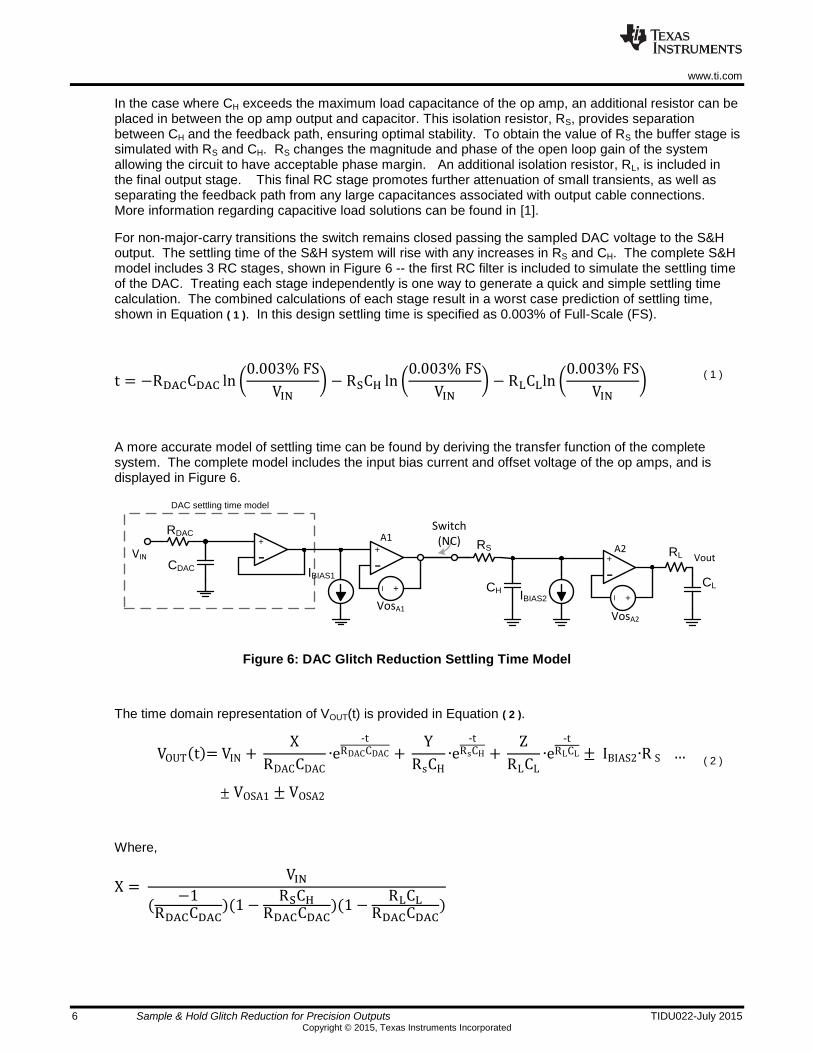
2.4 DAC Sample and Hold Glitch Reduction Block Diagram
A complete schematic of the DAC Sample and Hold Glitch Reduction circuit is displayed in Figure 5. The primary difference from the schematic and the previous simplified representation is the addition of an input buffer in the path from the DAC output to S&H output.
RS
CH
+ RL
CL
Switch (NC)
+Vout
DAC
OPAOPA
Figure 5: DAC S&H Glitch Reduction Circuit
The limitations of buffered DACs are typically drive strength and capability of driving large capacitive loads -- some DACs are only capable of driving a few milliamps of current. To prevent potential stability problems from driving a large capacitive load, an additional buffer stage is included between the DAC output and switch. The additional stage provides a high impedance input to the DAC output and is also capable of driving additional current, which is helpful when charging or discharging CH.
There are many challenges when designing a S&H system, which are mainly dependent on the different modes of operation. The following provides a theoretical overview of circuit performance during the different modes of operation.
2.4.1 Sample/Track Mode
In track mode, the primary specifications to design around are stability, offset, settling time, slew rate, bandwidth, nonlinearity and gain. Since the amplifier stages in this design are configured as unity gain, nonlinearity and gain are omitted from the theoretical overview. In other S&H circuits with gain stages, the impact of nonlinearity and gain error should be explored, as slight changes in any passive value will impact the overall transfer curve of the system.
As previously mentioned, the value of the hold capacitor, CH, has the greatest impact in regards to affecting stability and limiting the bandwidth of the overall circuit. To reduce this possibility, a buffer is placed in between the DAC output and CH. The implemented operational amplifier should be capable of driving large capacitive loads and output large current. Low input bias current and low input offset voltage is also desired in producing an output that tracks well with the input.
www.ti.com
6 Sample & Hold Glitch Reduction for Precision Outputs TIDU022-July 2015 Copyright © 2015, Texas Instruments Incorporated
In the case where CH exceeds the maximum load capacitance of the op amp, an additional resistor can be placed in between the op amp output and capacitor. This isolation resistor, RS, provides separation between CH and the feedback path, ensuring optimal stability. To obtain the value of RS the buffer stage is simulated with RS and CH. RS changes the magnitude and phase of the open loop gain of the system allowing the circuit to have acceptable phase margin. An additional isolation resistor, RL, is included in the final output stage. This final RC stage promotes further attenuation of small transients, as well as separating the feedback path from any large capacitances associated with output cable connections. More information regarding capacitive load solutions can be found in [1].
For non-major-carry transitions the switch remains closed passing the sampled DAC voltage to the S&H output. The settling time of the S&H system will rise with any increases in RS and CH. The complete S&H model includes 3 RC stages, shown in Figure 6 -- the first RC filter is included to simulate the settling time of the DAC. Treating each stage independently is one way to generate a quick and simple settling time calculation. The combined calculations of each stage result in a worst case prediction of settling time, shown in Equation ( 1 ). In this design settling time is specified as 0.003% of Full-Scale (FS).
t = −RDACCDAC ln (0.003% FS
VIN) − RSCH ln (
0.003% FS
VIN) − RLCLln (
0.003% FS
VIN) ( 1 )
A more accurate model of settling time can be found by deriving the transfer function of the complete system. The complete model includes the input bias current and offset voltage of the op amps, and is displayed in Figure 6.
RDAC+
CDAC
RS
CH
+RL
CL
IBIAS2
Switch (NC)
+
IBIAS1
DAC settling time model
VIN Vout
A1A2
+–
VosA1VosA2
+–
Figure 6: DAC Glitch Reduction Settling Time Model
The time domain representation of VOUT(t) is provided in Equation ( 2 ).
VOUT(t)= VIN + X
RDACCDAC∙e
-tRDACCDAC +
Y
RsCH∙e
-tRsCH +
Z
RLCL∙e
-tRLCL ± IBIAS2∙R S …
± VOSA1 ± VOSA2
( 2 )
Where,
X = VIN
(−1
RDACCDAC)(1 −
RSCH
RDACCDAC)(1 −
RLCL
RDACCDAC)
www.ti.com
TIDU022-July 2015 Sample & Hold Glitch Reduction for Precision Outputs 7 Copyright © 2015, Texas Instruments Incorporated
Y = VIN
(−1
RsCH)(1 −
RDACCDAC
RSCH)(1 −
RLCL
RSCH)
Z = VIN
(−1
RLCL) (1 −
RDACCDAC
RLCL) (1 −
RSCH
RLCL)
The derivation of this Equation is provided in Appendix C.
RDAC and CDAC are back calculated using the settling time parameter in the DAC’s datasheet. The RC calculation is derived from the simple first order RC discharge model.
RDACCDAC =−t
ln (0.003% FS
VIN) ( 3 )
Another parameter that may impact settling time is the on-resistance of the solid state switch, RON. An illustration of this additional series resistance is provided in Figure 7. To update the previous formula, the switch on-resistance, RON, is linearly added to RS, creating a new equivalent resistance value RS’ -- (RS’ = RS + RON).
RS
Switch (NC)
RSRON
Figure 7: Switch on-resistance
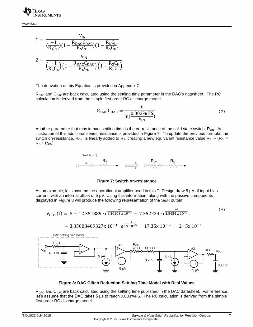
As an example, let’s assume the operational amplifier used in this TI Design draw 5 pA of input bias current, with an internal offset of 5 µV. Using this information, along with the passive components displayed in Figure 8 will produce the following representation of the S&H output.
VOUT(t) = 5 − 12.351889 ∙ e−t
4.80108 x 10⁻⁷ + 7.352224 ∙ e−t
2.8454 x 10⁻⁷ … ( 4 )
− 3.35008409327x 10⁻⁴ ∙ e−t
3 x 10⁻⁹ ± 17.35x 10⁻¹¹ ± 2 ∙ 5x 10⁻⁶
10 Ω +
48.1 nF ++
5 pA
DAC settling time model
VIN Vout
A1A2
+–
+–
RON
20 Ω 14.7 Ω
8.2 nF5 pA
5 µV
10 Ω
300 pF
5 µV
Figure 8: DAC Glitch Reduction Settling Time Model with Real Values
RDAC and CDAC are back calculated using the settling time published in the DAC datasheet. For reference, let’s assume that the DAC takes 5 µs to reach 0.003%FS. The RC calculation is derived from the simple first order RC discharge model.
www.ti.com
8 Sample & Hold Glitch Reduction for Precision Outputs TIDU022-July 2015 Copyright © 2015, Texas Instruments Incorporated
RDACCDAC =−t
ln (0.003% FS
VIN)
= −5μs
ln (0.00015V
5V)
= 4.80108 x 10⁻⁷ΩF ( 5 )
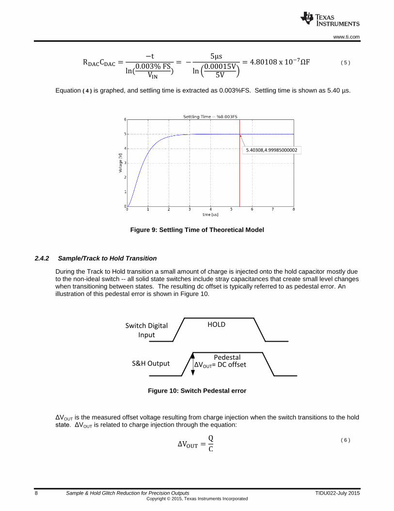
Equation ( 4 ) is graphed, and settling time is extracted as 0.003%FS. Settling time is shown as 5.40 µs.
5.40308,4.99985000002
Figure 9: Settling Time of Theoretical Model
2.4.2 Sample/Track to Hold Transition
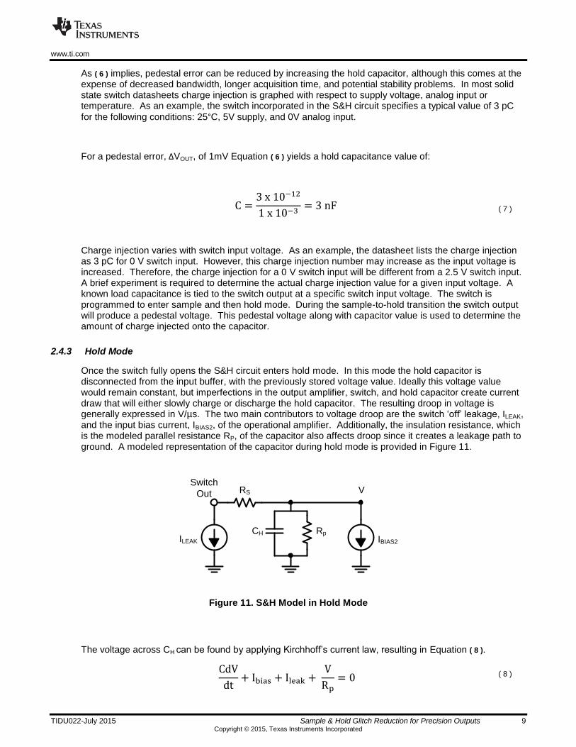
During the Track to Hold transition a small amount of charge is injected onto the hold capacitor mostly due to the non-ideal switch -- all solid state switches include stray capacitances that create small level changes when transitioning between states. The resulting dc offset is typically referred to as pedestal error. An illustration of this pedestal error is shown in Figure 10.
S&H Output
Switch Digital Input
Pedestal
HOLD
ΔVOUT= DC offset
Figure 10: Switch Pedestal error
ΔVOUT is the measured offset voltage resulting from charge injection when the switch transitions to the hold state. ΔVOUT is related to charge injection through the equation:
∆VOUT =Q
C
( 6 )
www.ti.com
TIDU022-July 2015 Sample & Hold Glitch Reduction for Precision Outputs 9 Copyright © 2015, Texas Instruments Incorporated
As ( 6 ) implies, pedestal error can be reduced by increasing the hold capacitor, although this comes at the expense of decreased bandwidth, longer acquisition time, and potential stability problems. In most solid state switch datasheets charge injection is graphed with respect to supply voltage, analog input or temperature. As an example, the switch incorporated in the S&H circuit specifies a typical value of 3 pC
for the following conditions: 25°C, 5V supply, and 0V analog input.
For a pedestal error, ΔVOUT, of 1mV Equation ( 6 ) yields a hold capacitance value of:
C =3 x 10⁻¹²
1 x 10−3= 3 nF
( 7 )
Charge injection varies with switch input voltage. As an example, the datasheet lists the charge injection as 3 pC for 0 V switch input. However, this charge injection number may increase as the input voltage is increased. Therefore, the charge injection for a 0 V switch input will be different from a 2.5 V switch input. A brief experiment is required to determine the actual charge injection value for a given input voltage. A known load capacitance is tied to the switch output at a specific switch input voltage. The switch is programmed to enter sample and then hold mode. During the sample-to-hold transition the switch output will produce a pedestal voltage. This pedestal voltage along with capacitor value is used to determine the amount of charge injected onto the capacitor.
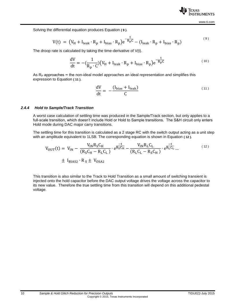
2.4.3 Hold Mode
Once the switch fully opens the S&H circuit enters hold mode. In this mode the hold capacitor is disconnected from the input buffer, with the previously stored voltage value. Ideally this voltage value would remain constant, but imperfections in the output amplifier, switch, and hold capacitor create current draw that will either slowly charge or discharge the hold capacitor. The resulting droop in voltage is generally expressed in V/µs. The two main contributors to voltage droop are the switch ‘off’ leakage, ILEAK, and the input bias current, IBIAS2, of the operational amplifier. Additionally, the insulation resistance, which is the modeled parallel resistance RP, of the capacitor also affects droop since it creates a leakage path to ground. A modeled representation of the capacitor during hold mode is provided in Figure 11.
RS
ILEAK IBIAS2
Rp
VSwitch
Out
CH
Figure 11. S&H Model in Hold Mode
The voltage across CH can be found by applying Kirchhoff’s current law, resulting in Equation ( 8 ).
CdV
dt+ Ibias + Ileak +
V
Rp= 0
( 8 )
www.ti.com
10 Sample & Hold Glitch Reduction for Precision Outputs TIDU022-July 2015 Copyright © 2015, Texas Instruments Incorporated
Solving the differential equation produces Equation ( 9 ).
V(t) = (VH + Ileak ∙ Rp + Ibias ∙ Rp)e−
tRpC − (Ileak ∙ Rp + Ibias ∙ Rp)
( 9 )
The droop rate is calculated by taking the time-derivative of V(t).
dV
dt= −(
1
Rp ∙ C)(VH + Ileak ∙ Rp + Ibias ∙ Rp)e
−t
RpC ( 10 )
As RP approaches ∞ the non-ideal model approaches an ideal representation and simplifies this expression to Equation ( 11 ).
dV
dt= −
(Ibias + Ileak)
C
( 11 )
2.4.4 Hold to Sample/Track Transition
A worst case calculation of settling time was produced in the Sample/Track section, but only applies to a full-scale transition, which doesn’t include Hold or Hold to Sample transitions. The S&H circuit only enters Hold mode during DAC major carry transitions.
The settling time for this transition is calculated as a 2 stage RC with the switch output acting as a unit step with an amplitude equivalent to 1LSB. The corresponding equation is shown in Equation ( 12 ).
VOUT(t) = VIN − VINRSCH
(RSCH − RLCL )∙ e
−tRSCH −
VINRLCL
(RLCL − RSCH )∙ e
−tRLCL …
( 12 )
± IBIAS2 ∙ R S ± VOSA2
This transition is also similar to the Track to Hold Transition as a small amount of switching transient is injected onto the hold capacitor before the DAC output voltage drives the voltage across the capacitor to its new value. Therefore the true settling time from this transition will depend on this additional pedestal voltage.
www.ti.com
TIDU022-July 2015 Sample & Hold Glitch Reduction for Precision Outputs 11 Copyright © 2015, Texas Instruments Incorporated
3 Component Selection
3.1 DAC Selection
DAC selection for this design is based on glitch performance, resolution, and end-use in precision instrumentation and automatic test equipment where minimal glitch energies are necessary in maintaining performance.
The DAC9881 is a single-channel device offering 18 bits or resolution, with fast settling time and an on-chip precision output amplifier. The maximum glitch impulse area produced by the device is 37nV-s.
3.2 Amplifier Selection
Two amplifiers must be selected in this design: one to drive the hold capacitor, CH, and another to buffer the voltage seen across the hold capacitor.
Both amplifiers should provide excellent dc precision, including rail-to-rail input/output, low offset, low offset drift and large bandwidth. Low input bias current is especially important, along with very high slew rate.
The OPA2192 was chosen for this design as it is capable of delivering all of these requirements: rail-to-rail input/output swing, +/-5 µV offset voltage, +/-5 pA bias current, 20 V/µs slew rate and 10 MHz bandwidth. The OPA2192 also conveniently includes two operational amplifiers in an 8-pin SOIC package enabling the reduction of PCB area to keep costs low.
3.3 Switch Selection
The switch in the design should feature low on-state resistance, low OFF-leakage, and handle rail-to-rail analog signals. Very low charge injection is also a primary factor in ensuring high S&H performance.
The TS12A4515 are single pole/single throw (SPST), low-voltage, single-supply CMOS analog switches with a 20 Ω on-state resistance, 3 pC of charge-injection (5 V supply) and an OFF-Leakage current value of 1nA.
3.4 Hold Capacitor Selection
This energy storage device is the foundation of the S&H circuit, since the physics and value of the component significantly affect S&H performance. The capacitor used should have very high insulation resistance – parallel resistance to ground. This resistance is heavily dependent on the dielectric of the capacitor, and can range from tens of megaohms for some electrolytic capacitors to tens of gigaohms for ceramic dielectrics. A low temperature coefficient is also necessary for correct operation across a wide temperature range.
Another parameter typically overlooked is dielectric absorption -- once the capacitor is discharged and left floating it will recover some residual charge and develop a small voltage. This voltage will affect sampled voltages during track and hold operation. Ceramic capacitors typically have a maximum dielectric absorption value of 0.6% and 2.5%, for class 1 (NP0/C0G) and class 2 (X7R) respectively. Electrolytic capacitors have much higher rates falling within 10% for Tantalum, and 15% for Aluminum.
The hold capacitor used in the design is a 8.2nF 5% 25V C0G capacitor. Other capacitors used in collecting data are also C0G capacitors.
www.ti.com
12 Sample & Hold Glitch Reduction for Precision Outputs TIDU022-July 2015 Copyright © 2015, Texas Instruments Incorporated
4 Simulation
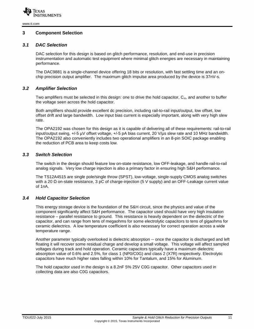
4.1 Pedestal Voltage vs Hold Capacitance
The charge injection of the switch, 3 pC, is used in Equation ( 6 ) to produce the Pedestal Error vs Capacitance graph, which is shown in Figure 12:
Figure 12. Pedestal Error
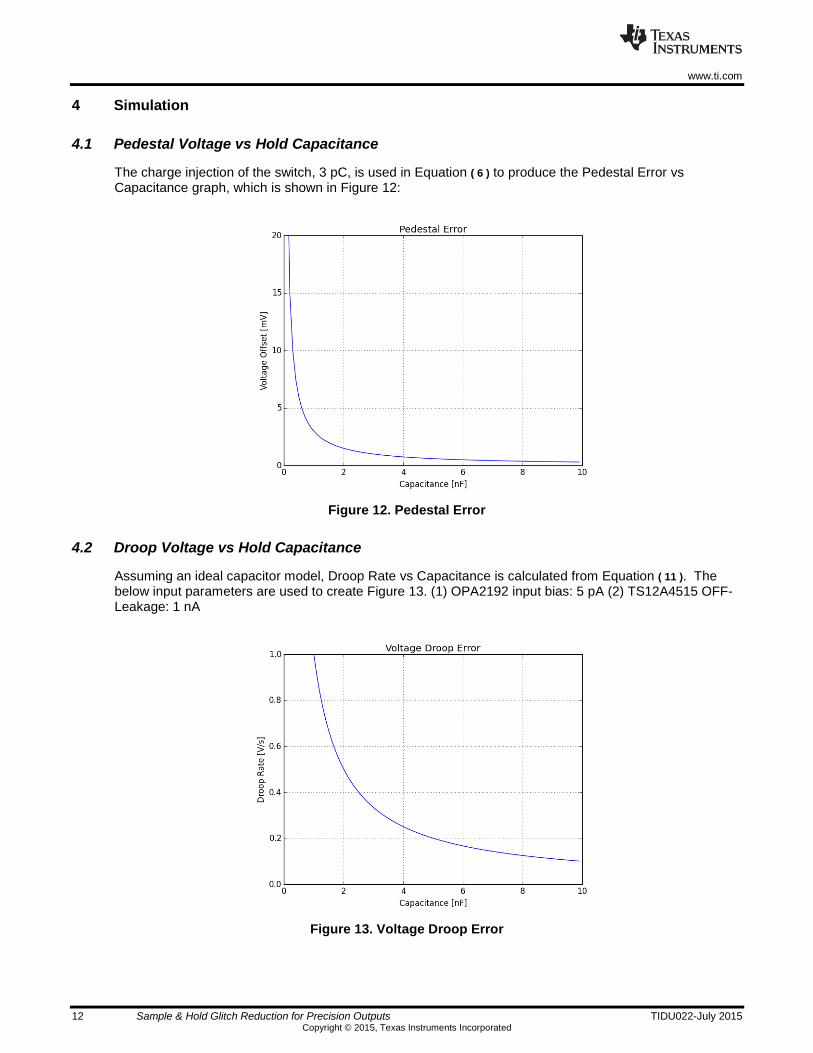
4.2 Droop Voltage vs Hold Capacitance
Assuming an ideal capacitor model, Droop Rate vs Capacitance is calculated from Equation ( 11 ). The below input parameters are used to create Figure 13. (1) OPA2192 input bias: 5 pA (2) TS12A4515 OFF-Leakage: 1 nA
Figure 13. Voltage Droop Error
www.ti.com
TIDU022-July 2015 Sample & Hold Glitch Reduction for Precision Outputs 13 Copyright © 2015, Texas Instruments Incorporated
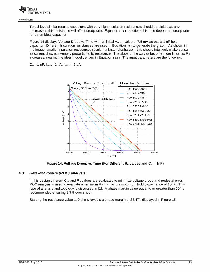
To achieve similar results, capacitors with very high insulation resistances should be picked as any decrease in this resistance will affect droop rate. Equation ( 10 ) describes this time dependent droop rate for a non-ideal capacitor.
Figure 14 displays Voltage Droop vs Time with an initial VHOLD value of 7.5 mV across a 1 nF hold capacitor. Different Insulation resistances are used in Equation ( 9 ) to generate the graph. As shown in the image, smaller insulation resistances result in a faster discharge -- this should intuitively make sense as current draw is inversely proportional to resistance. The slope of the curves become more linear as RP increases, nearing the ideal model derived in Equation ( 11 ). The input parameters are the following:
CH = 1 nF, ILEAK=1 nA, IBIAS = 5 pA.
VHOLD (initial voltage)
dV/dt = 1.005 [V/s]
Figure 14. Voltage Droop vs Time (For Different RP values and CH = 1nF)
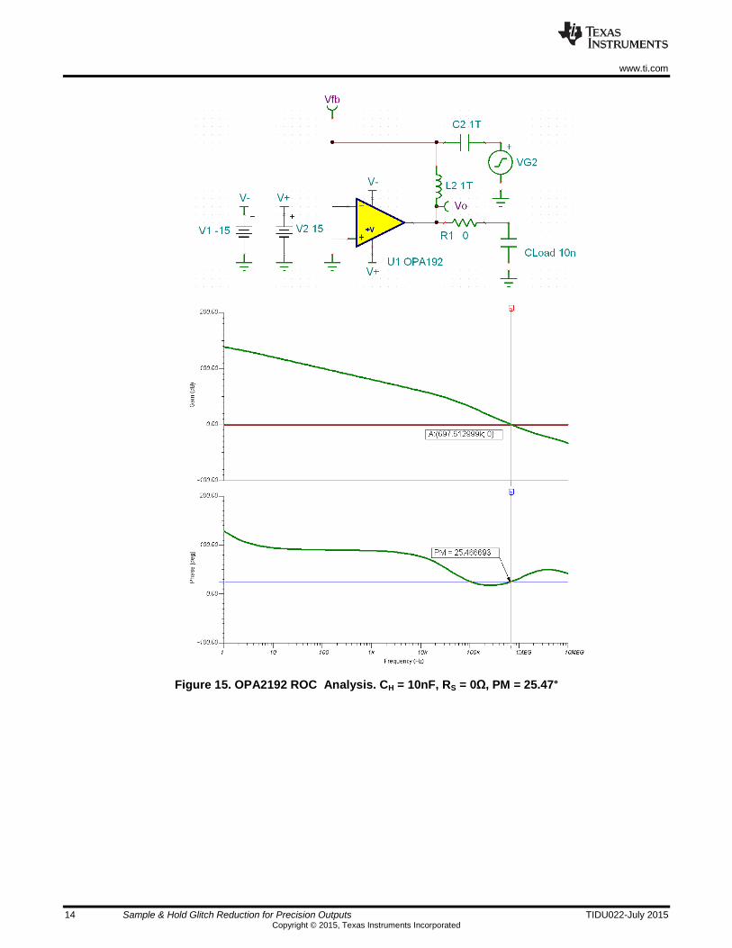
4.3 Rate-of-Closure (ROC) analysis
In this design different CH, and RS values are evaluated to minimize voltage droop and pedestal error. ROC analysis is used to evaluate a minimum RS in driving a maximum hold capacitance of 10nF. This
type of analysis and topology is discussed in [1]. A phase margin value equal to or greater than 60° is
recommended ensuring 8.7% over shoot.
Starting the resistance value at 0 ohms reveals a phase margin of 25.47°, displayed in Figure 15.
www.ti.com
14 Sample & Hold Glitch Reduction for Precision Outputs TIDU022-July 2015 Copyright © 2015, Texas Instruments Incorporated
Figure 15. OPA2192 ROC Analysis. CH = 10nF, RS = 0Ω, PM = 25.47°
www.ti.com
TIDU022-July 2015 Sample & Hold Glitch Reduction for Precision Outputs 15 Copyright © 2015, Texas Instruments Incorporated
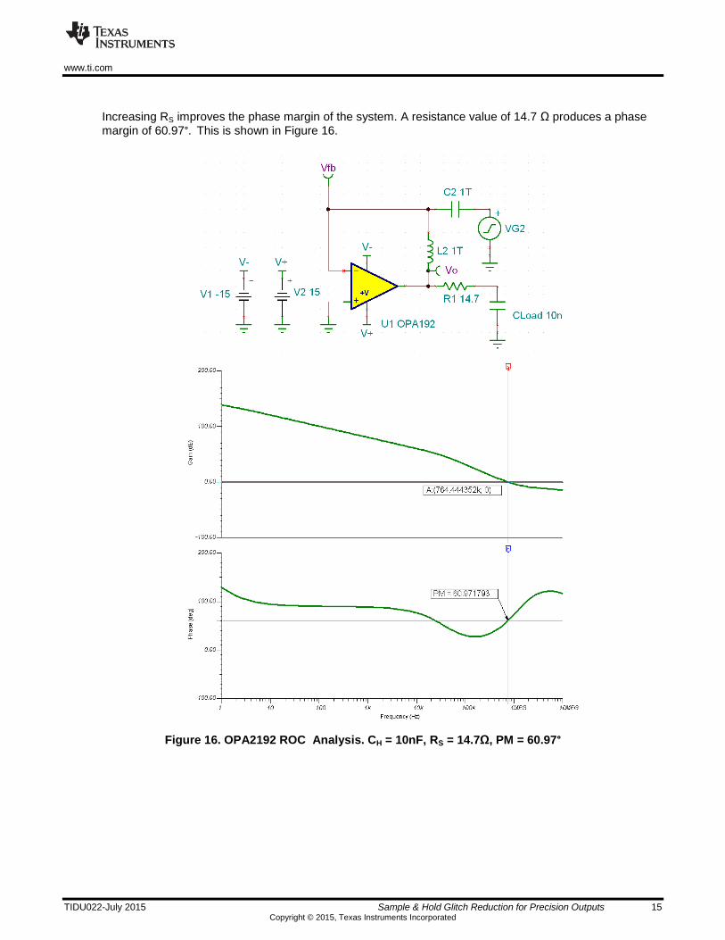
Increasing RS improves the phase margin of the system. A resistance value of 14.7 Ω produces a phase
margin of 60.97°. This is shown in Figure 16.
Figure 16. OPA2192 ROC Analysis. CH = 10nF, RS = 14.7Ω, PM = 60.97°
www.ti.com
16 Sample & Hold Glitch Reduction for Precision Outputs TIDU022-July 2015 Copyright © 2015, Texas Instruments Incorporated
4.4 Settling Time
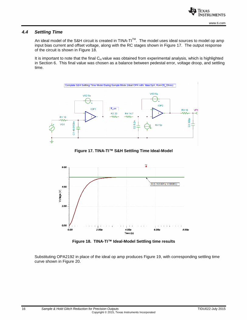
An ideal model of the S&H circuit is created in TINA-TITM
. The model uses ideal sources to model op amp input bias current and offset voltage, along with the RC stages shown in Figure 17. The output response of the circuit is shown in Figure 18.
It is important to note that the final CH value was obtained from experimental analysis, which is highlighted in Section 6. This final value was chosen as a balance between pedestal error, voltage droop, and settling time.
Figure 17. TINA-TI™ S&H Settling Time Ideal-Model
Figure 18. TINA-TI™ Ideal-Model Settling time results
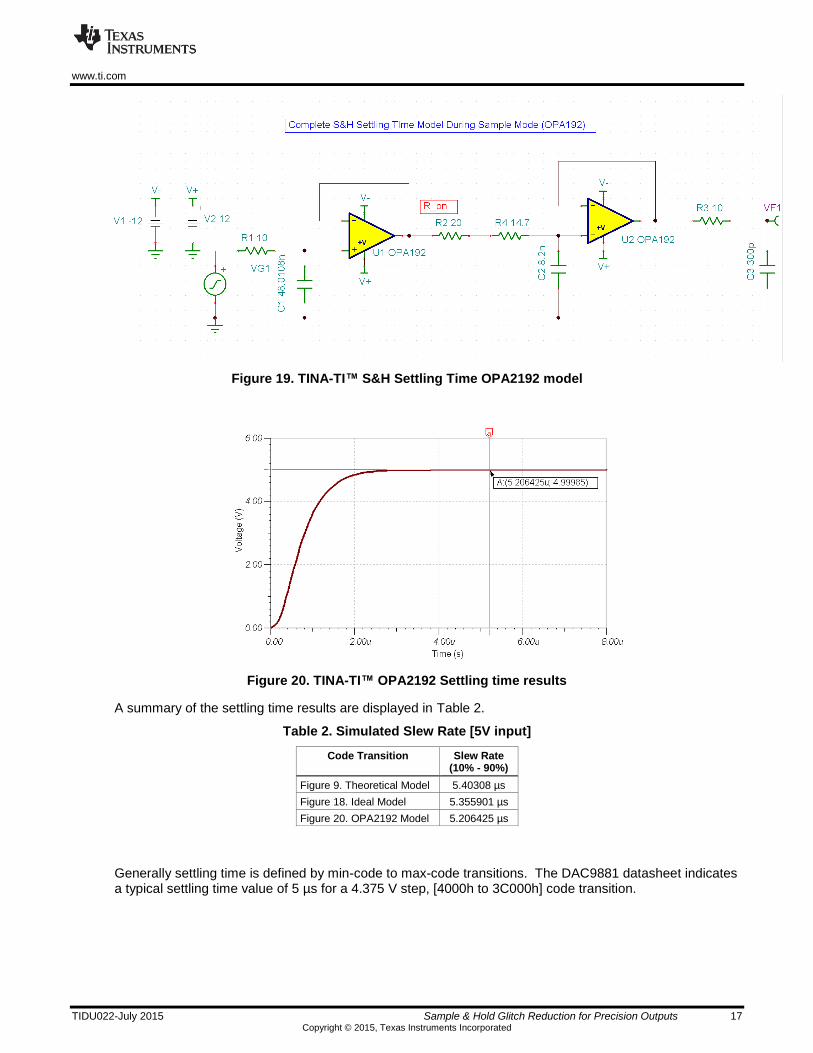
Substituting OPA2192 in place of the ideal op amp produces Figure 19, with corresponding settling time curve shown in Figure 20.
www.ti.com
TIDU022-July 2015 Sample & Hold Glitch Reduction for Precision Outputs 17 Copyright © 2015, Texas Instruments Incorporated
Figure 19. TINA-TI™ S&H Settling Time OPA2192 model
Figure 20. TINA-TI™ OPA2192 Settling time results
A summary of the settling time results are displayed in Table 2.
Table 2. Simulated Slew Rate [5V input]
Code Transition Slew Rate (10% - 90%)
Figure 9. Theoretical Model 5.40308 µs
Figure 18. Ideal Model 5.355901 µs
Figure 20. OPA2192 Model 5.206425 µs
Generally settling time is defined by min-code to max-code transitions. The DAC9881 datasheet indicates a typical settling time value of 5 µs for a 4.375 V step, [4000h to 3C000h] code transition.
www.ti.com
18 Sample & Hold Glitch Reduction for Precision Outputs TIDU022-July 2015 Copyright © 2015, Texas Instruments Incorporated
The previous equations and schematics accounted for a full-scale (0-5V) transition, but are modifiable in producing a new settling time estimate. This new estimate is shown in Table 3.
Table 3. Simulated Slew Rate [4.375V input]
Code Transition Slew Rate (10% - 90%)
Figure 9. Theoretical Model 5.33896 µs
Figure 18. Ideal Model 5.29347 µs
Figure 20. OPA2192 Model 5.140447 µs
4.5 TUE Error Calculation
Total unadjusted error (TUE) is obtained by computing the root square sum (RSS) of all errors generated from the DAC9881 and any passive or active components affecting gain, linearity, and offset.
Using information from the DAC9881 datasheet, integral non-linearity error is shown to have a maximum value of +/- 3 LSBs for the DAC9881S device. The INL error is converted to % FSR by using Equation ( 14
).
INLDAC(%FSR) = INLLSB
2bits∙ 100
( 13 )
INLDAC(%FSR) = 3LSB
218∙ 100 = 0.00114%
( 14 )
The gain error is also shown in the datasheet, having a maximum value of +/-32 LSBs. Equation ( 16 ) is used to convert gain error to %FSR.
GainErrorDAC(%FSR) = GainErrorLSB
2bits∙ 100
( 15 )
GainErrorDAC(%FSR) = 32LSB
218∙ 100 = 0.0122%
( 16 )
The DAC9881 includes an offset error which is created from the internal amplifier – the input bias currents of the internal amplifier interact with the R-2R output resulting in an offset voltage. The DAC9881 has a
maximum offset value of 16 LSBs for 25°C, and 32 LSBS over a temperature range of -40°C to +105°C.
Using a value of 16 LSBs and Equation ( 18 ), the offset error is converted to %FSR.
OffsetErrorDAC(%FSR) = OffsetErrorLSB
2bits∙ 100
( 17 )
OffsetErrorDAC(%FSR) = 16LSB
218∙ 100 = 0.0061%
( 18 )
The S&H circuit does not include any passive elements affecting gain, but two operational amplifier stages do add a small offset voltage to the overall characteristic transfer function, which does impact the TUE of the system. The OPA2192 specifies a typical offset voltage of +/-5 µV, and a maximum value of 75 µV
over a temperature range of -40°C to +105°C.
www.ti.com
TIDU022-July 2015 Sample & Hold Glitch Reduction for Precision Outputs 19 Copyright © 2015, Texas Instruments Incorporated
Using a value of 5 µV and Equation ( 20 ), the offset error generated from the op amp stages is converted in to %FSR.
OffsetErrorOPA(%FSR) = 2 ∙ VOPA_OFFSET
FullScaleRange∙ 100 ( 19 )
OffsetErrorOPA(%FSR) = 2 ∙ 5μV
5V∙ 100 = 0.0002%
( 20 )
All of the calculations performed above are included in the total unadjusted error, TUE, formula displayed in Equation ( 21 ). The equation combines all errors by taking the root square sum (RSS).
TUE =
√INLDAC2 + GainErrorDAC
2 + OffsetErrorDAC2+ OffsetErrorOPA
2 ( 21 )
TUE = 0.013689032% ( 22 )
www.ti.com
20 Sample & Hold Glitch Reduction for Precision Outputs TIDU022-July 2015 Copyright © 2015, Texas Instruments Incorporated
5 PCB Design
The PCB schematic and bill of materials can be found in Appendix A.
5.1 PCB Layout
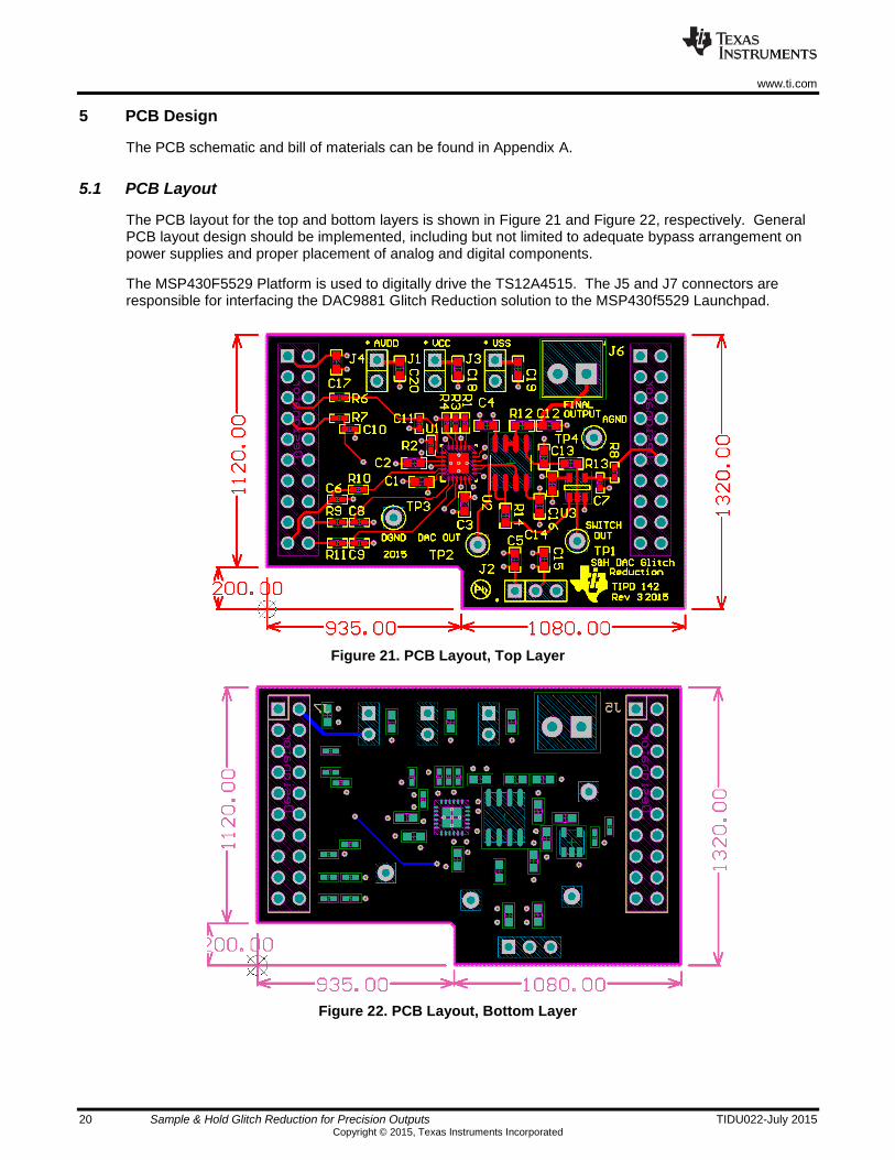
The PCB layout for the top and bottom layers is shown in Figure 21 and Figure 22, respectively. General PCB layout design should be implemented, including but not limited to adequate bypass arrangement on power supplies and proper placement of analog and digital components.
The MSP430F5529 Platform is used to digitally drive the TS12A4515. The J5 and J7 connectors are responsible for interfacing the DAC9881 Glitch Reduction solution to the MSP430f5529 Launchpad.
Figure 21. PCB Layout, Top Layer
Figure 22. PCB Layout, Bottom Layer
www.ti.com
TIDU022-July 2015 Sample & Hold Glitch Reduction for Precision Outputs 21 Copyright © 2015, Texas Instruments Incorporated
6 Verification & Measured Performance
6.1 Glitch Impulse Area (DAC Output vs S&H Output)
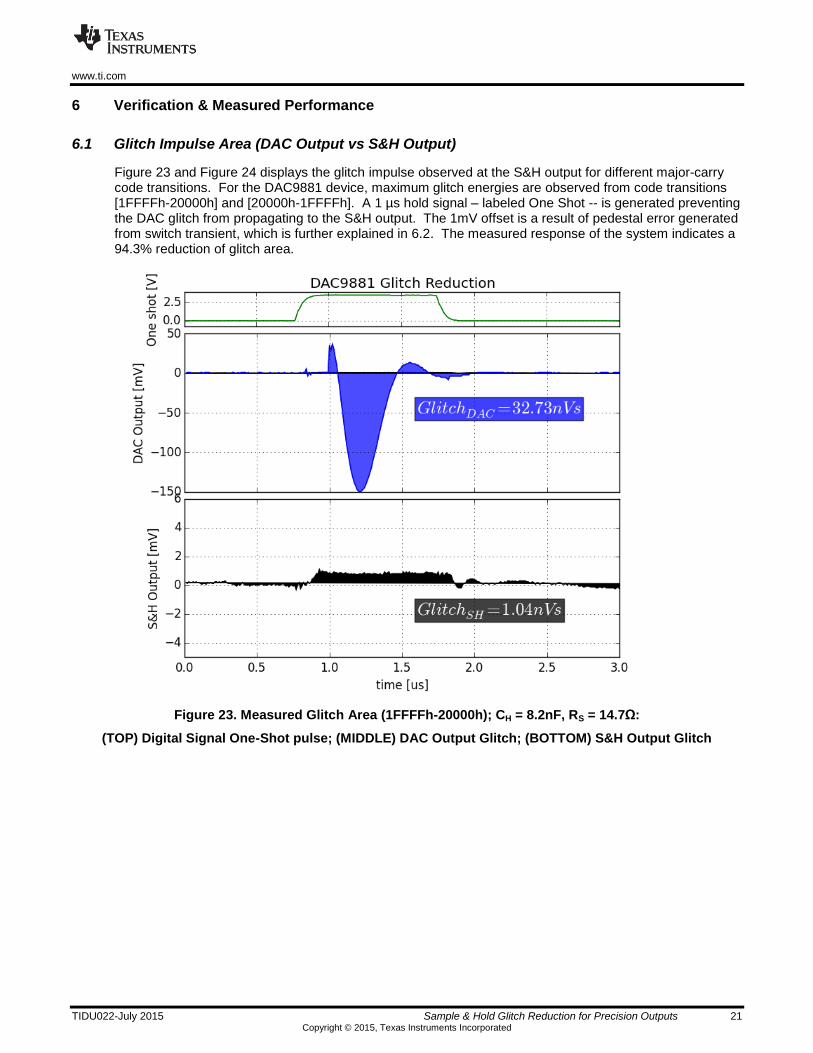
Figure 23 and Figure 24 displays the glitch impulse observed at the S&H output for different major-carry code transitions. For the DAC9881 device, maximum glitch energies are observed from code transitions [1FFFFh-20000h] and [20000h-1FFFFh]. A 1 µs hold signal – labeled One Shot -- is generated preventing the DAC glitch from propagating to the S&H output. The 1mV offset is a result of pedestal error generated from switch transient, which is further explained in 6.2. The measured response of the system indicates a 94.3% reduction of glitch area.
Figure 23. Measured Glitch Area (1FFFFh-20000h); CH = 8.2nF, RS = 14.7Ω:
(TOP) Digital Signal One-Shot pulse; (MIDDLE) DAC Output Glitch; (BOTTOM) S&H Output Glitch
www.ti.com
22 Sample & Hold Glitch Reduction for Precision Outputs TIDU022-July 2015 Copyright © 2015, Texas Instruments Incorporated
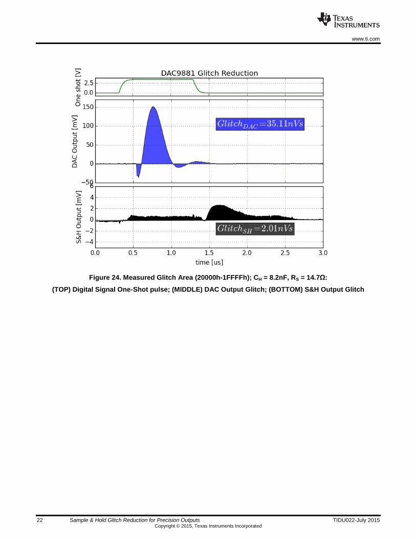
Figure 24. Measured Glitch Area (20000h-1FFFFh); CH = 8.2nF, RS = 14.7Ω:
(TOP) Digital Signal One-Shot pulse; (MIDDLE) DAC Output Glitch; (BOTTOM) S&H Output Glitch
www.ti.com
TIDU022-July 2015 Sample & Hold Glitch Reduction for Precision Outputs 23 Copyright © 2015, Texas Instruments Incorporated
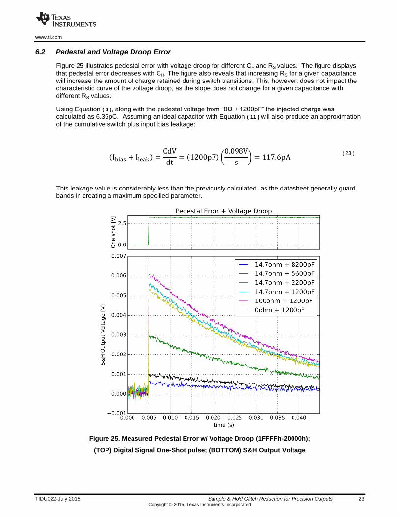
6.2 Pedestal and Voltage Droop Error
Figure 25 illustrates pedestal error with voltage droop for different CH and RS values. The figure displays that pedestal error decreases with CH. The figure also reveals that increasing RS for a given capacitance will increase the amount of charge retained during switch transitions. This, however, does not impact the characteristic curve of the voltage droop, as the slope does not change for a given capacitance with different RS values.
Using Equation ( 6 ), along with the pedestal voltage from “0Ω + 1200pF” the injected charge was calculated as 6.36pC. Assuming an ideal capacitor with Equation ( 11 ) will also produce an approximation of the cumulative switch plus input bias leakage:
(Ibias + Ileak) =CdV
dt= (1200pF) (
0.098V
s) = 117.6pA
( 23 )
This leakage value is considerably less than the previously calculated, as the datasheet generally guard bands in creating a maximum specified parameter.
Figure 25. Measured Pedestal Error w/ Voltage Droop (1FFFFh-20000h);
(TOP) Digital Signal One-Shot pulse; (BOTTOM) S&H Output Voltage
www.ti.com
24 Sample & Hold Glitch Reduction for Precision Outputs TIDU022-July 2015 Copyright © 2015, Texas Instruments Incorporated
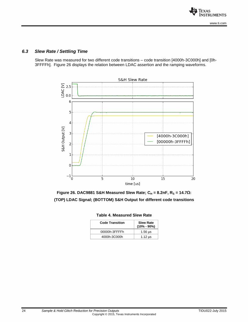
6.3 Slew Rate / Settling Time
Slew Rate was measured for two different code transitions – code transition [4000h-3C000h] and [0h-3FFFFh]. Figure 26 displays the relation between LDAC assertion and the ramping waveforms.
Figure 26. DAC9881 S&H Measured Slew Rate; CH = 8.2nF, RS = 14.7Ω:
(TOP) LDAC Signal; (BOTTOM) S&H Output for different code transitions
Table 4. Measured Slew Rate
Code Transition Slew Rate (10% - 90%)
00000h-3FFFFh 1.56 µs
4000h-3C000h 1.12 µs
www.ti.com
TIDU022-July 2015 Sample & Hold Glitch Reduction for Precision Outputs 25 Copyright © 2015, Texas Instruments Incorporated
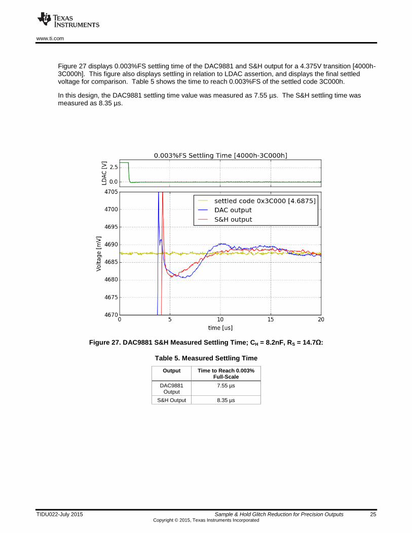
Figure 27 displays 0.003%FS settling time of the DAC9881 and S&H output for a 4.375V transition [4000h-3C000h]. This figure also displays settling in relation to LDAC assertion, and displays the final settled voltage for comparison. Table 5 shows the time to reach 0.003%FS of the settled code 3C000h.
In this design, the DAC9881 settling time value was measured as 7.55 µs. The S&H settling time was measured as 8.35 µs.
Figure 27. DAC9881 S&H Measured Settling Time; CH = 8.2nF, RS = 14.7Ω:
Table 5. Measured Settling Time
Output Time to Reach 0.003% Full-Scale
DAC9881 Output
7.55 µs
S&H Output 8.35 µs
www.ti.com
26 Sample & Hold Glitch Reduction for Precision Outputs TIDU022-July 2015 Copyright © 2015, Texas Instruments Incorporated
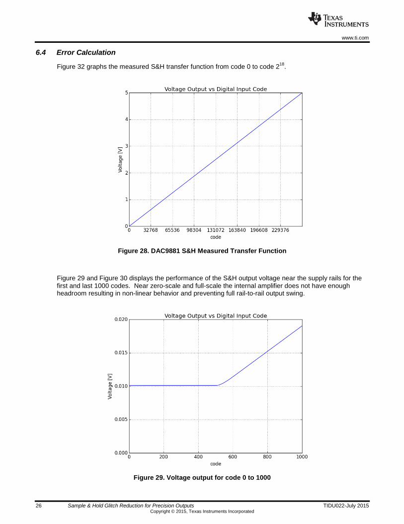
6.4 Error Calculation
Figure 32 graphs the measured S&H transfer function from code 0 to code 218
.
Figure 28. DAC9881 S&H Measured Transfer Function
Figure 29 and Figure 30 displays the performance of the S&H output voltage near the supply rails for the first and last 1000 codes. Near zero-scale and full-scale the internal amplifier does not have enough headroom resulting in non-linear behavior and preventing full rail-to-rail output swing.
Figure 29. Voltage output for code 0 to 1000
www.ti.com
TIDU022-July 2015 Sample & Hold Glitch Reduction for Precision Outputs 27 Copyright © 2015, Texas Instruments Incorporated
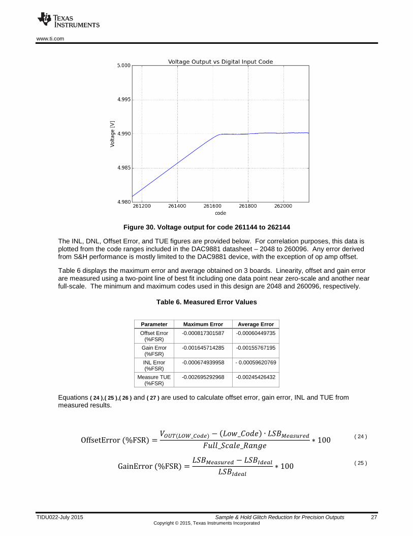
Figure 30. Voltage output for code 261144 to 262144
The INL, DNL, Offset Error, and TUE figures are provided below. For correlation purposes, this data is plotted from the code ranges included in the DAC9881 datasheet – 2048 to 260096. Any error derived from S&H performance is mostly limited to the DAC9881 device, with the exception of op amp offset.
Table 6 displays the maximum error and average obtained on 3 boards. Linearity, offset and gain error are measured using a two-point line of best fit including one data point near zero-scale and another near full-scale. The minimum and maximum codes used in this design are 2048 and 260096, respectively.
Table 6. Measured Error Values
Parameter Maximum Error Average Error
Offset Error (%FSR)
-0.000817301587 -0.00060449735
Gain Error (%FSR)
-0.001645714285 -0.00155767195
INL Error (%FSR)
-0.000674939958 - 0.00059620769
Measure TUE (%FSR)
-0.002695292968 -0.00245426432
Equations ( 24 ),( 25 ),( 26 ) and ( 27 ) are used to calculate offset error, gain error, INL and TUE from measured results.
OffsetError (%FSR) =𝑉𝑂𝑈𝑇(𝐿𝑂𝑊_𝐶𝑜𝑑𝑒) − (𝐿𝑜𝑤_𝐶𝑜𝑑𝑒) ∙ 𝐿𝑆𝐵𝑀𝑒𝑎𝑠𝑢𝑟𝑒𝑑
𝐹𝑢𝑙𝑙_𝑆𝑐𝑎𝑙𝑒_𝑅𝑎𝑛𝑔𝑒∗ 100
( 24 )
GainError (%FSR) =𝐿𝑆𝐵𝑀𝑒𝑎𝑠𝑢𝑟𝑒𝑑 − 𝐿𝑆𝐵𝐼𝑑𝑒𝑎𝑙
𝐿𝑆𝐵𝐼𝑑𝑒𝑎𝑙∗ 100
( 25 )
www.ti.com
28 Sample & Hold Glitch Reduction for Precision Outputs TIDU022-July 2015 Copyright © 2015, Texas Instruments Incorporated
𝐼𝑁𝐿(𝑘) = ∑(𝐷𝑁𝐿(𝑗))
𝑘
𝑗=0
( 26 )
TUE (%FSR) =𝑉𝐶𝑜𝑑𝑒(𝑀𝑒𝑎𝑠𝑢𝑟𝑒𝑑) − 𝑉𝐶𝑜𝑑𝑒(𝐼𝑑𝑒𝑎𝑙)
𝐹𝑢𝑙𝑙_𝑆𝑐𝑎𝑙𝑒_𝑅𝑎𝑛𝑔𝑒∗ 100
( 27 )
Where,
𝐿𝑆𝐵𝑀𝑒𝑎𝑠𝑢𝑟𝑒𝑑 = (𝑉_𝑂𝑈𝑇(𝐻𝑖𝑔ℎ_𝐶𝑜𝑑𝑒) − 𝑉_𝑂𝑈𝑇(𝐿𝑜𝑤_𝐶𝑜𝑑𝑒))
𝐻𝑖𝑔ℎ_𝐶𝑜𝑑𝑒−𝐿𝑜𝑤_𝐶𝑜𝑑𝑒
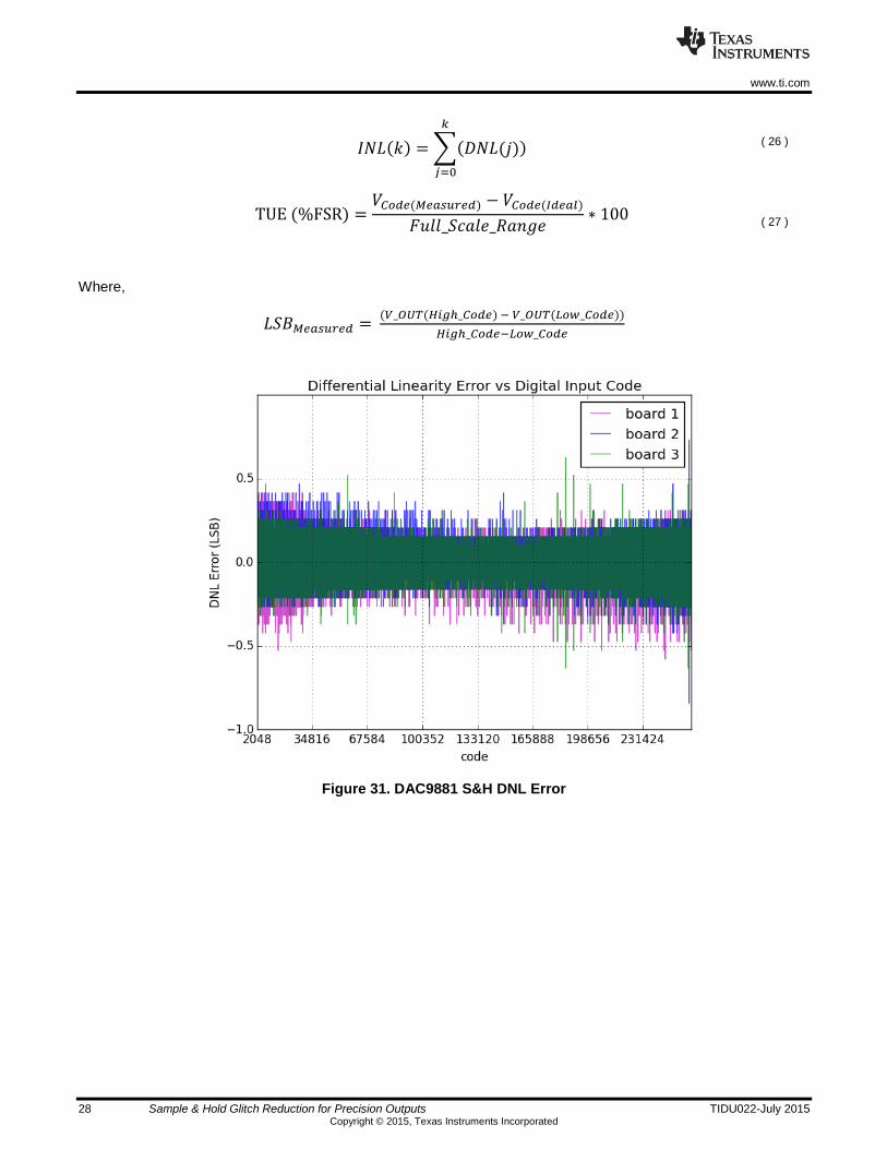
Figure 31. DAC9881 S&H DNL Error
www.ti.com
TIDU022-July 2015 Sample & Hold Glitch Reduction for Precision Outputs 29 Copyright © 2015, Texas Instruments Incorporated
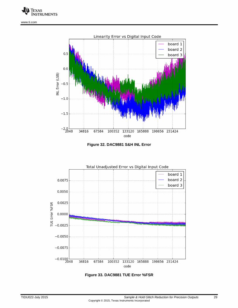
Figure 32. DAC9881 S&H INL Error
Figure 33. DAC9881 TUE Error %FSR
www.ti.com
30 Sample & Hold Glitch Reduction for Precision Outputs TIDU022-July 2015 Copyright © 2015, Texas Instruments Incorporated
7 Modifications
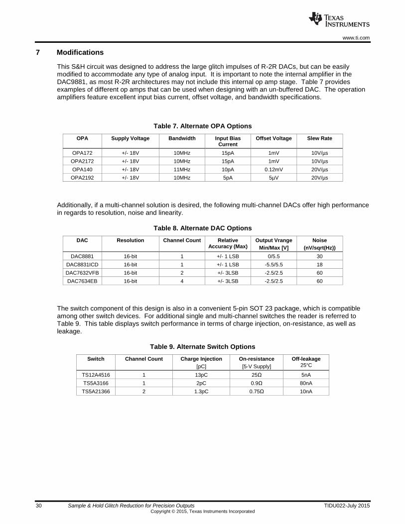
This S&H circuit was designed to address the large glitch impulses of R-2R DACs, but can be easily modified to accommodate any type of analog input. It is important to note the internal amplifier in the DAC9881, as most R-2R architectures may not include this internal op amp stage. Table 7 provides examples of different op amps that can be used when designing with an un-buffered DAC. The operation amplifiers feature excellent input bias current, offset voltage, and bandwidth specifications.
Table 7. Alternate OPA Options
OPA Supply Voltage Bandwidth Input Bias Current
Offset Voltage Slew Rate
OPA172 +/- 18V 10MHz 15pA 1mV 10V/µs
OPA2172 +/- 18V 10MHz 15pA 1mV 10V/µs
OPA140 +/- 18V 11MHz 10pA 0.12mV 20V/µs
OPA2192 +/- 18V 10MHz 5pA 5µV 20V/µs
Additionally, if a multi-channel solution is desired, the following multi-channel DACs offer high performance in regards to resolution, noise and linearity.
Table 8. Alternate DAC Options
DAC Resolution Channel Count Relative Accuracy (Max)
Output Vrange
Min/Max [V]
Noise
(nV/sqrt(Hz))
DAC8881 16-bit 1 +/- 1 LSB 0/5.5 30
DAC8831ICD 16-bit 1 +/- 1 LSB -5.5/5.5 18
DAC7632VFB 16-bit 2 +/- 3LSB -2.5/2.5 60
DAC7634EB 16-bit 4 +/- 3LSB -2.5/2.5 60
The switch component of this design is also in a convenient 5-pin SOT 23 package, which is compatible among other switch devices. For additional single and multi-channel switches the reader is referred to Table 9. This table displays switch performance in terms of charge injection, on-resistance, as well as leakage.
Table 9. Alternate Switch Options
Switch Channel Count Charge Injection
[pC]
On-resistance
[5-V Supply]
Off-leakage
25°C
TS12A4516 1 13pC 25Ω 5nA
TS5A3166 1 2pC 0.9Ω 80nA
TS5A21366 2 1.3pC 0.75Ω 10nA
www.ti.com
TIDU022-July 2015 Sample & Hold Glitch Reduction for Precision Outputs 31 Copyright © 2015, Texas Instruments Incorporated
8 About the Author
Matthew Sauceda is an applications engineer in the precision digital to analog converters group at Texas Instruments where he supports telecommunication and catalog products. Matthew received his MSEE from Texas A&M University in 2009.
www.ti.com
32 Sample & Hold Glitch Reduction for Precision Outputs TIDU022-July 2015 Copyright © 2015, Texas Instruments Incorporated
9 Acknowledgements & References
Online Sources:
1. P. Semig and Timothy Claycomb (2014), Capacitive Load Drive Solution using an Isolation Resistor , http://www.ti.com/lit/ug/tidu032c/tidu032c.pdf.
www.ti.com
TIDU022-July 2015 Sample & Hold Glitch Reduction for Precision Outputs 33 Copyright © 2015, Texas Instruments Incorporated
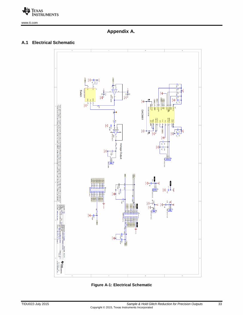
Appendix A.
A.1 Electrical Schematic
Figure A-1: Electrical Schematic
www.ti.com
34 Sample & Hold Glitch Reduction for Precision Outputs TIDU022-July 2015 Copyright © 2015, Texas Instruments Incorporated
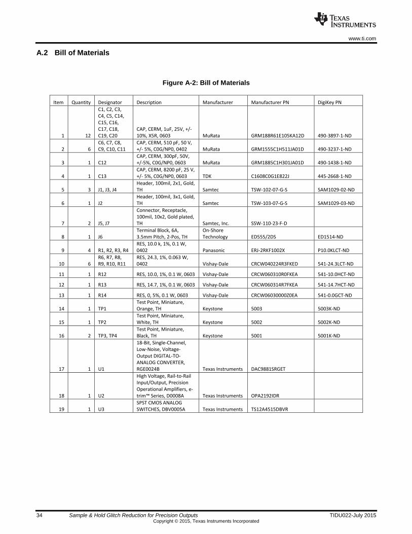
A.2 Bill of Materials
Figure A-2: Bill of Materials
Item Quantity Designator Description Manufacturer Manufacturer PN DigiKey PN
1 12
C1, C2, C3, C4, C5, C14, C15, C16, C17, C18, C19, C20
CAP, CERM, 1uF, 25V, +/-10%, X5R, 0603 MuRata GRM188R61E105KA12D 490-3897-1-ND
2 6 C6, C7, C8, C9, C10, C11
CAP, CERM, 510 pF, 50 V, +/- 5%, C0G/NP0, 0402 MuRata GRM1555C1H511JA01D 490-3237-1-ND
3 1 C12 CAP, CERM, 300pF, 50V, +/-5%, C0G/NP0, 0603 MuRata GRM1885C1H301JA01D 490-1438-1-ND
4 1 C13 CAP, CERM, 8200 pF, 25 V, +/- 5%, C0G/NP0, 0603 TDK C1608C0G1E822J 445-2668-1-ND
5 3 J1, J3, J4 Header, 100mil, 2x1, Gold, TH Samtec TSW-102-07-G-S SAM1029-02-ND
6 1 J2 Header, 100mil, 3x1, Gold, TH Samtec TSW-103-07-G-S SAM1029-03-ND
7 2 J5, J7
Connector, Receptacle, 100mil, 10x2, Gold plated, TH Samtec, Inc. SSW-110-23-F-D
8 1 J6 Terminal Block, 6A, 3.5mm Pitch, 2-Pos, TH
On-Shore Technology ED555/2DS ED1514-ND
9 4 R1, R2, R3, R4 RES, 10.0 k, 1%, 0.1 W, 0402 Panasonic ERJ-2RKF1002X P10.0KLCT-ND
10 6 R6, R7, R8, R9, R10, R11
RES, 24.3, 1%, 0.063 W, 0402 Vishay-Dale CRCW040224R3FKED 541-24.3LCT-ND
11 1 R12 RES, 10.0, 1%, 0.1 W, 0603 Vishay-Dale CRCW060310R0FKEA 541-10.0HCT-ND
12 1 R13 RES, 14.7, 1%, 0.1 W, 0603 Vishay-Dale CRCW060314R7FKEA 541-14.7HCT-ND
13 1 R14 RES, 0, 5%, 0.1 W, 0603 Vishay-Dale CRCW06030000Z0EA 541-0.0GCT-ND
14 1 TP1 Test Point, Miniature, Orange, TH Keystone 5003 5003K-ND
15 1 TP2 Test Point, Miniature, White, TH Keystone 5002 5002K-ND
16 2 TP3, TP4 Test Point, Miniature, Black, TH Keystone 5001 5001K-ND
17 1 U1
18-Bit, Single-Channel, Low-Noise, Voltage-Output DIGITAL-TO-ANALOG CONVERTER, RGE0024B Texas Instruments DAC9881SRGET
18 1 U2
High Voltage, Rail-to-Rail Input/Output, Precision Operational Amplifiers, e-trim™ Series, D0008A Texas Instruments OPA2192IDR
19 1 U3 SPST CMOS ANALOG SWITCHES, DBV0005A Texas Instruments TS12A4515DBVR
www.ti.com
TIDU022-July 2015 Sample & Hold Glitch Reduction for Precision Outputs 35 Copyright © 2015, Texas Instruments Incorporated
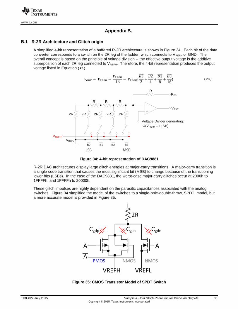
Appendix B.
B.1 R-2R Architecture and Glitch origin
A simplified 4-bit representation of a buffered R-2R architecture is shown in Figure 34. Each bit of the data converter corresponds to a switch on the 2R leg of the ladder, which connects to VREFH or GND. The overall concept is based on the principle of voltage division -- the effective output voltage is the additive superposition of each 2R leg connected to VREFH. Therefore, the 4-bit representation produces the output voltage listed in Equation ( 28 ).
𝑉𝑂𝑈𝑇 = 𝑉𝑅𝐸𝐹𝐻 − 𝑉𝑅𝐸𝐹𝐻
16− 𝑉𝑅𝐸𝐹𝐻(
𝐵3
2+
𝐵2
4+
𝐵1
8+
𝐵0
16)
( 28 )
2R2R2R2R
VREFH
2R
VOUT
RFB
+
R
½(VREFH – 1LSB)
MSB
R R
R
Voltage Divider generating:
LSB
B3B2B1B0
VREFL
Figure 34: 4-bit representation of DAC9881
R-2R DAC architectures display large glitch energies at major-carry transitions. A major-carry transition is a single-code transition that causes the most significant bit (MSB) to change because of the transitioning lower bits (LSBs). In the case of the DAC9881, the worst-case major-carry glitches occur at 2000h to 1FFFFh, and 1FFFFh to 20000h.
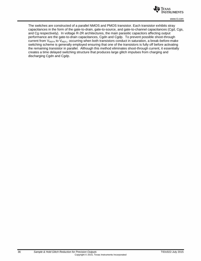
These glitch impulses are highly dependent on the parasitic capacitances associated with the analog switches. Figure 34 simplified the model of the switches to a single-pole-double-throw, SPDT, model, but a more accurate model is provided in Figure 35.
VREFH VREFL
A A
2R
APMOS NMOS NMOS
CgdnCgdp Cgsn
Figure 35: CMOS Transistor Model of SPDT Switch
www.ti.com
36 Sample & Hold Glitch Reduction for Precision Outputs TIDU022-July 2015 Copyright © 2015, Texas Instruments Incorporated
The switches are constructed of a parallel NMOS and PMOS transistor. Each transistor exhibits stray capacitances in the form of the gate-to-drain, gate-to-source, and gate-to-channel capacitances (Cgd, Cgs, and Cg respectively). In voltage R-2R architectures, the main parasitic capacitors affecting output performance are the gate-to-drain capacitances, Cgdn and Cgdp. To prevent possible shoot-through current from VREFH to VREFL, occurring when both transistors conduct in saturation, a break-before-make switching scheme is generally employed ensuring that one of the transistors is fully off before activating the remaining transistor in parallel. Although this method eliminates shoot-through current, it essentially creates a time delayed switching structure that produces large glitch impulses from charging and discharging Cgdn and Cgdp.
www.ti.com
TIDU022-July 2015 Sample & Hold Glitch Reduction for Precision Outputs 37 Copyright © 2015, Texas Instruments Incorporated
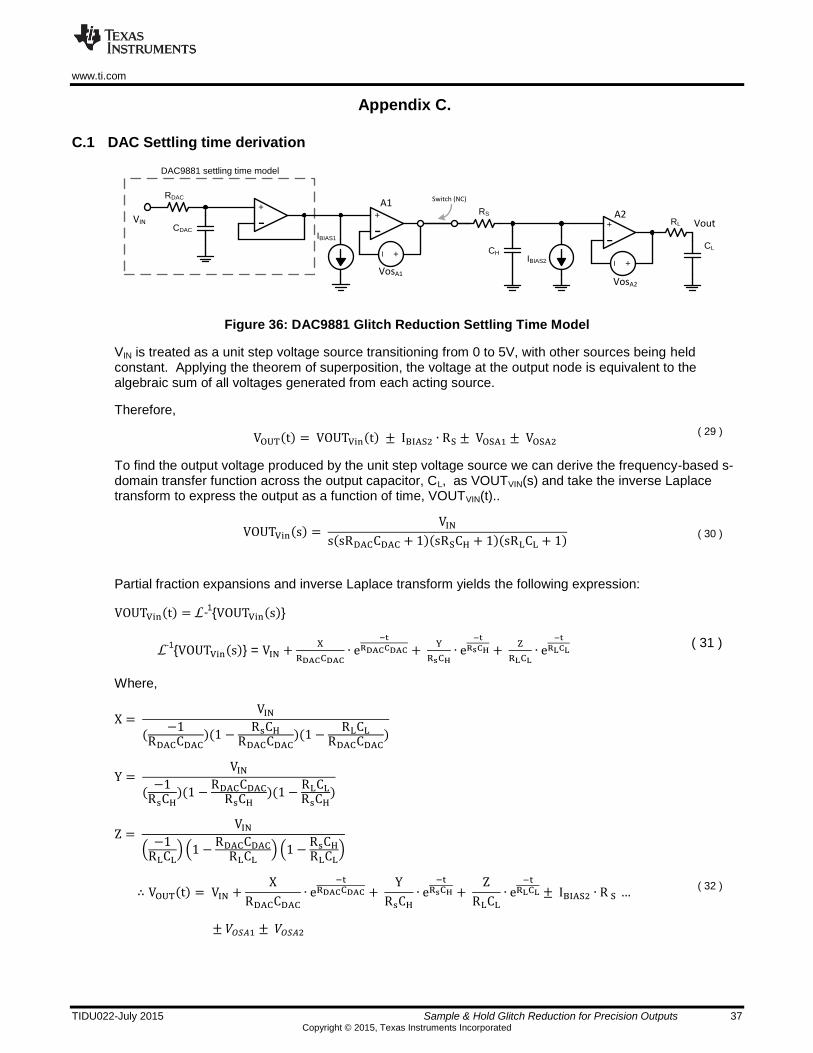
Appendix C.
C.1 DAC Settling time derivation
RDAC
+
CDAC
RS
CH
+ RL
CL
IBIAS2
Switch (NC)
+
IBIAS1
DAC9881 settling time model
VIN Vout
A1A2
+–
VosA1
VosA2
+–
Figure 36: DAC9881 Glitch Reduction Settling Time Model
VIN is treated as a unit step voltage source transitioning from 0 to 5V, with other sources being held constant. Applying the theorem of superposition, the voltage at the output node is equivalent to the algebraic sum of all voltages generated from each acting source.
Therefore,
VOUT(t) = VOUTVin(t) ± IBIAS2 ∙ RS ± VOSA1 ± VOSA2 ( 29 )
To find the output voltage produced by the unit step voltage source we can derive the frequency-based s-domain transfer function across the output capacitor, CL, as VOUTVIN(s) and take the inverse Laplace transform to express the output as a function of time, VOUTVIN(t)..
VOUTVin(s) = VIN
s(sRDACCDAC + 1)(sRSCH + 1)(sRLCL + 1)
( 30 )
Partial fraction expansions and inverse Laplace transform yields the following expression:
VOUTVin(t) = L-1VOUTVin(s)
L-1VOUTVin(s) = VIN +
X
RDACCDAC∙ e
−t
RDACCDAC + Y
RsCH∙ e
−t
RsCH + Z
RLCL∙ e
−t
RLCL ( 31 )
Where,
X = VIN
(−1
RDACCDAC)(1 −
RsCH
RDACCDAC)(1 −
RLCL
RDACCDAC)
Y = VIN
(−1
RsCH)(1 −
RDACCDAC
RsCH)(1 −
RLCL
RsCH)
Z = VIN
(−1
RLCL) (1 −
RDACCDAC
RLCL) (1 −
RsCH
RLCL)
∴ VOUT(t) = VIN +X
RDACCDAC
∙ e−t
RDACCDAC + Y
RsCH
∙ e−t
RsCH + Z
RLCL
∙ e−t
RLCL ± IBIAS2 ∙ R S … ( 32 )
± 𝑉𝑂𝑆𝐴1 ± 𝑉𝑂𝑆𝐴2
IMPORTANT NOTICE FOR TI REFERENCE DESIGNS
Texas Instruments Incorporated ("TI") reference designs are solely intended to assist designers (“Buyers”) who are developing systems thatincorporate TI semiconductor products (also referred to herein as “components”). Buyer understands and agrees that Buyer remainsresponsible for using its independent analysis, evaluation and judgment in designing Buyer’s systems and products.TI reference designs have been created using standard laboratory conditions and engineering practices. TI has not conducted anytesting other than that specifically described in the published documentation for a particular reference design. TI may makecorrections, enhancements, improvements and other changes to its reference designs.Buyers are authorized to use TI reference designs with the TI component(s) identified in each particular reference design and to modify thereference design in the development of their end products. HOWEVER, NO OTHER LICENSE, EXPRESS OR IMPLIED, BY ESTOPPELOR OTHERWISE TO ANY OTHER TI INTELLECTUAL PROPERTY RIGHT, AND NO LICENSE TO ANY THIRD PARTY TECHNOLOGYOR INTELLECTUAL PROPERTY RIGHT, IS GRANTED HEREIN, including but not limited to any patent right, copyright, mask work right,or other intellectual property right relating to any combination, machine, or process in which TI components or services are used.Information published by TI regarding third-party products or services does not constitute a license to use such products or services, or awarranty or endorsement thereof. Use of such information may require a license from a third party under the patents or other intellectualproperty of the third party, or a license from TI under the patents or other intellectual property of TI.TI REFERENCE DESIGNS ARE PROVIDED "AS IS". TI MAKES NO WARRANTIES OR REPRESENTATIONS WITH REGARD TO THEREFERENCE DESIGNS OR USE OF THE REFERENCE DESIGNS, EXPRESS, IMPLIED OR STATUTORY, INCLUDING ACCURACY ORCOMPLETENESS. TI DISCLAIMS ANY WARRANTY OF TITLE AND ANY IMPLIED WARRANTIES OF MERCHANTABILITY, FITNESSFOR A PARTICULAR PURPOSE, QUIET ENJOYMENT, QUIET POSSESSION, AND NON-INFRINGEMENT OF ANY THIRD PARTYINTELLECTUAL PROPERTY RIGHTS WITH REGARD TO TI REFERENCE DESIGNS OR USE THEREOF. TI SHALL NOT BE LIABLEFOR AND SHALL NOT DEFEND OR INDEMNIFY BUYERS AGAINST ANY THIRD PARTY INFRINGEMENT CLAIM THAT RELATES TOOR IS BASED ON A COMBINATION OF COMPONENTS PROVIDED IN A TI REFERENCE DESIGN. IN NO EVENT SHALL TI BELIABLE FOR ANY ACTUAL, SPECIAL, INCIDENTAL, CONSEQUENTIAL OR INDIRECT DAMAGES, HOWEVER CAUSED, ON ANYTHEORY OF LIABILITY AND WHETHER OR NOT TI HAS BEEN ADVISED OF THE POSSIBILITY OF SUCH DAMAGES, ARISING INANY WAY OUT OF TI REFERENCE DESIGNS OR BUYER’S USE OF TI REFERENCE DESIGNS.TI reserves the right to make corrections, enhancements, improvements and other changes to its semiconductor products and services perJESD46, latest issue, and to discontinue any product or service per JESD48, latest issue. Buyers should obtain the latest relevantinformation before placing orders and should verify that such information is current and complete. All semiconductor products are soldsubject to TI’s terms and conditions of sale supplied at the time of order acknowledgment.TI warrants performance of its components to the specifications applicable at the time of sale, in accordance with the warranty in TI’s termsand conditions of sale of semiconductor products. Testing and other quality control techniques for TI components are used to the extent TIdeems necessary to support this warranty. Except where mandated by applicable law, testing of all parameters of each component is notnecessarily performed.TI assumes no liability for applications assistance or the design of Buyers’ products. Buyers are responsible for their products andapplications using TI components. To minimize the risks associated with Buyers’ products and applications, Buyers should provideadequate design and operating safeguards.Reproduction of significant portions of TI information in TI data books, data sheets or reference designs is permissible only if reproduction iswithout alteration and is accompanied by all associated warranties, conditions, limitations, and notices. TI is not responsible or liable forsuch altered documentation. Information of third parties may be subject to additional restrictions.Buyer acknowledges and agrees that it is solely responsible for compliance with all legal, regulatory and safety-related requirementsconcerning its products, and any use of TI components in its applications, notwithstanding any applications-related information or supportthat may be provided by TI. Buyer represents and agrees that it has all the necessary expertise to create and implement safeguards thatanticipate dangerous failures, monitor failures and their consequences, lessen the likelihood of dangerous failures and take appropriateremedial actions. Buyer will fully indemnify TI and its representatives against any damages arising out of the use of any TI components inBuyer’s safety-critical applications.In some cases, TI components may be promoted specifically to facilitate safety-related applications. With such components, TI’s goal is tohelp enable customers to design and create their own end-product solutions that meet applicable functional safety standards andrequirements. Nonetheless, such components are subject to these terms.No TI components are authorized for use in FDA Class III (or similar life-critical medical equipment) unless authorized officers of the partieshave executed an agreement specifically governing such use.Only those TI components that TI has specifically designated as military grade or “enhanced plastic” are designed and intended for use inmilitary/aerospace applications or environments. Buyer acknowledges and agrees that any military or aerospace use of TI components thathave not been so designated is solely at Buyer's risk, and Buyer is solely responsible for compliance with all legal and regulatoryrequirements in connection with such use.TI has specifically designated certain components as meeting ISO/TS16949 requirements, mainly for automotive use. In any case of use ofnon-designated products, TI will not be responsible for any failure to meet ISO/TS16949.IMPORTANT NOTICE
Mailing Address: Texas Instruments, Post Office Box 655303, Dallas, Texas 75265Copyright © 2015, Texas Instruments Incorporated