Embed Size (px)
Citation preview
On the RF system of the ILC
Sami G. Tantawi
Chris NantistaValery Dolgashev
Jiquan Guo
SLAC

Outline• This talk is a collection of thoughts about the rf
system based on our experience with X-band system!
• Review of the X-band RF systems• The main linac division into separate system, A
bad idea• Examples from a system point:
– The distribution system and relations to structure spacing
– Rf source developments and relations to modulator and couplers
• Some thoughts on couplers
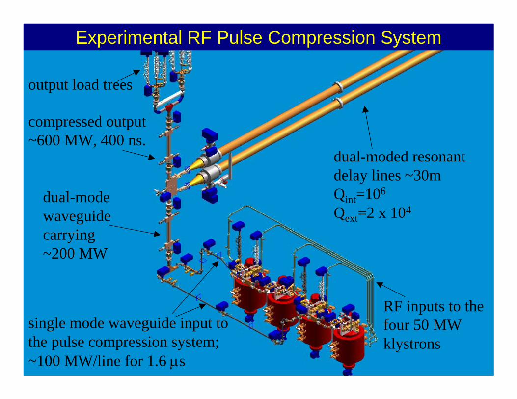
dual-moded resonant delay lines ~30mQint=106
Qext=2 x 10⁴
RF inputs to the four 50 MW klystrons
single mode waveguide input to the pulse compression system; ~100 MW/line for 1.6 µs
dual-mode waveguide carrying ~200 MW
compressed output ~600 MW, 400 ns.
output load trees
Experimental RF Pulse Compression System
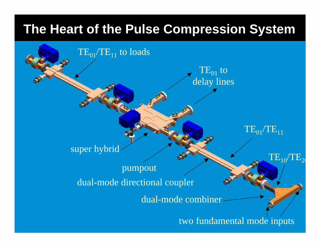
The Heart of the Pulse Compression System
dual-mode combiner
two fundamental mode inputs
TE10/TE20
TE01/TE11
dual-mode directional couplerpumpout
super hybrid
TE01 to delay lines
TE01/TE11 to loads
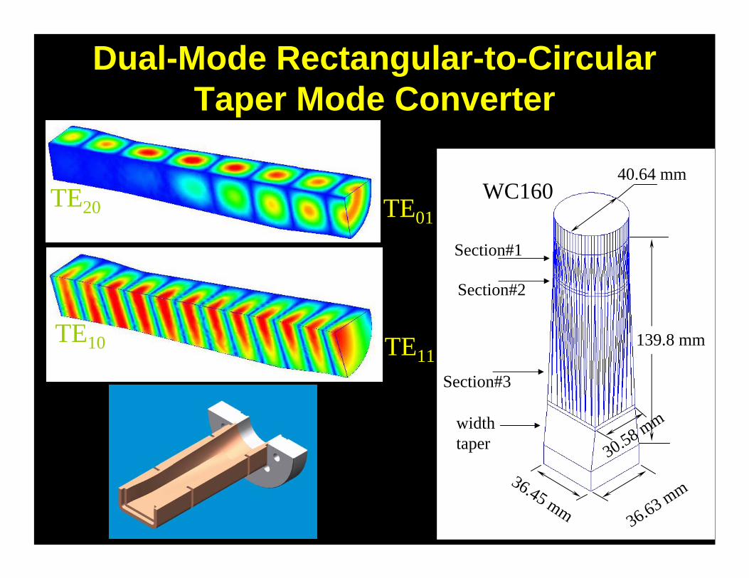
Dual-Mode Rectangular-to-Circular Taper Mode Converter
TE01
139.8 mm
40.64 mm
36.45 mm
30.58 mm
WC160
Section#1
Section#2
Section#3
width taper
36.63 mm
TE11
TE20
TE10
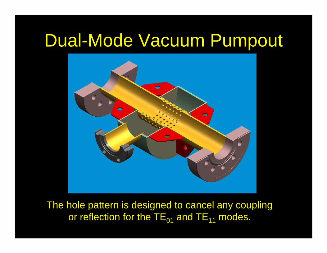
Dual-Mode Vacuum Pumpout
The hole pattern is designed to cancel any coupling or reflection for the TE01 and TE11 modes.
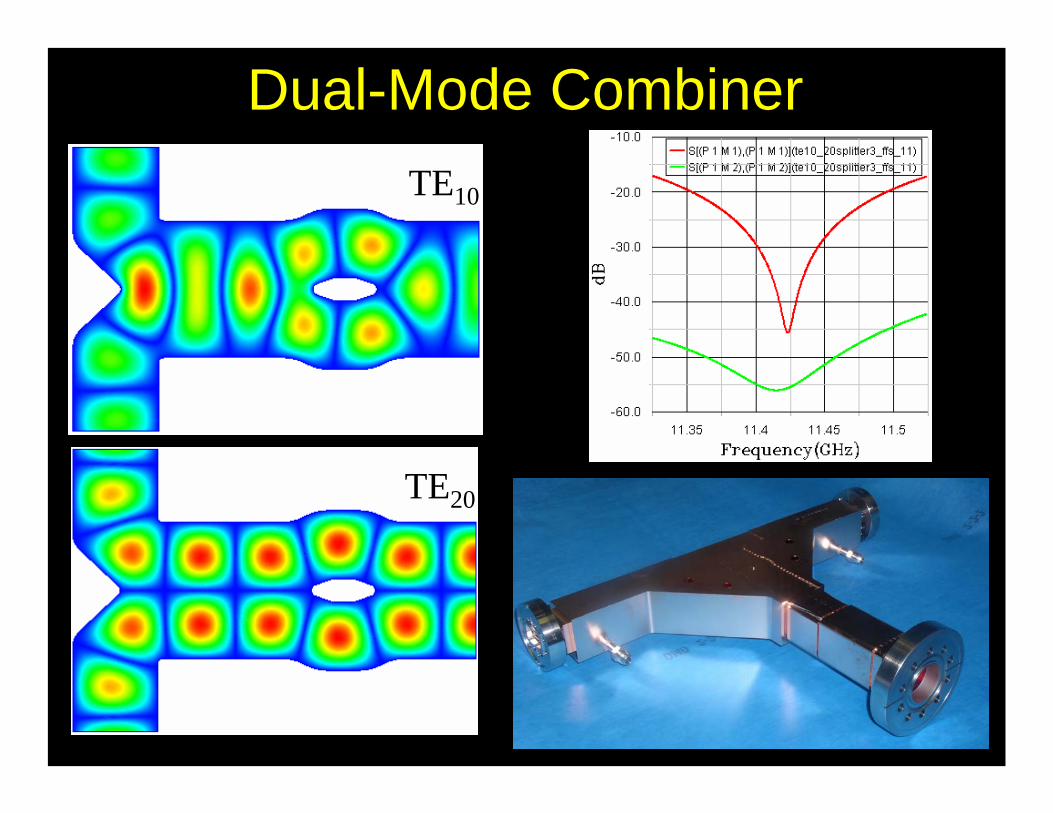
Dual-Mode CombinerTE10
TE20
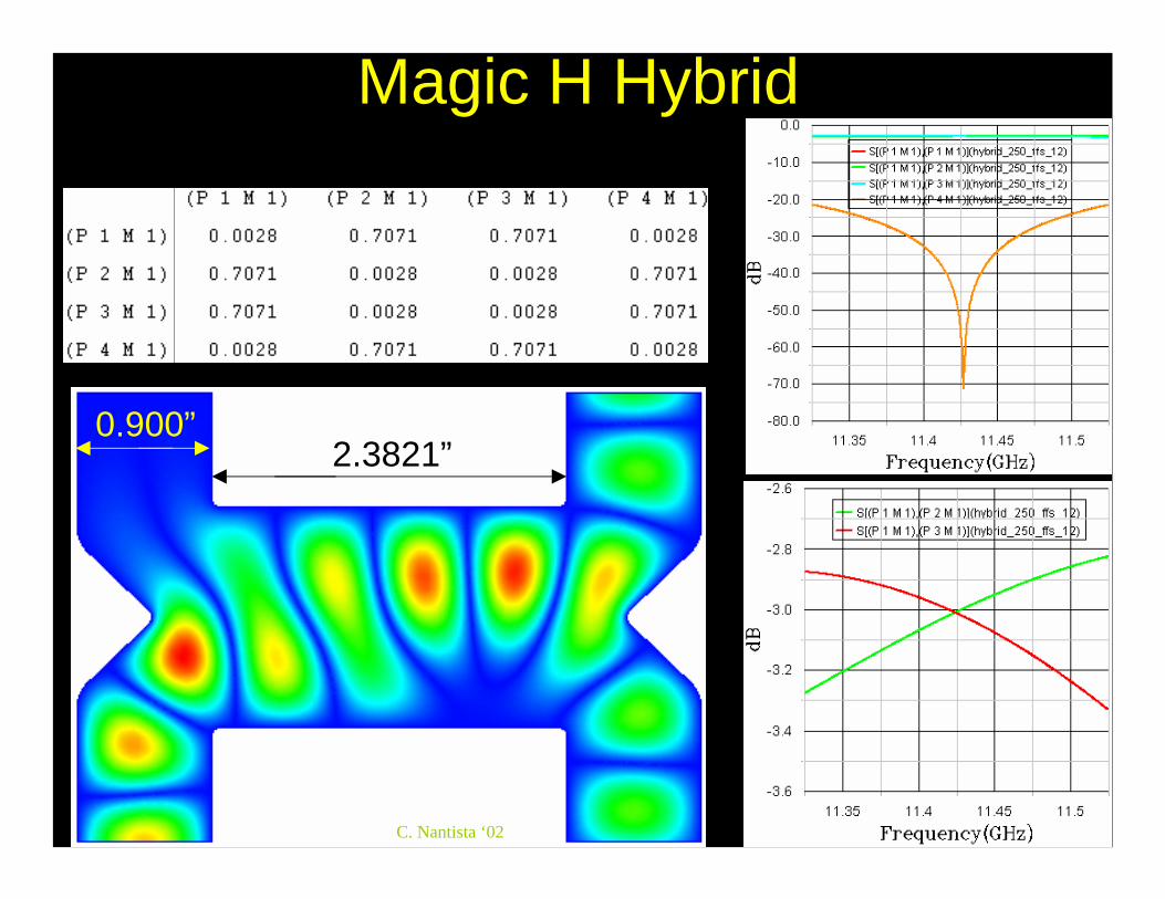
Magic H Hybrid
2.3821”0.900”
C. Nantista ‘02
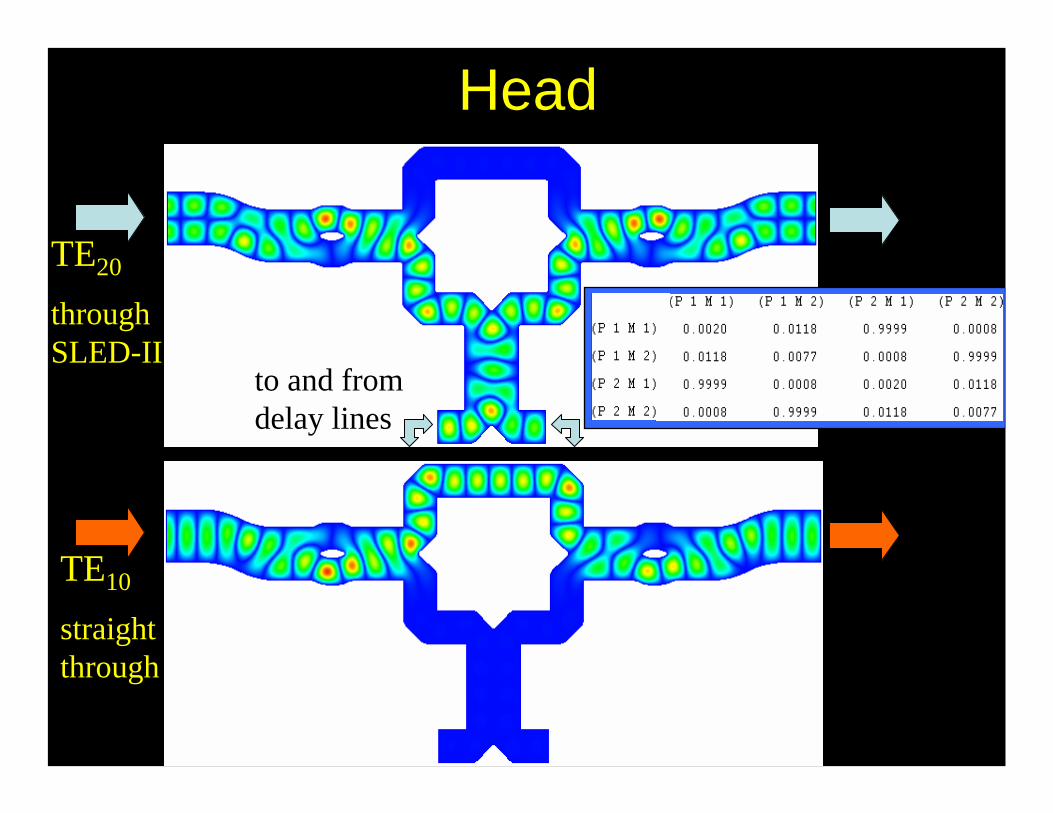
Head
TE10
straight through
TE20
through SLED-II
to and from delay lines
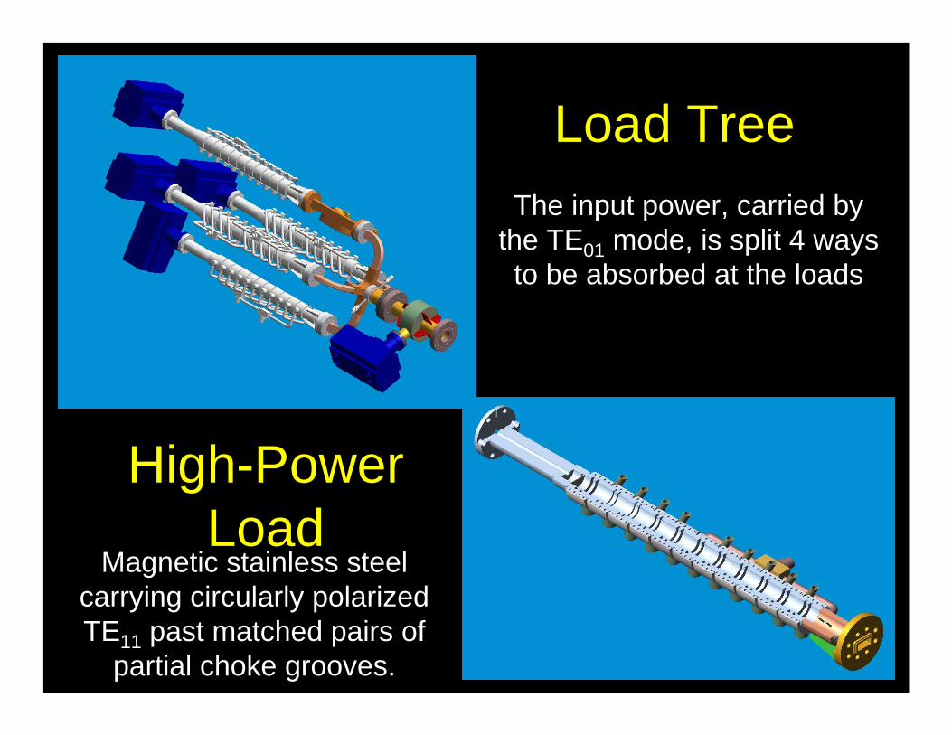
The input power, carried by the TE01 mode, is split 4 ways to be absorbed at the loads
Load Tree
High-Power Load
Magnetic stainless steel carrying circularly polarized TE11 past matched pairs of
partial choke grooves.
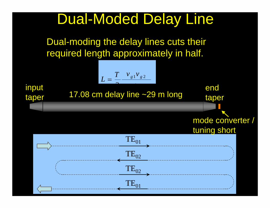
Dual-Moded Delay Line
TE01
TE02
TE02
TE01
17.08 cm delay line ~29 m longinput taper
end taper
mode converter / tuning short
Dual-moding the delay lines cuts their required length approximately in half.
21
21
2 gg
gg
vvvvTL+
=
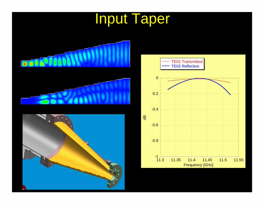
Input Taper
-1
-0.8
-0.6
-0.4
-0.2
0
11.3 11.35 11.4 11.45 11.5 11.55
TE01 Transmitted TE02 Reflection
dB
Frequency [GHz]

System Layout
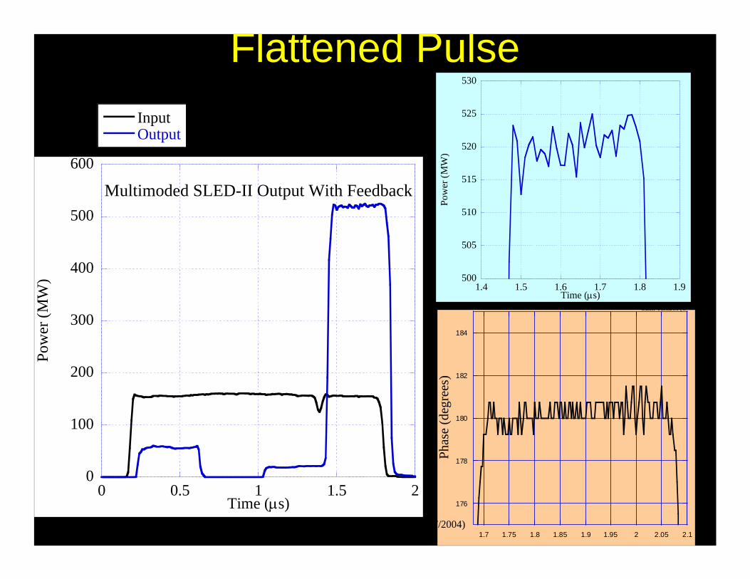
Flattened Pulse
0
100
200
300
400
500
600
0 0.5 1 1.5 2
InputOutput
Pow
er (M
W)
Time (µs)Sami Tantawi (1/27/2004)
176
178
180
182
184
1.7 1.75 1.8 1.85 1.9 1.95 2 2.05 2.1
500
505
510
515
520
525
530
1.4 1.5 1.6 1.7 1.8 1.9
Pow
er (M
W)
Time (µs)Sami Tantawi (1/2
Multimoded SLED-II Output With Feedback
Phas
e (d
egre
es)
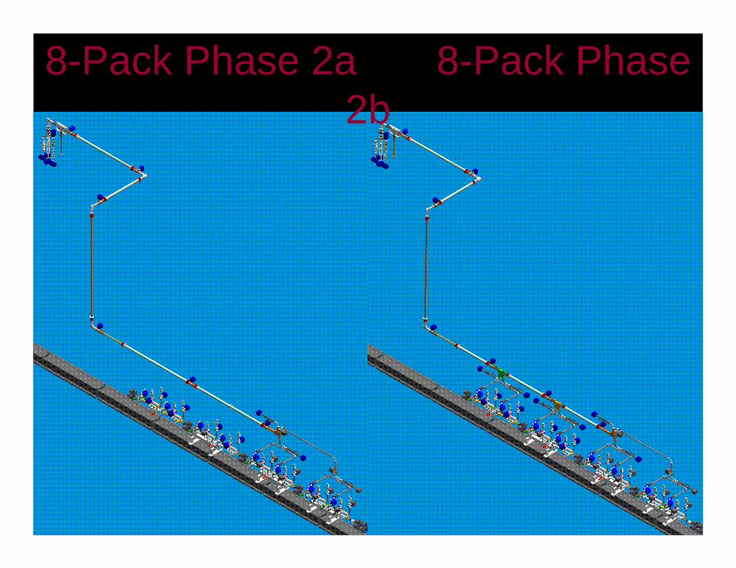
8-Pack Phase 2a 8-Pack Phase 2b
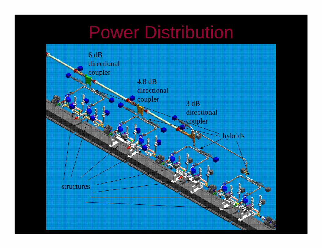
Power Distribution6 dB directional coupler
4.8 dB directional coupler 3 dB
directional coupler
hybrids
structures

Highlights from the X-Band System• We have reliably produced and manipulated flat
400 ns rf pulses carrying over 500 MW.• We have developed waveguide components
capable of manipulating hundreds of megawatts.• We have utilized dual-moding, both for power
direction and for shortening delay lines.• The circular TE01 mode is a miracle mode solves all
problems• The charging and discharging of the delay lines
could be improved with active elements• We could not relay on circulators, they do not exist
at these power levels.
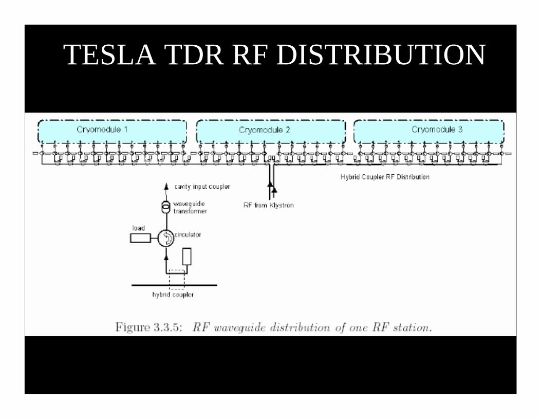
TESLA TDR RF DISTRIBUTION
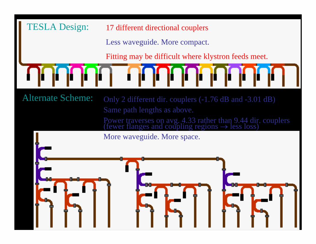
TESLA Design:
Alternate Scheme:
2:1
1:1
17 different directional couplers
Less waveguide. More compact.
Fitting may be difficult where klystron feeds meet.
Only 2 different dir. couplers (-1.76 dB and -3.01 dB)Same path lengths as above.Power traverses on avg. 4.33 rather than 9.44 dir. couplers (fewer flanges and coupling regions → less loss)More waveguide. More space.
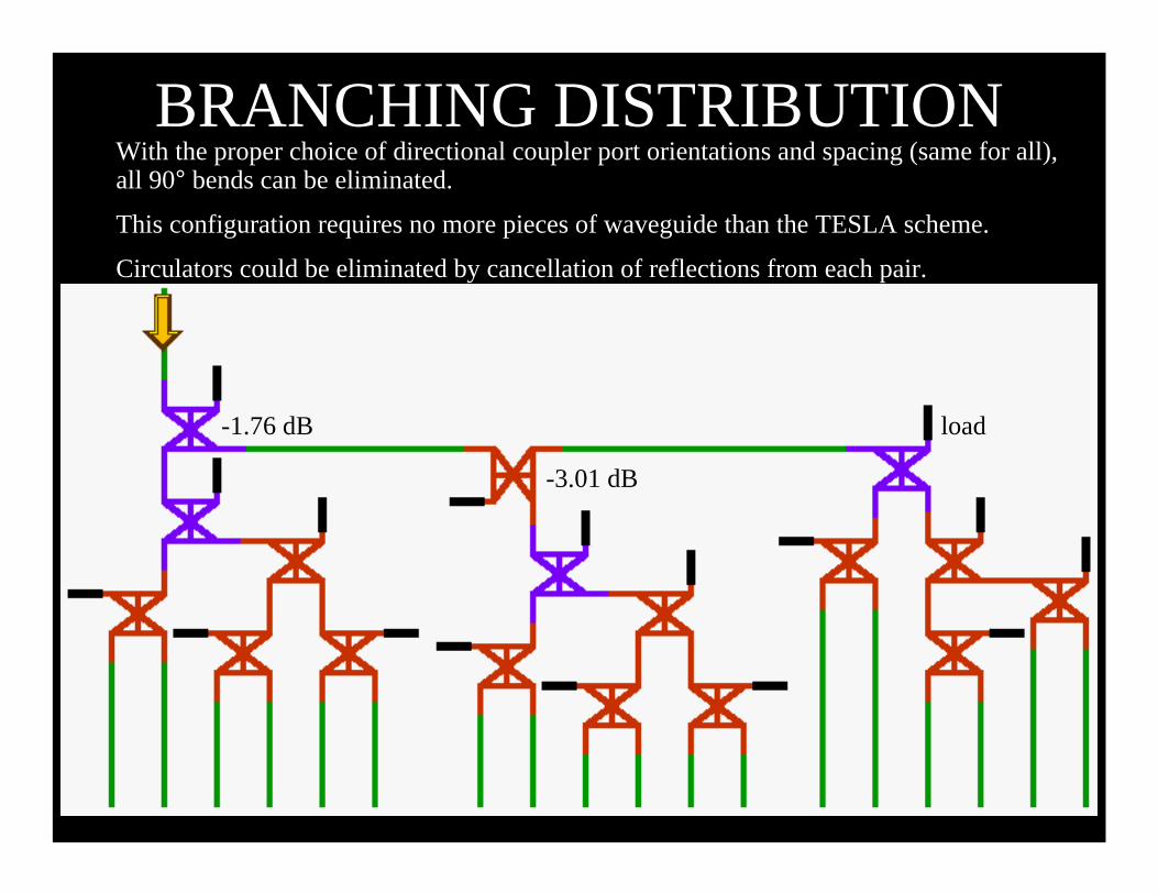
With the proper choice of directional coupler port orientations and spacing (same for all), all 90° bends can be eliminated.
This configuration requires no more pieces of waveguide than the TESLA scheme.
Circulators could be eliminated by cancellation of reflections from each pair.
-1.76 dB
-3.01 dB
load
BRANCHING DISTRIBUTION
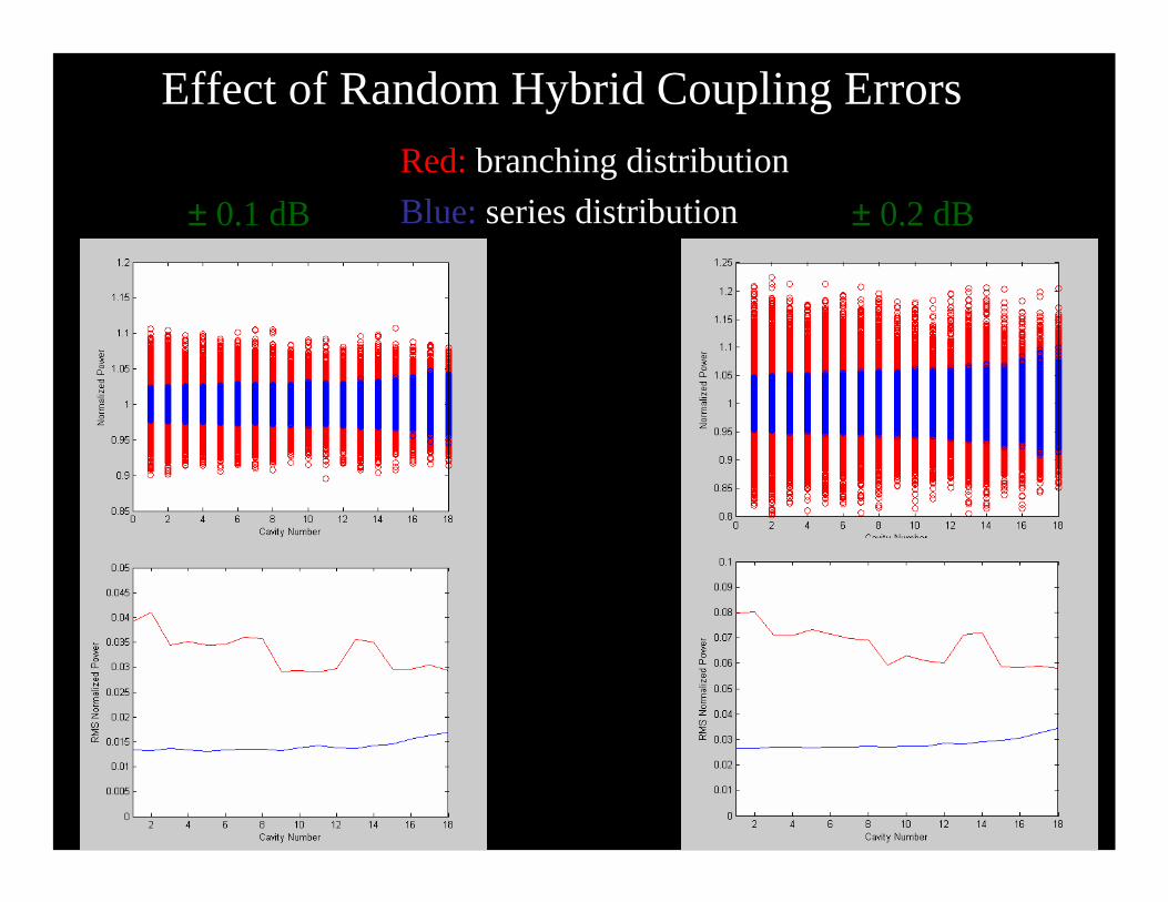
Effect of Random Hybrid Coupling ErrorsRed: branching distributionBlue: series distribution± 0.1 dB ± 0.2 dB
1000 runs
RUPAC ’02
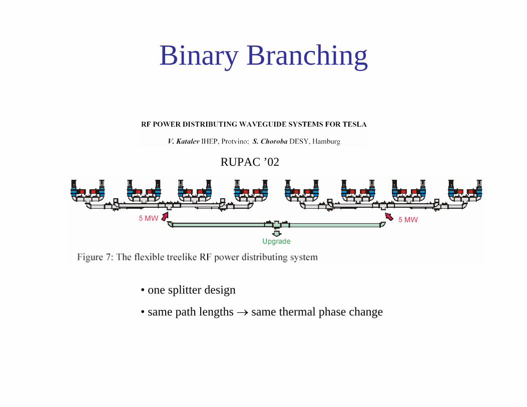
Binary Branching
• one splitter design
• same path lengths → same thermal phase change
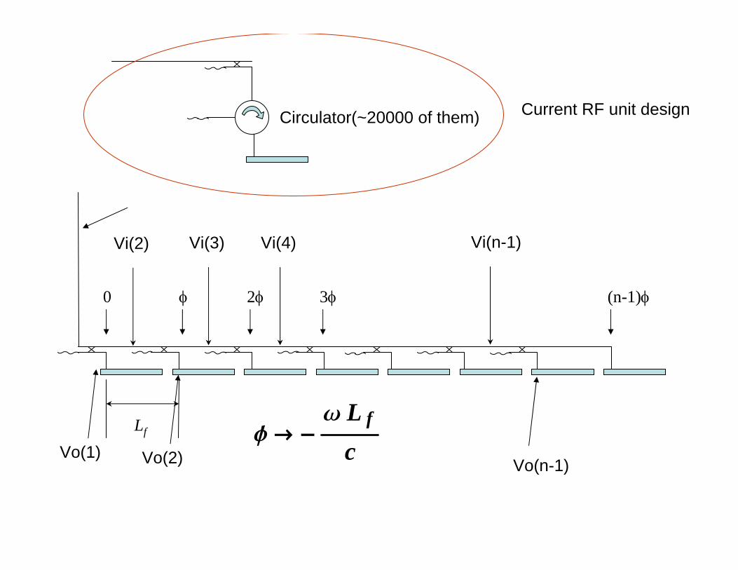
Lf f Æ -w L f
c
0 2φφ (n-1)φ3φ
Vi(2) Vi(3) Vi(4) Vi(n-1)
Vo(1) Vo(2) Vo(n-1)
Current RF unit designCirculator(~20000 of them)
1
2
3
4
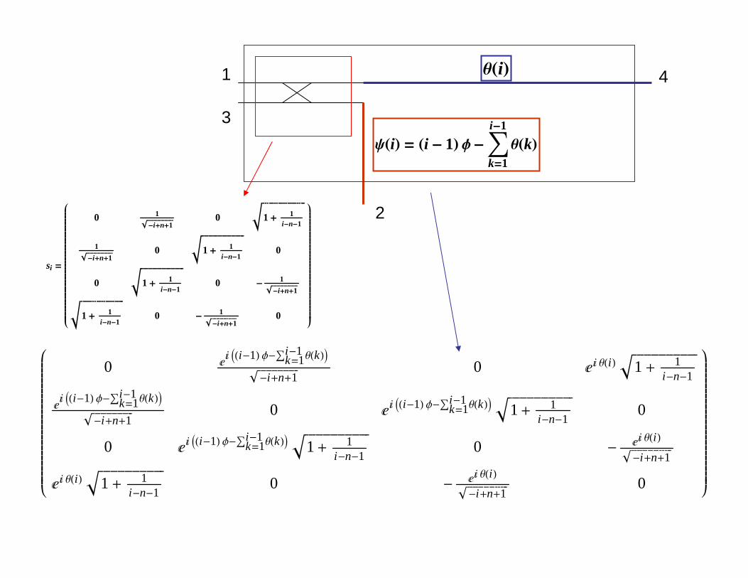
si =
i
k
jjjjjjjjjjjjjjjjjjjjjjjjjjjjjjjjjj
0 1è!!!!!!!!!!!!!!!-i+n+1
0 $%%%%%%%%%%%%%%%%%%%1 + 1i-n-1
1è!!!!!!!!!!!!!!!-i+n+1
0 $%%%%%%%%%%%%%%%%%%%1 + 1i-n-1
0
0 $%%%%%%%%%%%%%%%%%%%1 + 1i-n-1
0 - 1è!!!!!!!!!!!!!!!-i+n+1
$%%%%%%%%%%%%%%%%%%%1 + 1i-n-1
0 - 1è!!!!!!!!!!!!!!!-i+n+1
0
y
{
zzzzzzzzzzzzzzzzzzzzzzzzzzzzzzzzzz
i
k
jjjjjjjjjjjjjjjjjjjjjjjj
0 ‰Â IHi-1L f-⁄k=1i-1 qHkLM
è!!!!!!!!!!!!!!!-i+n+1
0 ‰Â qHiL "##################1 + 1i-n-1
‰Â IHi-1L f-⁄k=1i-1 qHkLM
è!!!!!!!!!!!!!!!-i+n+1
0 ‰Â IHi-1L f-⁄k=1i-1 qHkLM "##################1+ 1
i-n-10
0 ‰Â IHi-1L f-⁄k=1i-1 qHkLM "##################1+ 1
i-n-10 - ‰Â qHiLè!!!!!!!!!!!!!!!
-i+n+1
‰Â qHiL "##################1 + 1i-n-1
0 - ‰Â qHiLè!!!!!!!!!!!!!!!-i+n+10
y
{
zzzzzzzzzzzzzzzzzzzzzzzz
qHiL
yHiL = Hi - 1L f - ‚k=1
i-1
qHkL
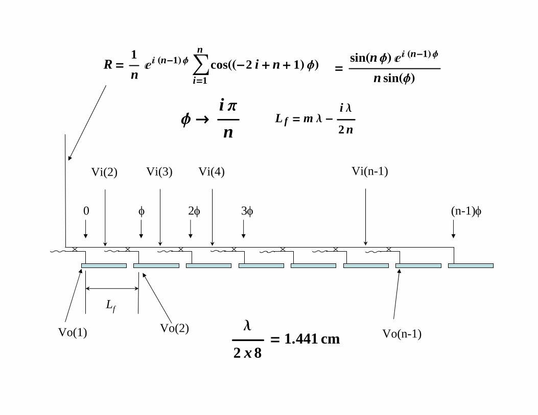
R =1n
„‰ Hn-1Lf ‚i=1
ncosHH-2 i + n + 1L fL =
sinHn fL „‰ Hn-1Lf
n sinHfL
f Æi p
n
Lf
0 2φφ (n-1)φ3φ
Vi(2) Vi(3) Vi(4) Vi(n-1)
Vo(2) Vo(n-1)Vo(1)
L f = m l -i l
2 n
l
2 x 8= 1.441 cm
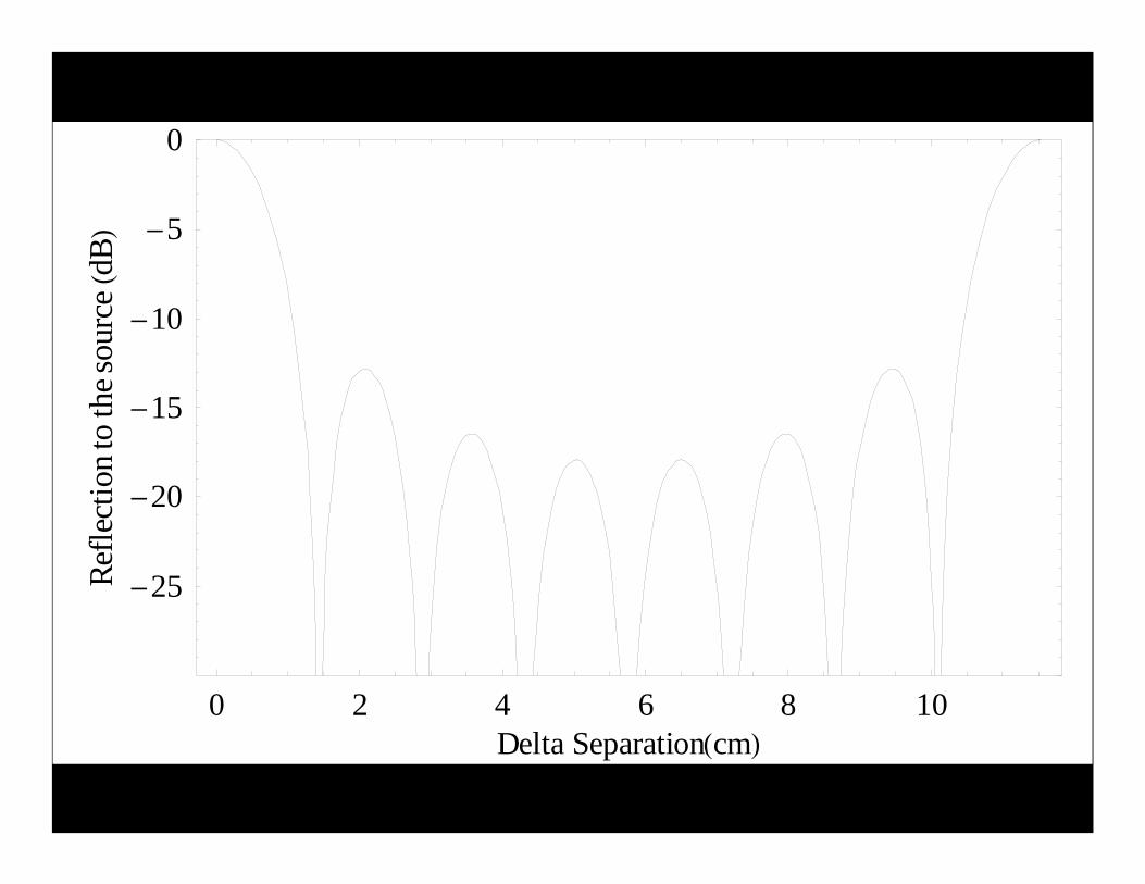
0 2 4 6 8 10Delta SeparationHcmL
-25
-20
-15
-10
-5
0noitcelfeR
oteht
ecruosHBd
L
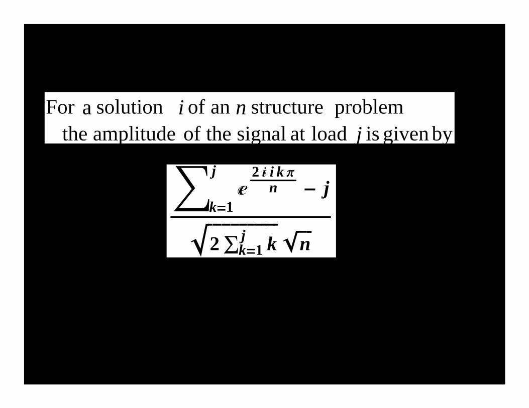
For a solution i of an n structure problemthe amplitude of the signal at load j is given by
k=1
j„
2 ‰ i k pn - j
2 k=1j k n
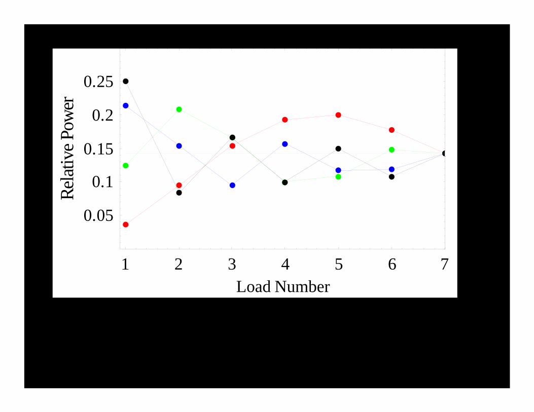
Distribution of power over the loads for different distribution solutions for 8 accelerator structures
1 2 3 4 5 6 7Load Number
0.05
0.1
0.15
0.2
0.25evitaleR
rewoP
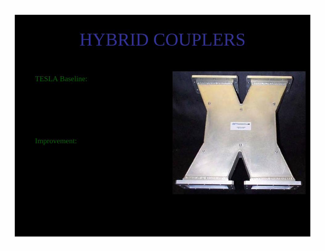
HYBRID COUPLERS
TESLA Baseline:• Manufactured by RFT SPINNER• -12.6 to -3.0 dB coupling (1/18 to 1/2)• coupling accuracy: ±0.2 dB• return loss 35 dB
Improvement:• tighten coupling accuracy to ±0.1dB• adjustable coupling?
(being investigated at DESY)

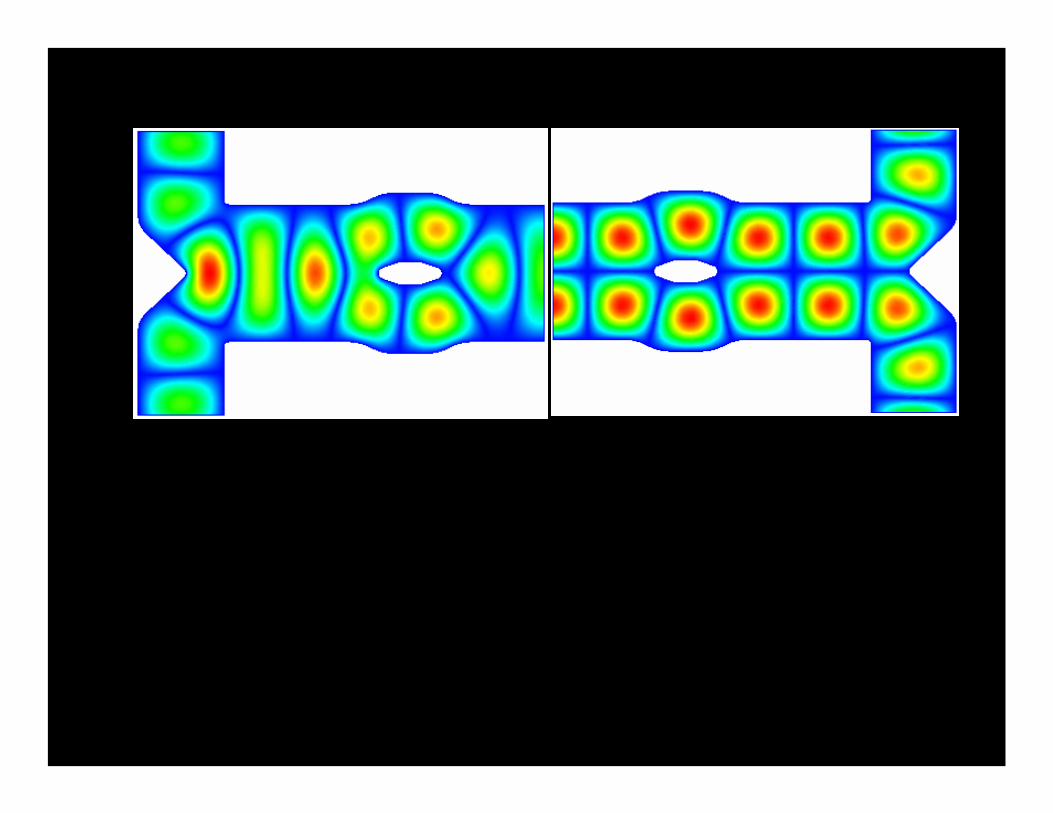
Dual-Mode CombinerTE10
TE20
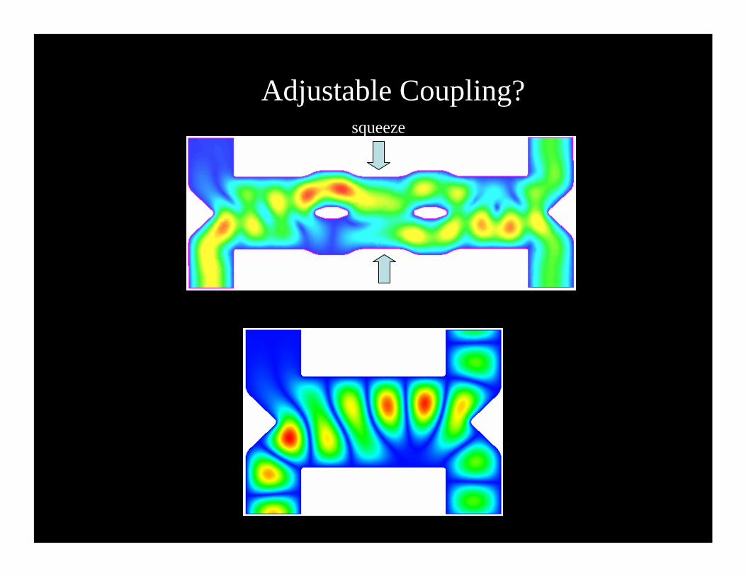
Adjustable Coupling?squeeze
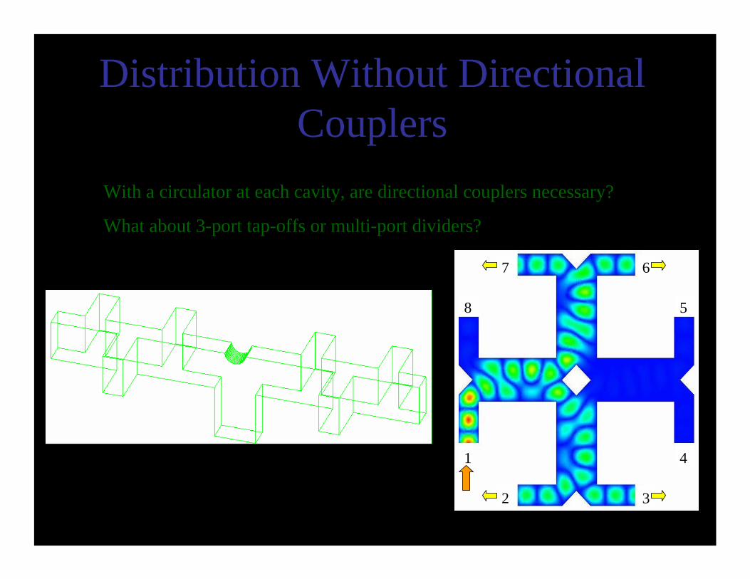
Distribution Without Directional Couplers
With a circulator at each cavity, are directional couplers necessary?
What about 3-port tap-offs or multi-port dividers?
1
2 3
4
5
67
8
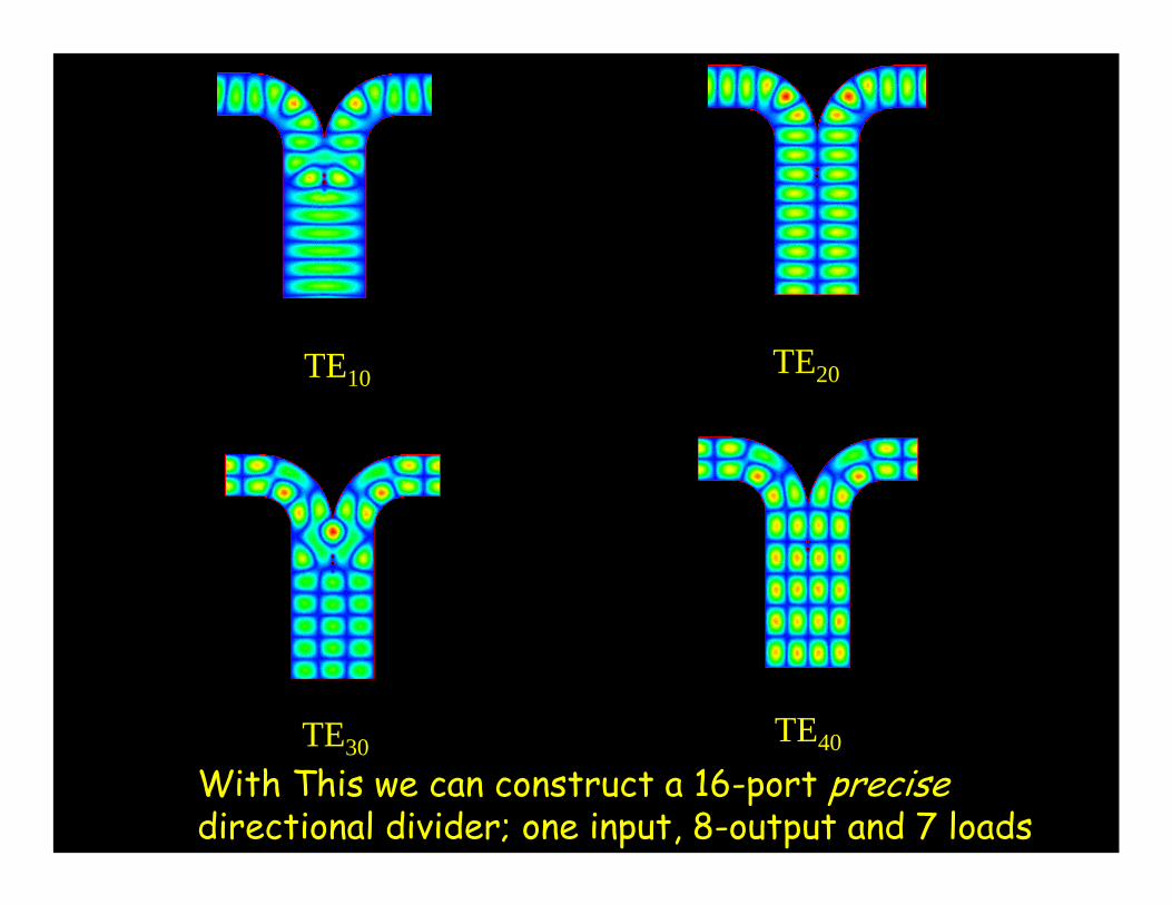
TE20TE10
TE30 TE40
With This we can construct a 16-port precisedirectional divider; one input, 8-output and 7 loads
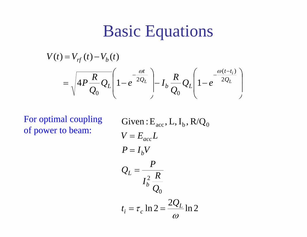
2ln22ln
R/Q ,IL,,E:Given
0
2
0bacc
ωτ L
ci
b
L
b
acc
Qt
QRI
PQ
VIPLEV
==
=
==
⎟⎟
⎠
⎞
⎜⎜
⎝
⎛−−
⎟⎟
⎠
⎞
⎜⎜
⎝
⎛−=
−=−
−−L
i
L Qtt
LbQ
t
L
brf
eQQRIeQ
QRP
tVtVtV
2)(
0
2
0114
)()()(ωω
For optimal coupling of power to beam:
Basic Equations
Va(Ib)Va(Prf)
Va(C)
Superconducting Cavity Behavior*
*Infinite Q0 assumed.
C∝Ee/Va∝Qe-1/2 assumed large enough that
Qe«Q0 but small enough that the initial reflection ≅ 1.
Dashed lines are for continually optimized coupling.
Ti(Prf)Ti(Ib)
Ti(C)
( )
( ) 0200
00
00
12)(
2)(
12)(
aa
ab
bba
arfrfrfa
VCCCC
CV
VIIIV
VPPPV
⎟⎟⎠
⎞⎜⎜⎝
⎛−=
⎟⎟⎠
⎞⎜⎜⎝
⎛−=
−=
( )( )[ ]
( ) ( )( )
00
2
30
20
00
00
2lnln112)(
ln1)(
ln2ln2
11)(
ii
ibbbi
irfrfrfi
TCCCCCC
CT
TIIIT
TPPPT
⎟⎠⎞
⎜⎝⎛ +⎟
⎟⎠
⎞⎜⎜⎝
⎛−=
−=
⎥⎦⎤
⎢⎣⎡ +=
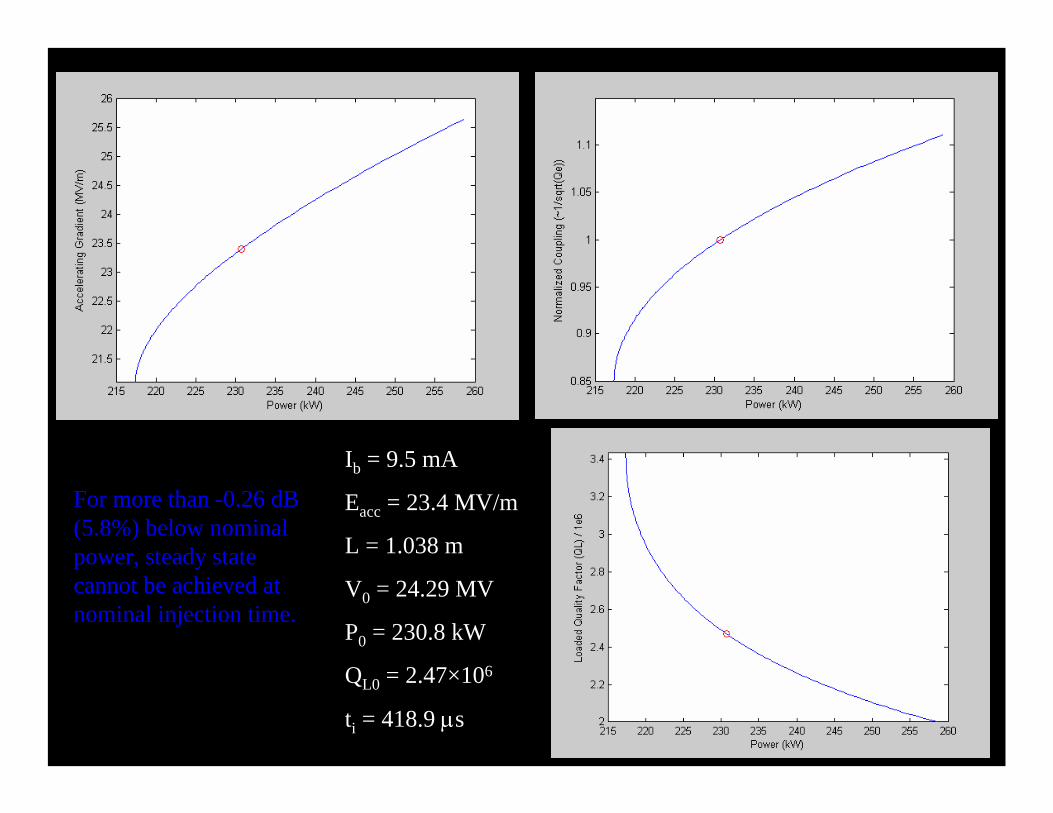
For more than -0.26 dB (5.8%) below nominal power, steady state cannot be achieved at nominal injection time.
Ib = 9.5 mA
Eacc = 23.4 MV/m
L = 1.038 m
V0 = 24.29 MV
P0 = 230.8 kW
QL0 = 2.47×10⁶
ti = 418.9 µs
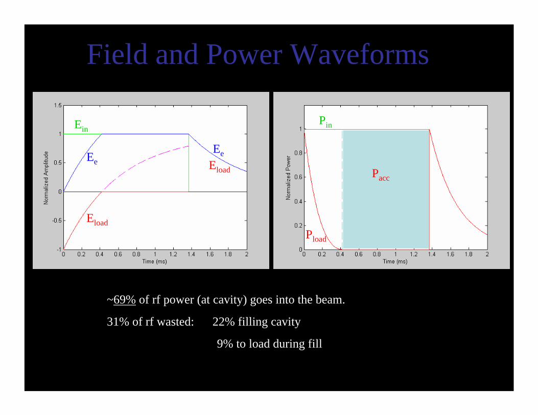
~69% of rf power (at cavity) goes into the beam.
31% of rf wasted: 22% filling cavity
9% to load during fill
Pin
Pload
Pacc
Ein
Ee
Eload
Eload
Ee
( )2/12ln −= cinL Pfill
τE
Field and Power Waveforms
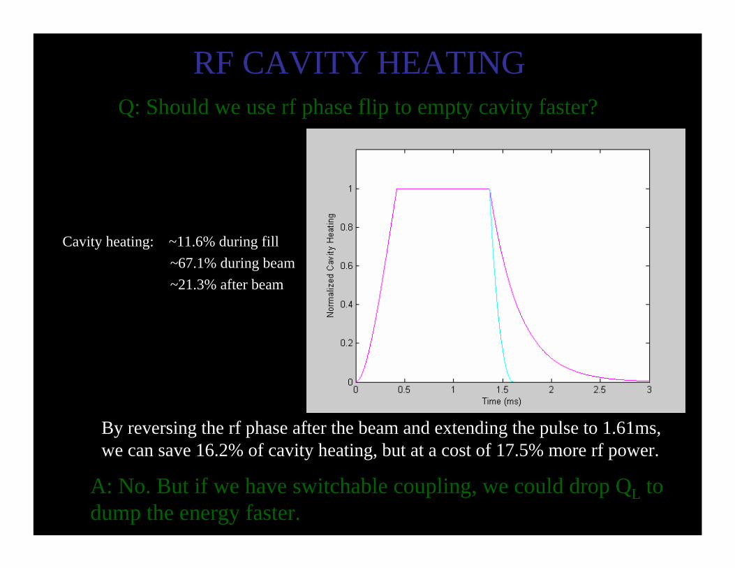
Cavity heating: ~11.6% during fill~67.1% during beam~21.3% after beam
By reversing the rf phase after the beam and extending the pulse to 1.61ms, we can save 16.2% of cavity heating, but at a cost of 17.5% more rf power.
RF CAVITY HEATINGQ: Should we use rf phase flip to empty cavity faster?
A: No. But if we have switchable coupling, we could drop QL to dump the energy faster.
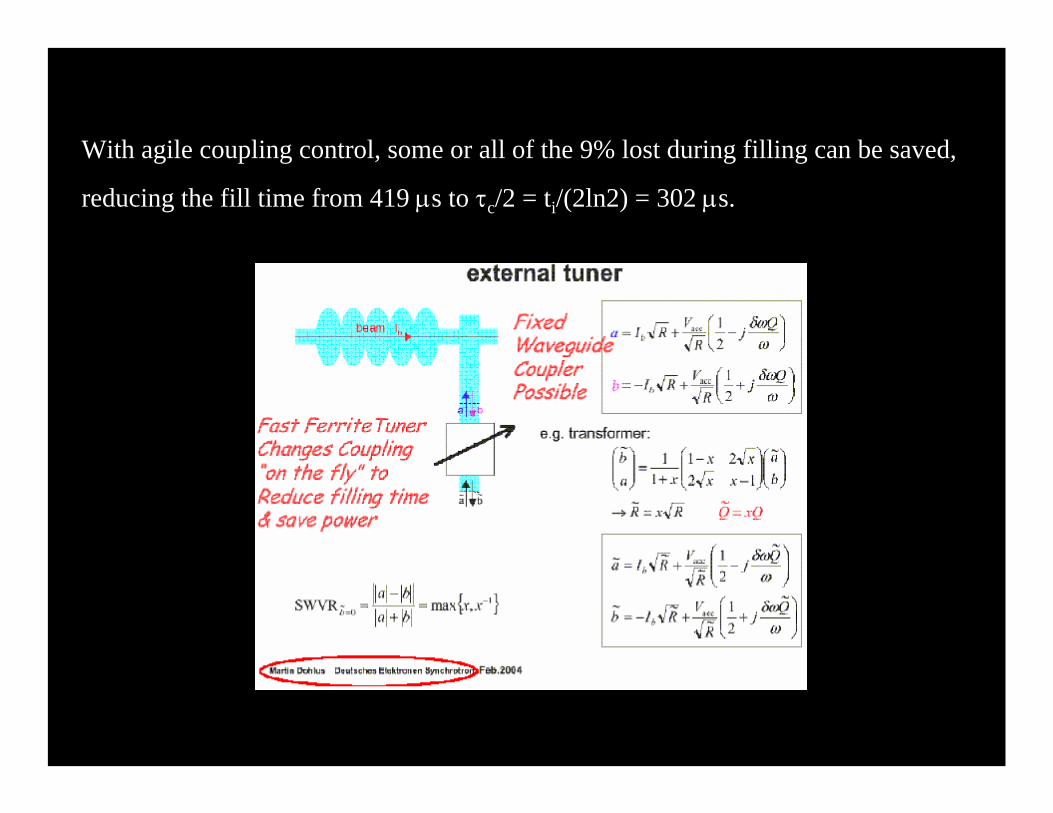
With agile coupling control, some or all of the 9% lost during filling can be saved,
reducing the fill time from 419 µs to τc/2 = ti/(2ln2) = 302 µs.
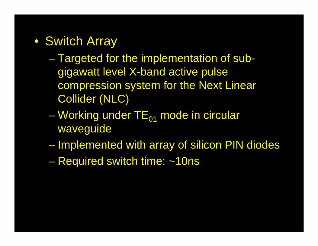
• Switch Array– Targeted for the implementation of sub-
gigawatt level X-band active pulse compression system for the Next Linear Collider (NLC)
– Working under TE01 mode in circular waveguide
– Implemented with array of silicon PIN diodes– Required switch time: ~10ns
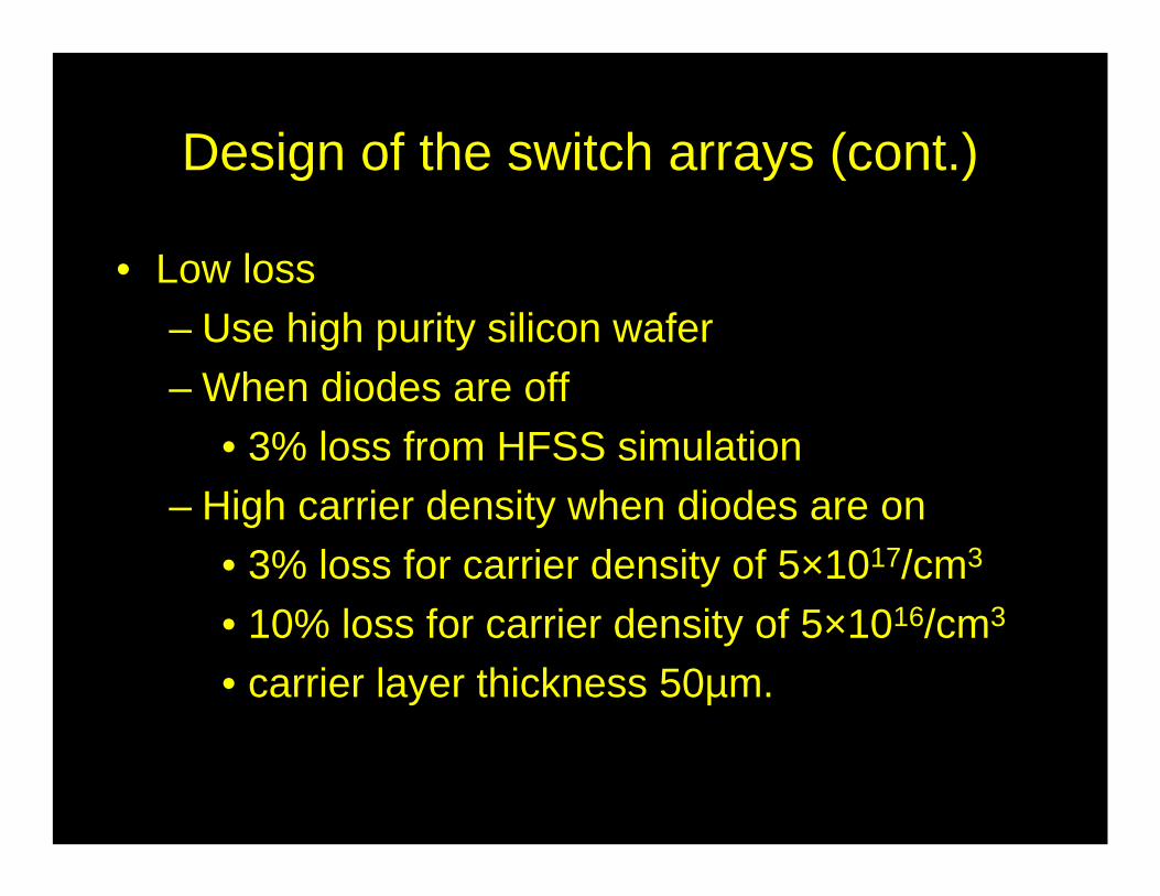
Design of the switch arrays (cont.)
• Low loss– Use high purity silicon wafer– When diodes are off
• 3% loss from HFSS simulation– High carrier density when diodes are on
• 3% loss for carrier density of 5×10¹⁷/cm3
• 10% loss for carrier density of 5×10¹⁶/cm3
• carrier layer thickness 50µm.
Introduction (cont.)• Amplifier array– Potential megawatt level pulsed RF source– Similar configuration as the switch array– Implemented with silicon IMPATT diodes– Output of diodes are spatially combined– Other device/material options
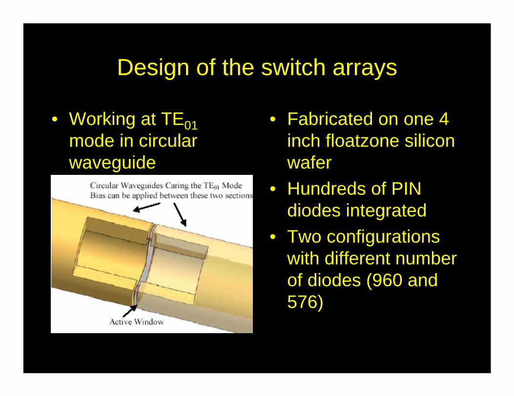
Design of the switch arrays
• Working at TE01mode in circular waveguide
• Fabricated on one 4 inch floatzone silicon wafer
• Hundreds of PIN diodes integrated
• Two configurations with different number of diodes (960 and 576)
Design and Implementation of PIN/NIP DiodeArray Active Window
PIN diode array Active Window• All doping profile and metallic terminals on the window are
radial, i.e. perpendicular to electric field of the TE01 mode. Effect of doping and metal lines on RF signal is small when thediode is reverse biased.
• With forward bias, carriers are injected into I region and I regionbecomes conductor RF signal is reflected.
P
N N
side view(not to scale) metal line (1.5um thick)
I
~10um
• Base material: high resistivity (pure) silicon, <5000ohm-cm, n-type
• Diameter of active region: 1.3 inch• Thickness: 220um• Coverage (metal/doping line on the surface): ~10%
Metal terminal
Radial-line PIN diode arraystructure (400 lines)
220um
2 inch
A B
Section A--B
RF structure• DC isolation by Al2O3 ceramic ring• No RF choke is needed (TE01 mode)• Higher impedance (Zg / Z0 ~4, close to cutoff) for this
experimento Enhance the effect of window switching statuso Lower loss at the window during forward biaso Huge mismatch without bias
Ceramic ring for DC isolationActive PIN/NIP diode window
2”
Metal spring for DC contactbetween RF structure and theactive window
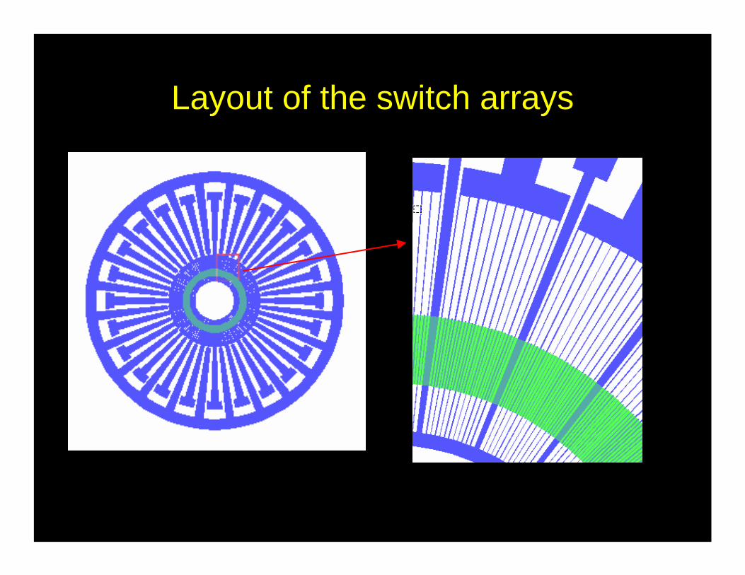
Layout of the switch arrays
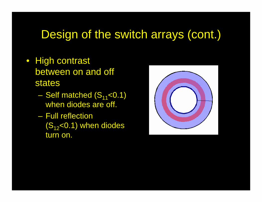
Design of the switch arrays (cont.)
• High contrast between on and off states– Self matched (S11<0.1)
when diodes are off.– Full reflection
(S12<0.1) when diodes turn on.
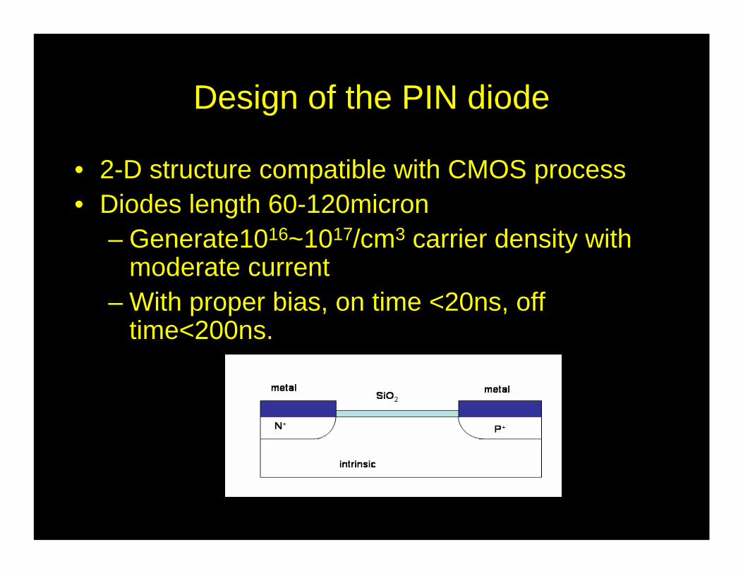
Design of the PIN diode
• 2-D structure compatible with CMOS process• Diodes length 60-120micron
– Generate1016~1017/cm3 carrier density with moderate current
– With proper bias, on time <20ns, off time<200ns.
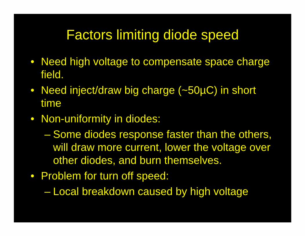
Factors limiting diode speed
• Need high voltage to compensate space charge field.
• Need inject/draw big charge (~50µC) in short time
• Non-uniformity in diodes:– Some diodes response faster than the others,
will draw more current, lower the voltage over other diodes, and burn themselves.
• Problem for turn off speed:– Local breakdown caused by high voltage

Fabrication of the diode array
• Fabricated at Stanford Nanofabrication Facility
• Using CMOS compatible technology
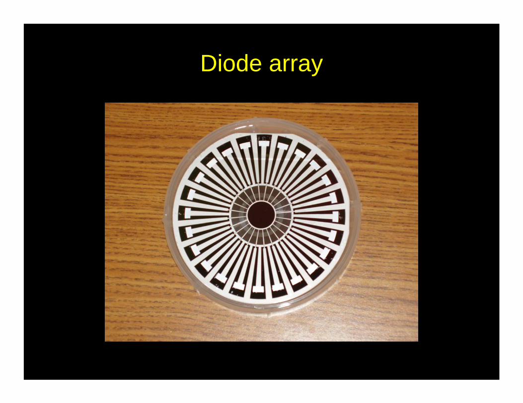
Diode array
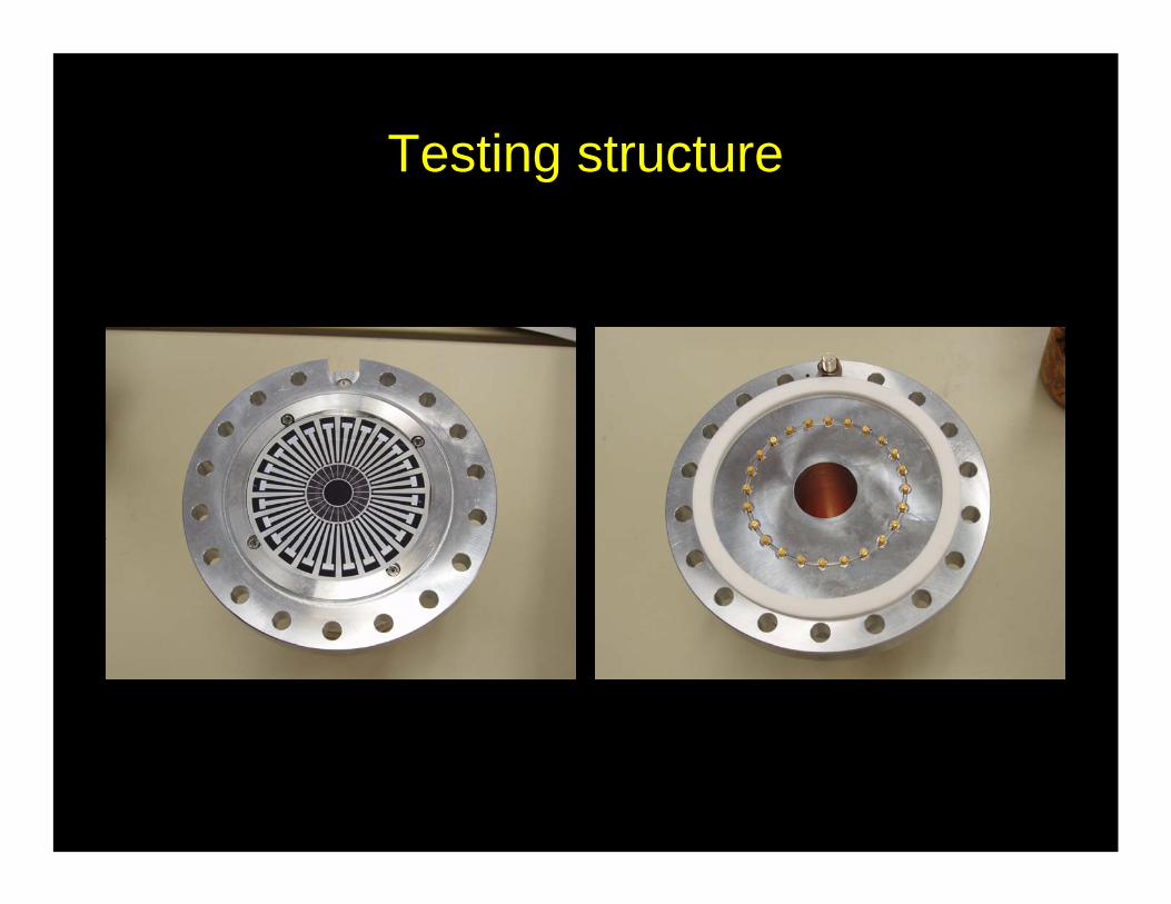
Testing structure
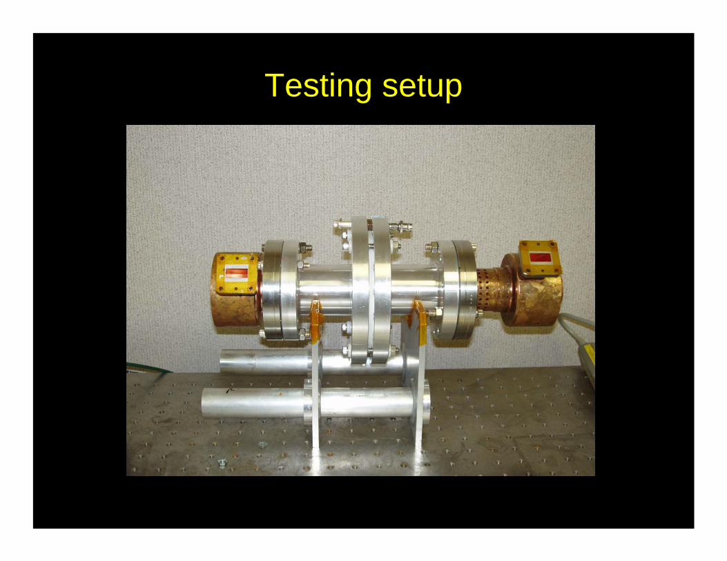
Testing setup
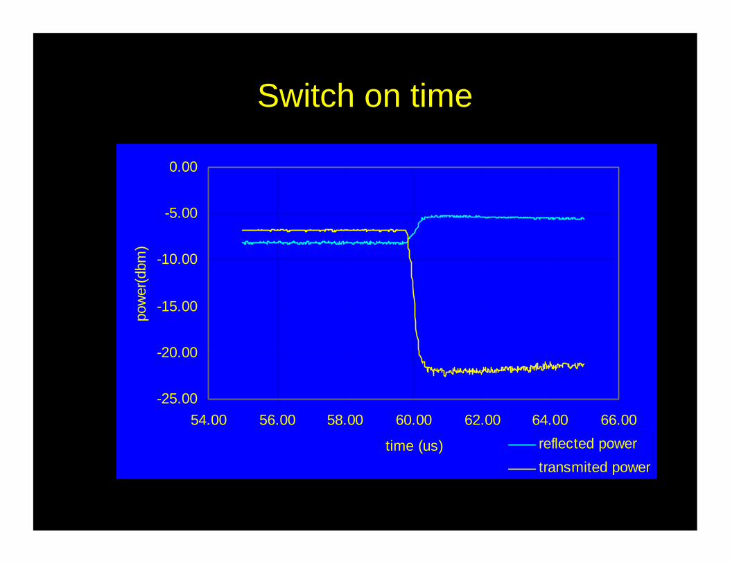
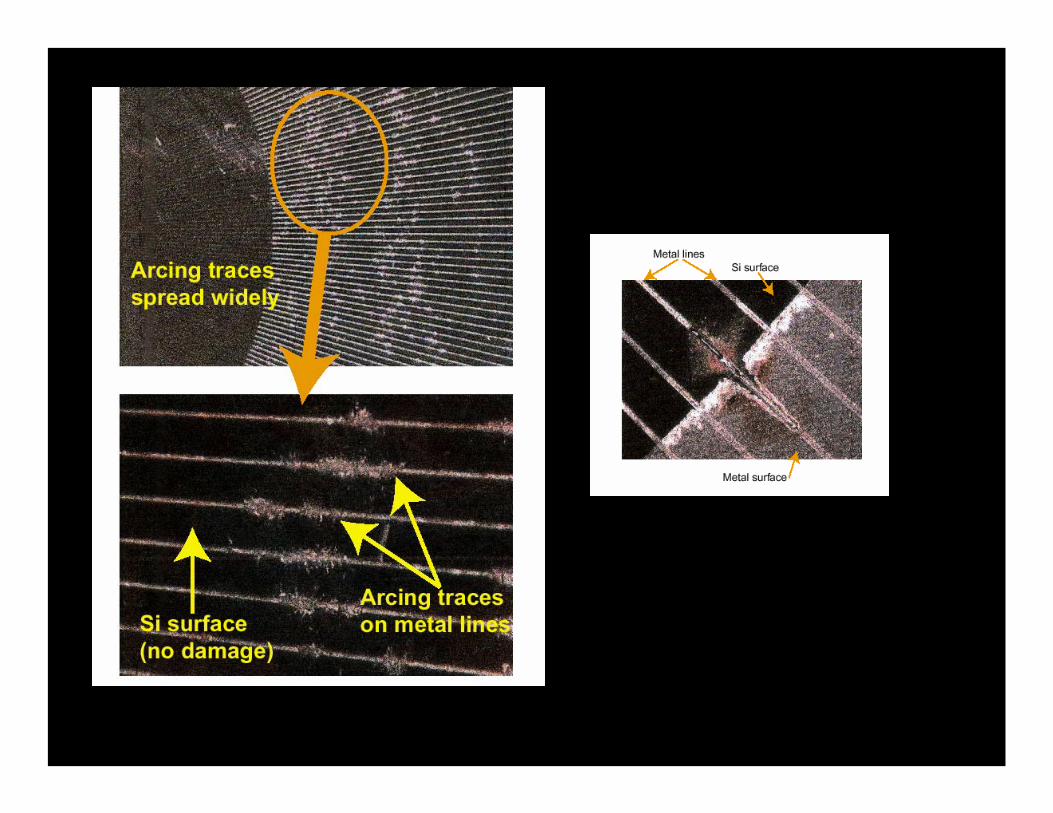
Switch on time
-25.00
-20.00
-15.00
-10.00
-5.00
0.00
54.00 56.00 58.00 60.00 62.00 64.00 66.00
time (us)
pow
er(d
bm)
reflected powertransmited power
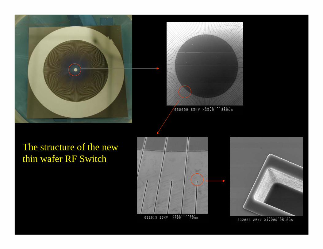
The structure of the new thin wafer RF Switch
Port 2 (rf)
Port 1 (rf)
Port A (Bias)
Garnet Material
Wrap-around Mode converter
Coaxial TE01and TE02 mode
propagate in this coaxial structure
Port 3 (rf)
Port 2 (rf)
Port 1 (rf)
Port A (Bias)
Garnet Material
Wrap-around Mode converter
Coaxial TE01and TE02 mode
propagate in this coaxial structure
Port 3 (rf)
Port B (Bias)
Port 1 (rf) Port 2 (rf)
Port A (Bias)
Garnet Material
Wrap-around Mode
converter
Coaxial TE01 mode propagate in this coaxial
structure
Port B (Bias)
Port 1 (rf) Port 2 (rf)
Port A (Bias)
Garnet Material
Wrap-around Mode
converter
Coaxial TE01 mode propagate in this coaxial
structurePort 1 (rf) Port 2 (rf)
Port A (Bias)
Garnet Material
Wrap-around Mode
converter
Coaxial TE01 mode propagate in this coaxial
structure
Wrap-Around Mode Converter for Tap-off, and extraction, tested to 470 MW
rg
ri
ro
Garnet Material
r
x
y
z
φ
Biasing magnetic field
rg
ri
ro
Garnet Material
r
x
y
z
φ
Biasing magnetic field
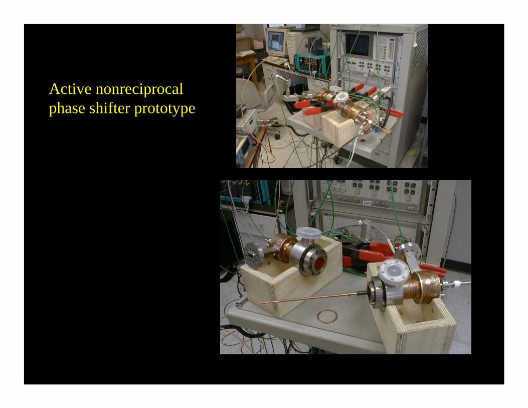
Active nonreciprocal phase shifter prototype
100
120
140
160
180
200
220
240
11.1 11.2 11.3 11.4 11.5 11.6 11.7
Phase difference between forward and backward waves
Phas
e di
ffere
nce
betw
een
forw
ard
and
back
war
d w
aves
Freq GHz
0
0.2
0.4
0.6
0.8
1
11.1 11.2 11.3 11.4 11.5 11.6 11.7
Matched Nonreciprocal Overmoded Phase Shifter
S11
S12
S21
S22
Dat
a M
ag
Freq GHz
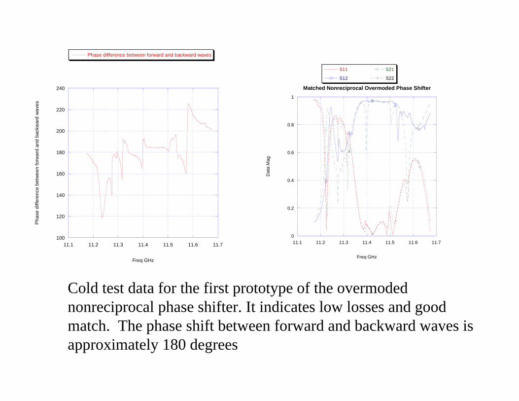
Cold test data for the first prototype of the overmoded nonreciprocal phase shifter. It indicates low losses and good match. The phase shift between forward and backward waves is approximately 180 degrees
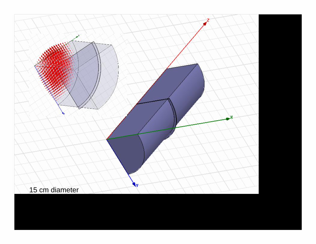
15 cm diameter1 mm gap (vacuum)The waveguide is Al2O3 RodTE01 Mode
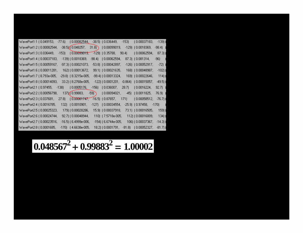
0.0485672 + 0.998832 = 1.00002
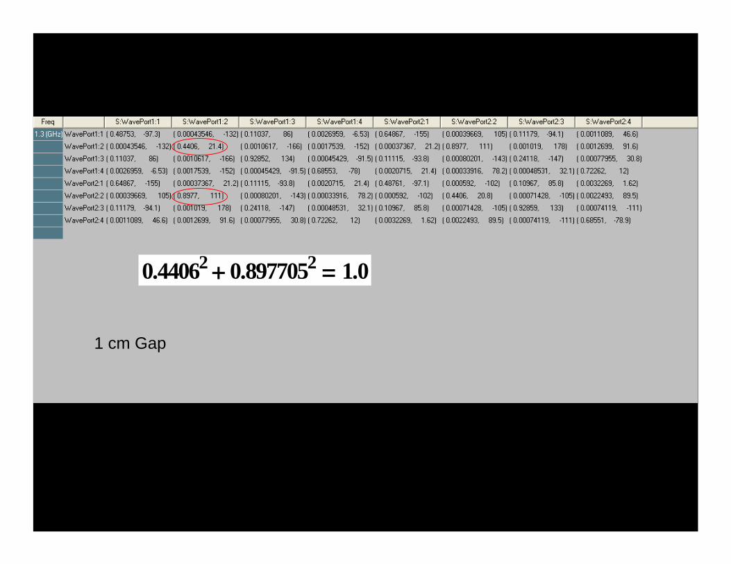
1 cm Gap
0.44062 + 0.8977052 = 1.0
-46.3 dB suppression of TE11 relative to TM01 at end of 10 cm beampipe.
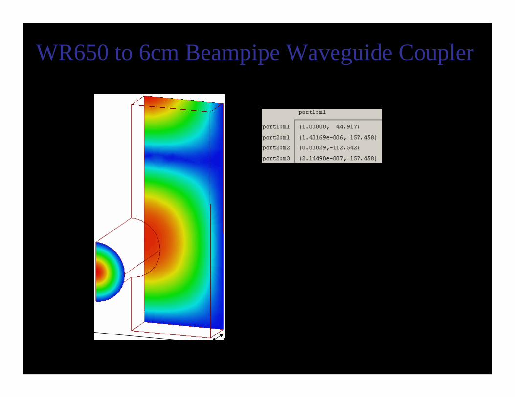
D = 6.0 cm
a = 6.500” = 16.51cm b = 3.6275 cm
h = 8.4652 cm
WR650 to 6cm Beampipe Waveguide Coupler
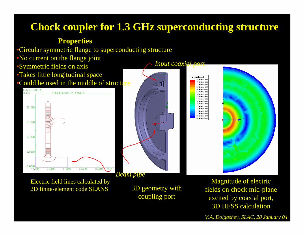
Chock coupler for 1.3 GHz superconducting structureProperties
•Circular symmetric flange to superconducting structure •No current on the flange joint•Symmetric fields on axis•Takes little longitudinal space•Could be used in the middle of structure
Electric field lines calculated by 2D finite-element code SLANS 3D geometry with
coupling port
Beam pipe
Input coaxial port
Magnitude of electric fields on chock mid-plane
excited by coaxial port, 3D HFSS calculation
V.A. Dolgashev, SLAC, 28 January 04
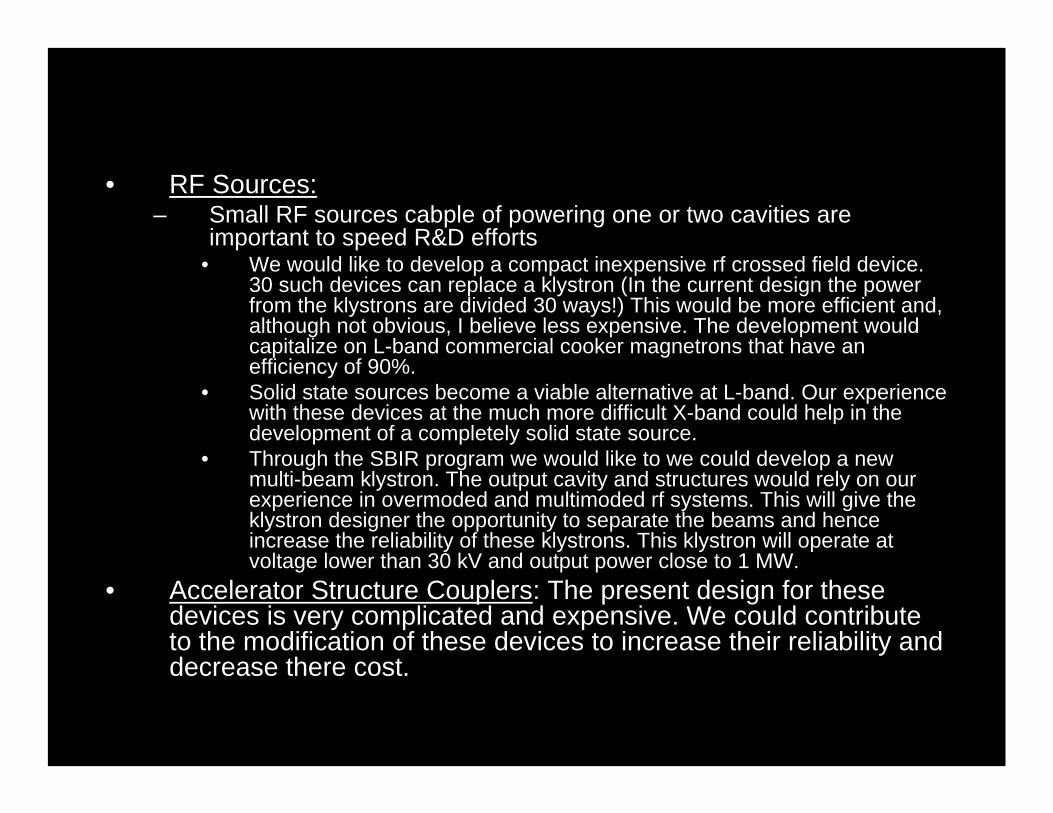
Suggested Future activities
• RF Sources:– Small RF sources cabple of powering one or two cavities are
important to speed R&D efforts• We would like to develop a compact inexpensive rf crossed field device.
30 such devices can replace a klystron (In the current design the power from the klystrons are divided 30 ways!) This would be more efficient and, although not obvious, I believe less expensive. The development would capitalize on L-band commercial cooker magnetrons that have an efficiency of 90%.
• Solid state sources become a viable alternative at L-band. Our experience with these devices at the much more difficult X-band could help in the development of a completely solid state source.
• Through the SBIR program we would like to we could develop a newmulti-beam klystron. The output cavity and structures would rely on our experience in overmoded and multimoded rf systems. This will give the klystron designer the opportunity to separate the beams and hence increase the reliability of these klystrons. This klystron will operate at voltage lower than 30 kV and output power close to 1 MW.
• Accelerator Structure Couplers: The present design for these devices is very complicated and expensive. We could contribute to the modification of these devices to increase their reliability and decrease there cost.
•By Relating spacing of cavities to the RF distribution system it is possible to eliminate about 20000 Circulator ($20 M to $200 M) without any clear draw backs
•One should think about the main linac as a system. The separation of the development of the RF sources from the modulators from the distribution system from the power couplers from linac / cryogenic module development will result in lost opportunities
•Spatially combined RF devices can provide RF sources. It can also provide switches to enhance the charging and discharging of the cavities, i.e., active couplers.
Conclusion