Embed Size (px)
Citation preview
SAM4E Microcontrollers
SAM4E-EK Evaluation Kit
USER GUIDE
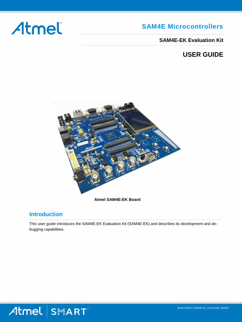
Atmel SAM4E-EK Board
Introduction
This user guide introduces the SAM4E-EK Evaluation Kit (SAM4E-EK) and describes its development and de-
bugging capabilities.
Atmel-42067C-SAM4E-EK_UserGuide_022016
SAM4E-EK Evaluation Kit [USER GUIDE] Atmel-42067C-SAM4E-EK_UserGuide_022016 2
2
Table of Contents
1 Introduction .................................................................................................................. 3
1.1 User Guide ............................................................................................................................................ 3
1.2 References and Applicable Documents................................................................................................. 3
2 Kit Contents ................................................................................................................. 3
2.1 Deliverables ........................................................................................................................................... 3
2.2 Electrostatic Warning ............................................................................................................................ 4
3 Power Up ..................................................................................................................... 5
3.1 Power Up the Board .............................................................................................................................. 5
3.2 Source Code and Technical Support ..................................................................................................... 5
4 Board Description ........................................................................................................ 6
4.1 Board Overview ..................................................................................................................................... 6
4.2 Features List .......................................................................................................................................... 7
4.3 Function Blocks ..................................................................................................................................... 7
4.3.1 Processor ................................................................................................................................. 7
4.3.2 Memory ..................................................................................................................................... 7
4.3.3 Clock Circuitry ........................................................................................................................... 8
4.3.4 Reset Circuitry .......................................................................................................................... 9
4.3.5 Power Supply and Management ............................................................................................... 9
4.3.6 UART ...................................................................................................................................... 11
4.3.7 USART ................................................................................................................................... 11
4.3.8 RS485 ..................................................................................................................................... 12
4.3.9 Ethernet MAC 10/100 (EMAC)................................................................................................ 13
4.3.10 CAN ........................................................................................................................................ 13
4.3.11 Display Interface ..................................................................................................................... 14
4.3.12 Touch Screen Interface .......................................................................................................... 16
4.3.13 JTAG/ICE ............................................................................................................................... 16
4.3.14 Audio Interface........................................................................................................................ 17
4.3.15 USB Device ............................................................................................................................ 18
4.3.16 Analog Interface ...................................................................................................................... 18
4.3.16.1 Analog Reference ................................................................................................... 18
4.3.16.2 Analog Input ............................................................................................................ 19
4.3.16.3 Analog Output ......................................................................................................... 20
4.3.17 QTouch Elements ................................................................................................................... 20
4.3.18 LEDs ....................................................................................................................................... 21
4.3.19 SD/MMC Card ........................................................................................................................ 21
4.3.20 ZigBee .................................................................................................................................... 22
4.3.21 PIO Expansion ........................................................................................................................ 22
5 Configuration ............................................................................................................. 24
5.1 PIO Usage ........................................................................................................................................... 24
5.2 Jumpers .............................................................................................................................................. 27
6 Schematics ................................................................................................................. 29
7 ATMEL EVALUATION BOARD/KIT IMPORTANT NOTICE AND DISCLAIMER ........ 38
8 Revision History ........................................................................................................ 39
SAM4E-EK Evaluation Kit [USER GUIDE] Atmel-42067C-SAM4E-EK_UserGuide_022016
3
3
1 Introduction
1.1 User Guide
This user guide gives details on how the Atmel® SAM4E-EK has been designed. It is made up of six
chapters:
Chapter 1 includes references, applicable documents
Chapter 2 describes the kit contents, ESD warnings
Chapter 3 provides instructions to power up the SAM4E-EK and technical support
Chapter 4 describes overview, feature list, the hardware resources including the schematics
Chapter 5 provides configurations and jumper settings
Chapter 6 provides the entire board schematics
1.2 References and Applicable Documents
Table 1-1. References and Applicable Documents
Reference Title Comment
Lit. no.: 11157 SAM4E datasheet www.atmel.com
2 Kit Contents
2.1 Deliverables
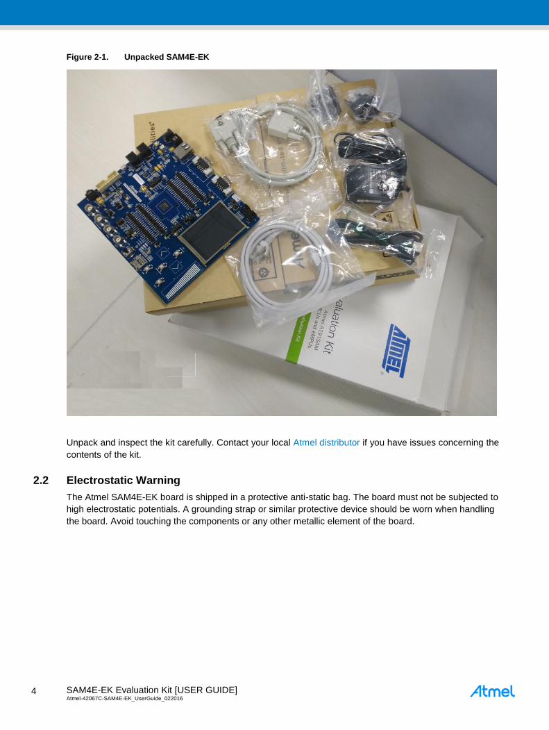
The Atmel SAM4E-EK toolkit contains the following items:
An Atmel SAM4E-EK board
Power supply
Universal input AC/DC power supply with US, Europe, and UK plug adapters
One USB cable
One serial RS232 cable
One Ethernet cross cable
A welcome letter
SAM4E-EK Evaluation Kit [USER GUIDE] Atmel-42067C-SAM4E-EK_UserGuide_022016 4
4
Figure 2-1. Unpacked SAM4E-EK
Unpack and inspect the kit carefully. Contact your local Atmel distributor if you have issues concerning the
contents of the kit.
2.2 Electrostatic Warning
The Atmel SAM4E-EK board is shipped in a protective anti-static bag. The board must not be subjected to
high electrostatic potentials. A grounding strap or similar protective device should be worn when handling
the board. Avoid touching the components or any other metallic element of the board.
SAM4E-EK Evaluation Kit [USER GUIDE] Atmel-42067C-SAM4E-EK_UserGuide_022016
5
5
3 Power Up
3.1 Power Up the Board
Unpack the board taking care to avoid electrostatic discharge. Unpack the power supply, select the right
power plug adapter corresponding to that of your country, and insert it into the power supply.
Connect the power supply DC connector to the board and plug the power supply to an AC power socket.
The board LCD should light up and display a welcome page. Then click or touch the icons displayed on
the screen and enjoy the demo.
3.2 Source Code and Technical Support
After boot up, you can run some sample code or your own application on the development kit. You can
download sample code and get technical support from the Atmel web site: http://www.atmel.com.
SAM4E-EK Evaluation Kit [USER GUIDE] Atmel-42067C-SAM4E-EK_UserGuide_022016 6
6
4 Board Description
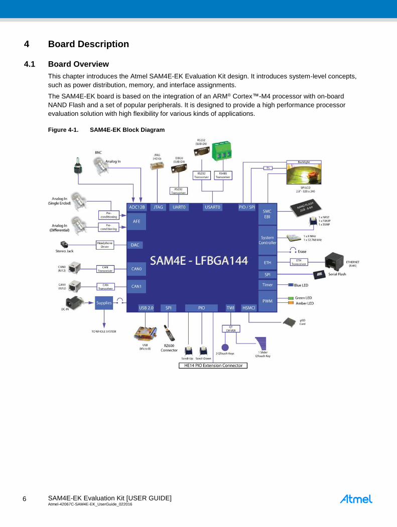
4.1 Board Overview
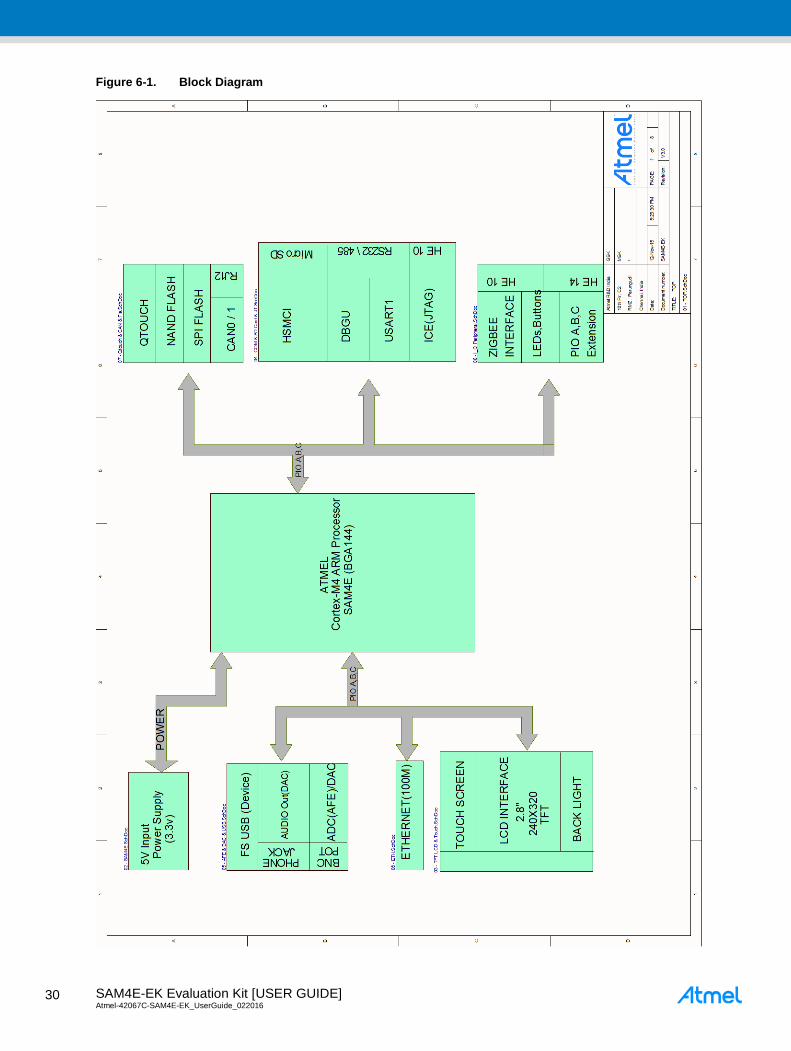
This chapter introduces the Atmel SAM4E-EK Evaluation Kit design. It introduces system-level concepts,
such as power distribution, memory, and interface assignments.
The SAM4E-EK board is based on the integration of an ARM® Cortex™-M4 processor with on-board
NAND Flash and a set of popular peripherals. It is designed to provide a high performance processor
evaluation solution with high flexibility for various kinds of applications.
Figure 4-1. SAM4E-EK Block Diagram
SAM4E-EK Evaluation Kit [USER GUIDE] Atmel-42067C-SAM4E-EK_UserGuide_022016
7
7
4.2 Features List
The main board components and interfaces:
SAM4E16 chip BGA144 package with optional socket footprint
12MHz crystal
32.768kHz crystal
Optional SMB connector for external system clock input
NAND Flash
2.8 inch TFT color LCD display with touch panel and backlight
UART port with RS232 driver
USART port with RS232 driver multiplexed with RS485 function with driver
CAN port with driver
Mono/stereo headphone jack output
One Ethernet physical transceiver layer with RJ45 connector
SD/MMC interface
Reset button: NRST
User buttons: WAKU, TAMP, Scroll-up, and Scroll-down
QTouch® buttons: Left, Right, and Slider
Full Speed USB device port
JTAG/ICE port
On-board power regulation
Three user LEDs
Power LED
BNC connector for ADC input
BNC connector for DAC output
User potentiometer connected to the ADC input
ZigBee® connector
PIO connection interfaces (PIOA, PIOC and PIOD with 32-bit, PIOB with 16-bit, and PIOE with 6-
bit)
4.3 Function Blocks
4.3.1 Processor
The Atmel SAM4E-EK is equipped with a SAM4E16 device in BGA144 package.
4.3.2 Memory
The SAM4E16 chip embeds:
1024kB of embedded Flash
128kB of embedded SRAM
16kB of ROM with embedded boot loader routines (UART, USB) and In-Application Programming
functions (IAP) routines
The SAM4E16 features an External Bus Interface (EBI) that permits interfacing to a broad range of
external memories and virtually to any parallel peripheral.
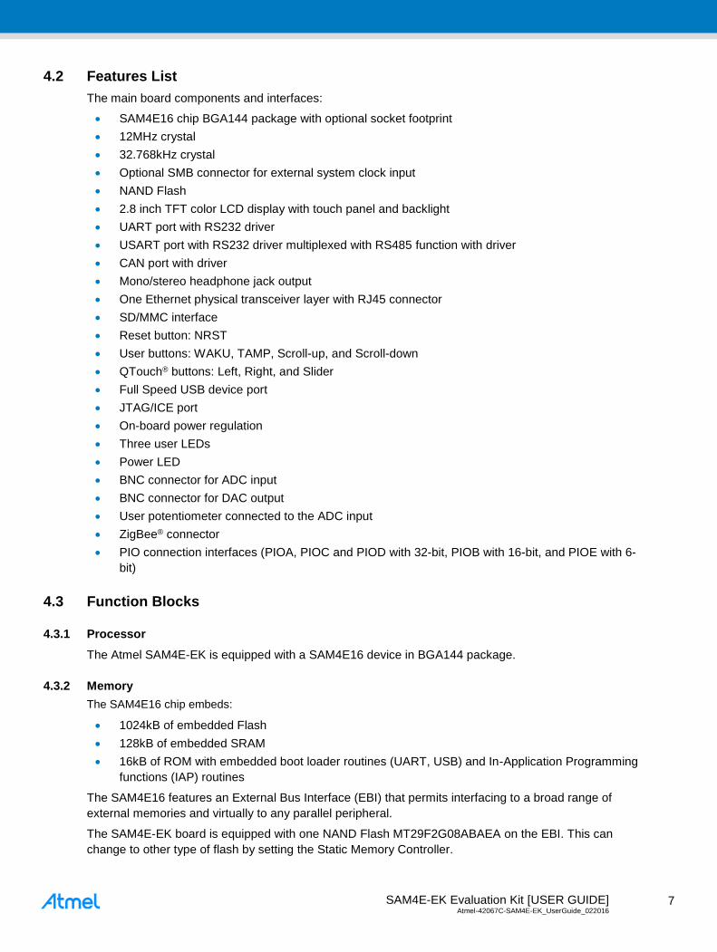
The SAM4E-EK board is equipped with one NAND Flash MT29F2G08ABAEA on the EBI. This can
change to other type of flash by setting the Static Memory Controller.
SAM4E-EK Evaluation Kit [USER GUIDE] Atmel-42067C-SAM4E-EK_UserGuide_022016 8
8
Figure 4-2. NAND-Flash
NCS0 chip select signal is used for NAND Flash chip selection. Furthermore, a dedicated jumper can
disconnect it from the on-board memories, thereby letting NCS0 free for other custom purposes.
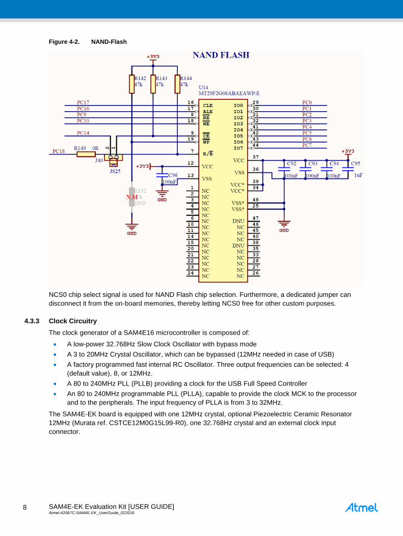
4.3.3 Clock Circuitry
The clock generator of a SAM4E16 microcontroller is composed of:
A low-power 32.768Hz Slow Clock Oscillator with bypass mode
A 3 to 20MHz Crystal Oscillator, which can be bypassed (12MHz needed in case of USB)
A factory programmed fast internal RC Oscillator. Three output frequencies can be selected: 4
(default value), 8, or 12MHz.
A 80 to 240MHz PLL (PLLB) providing a clock for the USB Full Speed Controller
An 80 to 240MHz programmable PLL (PLLA), capable to provide the clock MCK to the processor
and to the peripherals. The input frequency of PLLA is from 3 to 32MHz.
The SAM4E-EK board is equipped with one 12MHz crystal, optional Piezoelectric Ceramic Resonator
12MHz (Murata ref. CSTCE12M0G15L99-R0), one 32.768Hz crystal and an external clock input
connector.
SAM4E-EK Evaluation Kit [USER GUIDE] Atmel-42067C-SAM4E-EK_UserGuide_022016
9
9
Figure 4-3. External Clock Source
4.3.4 Reset Circuitry
On-board NRST button SW1 provides an external reset control of the SAM4E16.
The NRST pin is bidirectional. It is handled by the on-chip reset controller. It can be driven low to provide
a reset signal out to the external components. Conversely, it can be asserted low from the outside to reset
the microcontroller core and the peripherals. The NRST pin integrates a permanent pull-up resistor of
100kΩ to VDDIO.
On the SAM4E-EK board, the NRST signal is connected to the LCD module and JTAG port.
Note: At power-on, the NRST signal is asserted with default duration of two clock cycles. This duration
may not be sufficient to correctly reset any other system or board devices connected to the signal.
First, in your custom application, you need to check for these devices’ datasheets about reset
duration requirements. Then, you need to set an appropriate configuration in the NRST Manager.
This is done through the ERSTL field in the RSTC_MR register. The NRST duration is thereby
configurable between 60μs and 2s, whether it is subsequently activated by a software reset or a
user reset. Refer to the SAM4E16 datasheet for in-depth information.
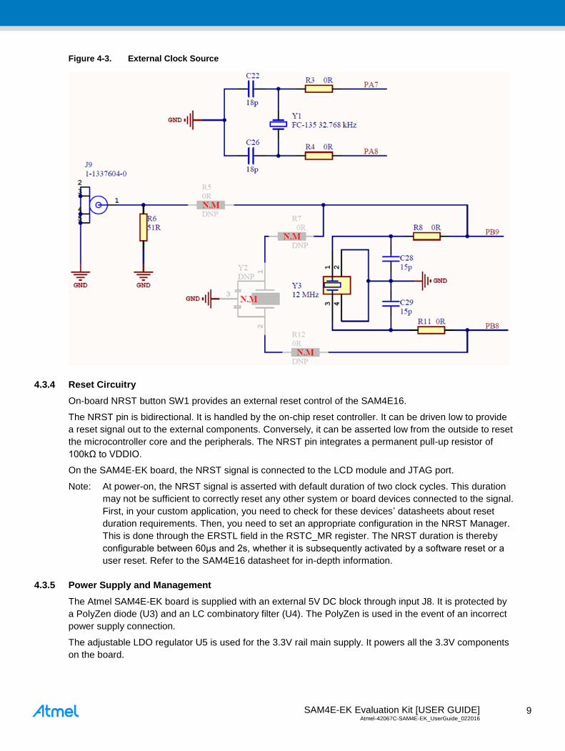
4.3.5 Power Supply and Management
The Atmel SAM4E-EK board is supplied with an external 5V DC block through input J8. It is protected by
a PolyZen diode (U3) and an LC combinatory filter (U4). The PolyZen is used in the event of an incorrect
power supply connection.
The adjustable LDO regulator U5 is used for the 3.3V rail main supply. It powers all the 3.3V components
on the board.
SAM4E-EK Evaluation Kit [USER GUIDE] Atmel-42067C-SAM4E-EK_UserGuide_022016 1
0
10
Figure 4-4. Power Block
The SAM4E16 product has different types of power supply pins:
VDDIN pin:
Power for the internal voltage regulator, ADC, DAC, and analog comparator power supplies.
The voltage ranges from 1.6 to 3.6V.
VDDIO pins:
Power for the Peripherals I/O lines.
The voltage ranges from 1.62 to 3.6V.
VDDOUT pin:
Output of the internal voltage regulator.
VDDCORE pins:
Power for the core, including the processor, embedded memories, and peripherals.
The voltage ranges from 1.08 to 1.32V.
VDDPLL pin:
Power for the PLL A, PLL B and 12MHz oscillator.
The voltage ranges from 1.08 to 1.32V.
Note: VDDPLL should be decoupled and filtered from VDDCORE.
SAM4E-EK Evaluation Kit [USER GUIDE] Atmel-42067C-SAM4E-EK_UserGuide_022016
1
1
11
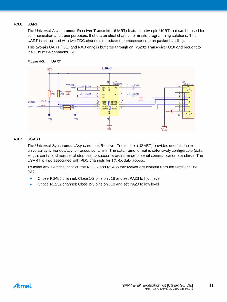
4.3.6 UART
The Universal Asynchronous Receiver Transmitter (UART) features a two-pin UART that can be used for
communication and trace purposes. It offers an ideal channel for in-situ programming solutions. This
UART is associated with two PDC channels to reduce the processor time on packet handling.
This two-pin UART (TXD and RXD only) is buffered through an RS232 Transceiver U10 and brought to
the DB9 male connector J20.
Figure 4-5. UART
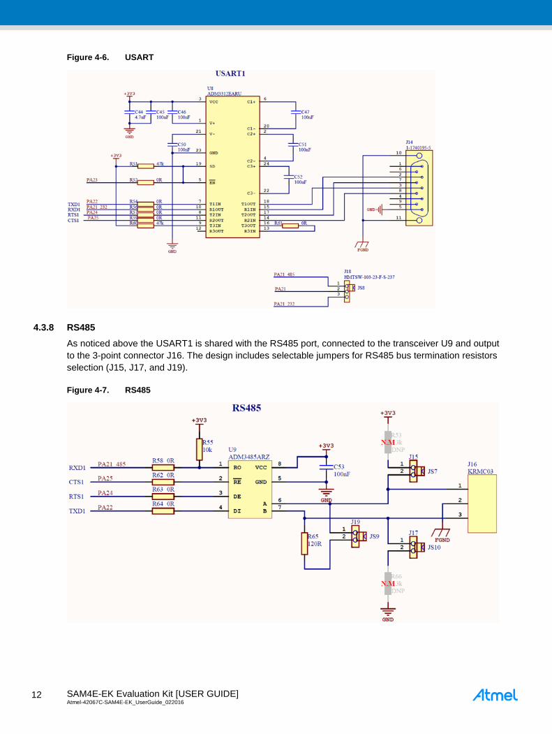
4.3.7 USART
The Universal Synchronous/Asynchronous Receiver Transmitter (USART) provides one full duplex
universal synchronous/asynchronous serial link. The data frame format is extensively configurable (data
length, parity, and number of stop bits) to support a broad range of serial communication standards. The
USART is also associated with PDC channels for TX/RX data access.
To avoid any electrical conflict, the RS232 and RS485 transceiver are isolated from the receiving line
PA21.
Chose RS485 channel: Close 1-2 pins on J18 and set PA23 to high level
Chose RS232 channel: Close 2-3 pins on J18 and set PA23 to low level
SAM4E-EK Evaluation Kit [USER GUIDE] Atmel-42067C-SAM4E-EK_UserGuide_022016 1
2
12
Figure 4-6. USART
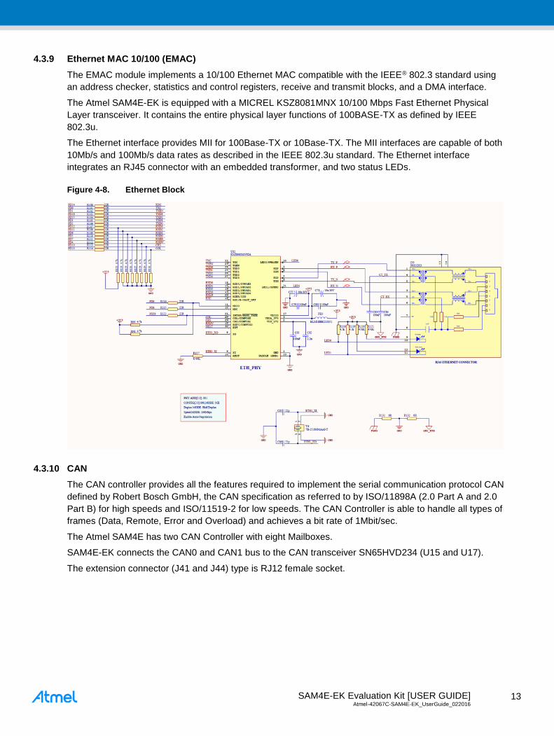
4.3.8 RS485
As noticed above the USART1 is shared with the RS485 port, connected to the transceiver U9 and output
to the 3-point connector J16. The design includes selectable jumpers for RS485 bus termination resistors
selection (J15, J17, and J19).
Figure 4-7. RS485
SAM4E-EK Evaluation Kit [USER GUIDE] Atmel-42067C-SAM4E-EK_UserGuide_022016
1
3
13
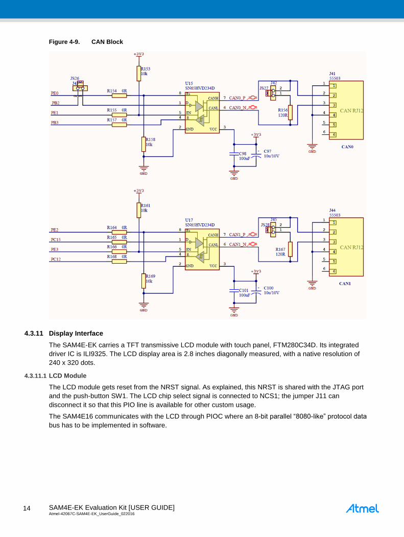
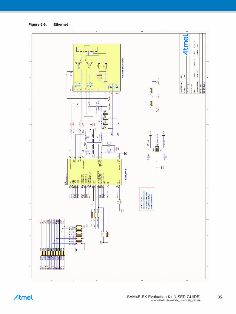
4.3.9 Ethernet MAC 10/100 (EMAC)
The EMAC module implements a 10/100 Ethernet MAC compatible with the IEEE® 802.3 standard using
an address checker, statistics and control registers, receive and transmit blocks, and a DMA interface.
The Atmel SAM4E-EK is equipped with a MICREL KSZ8081MNX 10/100 Mbps Fast Ethernet Physical
Layer transceiver. It contains the entire physical layer functions of 100BASE-TX as defined by IEEE
802.3u.
The Ethernet interface provides MII for 100Base-TX or 10Base-TX. The MII interfaces are capable of both
10Mb/s and 100Mb/s data rates as described in the IEEE 802.3u standard. The Ethernet interface
integrates an RJ45 connector with an embedded transformer, and two status LEDs.
Figure 4-8. Ethernet Block
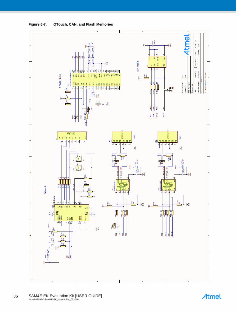
4.3.10 CAN
The CAN controller provides all the features required to implement the serial communication protocol CAN
defined by Robert Bosch GmbH, the CAN specification as referred to by ISO/11898A (2.0 Part A and 2.0
Part B) for high speeds and ISO/11519-2 for low speeds. The CAN Controller is able to handle all types of
frames (Data, Remote, Error and Overload) and achieves a bit rate of 1Mbit/sec.
The Atmel SAM4E has two CAN Controller with eight Mailboxes.
SAM4E-EK connects the CAN0 and CAN1 bus to the CAN transceiver SN65HVD234 (U15 and U17).
The extension connector (J41 and J44) type is RJ12 female socket.
SAM4E-EK Evaluation Kit [USER GUIDE] Atmel-42067C-SAM4E-EK_UserGuide_022016 1
4
14
Figure 4-9. CAN Block
4.3.11 Display Interface
The SAM4E-EK carries a TFT transmissive LCD module with touch panel, FTM280C34D. Its integrated
driver IC is ILI9325. The LCD display area is 2.8 inches diagonally measured, with a native resolution of
240 x 320 dots.
4.3.11.1 LCD Module
The LCD module gets reset from the NRST signal. As explained, this NRST is shared with the JTAG port
and the push-button SW1. The LCD chip select signal is connected to NCS1; the jumper J11 can
disconnect it so that this PIO line is available for other custom usage.
The SAM4E16 communicates with the LCD through PIOC where an 8-bit parallel “8080-like” protocol data
bus has to be implemented in software.
SAM4E-EK Evaluation Kit [USER GUIDE] Atmel-42067C-SAM4E-EK_UserGuide_022016
1
5
15
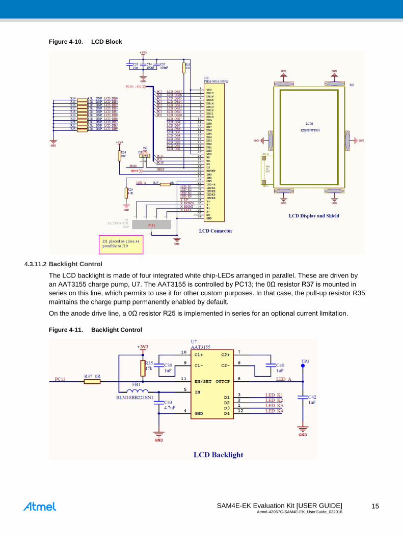
Figure 4-10. LCD Block
4.3.11.2 Backlight Control
The LCD backlight is made of four integrated white chip-LEDs arranged in parallel. These are driven by
an AAT3155 charge pump, U7. The AAT3155 is controlled by PC13; the 0Ω resistor R37 is mounted in
series on this line, which permits to use it for other custom purposes. In that case, the pull-up resistor R35
maintains the charge pump permanently enabled by default.
On the anode drive line, a 0Ω resistor R25 is implemented in series for an optional current limitation.
Figure 4-11. Backlight Control
SAM4E-EK Evaluation Kit [USER GUIDE] Atmel-42067C-SAM4E-EK_UserGuide_022016 1
6
16
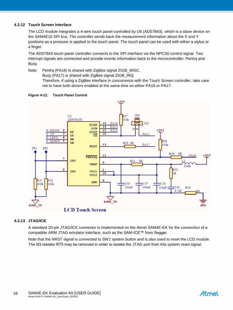
4.3.12 Touch Screen Interface
The LCD module integrates a 4-wire touch panel controlled by U6 (ADS7843), which is a slave device on
the SAM4E16 SPI bus. The controller sends back the measurement information about the X and Y
positions as a pressure is applied to the touch panel. The touch panel can be used with either a stylus or
a finger.
The ADS7843 touch panel controller connects to the SPI interface via the NPCS0 control signal. Two
interrupt signals are connected and provide events information back to the microcontroller: PenIrq and
Busy.
Note: PenIrq (PA16) is shared with ZigBee signal ZIGB_MISC.
Busy (PA17) is shared with ZigBee signal ZIGB_IRQ.
Therefore, if using a ZigBee interface in concurrence with the Touch Screen controller, take care
not to have both drivers enabled at the same time on either PA16 or PA17.
Figure 4-12. Touch Panel Control
4.3.13 JTAG/ICE
A standard 20-pin JTAG/ICE connector is implemented on the Atmel SAM4E-EK for the connection of a
compatible ARM JTAG emulator interface, such as the SAM-ICE™ from Segger.
Note that the NRST signal is connected to SW1 system button and is also used to reset the LCD module.
The 0Ω resistor R75 may be removed in order to isolate the JTAG port from this system reset signal.
SAM4E-EK Evaluation Kit [USER GUIDE] Atmel-42067C-SAM4E-EK_UserGuide_022016
1
7
17
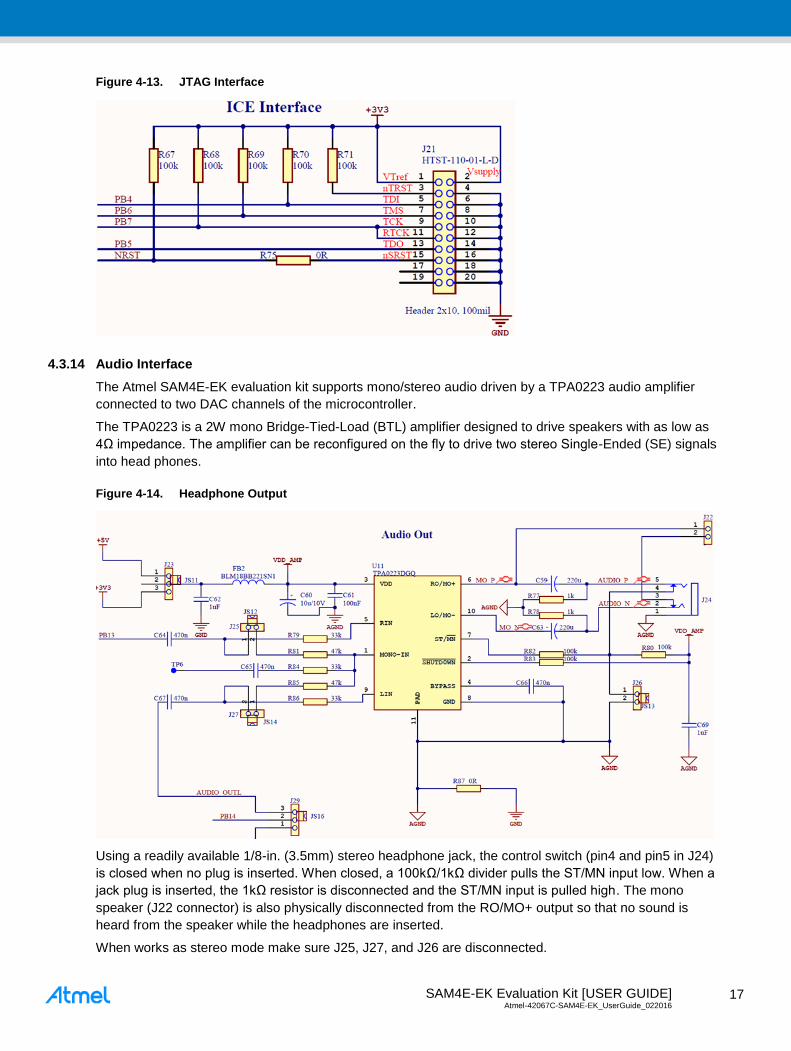
Figure 4-13. JTAG Interface
4.3.14 Audio Interface
The Atmel SAM4E-EK evaluation kit supports mono/stereo audio driven by a TPA0223 audio amplifier
connected to two DAC channels of the microcontroller.
The TPA0223 is a 2W mono Bridge-Tied-Load (BTL) amplifier designed to drive speakers with as low as
4Ω impedance. The amplifier can be reconfigured on the fly to drive two stereo Single-Ended (SE) signals
into head phones.
Figure 4-14. Headphone Output
Using a readily available 1/8-in. (3.5mm) stereo headphone jack, the control switch (pin4 and pin5 in J24)
is closed when no plug is inserted. When closed, a 100kΩ/1kΩ divider pulls the ST/MN input low. When a
jack plug is inserted, the 1kΩ resistor is disconnected and the ST/MN input is pulled high. The mono
speaker (J22 connector) is also physically disconnected from the RO/MO+ output so that no sound is
heard from the speaker while the headphones are inserted.
When works as stereo mode make sure J25, J27, and J26 are disconnected.
SAM4E-EK Evaluation Kit [USER GUIDE] Atmel-42067C-SAM4E-EK_UserGuide_022016 1
8
18
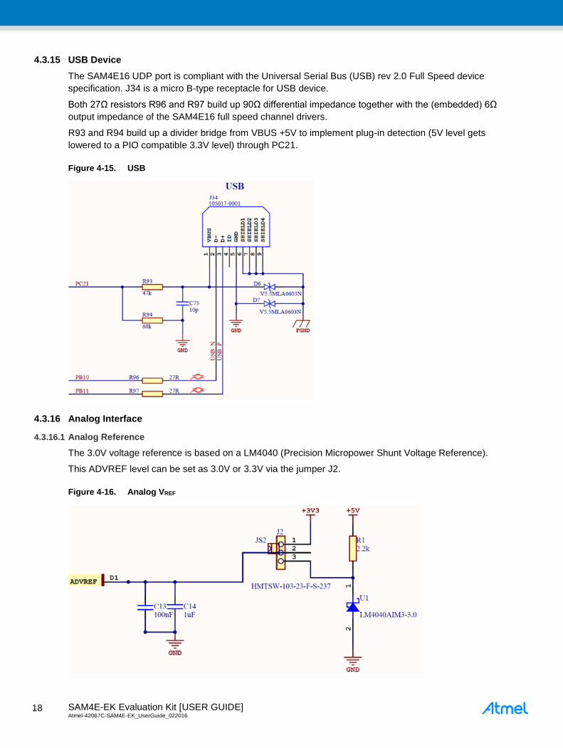
4.3.15 USB Device
The SAM4E16 UDP port is compliant with the Universal Serial Bus (USB) rev 2.0 Full Speed device
specification. J34 is a micro B-type receptacle for USB device.
Both 27Ω resistors R96 and R97 build up 90Ω differential impedance together with the (embedded) 6Ω
output impedance of the SAM4E16 full speed channel drivers.
R93 and R94 build up a divider bridge from VBUS +5V to implement plug-in detection (5V level gets
lowered to a PIO compatible 3.3V level) through PC21.
Figure 4-15. USB
4.3.16 Analog Interface
4.3.16.1 Analog Reference
The 3.0V voltage reference is based on a LM4040 (Precision Micropower Shunt Voltage Reference).
This ADVREF level can be set as 3.0V or 3.3V via the jumper J2.
Figure 4-16. Analog VREF
SAM4E-EK Evaluation Kit [USER GUIDE] Atmel-42067C-SAM4E-EK_UserGuide_022016
1
9
19
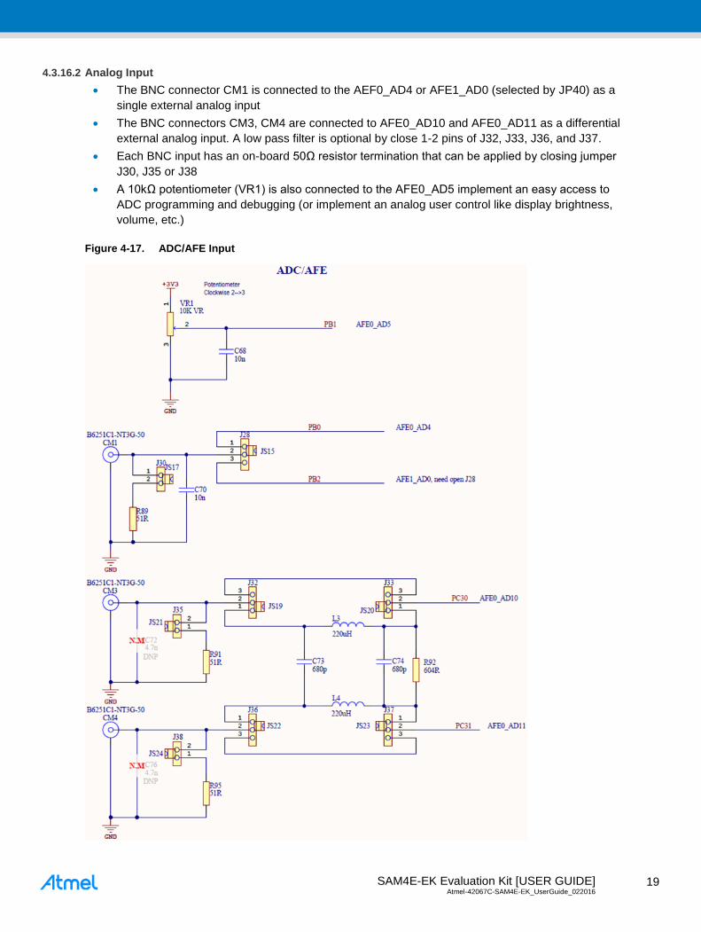
4.3.16.2 Analog Input
The BNC connector CM1 is connected to the AEF0_AD4 or AFE1_AD0 (selected by JP40) as a
single external analog input
The BNC connectors CM3, CM4 are connected to AFE0_AD10 and AFE0_AD11 as a differential
external analog input. A low pass filter is optional by close 1-2 pins of J32, J33, J36, and J37.
Each BNC input has an on-board 50Ω resistor termination that can be applied by closing jumper
J30, J35 or J38
A 10kΩ potentiometer (VR1) is also connected to the AFE0_AD5 implement an easy access to
ADC programming and debugging (or implement an analog user control like display brightness,
volume, etc.)
Figure 4-17. ADC/AFE Input
SAM4E-EK Evaluation Kit [USER GUIDE] Atmel-42067C-SAM4E-EK_UserGuide_022016 2
0
20
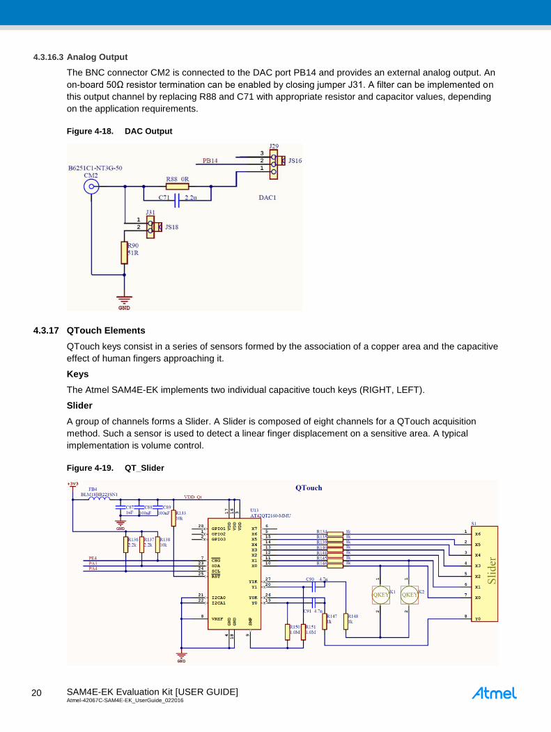
4.3.16.3 Analog Output
The BNC connector CM2 is connected to the DAC port PB14 and provides an external analog output. An
on-board 50Ω resistor termination can be enabled by closing jumper J31. A filter can be implemented on
this output channel by replacing R88 and C71 with appropriate resistor and capacitor values, depending
on the application requirements.
Figure 4-18. DAC Output
4.3.17 QTouch Elements
QTouch keys consist in a series of sensors formed by the association of a copper area and the capacitive
effect of human fingers approaching it.
Keys
The Atmel SAM4E-EK implements two individual capacitive touch keys (RIGHT, LEFT).
Slider
A group of channels forms a Slider. A Slider is composed of eight channels for a QTouch acquisition
method. Such a sensor is used to detect a linear finger displacement on a sensitive area. A typical
implementation is volume control.
Figure 4-19. QT_Slider
SAM4E-EK Evaluation Kit [USER GUIDE] Atmel-42067C-SAM4E-EK_UserGuide_022016
2
1
21
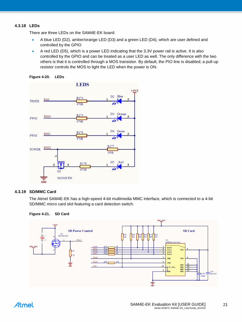
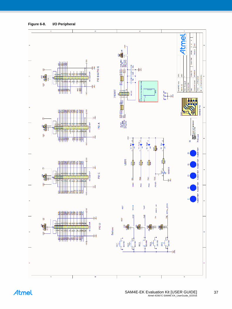
4.3.18 LEDs
There are three LEDs on the SAM4E-EK board:
A blue LED (D2), amber/orange LED (D3) and a green LED (D4), which are user defined and
controlled by the GPIO
A red LED (D5), which is a power LED indicating that the 3.3V power rail is active. It is also
controlled by the GPIO and can be treated as a user LED as well. The only difference with the two
others is that it is controlled through a MOS transistor. By default, the PIO line is disabled; a pull-up
resistor controls the MOS to light the LED when the power is ON.
Figure 4-20. LEDs
4.3.19 SD/MMC Card
The Atmel SAM4E-EK has a high-speed 4-bit multimedia MMC interface, which is connected to a 4-bit
SD/MMC micro card slot featuring a card detection switch.
Figure 4-21. SD Card
SAM4E-EK Evaluation Kit [USER GUIDE] Atmel-42067C-SAM4E-EK_UserGuide_022016 2
2
22
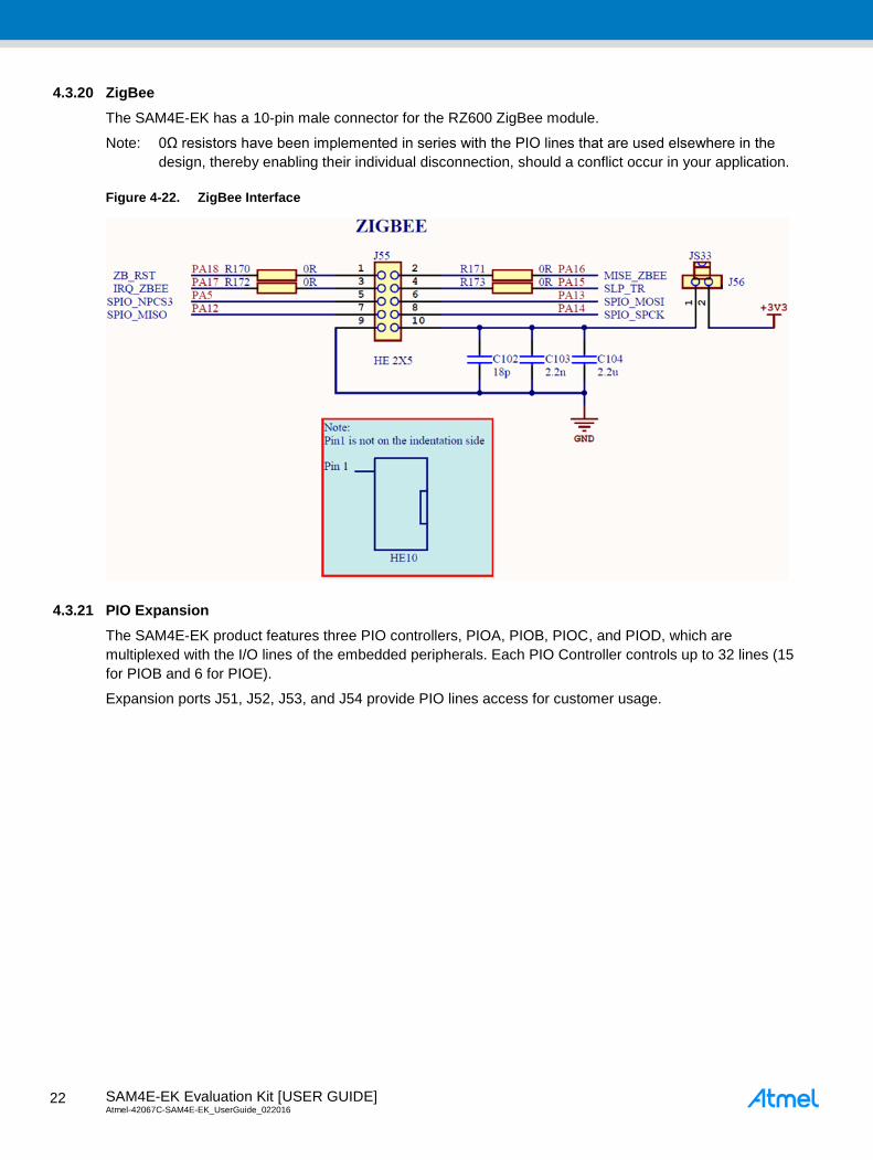
4.3.20 ZigBee
The SAM4E-EK has a 10-pin male connector for the RZ600 ZigBee module.
Note: 0Ω resistors have been implemented in series with the PIO lines that are used elsewhere in the
design, thereby enabling their individual disconnection, should a conflict occur in your application.
Figure 4-22. ZigBee Interface
4.3.21 PIO Expansion
The SAM4E-EK product features three PIO controllers, PIOA, PIOB, PIOC, and PIOD, which are
multiplexed with the I/O lines of the embedded peripherals. Each PIO Controller controls up to 32 lines (15
for PIOB and 6 for PIOE).
Expansion ports J51, J52, J53, and J54 provide PIO lines access for customer usage.
SAM4E-EK Evaluation Kit [USER GUIDE] Atmel-42067C-SAM4E-EK_UserGuide_022016
2
3
23
Figure 4-23. PIO Expansion
SAM4E-EK Evaluation Kit [USER GUIDE] Atmel-42067C-SAM4E-EK_UserGuide_022016 2
4
24
5 Configuration
This chapter describes the PIO usage, the jumpers, the test points and the solder drops of an Atmel
SAM4E-EK board.
5.1 PIO Usage
Table 5-1. PIO Port A Pin Assignments and Signal Descriptions
I/O line Peripheral A Peripheral B Peripheral C Extra function SYSIO and GPIO Comments
PA0 PWMH0 TIOA0 A17 WKUP0 LED_TIMER (Blue)
PA1 PWMH1 TIOB0 A18 WKUP1 BUTTON_SCROLL-UP
PA2 PWMH2 DATRG WKUP2 BUTTON_SCROLL-DOWN
PA3 TWD0 NPCS3 QTouch_SDA
PA4 TWCK0 TCLK0 WKUP3 QTouch_SCL
PA5 NPCS3 URXD1 WKUP4 ZIGB_SEL#, SPI FLASH_CS#
PA6 PCK0 UTXD1 SD_CD
PA7 PWMH3 XIN32 XIN32
PA8 AFE0_ADTRG WKUP5 XOUT32 XOUT32
PA9 URXD0 NPCS1 PWMFI0 WKUP6 DBGU_ROUT
PA10 UTXD0 NPCS2 DBGU_TIN
PA11 NPCS0 PWMH0 WKUP7 TOUCH_CS#
PA12 MISO PWMH1 TOUCH_DOUT, ZIGB_MISO,
SPI FLASH_SO
PA13 MOSI PWMH2 TOUCH_DIN, ZIGB_MOSI,
SPI FLASH_SI
PA14 SPCK PWMH3 WKUP8 TOUCH_DCLK, ZIGB_SCLK,
SPI FLASH_SCK
PA15 TIOA1 PWML3 WKUP14/PIODCEN1 ZIGB_SLP_TR
PA16 TIOB1 PWML2 WKUP15/PIODCEN2 TOUCH_PENIRQ#, ZIGB_MISC
PA17 PCK1 PWMH3 AFE0_AD0 TOUCH_BUZY, ZIGB_IRQ
PA18 PCK2 A14 AFE0_AD1 ZIGB_RST#
PA19 PWML0 A15 AFE0_AD2/WKUP9 BUTTON_WAKU
PA20 PWML1 A16 AFE0_AD3/WKUP10 BUTTON_TAMP
PA21 RXD1 PCK1 AFE1_AD2 RS232_RXD, RS485_RXD
PA22 TXD1 NPCS3 NCS2 AFE1_AD3 RS232_TXD, RS485_TXD
PA23 SCK1 PWMH0 A19 PIODCCLK RS232_EN#
PA24 RTS1 PWMH1 A20 PIODC0 RS232_RTS, RS485_DE
PA25 CTS1 PWMH2 A23 PIODC1 RS232_CTS, RS485_RE#
PA26 DCD1 TIOA2 MCDA2 PIODC2 SD_DAT2
PA27 DTR1 TIOB2 MCDA3 PIODC3 SD_DAT3
PA28 DSR1 TCLK1 MCCDA PIODC4 SD_CMD
PA29 RI1 TCLK2 MCCK PIODC5 SD_CLK
PA30 PWML2 NPCS2 MCDA0 WKUP11/PIODC6 SD_DAT0
PA31 NPCS1 PCK2 MCDA1 PIODC7 SD_DAT1
SAM4E-EK Evaluation Kit [USER GUIDE] Atmel-42067C-SAM4E-EK_UserGuide_022016
2
5
25
Table 5-2. PIO Port B Pin Assignments and Signal Descriptions
I/O line Peripheral A Peripheral B Peripheral C Extra function SYSIO and GPIO Comments
PB0 PWMH0 RXD0 AFE0_AD4/RTCOUT0 AFE0_BNC
PB1 PWMH1 TXD0 AFE0_AD5/RTCOUT1 ADC_Potentiometer
PB2 CANTX0 NCPS2 CTS0 AFE1_AD0/WKUP12 CAN0_D, AFE1_BNC
PB3 CANRX0 PCK2 RTS0 AFE1_AD1 CAN0_R
PB4 TWD1 PWMH2 TDI JTAG_TDI
PB5 TWCK1 PWML0 WKUP13 TDO/TRACESWO JTAG_TDO
PB6 TMS/SWDIO JTAG_TMS
PB7 TCK/SWCLK JTAG_TCK
PB8 XOUT XOUT
PB9 XIN XIN
PB10 DDP USB_D+
PB11 DDM USB_D-
PB12 PWML1 ERASE ERASE
PB13 PWML2 PCK0 SCK0 DAC0 AUDIO_RIN
PB14 NPCS1 PWMH3 DAC1 AUDIO_LIN, DAC1_BNC
Table 5-3. PIO Port C Pin Assignments and Signal Descriptions
I/O line Peripheral A Peripheral B Peripheral C Peripheral D Extra function SYSIO and GPIO Comments
PC0 D0 PWML0 AFE0_AD14 NAND_D0/LCD_DB10
PC1 D1 PWML1 AFE1_AD4 NAND_D1/LCD_DB11
PC2 D2 PWML2 AFE1_AD5 NAND_D2/LCD_DB12
PC3 D3 PWML3 AFE1_AD6 NAND_D3/LCD_DB13
PC4 D4 NPCS1 AFE1_AD7 NAND_D4/LCD_DB14
PC5 D5 TIOA6 NAND_D5/LCD_DB15
PC6 D6 TIOB6 NAND_D6/LCD_DB16
PC7 D7 TCLK6 NAND_D7/LCD_DB17
PC8 NWE TIOA7 LCD_WR
PC9 NANDOE TIOB7 NAND_OE#
PC10 NANDWE TCLK7 NAND_WE#
PC11 NRD TIOA8 LCD_RD
PC12 NCS3 TIOB8 CANRX1 AFE0_AD8 CAN1_R
PC13 NWAIT PWML0 AFE0_AD6 LCDBL_EN/SET
PC14 NCS0 TCLK8 NAND_CE#
PC15 NCS1 PWML1 CANTX1 AFE0_AD7 CAN1_D
PC16 A21/NANDALE NAND_ALE
PC17 A22/NANDCLE NAND_CLE
PC18 A0 PWMH0 NAND_R/B#
PC19 A1 PWMH1 LCD_RS
SAM4E-EK Evaluation Kit [USER GUIDE] Atmel-42067C-SAM4E-EK_UserGuide_022016 2
6
26
PC20 A2 PWMH2
PC21 A3 PWMH3 USB_VBUS
PC22 A4 PWML3
PC23 A5 TIOA3
PC24 A6 TIOB3
PC25 A7 TCLK3
PC26 A8 TIOA4 AFE0_AD12
PC27 A9 TIOB4 AFE0_AD13
PC28 A10 TCLK4
PC29 A11 TIOA5 AFE0_AD9
PC30 A12 TIOB5 AFE0_AD10 AFE0_BNC
PC31 A13 TCLK5 AFE0_AD11 AFE0_BNC
Table 5-4. PIO Port D Pin Assignments and Signal Descriptions
I/O line Peripheral A Peripheral B Peripheral C Peripheral D Extra function SYSIO and GPIO Comments
PD0 GTXCK/GREF
CK
MII_TXCK
PD1 GTXEN MII_TXEN
PD2 GTX0 MII_TX0
PD3 GTX1 MII_TX1
PD4 GCRSDV/GRX
DV
MII_RXDV
PD5 GRX0 MII_RX0
PD6 GRX1 MII_RX1
PD7 GRXER MII_RXER
PD8 GMDC ETH_MDC
PD9 GMDIO ETH_MDIO
PD10 GCRS MII_CRS
PD11 GRX2 MII_RX2
PD12 GRX3 MII_RX3
PD13 GCOL MII_COL
PD14 GRXCK MII_RXCK
PD15 GTX2 MII_TX2
PD16 GTX3 MII_TX3
PD17 GTXER
PD18 NCS1 LCD_CS
PD19 NCS3
PD20 PWMH0 LED_PWM (Amber)
PD21 PWMH1 LED_PWM (Green)
PD22 PWMH2 LED_PWR (RED)
PD23 PWMH3 SD_PWR_CTL
SAM4E-EK Evaluation Kit [USER GUIDE] Atmel-42067C-SAM4E-EK_UserGuide_022016
2
7
27
PD24 PWML0
PD25 PWML1
PD26 PWML2
PD27 PWML3
PD28 ETH_INTR
PD29
PD30
PD31
Table 5-5. PIO Port E Pin Assignments and Signal Descriptions
I/O line Peripheral A Peripheral B Peripheral C Peripheral
D
Extra function SYSIO and GPIO Comments
PE0 CAN0_Rs
PE1 CAN0_EN
PE2 CAN1_Rs
PE3 CAN1_EN
PE4 QTouch_CHANGE#
5.2 Jumpers
The Atmel SAM4E-EK board jumpers are essentially used for two main purposes: functional selection or
current measurement. Details are given below.
Table 5-6. 2-pin Jumpers Setting
Name Signal Close Open
J46 SPI FLASH_CS (NPCS3) Connect (default) Disconnect
J40 NAND_CE# (NCS0) Connect (default) Disconnect
J4 VDDCORE Connect (default) Disconnect
J1 VDDIO Connect (default) Disconnect
J3 VDDIN Connect (default) Disconnect
J43 CANTX0 CANTX0 can use AFE1_AD0 can use
J7 ERASE Erase internal flash Default
J12 TOUCH_CS# (NPCS0) Connect (default) Disconnect
J11 LCD_CS (NCS1) Connect (default) Disconnect
J59 BUTTON_SCROLL-UP Connect (default) Disconnect
J60 BUTTON_SCROLL-DOWN Connect (default) Disconnect
J58 BUTTON_TAMP Connect (default) Disconnect
J57 BUTTON_WAKU Connect (default) Disconnect
J25 PB13(DAC) to MONO-IN (Audio) Connect (default) Disconnect (default)
J27 PB14(DAC) to MONO-IN (Audio) Connect (default) Disconnect (default)
SAM4E-EK Evaluation Kit [USER GUIDE] Atmel-42067C-SAM4E-EK_UserGuide_022016 2
8
28
J26 Audio_ST/MN# Force mono mode No force (default)
J30, J31, J35 BNC input 50Ω match resister Use No use (default)
Name Signal 1-2 close 2-3 close
J18 PA21 RS485-RX RS232-RX
J2 ADVREF 3.3V (default) 3.0V
J23 Audio power 5V (default) 3.3V
J29 DAC_PB14 To CN1 (BNC) To Audio_LIN (default)
J47, J48, J49, J50 PIOA/B/C/D-CONN-power 5V 3.3V
J32, J33, J36, J37 AFE0_AD10/AD11 Use filter(default) Bypass filter
J28 ADC BNC input To AFE0_AD4 To AFE1_AD0
SAM4E-EK Evaluation Kit [USER GUIDE] Atmel-42067C-SAM4E-EK_UserGuide_022016
2
9
29
6 Schematics
This chapter contains the following schematics:
Block diagram
Microcontroller
TFT-LCD and touch
COM and SD card and JTAG
Audio and USB
Ethernet
QTouch, CAN, and Flash memories
I/O Peripheral
SAM4E-EK Evaluation Kit [USER GUIDE] Atmel-42067C-SAM4E-EK_UserGuide_022016 3
0
30
Figure 6-1. Block Diagram
SAM4E-EK Evaluation Kit [USER GUIDE] Atmel-42067C-SAM4E-EK_UserGuide_022016
3
1
31
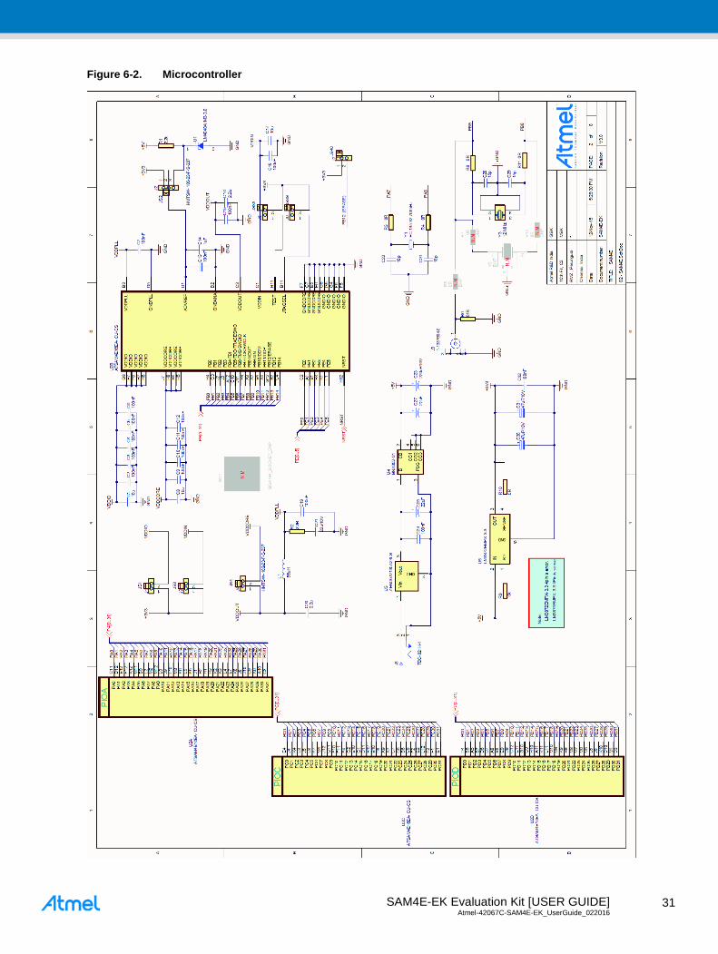
Figure 6-2. Microcontroller
SAM4E-EK Evaluation Kit [USER GUIDE] Atmel-42067C-SAM4E-EK_UserGuide_022016 3
2
32
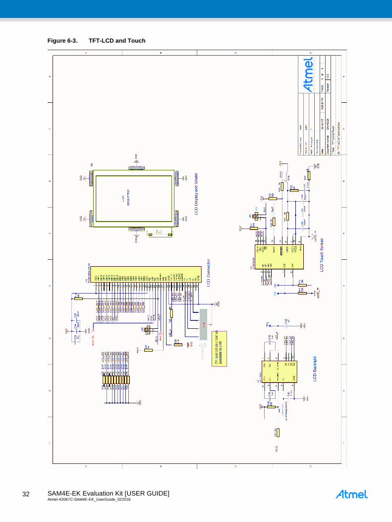
Figure 6-3. TFT-LCD and Touch
SAM4E-EK Evaluation Kit [USER GUIDE] Atmel-42067C-SAM4E-EK_UserGuide_022016
3
3
33
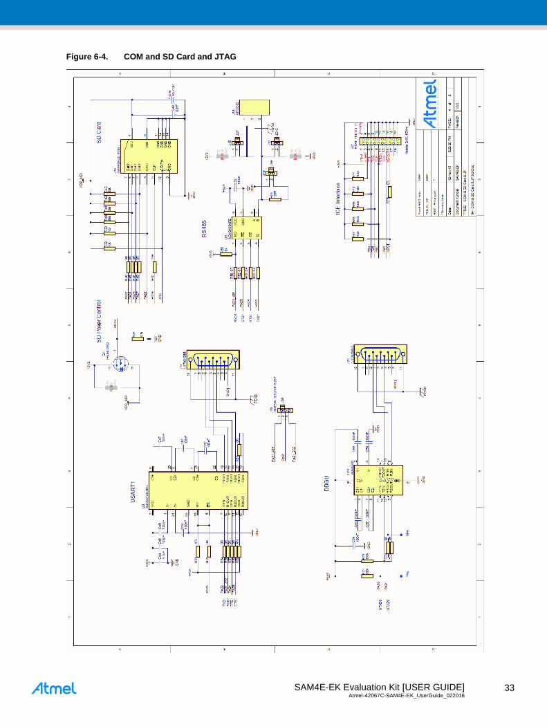
Figure 6-4. COM and SD Card and JTAG
SAM4E-EK Evaluation Kit [USER GUIDE] Atmel-42067C-SAM4E-EK_UserGuide_022016 3
4
34
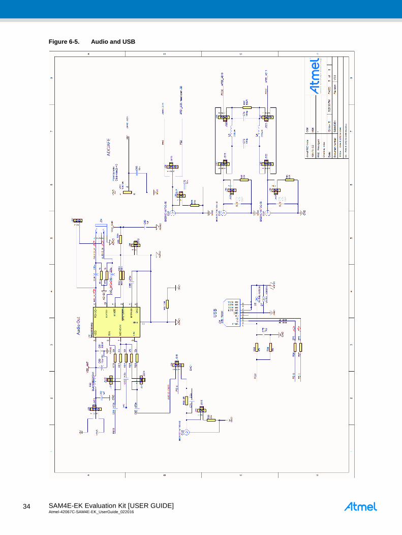
Figure 6-5. Audio and USB
SAM4E-EK Evaluation Kit [USER GUIDE] Atmel-42067C-SAM4E-EK_UserGuide_022016
3
5
35
Figure 6-6. Ethernet
SAM4E-EK Evaluation Kit [USER GUIDE] Atmel-42067C-SAM4E-EK_UserGuide_022016 3
6
36
Figure 6-7. QTouch, CAN, and Flash Memories
SAM4E-EK Evaluation Kit [USER GUIDE] Atmel-42067C-SAM4E-EK_UserGuide_022016
3
7
37
Figure 6-8. I/O Peripheral
SAM4E-EK Evaluation Kit [USER GUIDE] Atmel-42067C-SAM4E-EK_UserGuide_022016 3
8
38
7 ATMEL EVALUATION BOARD/KIT IMPORTANT NOTICE AND
DISCLAIMER
This evaluation board/kit is intended for user's internal development and evaluation purposes only. It is
not a finished product and may not comply with technical or legal requirements that are applicable to
finished products, including, without limitation, directives or regulations relating to electromagnetic
compatibility, recycling (WEEE), FCC, CE or UL. Atmel is providing this evaluation board/kit “AS IS”
without any warranties or indemnities. The user assumes all responsibility and liability for handling and
use of the evaluation board/kit including, without limitation, the responsibility to take any and all
appropriate precautions with regard to electrostatic discharge and other technical issues. User indemnifies
Atmel from any claim arising from user's handling or use of this evaluation board/kit. Except for the limited
purpose of internal development and evaluation as specified above, no license, express or implied, by
estoppel or otherwise, to any Atmel intellectual property right is granted hereunder. ATMEL SHALL NOT
BE LIABLE FOR ANY INDIRECT, SPECIAL, INCIDENTAL, OR CONSEQUENTIAL DAMGES RELATING
TO USE OF THIS EVALUATION BOARD/KIT.
ATMEL CORPORATION
1600 Technology Drive
San Jose, CA 95110
USA
SAM4E-EK Evaluation Kit [USER GUIDE] Atmel-42067C-SAM4E-EK_UserGuide_022016
3
9
39
8 Revision History
Doc Rev. Date Comments
42067C 02/2016 Updated to incorporate the changes latest revision of the kit.
Some minor changes according to the template.
42067B 04/2013 A feature is added to the feature list in Chapter 0.
Some typos are fixed.
42067A 01/2013 Initial document release.
SAM4E-EK Evaluation Kit [USER GUIDE] Atmel-42067C-SAM4E-EK_UserGuide_022016 4
0
40
Atmel Corporation 1600 Technology Drive, San Jose, CA 95110 USA T: (+1)(408) 441.0311 F: (+1)(408) 436.4200 www.atmel.com
© 2016 Atmel Corporation. / Rev.: Atmel-42067C-SAM4E-EK_UserGuide_022016. Atmel®, Atmel logo and combinations thereof, Enabling Unlimited Possibilities®, QTouch®, and others are registered trademarks or trademarks of Atmel Corporation in U.S. and other countries. ARM®, ARM Connected® logo, and others are the registered trademarks or trademarks of ARM Ltd. Other terms and product names may be trademarks of others. DISCLAIMER: The information in this document is provided in connection with Atmel products. No license, express or implied, b y estoppel or otherwise, to any intellectual property right is granted by this document or in connection with the sale of Atmel products. EXCEPT AS SET FORTH IN THE ATMEL TERMS AND COND ITIONS OF SALES LOCATED ON THE ATMEL WEBSITE, ATMEL ASSUMES NO LIABILITY WHATSOEVER AND DISCLAIMS ANY EXPRESS, IMPLIED OR STATUTORY WARRANTY RELATING TO ITS PRODUCTS
INCLUDING, BUT NOT LIMITED TO, THE IMPLIED WARRANTY OF MERCHANTABILITY, FITNESS FOR A PARTICULAR PURPOSE, OR NON -INFRINGEMENT. IN NO EVENT SHALL ATMEL BE LIABLE FOR ANY DIRECT, INDIRECT, CONSEQUENTIAL, PUNITIVE, SPECIAL OR INCIDENTAL DAMAGES (INCLUDING, WITHOUT LIMITATION, DAMAGES FOR LOSS AND PROFITS, BUSINESS INTERRUPTION, OR LOSS OF INFORMATION) ARISING OUT OF THE USE OR INABILITY TO USE THIS DOCUMENT , EVEN IF ATMEL
HAS BEEN ADVISED OF THE POSSIBILITY OF SUCH DAMAGES. Atmel makes no representations or warranties with respect to the accuracy or completeness of the conten ts of this document and reserves the right to make changes to specifications and products descriptions at any time without notice. Atmel does not make any commitment to update the information contained herein. Unless specifically provided otherwise, Atmel products are not suitable for, and shall not be used in, auto motive applications. Atmel products are not intended,
authorized, or warranted for use as components in applications intended to support or sustain life.
SAFETY-CRITICAL, MILITARY, AND AUTOMOTIVE APPLICATIONS DISCLAIMER: Atmel products are not designed for and will not be used in conne ction with any applications where the failure of such products would reasonably be expected to result in significant personal injury or death (“Safety -Critical Applications”) without an Atmel officer's specific written consent. Safety-Critical Applications include, without limitation, life support devices and systems, equipment or systems for the operation of nuclear facilities and weapons systems. Atmel
products are not designed nor intended for use in military or aerospace applications or environments unless specifically desi gnated by Atmel as military-grade. Atmel products are not
designed nor intended for use in automotive applications unless specifically designated by Atmel as automotive -grade.