Embed Size (px)
Citation preview
sakari tiuraniemi - CERN
Status of the submission – End of Column
sakari tiuraniemi - CERN
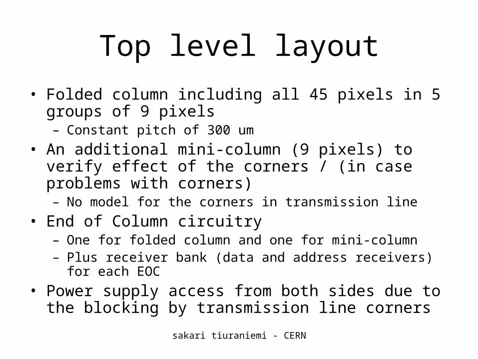
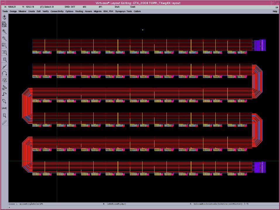
Top level layout
• Folded column including all 45 pixels in 5 groups of 9 pixels– Constant pitch of 300 um
• An additional mini-column (9 pixels) to verify effect of the corners / (in case problems with corners)– No model for the corners in transmission line
• End of Column circuitry – One for folded column and one for mini-column– Plus receiver bank (data and address receivers) for each EOC
• Power supply access from both sides due to the blocking by transmission line corners
sakari tiuraniemi - CERN
Top level layout
sakari tiuraniemi - CERN
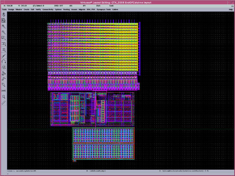
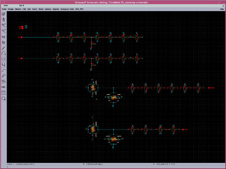
End of Column Layout
• TDC-bank of 9 TDC’s (18 hit registers) with differential to single-ended input buffer, DLL with differential buffer
• Missing in layout:– Start and stop trigger generation
• Designed on schematic level
– Shift register for serial data transmission• Designed on schematic level
– Coarse Counter• Designed on schematic level
– Address receivers and registers
sakari tiuraniemi - CERN
sakari tiuraniemi - CERN
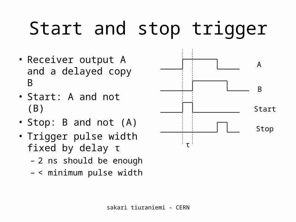
Start and stop trigger
• Receiver output A and a delayed copy B
• Start: A and not (B)• Stop: B and not (A)• Trigger pulse width
fixed by delay τ– 2 ns should be enough
– < minimum pulse width
A
B
Start
Stop
τ
sakari tiuraniemi - CERN
sakari tiuraniemi - CERN
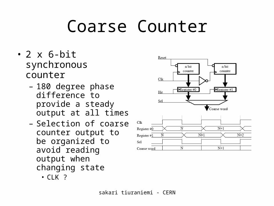
Coarse Counter
• 2 x 6-bit synchronous counter – 180 degree phase
difference to provide a steady output at all times
– Selection of coarse counter output to be organized to avoid reading output when changing state
• CLK ?
sakari tiuraniemi - CERN
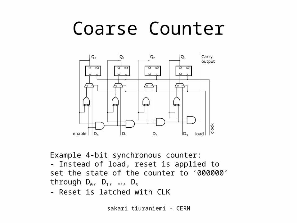
Coarse Counter
Example 4-bit synchronous counter:- Instead of load, reset is applied to set the state of the counter to ‘000000’ through D0, D1, …, D5
- Reset is latched with CLK

sakari tiuraniemi - CERN
Serial readout
• The data of each hit is stored in a shift register (parallel in, serial out - PISO)– Including rise and fall fine time (2 x 32 bits),
rise and fall coarse time (2 x 6 bits) and address (5 bits)
• all together 81 bits
• Serial data transmitted off chip by LVDS driver
• Ferrara readout as an alternative
sakari tiuraniemi - CERN
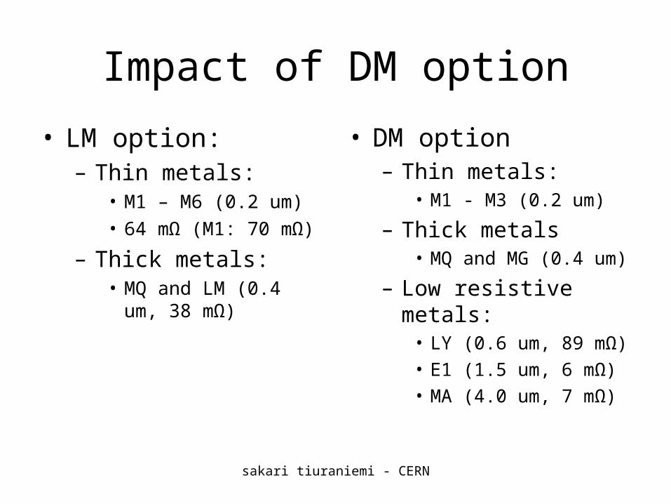
Impact of DM option
• LM option:– Thin metals:
• M1 – M6 (0.2 um)• 64 mΩ (M1: 70 mΩ)
– Thick metals:• MQ and LM (0.4 um, 38
mΩ)
• DM option– Thin metals:
• M1 - M3 (0.2 um)
– Thick metals• MQ and MG (0.4 um)
– Low resistive metals:• LY (0.6 um, 89 mΩ)• E1 (1.5 um, 6 mΩ)• MA (4.0 um, 7 mΩ)
sakari tiuraniemi - CERN
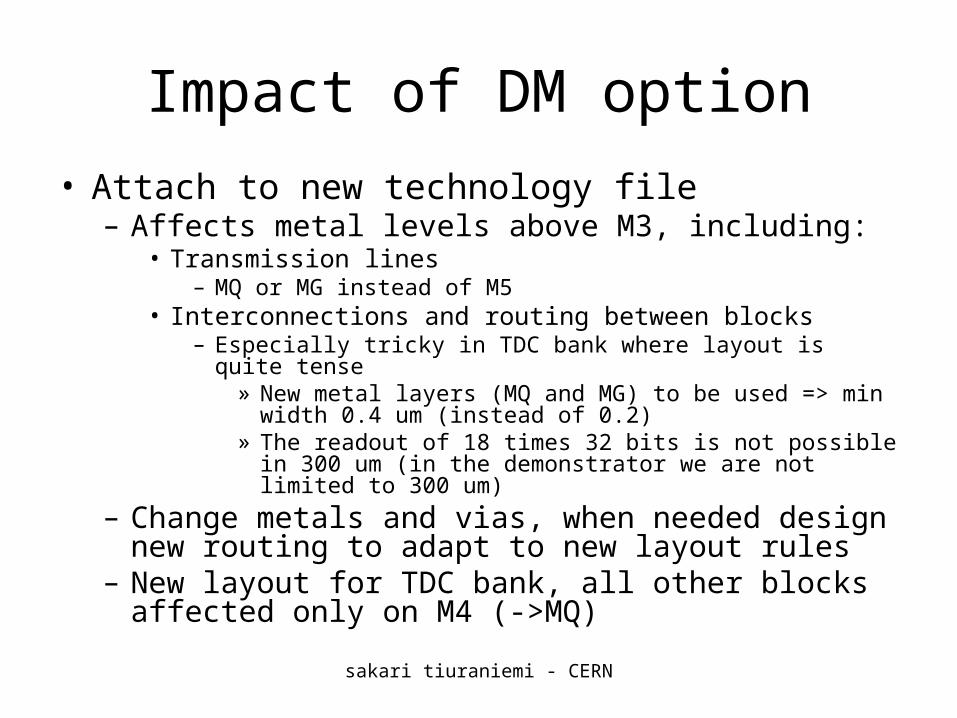
Impact of DM option
• Attach to new technology file– Affects metal levels above M3, including:
• Transmission lines– MQ or MG instead of M5
• Interconnections and routing between blocks– Especially tricky in TDC bank where layout is quite tense
» New metal layers (MQ and MG) to be used => min width 0.4 um (instead of 0.2)
» The readout of 18 times 32 bits is not possible in 300 um (in the demonstrator we are not limited to 300 um)
– Change metals and vias, when needed design new routing to adapt to new layout rules
– New layout for TDC bank, all other blocks affected only on M4 (->MQ)
sakari tiuraniemi - CERN
The End