Embed Size (px)
Citation preview

JOURNAL OF LIGHTWAVE TECHNOLOGY, VOL. 23, NO. 8, AUGUST 2005 2555
Sagnac Loop in Ring Resonatorsfor Tunable Optical Filters
Carmen Vázquez, Member, IEEE, Member, OSA, Salvador Elías Vargas,and José Manuel Sánchez Pena, Senior Member, IEEE
Abstract—General filter architecture using co- and counter-propagation signals are studied. A specific configuration based ona Sagnac loop within a ring resonator is analyzed. Novel tuning,apart from conventional tuning, is achieved by changing the cou-pling ratio of a coupler through the adjustment of the equivalentloop length. Full equations describing the filter behavior in passiveand active configurations, and simple closed-form formulas tocompute the tuning, tolerance, and full-width at half-maximumare reported. The performance of these devices is discussed fortheir application as selective or channel-dropping ultra-narrow-band filters. The effect of losses and their dispersion propertiesare also discussed. These devices can be conveniently implemented,using silicon- or InP-integrated optic technology, for they havehigh free spectral ranges.
Index Terms—Microresonators, optical filters, ring resonators,Sagnac loop, tuning and optical couplers.
I. INTRODUCTION
TUNABLE optical filters will be essential components infuture reconfigurable optical networks. They should have
ultra-narrow-bandwidth for use in dense-wavelength-divisionmultiplexing (DWDM) systems with carrier spacing of 50 GHzor less. On the other hand, the utilization of subcarrier-multiplexed (SCM) data channels in DWDM optical networkshas many potential important roles including packet addressing,performance monitoring using subcarriers, and network man-agement and control. These systems require an efficient methodto monitor, extract, and potentially erase subcarrier information.In this respect, optical filtering techniques have been used tosimplify SCM receiver designs [1]. These filters must have highrejection ratios and free spectral ranges (FSRs) in the order oftenths of gigahertz. Narrow-band optical filters are also usefulin photonic links that engage in high-speed optical RF signals.Another interesting approach is to have filter structures that canbe monolithically integrated in a chip.
Common filter technology available includes arrayed-waveguide gratings, thin-film dielectric interference filters,conventional fiber Bragg gratings (FBGs), fiber Fabry–Pérotfilters, and Mach–Zehnder (MZ) interferometers. A completereview, including most of these technologies, can be seen in[2]–[4]. However, these devices have difficulty providing either
Manuscript received October 14, 2004; revised April 5, 2005. This work wassupported by the Spanish Ministry of Education and Science CICYT (TIC2003-03783).
The authors are with the Electronic Technology Department, UniversityCarlos III of Madrid, 28911 Madrid, Spain (e-mail: [email protected]).
Digital Object Identifier 10.1109/JLT.2005.850793
notch or bandpass filters with ultranarrow bandwidths. Theserequirements can be covered by optical filters based on ringresonators (RRs) and loop mirrors [4]–[12]. These ring-basedfilters have been utilized in numerous linear and nonlinearoptical applications [10], including biochemical sensors [14]and all-optical switches [13]. Even various compound RRs[15]–[17] and discontinuity-assisted RRs [18], which are con-structed by an RR and a reflective section within it, are reportedand analyzed by different methods. However, these filters aretuned by varying the phase delay of the waveguides, and thereflective section is implemented either by a Fabry–Pérot cavity,by a grating, or by a waveguide with a different refractiveindex.
Tunable filters based on RR and a Michelson interferometer(MI) as the reflective element in the feedback path are reportedin [19], with the MI made of a directional coupler and twoidentical FBGs. But in this MI configuration, the fabricationtolerances impose a limit in the balance of the interferencepaths, and consequently, in the filter behavior. The use of aSagnac interferometer as the reflective element [20] alleviatesthis problem, because of its common-path architecture. Thisconfiguration is experimentally tested in its passive form in[21]. In any of these configurations, it is necessary to have avariable coupling coefficient, and its accuracy and tolerancesmust be analyzed. Tolerance effects on an RR with a FBG filterin transmission mode within it are reported in [7], where it wasalso proposed that it be controlled by using a variable loss orgain. Coupling coefficient tolerance effect, in terms of tuningcapabilities, has not yet been analyzed.
In this paper, we report a detailed study of the generalarchitecture of a tunable filter, based on an RR and a reflectivesection in the feedback path, working in its passive and activeforms, depending on the application. The filter response iscalculated using two different methods, the transfer matrixformalism and the z-transform technique, and the same ex-pressions are obtained independently. Losses are included inthe model. Simple equations are shown for helping the designprocess when using a specific reflective section, a Sagnac loop.The present analysis is restricted to couplers characterizedby two parameters, the power coupling coefficient, and thepower excess loss. Tuning is achieved by changing the phasedelay in the ring or Sagnac waveguides and additionally bychanging the coupling coefficient of the Sagnac loop. Simpleclosed-form formulas describing the novel tuning process arederived in its active and passive configurations, along withthe requirements for having a certain operation as a bandpass
0733-8724/$20.00 © 2005 IEEE

2556 JOURNAL OF LIGHTWAVE TECHNOLOGY, VOL. 23, NO. 8, AUGUST 2005
or bandstop filter. Measurements on a fiber-optic prototypevalidating the theoretical model, and the tunability, are reportedelsewhere [21]. Coupling coefficient tolerance effect, in termsof tuning capabilities, is also analyzed. These filters can beimplemented in optical fiber technology and in silicon- or InP-integrated optic technologies, because photonic circuits withequivalent components have already been developed. Some ofthem are a monolithically integrated Sagnac interferometer foran all-optical controlled-NOT gate [22], filters using active RRs[23], [24], passive single- and double-RRs [8], [25]–[27] andmicrocavities [28]. The resonant frequencies of the proposeddevice can be shifted by changing the equivalent loop length bycarrier injection [29] or local heating [30], as in any RR-baseddevice. The transfer function can be tailored by changing theloop loss; and if III–V materials are used in the fabrication,this can be done by electroabsorption [31]. The filter resonantfrequencies can also be changed by tuning the coupling ratio,which up to now is technologically possible by adjusting thetaper–resonator gap fabricated by stretching a standard opticalfiber [28]; by a micromechanical-fiber variable-ratio coupler,using microelectromechanical systems (MEMS) actuated de-formable waveguides [32], or by using electrical control ofwaveguide-resonator coupling in an MZ coupler configuration[33], [34]. Although present analysis is particularized to cou-plers characterized by two parameters, general equations canbe particularized to each technological solution.
The paper is focused on the presentation of the architecture,and it is structured as follows. Section II presents the generalarchitecture and its basic theoretical description, including thetransfer function for the different output ports. In Section III,a specific scheme using a Sagnac loop is described in its ac-tive and passive forms, and tuning equations are reported.Section IV elaborates on different filter applications, closed-form expressions for calculating some relevant design pa-rameters, coupling-ratio tolerances, and the filter dispersionproperties. Finally, Section V elaborates on the summary andconclusion.
II. FILTER ARCHITECTURE AND GENERAL EQUATIONS
In this section, we present the general architecture of theproposed filter, which consists of compound devices in a ringconfiguration with a reflective section. From a digital filter pointof view, they are infinite impulse response (IIR) filters whosepoles can be located radially using a gain or loss and axiallyusing a coupling coefficient K. For a filter made up of a singlestage, this property implies that tuning can be achieved through
the K value. The transfer function of the filter is derived usingtwo methods: the general matrix formalism, as in [16], and thez-transform technique [4].
The filter architecture is shown in Fig. 1. It is made up ofan RR, a transmission–reflection function (TRF), which repre-sents the reflective section, and different transmission functionsbefore and after the TRF. This TRF has a transfer function inreflection and in transmission named FR and FT, respectively.
A. General Equations Using the Matrix Formalism
The transfer-matrix method is used for calculating the trans-fer function of a compound device that is made of concatenatedelementary devices; and each of them can be represented byits own transfer matrix. In our filter, there are clockwise andcounterclockwise propagation, so the device is unfolded intotwo simple traveling-wave resonators connected by the TRF(Fig. 2), as reported in [16], where a compound-fiber RR is alsoanalyzed. Afterwards, the transmission matrix of the coupler,the waveguides, and the TRF will be used.
The transfer function of the filter can be straightforwardlyobtained by applying
[E1
E3
]= [ac][g][TRF][g′][ac′]
[E ′r
1
E ′3
](1)
where E′r1 is the reflected output at port E1, E ′
3 is the inputpower at port E3 (which in our analysis is equal to 0), while E1
is the input and E3 is the output (see Fig. 2). The expressionsof the matrices of (1) can be seen in Appendix A.
From the above expressions, it can be derived that the outputtransfer function at port E3 is given by (2), shown at the bottomof page, where K1 and γ1 are the coupling coefficient and theexcess loss of the input coupler, respectively. α and β are thewaveguide attenuation and the propagation constant, respec-tively, LT is the total waveguide length, and la is the waveguidelength connecting the input coupler and the TRF (seeFig. 1), ΠN
1 (Txi) and ΠM
1 (Tyi) are the N transmission trans-
fer functions between the input coupler and the TRF, and theM transmission transfer functions between the TRF and theinput coupler, respectively.
From (2), it is observed that the TRF position within the RRhas no importance, because there is no dependence on la. Butit is important in deriving the reflected output transfer functionat port E1, which is given by (3), shown at the bottom of thenext page.
E3
E1= (1−γ1)
12
×[
(1−K1)12 − (1−γ1)
12 (2−K1)(ΠTxi
)(ΠTyi)FTe−(α+jβ)LT(1−γ1)(1−K1)
12 (ΠTxi
)2(ΠTyi)2(FT2−FR2)e−2(α+jβ)LT
1−2(1−γ1)12 (1−K1)
12 (ΠTxi
)(ΠTyi)FTe−(α+jβ)LT(1−γ1)(1−K1)(ΠTxi
)2(ΠTyi)2(FT2−FR2)e−2(α+jβ)LT
]
(2)

VÁZQUEZ et al.: SAGNAC LOOP IN RING RESONATORS FOR TUNABLE OPTICAL FILTERS 2557
Fig. 1. General filter architecture. Txi and Tyi are any of the N and M transmission transfer functions placed before and after the TRF, and LT is the ring totallength. The inset is a schematic of a loop Sagnac as the TRF.
Both transfer functions [see (2) and (3)] have the same de-nominator, which can be factorized as
F1 × F2 =[1 − (1 − γ1)
12 (1 − K1)
12 (ΠTxi
) (ΠTyi)
× (FT + FR) e−(α+jβ)LT
]
×[1 − (1 − γ1)
12 (1 − K1)
12 (ΠTxi
) (ΠTyi)
× (FT − FR) e−(α+jβ)LT
]. (4)
There is only one difference in these two factors, the termrelated to FT and FR, in the first factor F1 they are added up,and in the second one F2 they are subtracted.
The λ values, which make any of these two factors 0, arethe resonance wavelengths. Selecting FT and FR in a waythat FR is an imaginary number and FT is a real number (or
Fig. 2. Unfolded equivalent model of the compound ring resonator.
vice versa), we can have phase dependence for controlling theresonance wavelengths location. A specific example is devel-oped in Section III.
E ′r1
E1=
− (1−γ1) K1 (ΠTxi)2 FRe−2(α+jβ)la
1−2 (1−γ1)12 (1−K1)
12 (ΠTxi
) (ΠTyi) FTe−(α+jβ)LT (1−γ1) (1−K1) (ΠTxi
)2 (ΠTyi)2
(FT2−FR2
)e−2(α+jβ)LT
.
(3)

2558 JOURNAL OF LIGHTWAVE TECHNOLOGY, VOL. 23, NO. 8, AUGUST 2005
B. General Equations Using the z-Transform Technique
Another approach for obtaining the compound-device trans-fer function has been used, the z-transform technique. Thisis commonly used in designing photonic filters from a digitalperspective [4]. A second-order polynomial in the denominatoris obtained, so transfer functions not available with a singleRR can be achieved. Our main purposes are to corroborate theexpressions derived in Section I-A and obtaining the pole andzero locations for synthesis purposes, which will be describedelsewhere.
In order to be able to correctly apply the z-transform tech-nique, the IIR of the device must have a unitary delay (τ). Thesignal that passes through the TRF travels a total length LT, andthe reflected signal at the TRF travels twice this total length, soτ = nefLT/c, where nef is the waveguide effective refractiveindex, and c is the light speed in a vacuum.
The following transfer functions at port E3 are obtained(see Appendix B):
E3
E1= (1 − γ1)
12 (1 − K1)
12
[1 + Bz−1 + Cz−2
(1 − Zp1z−1)(1 − Zp2z−1)
](5)
where Zp1 and Zp2 are the poles of the transfer function and aregiven by
Zp1 = (1−γ1)12 (1−K1)
12
N∏i=1
Txi
M∏i=1
Tyi[FT+FR] (6)
Zp2 = (1−γ1)12 (1−K1)
12
N∏i=1
Txi
M∏i=1
Tyi[FT−FR] (7)
where FR and FT are, respectively, the transfer function inreflection and in transmission of the TRF, and z−1 representsthe unit delay related to LT.
B and C are given by
B =(1 − γ1)
12 (K1 − 2)
N∏i=1
Txi·
M∏i=1
Tyi· FT
(1 − K1)12
(8)
C = (1 − γ1)N∏
i=1
Txi
M∏i=1
Tyi[FT2 − FR2]. (9)
This new representation of the transfer function can be usedto determine the value range of the device parameters fordesigning a stable filter. The modulus of the poles [from (6)and (7)] must be within the unit circle to avoid an infinitetransmission, i.e., laser oscillation.
The transfer function at port E3, given by (2) in Section II-A,and by (5) in this section, are equal, and the two factors of thedenominator given by (3) are the two poles described in (6)and (7). This is a way of verifying that all the expressions arecorrectly derived.
III. RING RESONATOR WITH A SAGNAC LOOP
In this section, a specific tunable filter design is proposed.The design includes an active RR, and the TRF in the RRis implemented by a Sagnac Loop. A schematic of the pro-posed filter is shown in Fig. 1, using the TRF described inthe inset. The amplifier, with a power gain G, amplifies theclockwise and the counterclockwise signals, so no isolators areconsidered.
The Sagnac interferometer has been used for extractingmodulated channels in a subcarrier in WDM networks [1], asa two-position switch with FBGs [35], with an active RR as alaser of two ultrafine lines [36], and with an RR as a birefrin-gence magnifier [37], apart from numerous sensor applications.
In this design, it is used as a mirror with variable reflectance,generating variable clockwise and counterclockwise signalsthat interfere with each other. In comparison with other alter-natives, such as an MI [19], it is easier to physically implementworking in a coherent regimen, because the two arms of theinterferometer are of the same fiber, making the alignmentstraightforward. In the case of two physically different arms,i.e., made of theoretically two identical FBGs, the tolerancein fabrication could alter the desired equal length betweenboth paths.
The Sagnac interferometer is a device having a TRF thatpartially transmits (FT) and reflects (FR), the input light. Thesefunctions are given by
FR = j2(1 − γ2)√
K2(1 − K2) (10)
FT = (1 − γ2)(1 − 2K2) (11)
where γ2 and K2 are the excess loss and the coupling coefficientof the coupler connecting the Sagnac loop, respectively (seeinset of Fig. 1). In (10) and (11), waveguide attenuation andretardation in signal propagation are not included, because bothhave already been considered in general in (2) and (3).
In the following, the frequencies at which transfer functionswill have a maximum or a minimum and any condition re-quired to effectively have them are going to be determined.A description of how these frequencies can be tuned is alsoreported.
A. Maximum Resonance Condition and Frequency Location
The maximum frequencies of the transfer function can be de-rived by requiring both the real and the imaginary componentsof the denominator of E3 to be equal to 0. This denominator,for the specific design with a Sagnac Loop, is obtained bysubstituting (10) and (11) in (3). The two factors F1 and F2
are written as
F1 =[1 − (1 − γ1)
12 (1 − K1)
12 G
12 (FT + FR)e−(α+jβ)LT
](12)
F2 =[1 − (1 − γ1)
12 (1 − K1)
12 G
12 (FT − FR)e−(α+jβ)LT
](13)
VÁZQUEZ et al.: SAGNAC LOOP IN RING RESONATORS FOR TUNABLE OPTICAL FILTERS 2559
where
FT + FR = (1 − γ2)ejφs (14)
FT − FR = (1 − γ2)e−jφs (15)
and
φs = ± arg
(2√
K2(1 − K2)(1 − 2K2)
). (16)
Both factors F1 and F2 are 0 if
G12 =
1(1 − γ1)
12 (1 − γ2)(1 − K1)
12 e−αLT
= Gp12 (17)
and
2πk =2πf1,2nef
cLT ∓ φs, k = 1, 2, 3, . . . (18)
where f1,2 is the frequency in hertz and the subscripts “1” and“2” refer to the factors F1 and F2, respectively.
Gp is a new parameter that we have defined, it is named polegain, and it represents the resonance condition of the maxima.
From (18), we obtain the FSR of the compound device as
FSR =c
nefLT. (19)
The maximum frequencies are derived from (18), and theamplitude of the transfer function at these frequencies (the res-onance peak) can be made arbitrarily narrow and sharp. WhenGp = 1, we obtain, according to (2), an infinite transmission,i.e., laser oscillation. Gp can be used as a parameter to controlthe peak resonance value.
B. Maximum Frequencies Tuning by Changingthe Coupling Coefficient
The poles of the transfer function are complex conjugatednumbers, which are obtained by substituting (14) and (15) into(6) and (7), and their phases depend not only on the opticalpath, but also on K2. This phase determines the maximumfrequency, which consequently, can be controlled through thecoupling coefficient. The same conclusion can be derived from(16) and (18). If we want to tune the filter maximum of order kto a specific frequency f0, we first obtain
k =f0
FSR. (20)
From (18) and (19), we obtain the maximum frequency as
f1,2 = f0 ±cφs
2πnefLT. (21)
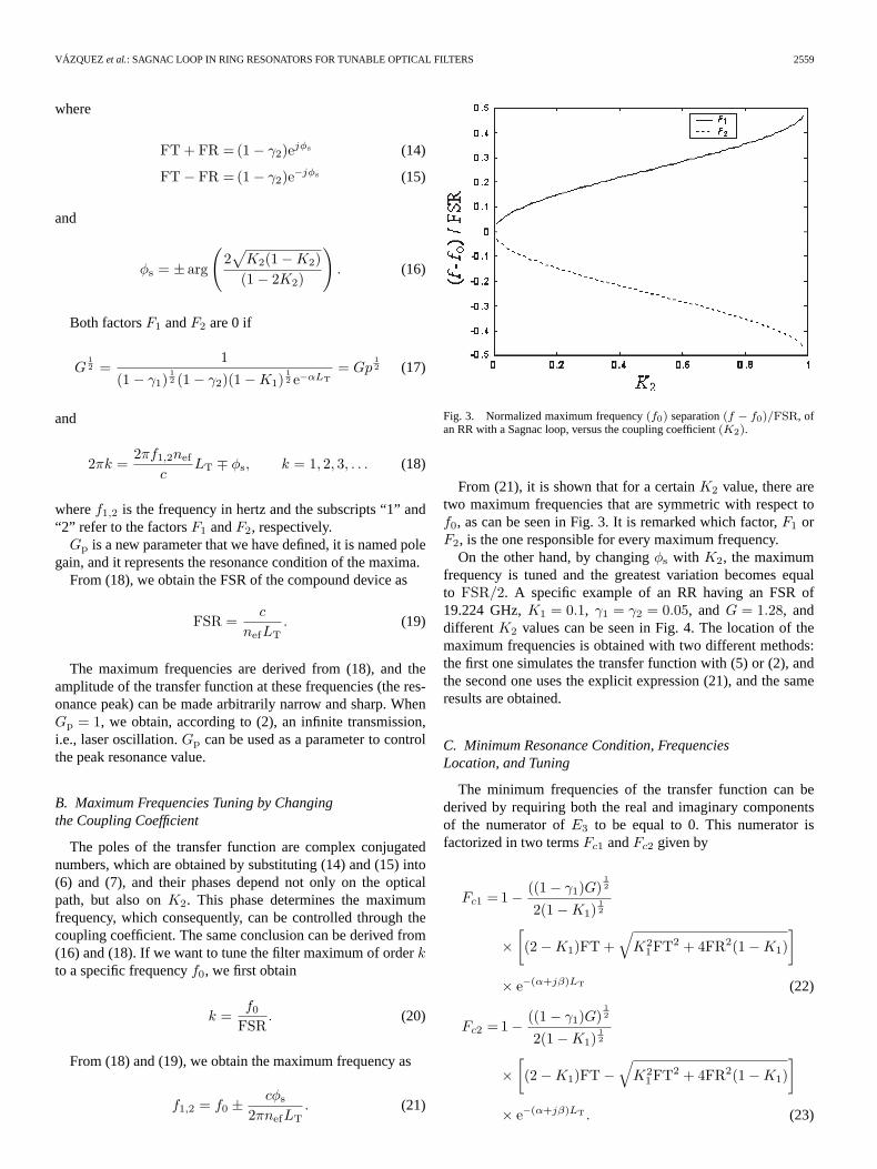
Fig. 3. Normalized maximum frequency (f0) separation (f − f0)/FSR, ofan RR with a Sagnac loop, versus the coupling coefficient (K2).
From (21), it is shown that for a certain K2 value, there aretwo maximum frequencies that are symmetric with respect tof0, as can be seen in Fig. 3. It is remarked which factor, F1 orF2, is the one responsible for every maximum frequency.
On the other hand, by changing φs with K2, the maximumfrequency is tuned and the greatest variation becomes equalto FSR/2. A specific example of an RR having an FSR of19.224 GHz, K1 = 0.1, γ1 = γ2 = 0.05, and G = 1.28, anddifferent K2 values can be seen in Fig. 4. The location of themaximum frequencies is obtained with two different methods:the first one simulates the transfer function with (5) or (2), andthe second one uses the explicit expression (21), and the sameresults are obtained.
C. Minimum Resonance Condition, FrequenciesLocation, and Tuning
The minimum frequencies of the transfer function can bederived by requiring both the real and imaginary componentsof the numerator of E3 to be equal to 0. This numerator isfactorized in two terms Fc1 and Fc2 given by
Fc1 = 1 − ((1 − γ1)G)12
2(1 − K1)12
×[(2 − K1)FT +
√K2
1FT2 + 4FR2(1 − K1)]
× e−(α+jβ)LT (22)
Fc2 = 1 − ((1 − γ1)G)12
2(1 − K1)12
×[(2 − K1)FT −
√K2
1FT2 + 4FR2(1 − K1)]
× e−(α+jβ)LT . (23)

2560 JOURNAL OF LIGHTWAVE TECHNOLOGY, VOL. 23, NO. 8, AUGUST 2005
Fig. 4. Tuning of the transfer function of the active RR with a Sagnac loop: K1 = 0.1, γ1 = γ2 = 0.05, G = 1.28, and for K2 values of (a) 0, (b) 0.25,(c) 0.50, (d) 0.75, or (e) 1.
At port E′r1 , the numerator is a polynomial of first order with
a constant phase, so there are no tuning zero frequencies.The second term of (22) has a radical that is equal in both
factors and can be positive or negative. Our aim is to obtain aphase dependence different to the optical path, so this second
term must be a complex number. Substituting FR and FT with(10) and (11), respectively, the radical is negative if
K1 < −8A + 4√
4A2 + A (24)
VÁZQUEZ et al.: SAGNAC LOOP IN RING RESONATORS FOR TUNABLE OPTICAL FILTERS 2561
where
A =K2(1 − K2)(1 − 2K2)2
. (25)
For K2 values close to 0.5, it is greater the range of K1
values that gives complex numbers. Substituting K2 with 1 −K2 in (25), the same A value is obtained.
Assuming the designed device follows (24) and (25), thefactors Fc1 and Fc2 are 0 if
G12 =
1(1 − γ1)
12 (1 − γ2)e−αLT
= G12c = G
12p
√1 − K1
(26)
and
2πm =2πfz1,2nef
cLT ∓ φz, m = 1, 2, 3, . . . (27)
where
φz = φz1 = −φz2
= arg
(√−K2
1 (1 − 2K2)2 + 16(1 − K1)(1 − K2)K2
(2 − K1)(1 − 2K2)
).
(28)
In these expressions, φz1, φz2 are the phases and fz1, fz2 arethe minimum frequencies (the “1” and “2” subscripts refer tothe factor Fc1 and Fc2, respectively).
Gc is a new parameter that we define, which represents theminimum resonance condition and is named the zero gain.The condition shown in (26), known in the microwave field ascritical coupling, is due to a perfect destructive interference.
From (27) and (28), we see that tuning of the minimumfrequencies is controlled through K1 and K2. A wider tuningrange is obtained for K2 close to 1, with K1 small, and aworse tuning is achieved for K1 close to 0 and K2 close to 0,or if K1 is close to 1 and K2 approaches 0.5 (from K2 < 0.5).As a general rule, we select a small and fixed K1 value, and weuse K2 for tuning the device. Each minimum can be tuned upto FSR/2.
An example of the tuning process with K2 is shown in Fig. 5for a G value close to the Gc condition in (26): K1 = 0.4,FSR = 19.224 GHz, γ1 = γ2 = 0.05, and G = 1.13. K1 andK2 values follow those of (24).
IV. FILTER APPLICATIONS AND
DEVICE PARAMETERS
The active RR with the Sagnac loop can have different filterapplications depending on device parameters, such as gain,
coupling coefficients, and losses. Because the transfer functionat port E3 have poles and zeros, or frequencies at which theamplitude goes ideally to 0 or infinity, we can have channel-dropping or selective filters at that port. The resonance condi-tions are different in each case, in the phase and in the amplitudeconditions, so they will be used to discern between them.
The resonance conditions for the transfer function at port 3are given by the pole and zero gains, which are plotted versusthe K1 and G values, with K2 as a parameter, at Fig. 6. It canbe seen that Gp is always greater than any Gc value, as it canalso be derived from (26). Gp only depends on the K1 value.Gc is independent of K1 and K2 if (24) is fulfilled. In this case,the device has two complex conjugated zeros or two minimumfrequencies that are symmetric with respect to the minimumfrequency of the device with no reflections (K2 = 0), and thereis a unique resonance condition for both minimum frequenciesGc. A specific example is reported in Fig. 5, for K1 = 0.4,which corresponds to the straight line shown in Fig. 6, forany K2 value. But if (24) is not followed, there are differentresonance conditions depending on the Fc1,2 factor, which is0. This corresponds in Fig. 6 with the divergence in the Gc
curve at a certain point, so Gc1,2 are obtained; for example,at K1 = 0.6 for K2 = 0.05. The Gc1,2 curves for any K2 valueare equal for the corresponding 1 − K2 value, because the sameA value is obtained for any of them in (25).
In any case, the filter is stable if the transfer function polesare located inside the unit circle; from (6), (14), and (26), it isderived that this condition is fulfilled if G < Gp.
The output power is obtained by substituting (10) and (11)in either (2) or (5). In the particular case of selecting K1
and K2 values following (24) and after some simplifications,the expression is of (29), shown at the bottom of the page,with
A0|C| =√
(1 − γ1)(1 − γ2)√
Ge−αLT
=√
G
Gc(30)
D0 =√
(1 − γ1)(1 − K1)(1 − γ2)√
Ge−αLT
=
√G
Gp. (31)
A. Designing a Selective Filter
In order to have a selective filter with a sharp responseand tunable through the coupling coefficient K2, the valuesof the parameters K1 and G must be those that make theratio Gp/G close to 1 but still produce a stable filter, whichmeans the gain must always be lower than the pole gain. An
∣∣∣∣E3
E1
∣∣∣∣2
=
(1 + A2
0|C|2)2
(1 − 2 A0|C|
1+A20|C|2 cos(−βLT + φZ)
) (1 − 2 A0|C|
1+A20|C|2 cos(−βLT − φZ)
)(1 + D2
0)2(1 − 2 D0
1+D20
cos(−βLT + φs)) (
1 − 2 D01+D2
0cos(−βLT − φs)
) (29)

2562 JOURNAL OF LIGHTWAVE TECHNOLOGY, VOL. 23, NO. 8, AUGUST 2005
Fig. 5. Tuning of the transfer function of the active RR with a Sagnac loop: K1 = 0.4, γ1 = γ2 = 0.05, G = 1.13, and for K2 values of (a) 0, (b) 0.25,(c) 0.50, or (d) 0.75.
example is reported in Fig. 4 for K1 = 0.1, γ1 = γ2 = 0.05,and G = 1.28, and different K2 values from 0 to 0.5. In thiscase Gp = 1.3 (see Fig. 6).
The overall losses of the compound device control the full-width at half-maximum (FWHM) and the amplitude of themaximum. As an example, considering a specific design withK1 and K2 values making φsφz ∼ 0, the amplitude of themaximum output power in (29) is given by
∣∣∣∣E3
E1
∣∣∣∣2
max
=
( √Gc −
√G√
Gp −√
G
)2 (Gp
Gc
)2
. (32)
On the other hand, the FWHM bandwidth of the selective fil-ter ∆f is obtained by finding the detuning where the maximumpower in (32) decreases to half its value [5]. In deriving theFWHM, the output power is used. This is given by (29) andthe approximation near resonances. In the high finesse case,cos(θ) ∼ 1 − 1/2 θ2. By assuming K1 and K2 values, this
relationship becomes φs ∼ φz ∼ 0. This procedure yields
∆f =FSR
π
(1 − D0)√D0
(33)
where we can see that the FWHM is independent of K2.The finesse can be obtained in a straightforward manner
from the previous expression.
B. Designing a Notch Filter
On the other hand, in designing a notch filter, the ratio Gc/Gmust be close to 1. Tuning can be achieved through the couplingcoefficients K1 and K2, but K2 values must be within the rangeimposed by (24) for a specific K1 value. In this case, the devicewill always be stable. An example can be seen in Fig. 5, withK1 = 0.4, γ1 = γ2 = 0.05, and G = 1.13, and with differentK2 values from 0 to 0.5. In this case, Gp = 1.8 > G.
In our equations, we have considered the losses and apossible gain for compensating the losses or for giving more

VÁZQUEZ et al.: SAGNAC LOOP IN RING RESONATORS FOR TUNABLE OPTICAL FILTERS 2563
Fig. 6. Pole and zero gains, Gp and Gc, versus K1 with K2 as a parameter.γ1 = γ2 = 0.05, of the normalized transfer function at port E3, for the activeRR with a Sagnac loop.
Fig. 7. Output power versus frequency of the RR with a Sagnac Loop:K1 = 0.92, K2 = 0.75 and, G in legend represents total loss or gain effectso including e−2αLT , γ1, γ2, and power gain.
flexibility to the designs. The effect of losses is very relevant;it has been shown that, depending on the relation between G,Gc, and Gp, it is possible to have a selective or notch filter.FWHM and minimum/maximum amplitude are also dependenton losses. Even resonance frequencies can be affected by thisparameter, if having great losses. This effect can be seen inthe example shown in Fig. 7, where the output power versusfrequency for K1 = 0.92, γ1 = γ2 = 0.075, K2 = 0.75, anddifferent losses, are plotted. It can be seen that the two minimaare quite close, so they can be distinguished only if gains closeto Gc are used. In this case, from (26), a Gc = 1.26 is obtained,so the minima going away from this value are not shown.
C. Dispersion Properties
Potential degrading effects of a filter cascade are the dis-persion problems caused by nonlinear filter phase responses
[2], [38]. On the other hand, these filters are used in some casesas dispersion compensators [4]. In any case, it is very importantto know the dispersion properties of the filter. For the specificconditions reported in (24), the output power is given by (29)and in the z-transform domain, the transfer function can beexpressed as
E3
E1= K0z
−22∏
i=1
[(z − Zci)
(1 − Zpiz−1)
](34)
where K0 is a constant.The differentiation of the transfer function phase with respect
to ω gives the group-delay time of the filter, using (29) and (34),under the conditions imposed by (24), the following expressionis obtained:
τ = τ0
2∑i=1
rci
cos(−βLT + (−1)iφz
)− rci
1 − 2rci cos (−βLT + (−1)iφz) + r2ci
−2∑
i=1
rpi
cos(−βLT + (−1)iφs
)− rpi
1 − 2rpi cos (−βLT + (−1)iφs) + r 2pi
(35)
with
rci =√
G
Gc; rpi =
√G
Gp∀i; τ0 =
1FSR
. (36)
Dispersion measures the rate of change of the group-delaywith respect to wavelength. The per-unit length dispersion isdefined as
D = L−1T
∂τ
∂λ= − 2πc
λ2L2T
τo∂τ
∂β(37)
which can be calculated from (35).A proper selection of the location of the poles and zeros
allows for the control of filter dispersion.In Fig. 8, the group-delay time for the selective filter pre-
viously designed is shown, the tuning of which is shown inFig. 4. In Fig. 8(a), the group-delay time is shown as a functionof frequency and K2 at a fixed value of K1, G, and losses.The fixed values are the same as those for Fig. 4. The processof how the group-delay, and consequently, the dispersion, istuned is clearly visible in Fig. 8(b), where the group-delaytime of Fig. 8(a) is shown for five specific K2 values: K2 = 0,K2 = 0.25, K2 = 0.50, K2 = 0.75, and K2 = 1.
The group-delay time for the notch filter previously designedis shown in Fig. 9. It is plotted as a function of frequency, ata fixed value of K1, G, and losses, and the parameter is K2.The fixed and the K2 parameter values are the same as thosefor Fig. 5.
In Fig. 10, the group-delay time of a device as a functionof frequency is plotted. The device has a positive and negativevalue and sharp and smooth responses, depending on the pa-rameter K2. The fixed values are K1 = 0.9, and overall powerlosses of 0.25 (G = 0.25, γ1 = γ2 = 0 = α).

2564 JOURNAL OF LIGHTWAVE TECHNOLOGY, VOL. 23, NO. 8, AUGUST 2005
Fig. 8. (a) Group-delay time of the active RR with a Sagnac loop as a functionof frequency and K2 at a fixed value of K1, G, and losses. The fixed values arethe same as those for Fig. 4. (b) Group-delay time of (a) for five specific K2
values: 0, 0.25, 0.50, 0.75, and 1.
D. Coupling-Ratio Tolerance Effect on Tuning
The study of tolerance is very important because it helpsus estimate the specific tolerance of implemented devices,depending on the basic elements that they are made of. Astudy of parameter variation influence on design specificationsfor an RR-based device is reported in [7]; fabrication toler-ances and temperature effects on design specifications and onworking wavelength are taken into account, and some specificvalues using fiber technology are included. But nothing is saidabout coupling-ratio accuracy on wavelength tuning, which isgoing to be described here for the RR with a Sagnac loopconfiguration.
The tolerance study is usually made around a working designpoint, which will be defined by the subscript q. The resonantfrequency location, obtained from (18) in a selective filter andfrom (27) in a notch filter, depends on temperature throughLT, and nef as in any RR, but it also depends on K2 andK1. The accuracy on these coupling coefficients determines theresonant frequency location accuracy, and this dependence is
Fig. 9. Group-delay time of an RR with a Sagnac loop as a function offrequency, at a fixed value of K1, G, and losses, and the parameter is K2.The fixed and the K2 parameter values are the same as those for Fig. 5.
Fig. 10. Group-delay time (picosecond) of the RR with a Sagnac loop as afunction of frequency: K1 = 0.9, G = 0.25, γ1 = γ2 = α = 0, and with K2
as a parameter.
given by
|∆f1,2| =(
∂f1,2
∂K2
)∆K2 +
(∂f1,2
∂K1
)∆K1. (38)
For the selective filter, from (16) and (18), it can be seen thatonly the first term is not equal to 0 and the resonance frequencyaccuracy is given by
|∆f1,2| =FSR2π
(∂φs
∂K2
)∆K2 (39)
with ∣∣∣∣ ∂φs
∂K2
∣∣∣∣ =
(1
(1 − 2K2)2√
K2(1 − K2)
). (40)
The previously mentioned relationship becomes more crit-ical if K2 is close to 0.5, 0, and 1. For example, for K2 =0.49 and ∆K2 = 0.001, relative deviation (1/φsq × ∆K2 ×

VÁZQUEZ et al.: SAGNAC LOOP IN RING RESONATORS FOR TUNABLE OPTICAL FILTERS 2565
[δφs/δK2]q × 100) is less than 10%, while for K2 = 0.3 it isless than 0.6%.
For the notch filter, from (27) and (28), it can be seen thatboth terms of (38) are now not equal to 0, and the resonancefrequency accuracy is given by
|∆f1,2| =FSR2π
[(∂φz
∂K2
)∆K2 +
(∂φz
∂K1
)∆K1
](41)
with (42) and (43), shown at the bottom of the page.In this case, the worst accuracy is again obtained for K2
values close to 0.5. On the other hand, one term is positive andthe other is negative, so the accuracy is smaller than the biggerterm. The dominant effect always comes from K2 tolerances,which is clear if K1 tends to 0; if K1 tends towards 1, and(24) must be fulfilled so that this happens for K2, values closeto 0.5 and the denominator of (43) have a square term in(1 − 2K2), so again, it is dominant. For example, for K2 =K1 = 0.49 and ∆K2 = ∆K1 = ∆K = 0.001, relative devia-tion (1/φzq × [(δφz/δK2 + δφz/δK1) × ∆K]q × 100) is lessthan 10%, while for K2 = 0.3, it is less than 0.59%.
V. CONCLUSION
Novel filter architecture based on co- and counterpropagationsignals are presented. Equations describing the output fieldfrequency response for the different design parameters arereported. The same expressions are derived using two differenttechniques, the matrix formalism and the z-transform tech-nique. They are particularized for a specific architecture madeof a Sagnac loop in an RR. The multireflections originated bythe loop are controlled through the gain or losses and through acoupling coefficient that is responsible for the tuning. Simpleequations for designing and tuning are reported, along withrules for designing tunable selective or notch filters. The effectof losses (waveguide and coupler losses and optionally opticalgain), the filter dispersion properties, and the coupler coefficienttolerances on resonant frequency accuracy are also discussed.
The compound device analyzed has some physical character-istics similar to the RR ones that can be exploited in photonicapplications, which are complemented with the property ofbeing tunable with the coupling coefficient under specific de-sign conditions. These properties are its notch filter amplitudecharacteristics near critical coupling, and the magnification ofthe signal amplitude circulating in the ring, which is associatedwith energy storage. The last one can be used in designing
laser oscillators. Using the standard method of photonic filtersynthesis, the compound device can be used for designing fre-quency filters of different orders and dispersion compensationfilters.
Previous measurements on passive notch filter in fiber-optic technology validate the expressions derived and the noveltuning principle. The structure can be developed using inte-grated optics technologies.
APPENDIX ACOMPOUND RR USING THE MATRIX FORMALISMS
The filter architecture is shown in Fig. 1. The transfer-matrix method is used for calculating the transfer function ofa compound device that is made of concatenated elementarydevices; in our filter, the decomposition used is shown in Fig. 2.In the following, we are going to describe the expressions of thedifferent matrices involved.
The coupler transmission matrix is given by
[ac] =[ 1
tac− rac
tac
rac
tac
t2ac−r2ac
tac
](A1)
tac = j [(1 − γ1)K1]12 (A2)
rac = [(1 − γ1)(1 − K1)]12 (A3)
where K1 and γ1 are the coupling coefficient and the excessloss of the input coupler, respectively.
The transfer matrix of the waveguides and the transmissionfunctions within them are given by
[g] =[
ΠTxie(α+jβ)la 0
0 ΠTyie−(α+jβ)(LT−la)
](A4)
where α and β are the waveguide attenuation and the propaga-tion constant, respectively, LT is the total waveguide length,la is the waveguide length connecting the input coupler andthe TRF (see Fig. 1) and ΠN
1 (Txi) and ΠM
1 (Tyi) are the N
transmission transfer functions between the input coupler andthe TRF and the M transmission transfer functions between theTRF and the input coupler, respectively.
The TRF transfer matrix is given by
[TRF] =[ 1
FR −FTFR
FTFR
FR2−FT2
2
]. (A5)
∣∣∣∣ ∂φz
∂K2
∣∣∣∣ =
(8(1 − K1)
(1 − 2K2)2(2 − K1)√
−K21 (1 − 2K2)2 + 16(1 − K1)(1 − K2)K2
)(42)
∣∣∣∣ ∂φz
∂K1
∣∣∣∣ =
(−2K1
(1 − 2K2) (2 − K1)2√
−K21 (1 − 2K2)2 + 16(1 − K1)(1 − K2)K2
)(43)

2566 JOURNAL OF LIGHTWAVE TECHNOLOGY, VOL. 23, NO. 8, AUGUST 2005
It represents a general TRF, and not only a symmetric dis-continuity as in [13].
The transfer matrices of the original elements and theirmirror images are equals [g] = [g′] and [ac] = [ac′].
APPENDIX BCOMPOUND RR USING THE z-TRANSFORM TECHNIQUE
The filter architecture is shown in Fig. 1. In deriving thetransfer function in z at output port E3, we use the followingequations, considering the TRF placed at the middle of the ring:
E3 = (1 − γ1)12
[(1 − K1)
12 E1 + jK
121 E2
](B1)
E4 = (1 − γ1)12
[jK
121 E1 + (1 − K1)
12 E2
](B2)
E2 =M∏i=1
Tyi· z−1
[N∏
i=1
Txi· FT · E4 +
M∏i=1
Tyi· FR · E2b
]
(B3)
E2b = (1 − γ1)12 (1 − K1)
12 E4b (B4)
E4b =N∏
i=1
Txi· z−1
[M∏i=1
Tyi· FT · E2b +
N∏i=1
Txi· FR · E4
]
(B5)
where FR and FT are the transfer functions in reflection and intransmission, respectively, of the TRF, and z−1 represents theunit delay related to LT.
Combining the previous equations, the transfer function atport E3 reported in (5) is obtained.
ACKNOWLEDGMENT
The authors would like to thank Prof. O. Schwelb for fruitfulcomments.
REFERENCES
[1] G. Rossi, O. Jerphagnon, B. Olsson, and D. J. Blumenthal, “Optical SCMdata extraction using a fiber-loop mirror for WDM network systems,”IEEE Photon. Technol. Lett., vol. 12, no. 7, pp. 897–899, Jul. 2000.
[2] G. Lenz, B. J. Eggleton, C. R. Giles, C. K. Madsen, and R. E. Slusher,“Dispersive properties of optical filters for WDM systems,” IEEE J.Quantum Electron., vol. 34, no. 8, pp. 1390–1402, Aug. 1998.
[3] D. Sadot and E. Boimovich, “Tunable optical filters for dense WDMnetworks,” IEEE Commun. Mag., vol. 36, no. 12, pp. 50–55, Dec. 1998.
[4] C. K. Madsen and J. H. Zhao, Optical Filter Design and Analysis, A SignalProcessing Approach. New York: Wiley, 1999.
[5] O. Schwelb, “Transmission, group delay, and dispersion in single-ringoptical resonators and add/drop filters—a tutorial overview,” J. Lightw.Technol., vol. 22, no. 5, pp. 1380–1394, May 2004.
[6] N. Ngo and L. N. Binh, “Novel realization of monotonic butterworth-typelowpasss, highpass, and bandpass optical filters using phase-modulatedfiber-optic interferometers and ring resonators,” J. Lightw. Technol.,vol. 12, no. 5, pp. 827–840, May 1994.
[7] C. Vázquez, S. Vargas, and J. M. S. Pena, “Design and tolerance analysisof a router using an amplified ring resonator and Bragg gratings,” Appl.Opt., vol. 39, no. 12, pp. 1934–1940, 2000.
[8] R. Grover, V. Van, T. A. Ibrahim, P. P. Absil, L. C. Calhoun, F. G. Johnson,J. V. Hryniewicz, and P.-T. Ho, “Parallel-cascaded semiconductor micror-ing resonators for high-order and wide-FSR filters,” J. Lightw. Technol.,vol. 20, no. 5, pp. 900–905, May 2002.
[9] S. A. Havstad, B. Fischer, A. E. Willner, and M. G. Wickham, “Loop-mirror filters based on saturable-gain or -absorber gratings,” Opt. Lett.,vol. 24, no. 21, pp. 1466–1468, 1999.
[10] J. E. Heebner, P. Chak, S. Pereira, J. E. Sipe, and R. W. Boyd, “Distributedand localized feedback in microresonator sequences for linear and nonlin-ear optics,” J. Opt. Soc. Amer., B, Opt. Phys., vol. 21, no. 10, pp. 1818–1832, 2004.
[11] B. E. Little et al., “Very high-order microring resonator filters for WDMapplications,” IEEE Photon. Technol. Lett., vol. 16, no. 10, pp. 2263–2265, Oct. 2004.
[12] C. Vázquez, F. Hernández-Gil, and M. López-Amo, “Tunable ring res-onator filter for OFDM transmission systems,” Microw. Opt. Technol.Lett., vol. 8, no. 6, pp. 321–323, Apr. 1995.
[13] R. W. Boyd and J. E. Heebner, “Sensitive disk resonator photonic biosen-sor,” Appl. Opt., vol. 40, no. 31, pp. 5742–5747, 2001.
[14] J. E. Heebner and R. W. Boyd, “Enhanced all-optical switching by use ofa nonlinear fiber ring resonator,” Opt. Lett., vol. 24, no. 12, pp. 847–849,1999.
[15] P. Urquhart, “Compound optical-fiber-based resonators,” J. Opt. Soc.Amer. A, vol. 5, no. 6, pp. 803–812, 1988.
[16] J. Zhang and J. W. Y. Lit, “Compound fiber ring resonator: theory,” J. Opt.Soc. Amer. A, vol. 11, no. 6, pp. 1867–1873, 1994.
[17] ——, “All fiber compound ring resonator with a ring filter,” J. Lightw.Technol., vol. 12, no. 7, pp. 1256–1262, Dec. 1994.
[18] O. Schwelb and I. Frigyes, “All-optical tunable filters built withdiscontinuity-assisted ring resonators,” J. Lightw. Technol., vol. 19, no. 3,pp. 384–386, Mar. 2001.
[19] S. Vargas, C. Vázquez, and J. M. S. Pena, “Wide tunable filters using arecirculating delay line with multi-reflections,” Opt. Eng., vol. 41, no. 5,pp. 926–927, 2002.
[20] ——, “Novel tunable optical filter employing a fiber loop mirror forsynthesis applications in WDM,” in 14th Annu. Meeting IEEE Lasers andElectro-Optics Society, San Diego, CA, 2001, vol. II, pp. 899–900.
[21] C. Vázquez, S. Vargas, J. M. S. Pena, and P. Corredera, “Tunable opti-cal filters using compound ring resonators for DWDM,” IEEE Photon.Technol., vol. 15, no. 8, pp. 1085–1087, Aug. 2003.
[22] V. M. Menon, W. Tong, F. Xia, C. Li, and S. R. Forrest, “Nonreciproc-ity of counterpropagating signals in a monolithically integrated Sagnacinterferometer,” Opt. Lett., vol. 29, no. 5, pp. 513–515, 2004.
[23] D. G. Rabus, M. Hamacher, U. Troppenz, and H. Heidrich, “High-Qchannel-dropping filters using ring resonators with integrated SOAs,”IEEE Photon. Technol. Lett., vol. 14, no. 10, pp. 1442–1444, Oct.2002.
[24] V. M. Menon, W. Tong, and S. R. Forrest, “Control of quality factorand critical coupling in microring resonators through integration of asemiconductor optical amplifier,” IEEE Photon. Technol., vol. 16, no. 5,pp. 1343–1345, May 2004.
[25] K. Oda, S. Suzuki, H. Takahashi, and H. Toba, “An optical FDMdistribution experiment using a high finesse waveguide-type doublering resonator,” IEEE Photon. Technol., vol. 6, no. 8, pp. 1031–1034,Aug. 1994.
[26] D. G. Rabus and M. Hamacher, “MMI-coupled ring resonators inGaInAsP–InP,” IEEE Photon. Technol., vol. 13, no. 8, pp. 812–814,Aug. 2001.
[27] A. Melloni, R. Costa, P. Monguzzi, and M. Martinelli, “Ring-resonatorfilters in silicon oxynitride technology for dense wavelength-division mul-tiplexing systems,” Opt. Lett., vol. 28, no. 17, pp. 1567–1569, 2003.
[28] D. K. Armani, T. J. Kippenberg, S. M. Spillane, and K. J. Vahala, “Ultra-high-Q toroid microcavity on a chip,” Nature, vol. 421, no. 6926, pp. 925–928, 2003.
[29] K. Djordjev, S. Choi, S. Chou, and P. Dapkus, “Microdisk tunable resonantfilters and switches,” IEEE Photon. Technol. Lett., vol. 14, no. 6, pp. 828–830, Jun. 2002.
[30] B. E. Little et al., “Very high-order microring resonator filters for WDMapplications,” IEEE Photon. Technol. Lett., vol. 16, no. 10, pp. 2263–2265, Oct. 2004.
[31] K. Djordjev, S. Choi, S. Chou, and P. Dapkus, “Vertically coupled InPmicrodisk switching devices with electroabsorptive active regions,” IEEEPhoton. Technol. Lett., vol. 14, no. 8, pp. 1115–1117, Aug. 2002.
[32] M. M. Lee and M. C. Wu, “A MEMS-actuated tunable microdisk res-onator,” in IEEE Int. Conf. Optical Microelectromechanical Systems(MEMS), Waikoloa, HI, 2003, pp. 28–29, MC3.
[33] W. M. J. Green, R. K. Lee, A. Yariv, and M. A. Scherer, “Control ofoptical waveguide-resonator coupling: Application to low-power opticalmodulation and switching,” in IEEE Lasers and Electro-Optics Society(LEOS) Annu. Meeting Conf. Proc., Tucson, AZ, 2003, vol. 1, pp. 130–131. MM3.

VÁZQUEZ et al.: SAGNAC LOOP IN RING RESONATORS FOR TUNABLE OPTICAL FILTERS 2567
[34] W. M. J. Green, R. K. Lee, G. A. DeRose, A. Scherer, and A. Yariv,“Hybrid InGaAsP–InP Mach–Zehnder racetrack resonator for thermoop-tic switching and coupling control,” Opt. Express, vol. 13, no. 5, pp. 1651–1659, 2005.
[35] R. H. Qu, H. Zhao, Z. J. Fang, E. Marin, and J. P. Meunier, “Configurablewavelength-selective switch based on fiber grating and fiber loop mirror,”IEEE Photon. Technol., vol. 12, no. 10, pp. 1343–1345, Oct. 2000.
[36] X. Shu, S. Jiang, and D. Huang, “Fiber grating Sagnac loop and itsmultiwavelegth-laser,” IEEE Photon. Technol., vol. 12, no. 8, pp. 980–982, Aug. 2000.
[37] I. Golub and E. Simova, “Ring resonator in a Sagnac interferometer as abirefringence magnifier,” Opt. Lett., vol. 30, no. 1, pp. 87–89, 2005.
[38] J. D. Downie and A. B. Ruffin, “Analysis of signal distortion and crosstalkpenalties induced by optical filters in optical networks,” J. Lightw.Technol., vol. 21, no. 9, pp. 1876–1886, Sep. 2003.
Carmen Vázquez (M’99) was born in Madrid, Spain, on May 1968. Shereceived the M.S. degree in physics (electronics) from Complutense Universityof Madrid, Madrid, Spain, in 1991 and the Ph.D. degree from the Telecommuni-cations Engineering School, Polytechnic University of Madrid (UPM), Madrid,Spain, in 1995.
She enjoyed a fellowship at TELECOM, Denmark, in 1991, working onerbium-doped fiber amplifiers. From 1992 to October 1995, she worked atthe Optoelectronics Division of Telefónica Investigación y Desarrollo, Madrid,Spain. She was involved in III–V integrated optics devices characterization,design, and fabrication. In October 1995, she joined University Carlos IIIof Madrid, Madrid, Spain, where she is currently working as an AssociateProfessor and Head of the Electronics Technology Department. Her currentwork includes the design of fiber optics, liquid crystals (LC), and integratedoptic devices, and their application to optical communications, instrumentation,and sensor networks.
Dr. Vázquez is a Member of The International Society for Optical Engineers(SPIE), Optical Society of America (OSA), and Sociedad Española de Óptica(SEDO).
Salvador Elías Vargas was born in Panamá, in 1973. He received the M.S.degree in electrical and electronic engineering from Universidad Tecnológicade Panamá, Panama, in 1996, and the Ph.D. degree at University Carlos III ofMadrid, Madrid, Spain, in December 2003.
He was an Assistant Professor in Universidad Tecnológica de Panamá,Panama, from January to September of 1997. In October 1997, he enjoyed afellowship from the Spanish International Cooperation Agency to do studies inCarlos III University of Madrid, Madrid, Spain. He is currently an AssistantProfessor in the Electronics Department of Carlos III University of Madrid,Madrid, Spain. His main research interests include synthesis of photonic filters,tunable photonic filters, liquid crystals (LC), and polarization devices, and theirapplications to optical communications.
José Manuel Sánchez Pena (A’95–SM’03) received the M.S. and Ph.D.degrees in telecommunication engineering from the Polytechnic University ofMadrid, Madrid, Spain, in 1988 and 1993, respectively.
He was a Visiting Researcher at Exeter University, Devon, U.K., fromFebruary to September of 1993. In March 1995, he joined University CarlosIII of Madrid, Madrid, Spain, where he is currently an Associate Professorand Head of the Displays and Photonic Applications Group of the ElectronicTechnology Department. His main research interests include electroopticalcharacterization of liquid-crystal displays, design of optical sensors and op-toelectronic instrumentation for rehabilitation technology applications, andoptical communications.
Dr. Pena is a Member of The International Society for Optical Engineers(SPIE), International Liquid Crystal Society (ILCS), and International Societyfor Augmentative & Alternative Communication (ISAAC).

![Electrically Tunable Open Split-Ring Resonators based on .... Tunable Metam… · e.g. by the use of varactor diodes [3]. However, varactor diodes limit the operation frequency to](https://img.pdfslide.us/doc/110x75/5f31343356afe71a73122f38/electrically-tunable-open-split-ring-resonators-based-on-tunable-metam-eg.jpg)