Embed Size (px)
Citation preview

Safety Manual for Qorivva MPC5643L
Devices Supported:MPC5643L
MPC5643LSMRev. 2
04/2013
(NOTE: Replaces the Safety Application Guide for MPC5643L – MPC5643LSAG)

MPC5643LSMRev. 204/2013
Information in this document is provided solely to enable system and software
implementers to use Freescale products. There are no express or implied copyright
licenses granted hereunder to design or fabricate any integrated circuits based on the
information in this document.
Freescale reserves the right to make changes without further notice to any products
herein. Freescale makes no warranty, representation, or guarantee regarding the
suitability of its products for any particular purpose, nor does Freescale assume any
liability arising out of the application or use of any product or circuit, and specifically
disclaims any and all liability, including without limitation consequential or incidental
damages. “Typical” parameters that may be provided in Freescale data sheets and/or
specifications can and do vary in different applications, and actual performance may
vary over time. All operating parameters, including “typicals,” must be validated for each
customer application by customer’s technical experts. Freescale does not convey any
license under its patent rights nor the rights of others.
How to Reach Us:
Home Page: freescale.com
Web Support: freescale.com/support
Freescale, the Freescale logo, AltiVec, C-5, CodeTest, CodeWarrior, ColdFire, C-Ware,
Energy Efficient Solutions logo, Kinetis, mobileGT, PowerQUICC, Processor Expert,
QorIQ, Qorivva, StarCore, Symphony, and VortiQa are trademarks of Freescale
Semiconductor, Inc., Reg. U.S. Pat. & Tm. Off. Airfast, BeeKit, BeeStack, ColdFire+,
CoreNet, Flexis, MagniV, MXC, Platform in a Package, QorIQ Qonverge, QUICC
Engine, Ready Play, SafeAssure, SMARTMOS, TurboLink, Vybrid, and Xtrinsic are
trademarks of Freescale Semiconductor, Inc. All other product or service names are
the property of their respective owners. The Power Architecture and Power.org
word marks and the Power and Power.org logos and related marks are
trademarks and service marks licensed by Power.org.
© 2013 Freescale Semiconductor, Inc.
Safety Manual for Qorivva MPC5643L, Rev. 1
Freescale Semiconductor3
Table of Contents1 Preface. . . . . . . . . . . . . . . . . . . . . . . . . . . . . . . . . . . . . . . . . . . . 4
1.1 Related documents . . . . . . . . . . . . . . . . . . . . . . . . . . . . . . 51.2 Vocabulary . . . . . . . . . . . . . . . . . . . . . . . . . . . . . . . . . . . . 6
2 General information . . . . . . . . . . . . . . . . . . . . . . . . . . . . . . . . . 72.1 Assumed conditions of operation . . . . . . . . . . . . . . . . . . . 72.2 Safety function . . . . . . . . . . . . . . . . . . . . . . . . . . . . . . . . . 72.3 Safe state . . . . . . . . . . . . . . . . . . . . . . . . . . . . . . . . . . . . . 72.4 Single-point Fault Tolerant Time Interval and Process
Safety Time. . . . . . . . . . . . . . . . . . . . . . . . . . . . . . . . . . . . 92.5 Latent Fault Tolerant Time Interval (L-FTTI) for latent
faults . . . . . . . . . . . . . . . . . . . . . . . . . . . . . . . . . . . . . . . . 102.6 Failure handling. . . . . . . . . . . . . . . . . . . . . . . . . . . . . . . . 12
3 Functional safety concept . . . . . . . . . . . . . . . . . . . . . . . . . . . 133.1 Faults . . . . . . . . . . . . . . . . . . . . . . . . . . . . . . . . . . . . . . . 133.2 Failures . . . . . . . . . . . . . . . . . . . . . . . . . . . . . . . . . . . . . . 143.3 General functional safety concept. . . . . . . . . . . . . . . . . . 17
3.3.1 Sphere of Replication—Lockstep mode (LSM) . . . 19
4 System-level hardware requirements . . . . . . . . . . . . . . . . . . 204.1 Assumed functions by separate device. . . . . . . . . . . . . . 20
4.1.1 High-impedance outputs . . . . . . . . . . . . . . . . . . . . 214.1.2 External Watchdog (EXWD) . . . . . . . . . . . . . . . . . 214.1.3 Power Supply Monitor (PSM) . . . . . . . . . . . . . . . . 224.1.4 Error Out Monitor (ERRM). . . . . . . . . . . . . . . . . . . 22
4.2 Optional hardware measures on system level . . . . . . . . 244.2.1 PWM output monitor (PWMA). . . . . . . . . . . . . . . . 24
4.3 PowerSBC. . . . . . . . . . . . . . . . . . . . . . . . . . . . . . . . . . . . 25
5 System-level software requirements . . . . . . . . . . . . . . . . . . 275.1 Disabled modes of operation . . . . . . . . . . . . . . . . . . . . . 27
5.1.1 Debug mode . . . . . . . . . . . . . . . . . . . . . . . . . . . . . 275.1.2 Test mode . . . . . . . . . . . . . . . . . . . . . . . . . . . . . . . 28
5.2 MPC5643L modules . . . . . . . . . . . . . . . . . . . . . . . . . . . . 285.2.1 Fault Collection and Control Unit (FCCU) . . . . . . . 285.2.2 Reset Generation Module (MC_RGM) . . . . . . . . . 325.2.3 Self Test Control Unit (STCU) . . . . . . . . . . . . . . . . 325.2.4 Temperature Sensor (TSENS) . . . . . . . . . . . . . . . 335.2.5 Software Watchdog Timer (SWT) . . . . . . . . . . . . . 345.2.6 Redundancy Control Checking Unit (RCCU) . . . . 355.2.7 Cyclic Redundancy Checker Unit (CRC). . . . . . . . 355.2.8 Internal RC Oscillator (IRCOSC). . . . . . . . . . . . . . 375.2.9 Frequency-Modulated PLL (FMPLL) . . . . . . . . . . . 385.2.10 Clock Monitor Unit (CMU) . . . . . . . . . . . . . . . . . . . 395.2.11 Power Management Unit (PMU) . . . . . . . . . . . . . . 405.2.12 Memory Protection Unit (MPU) . . . . . . . . . . . . . . . 425.2.13 Built-in hardware self-tests (BIST). . . . . . . . . . . . . 435.2.14 Error correction (ECC, ECSM) . . . . . . . . . . . . . . . 445.2.15 Interrupt Controller (INTC) . . . . . . . . . . . . . . . . . . 465.2.16 Semaphore Unit (SEMA4). . . . . . . . . . . . . . . . . . . 465.2.17 Enhanced Direct Memory Access (eDMA) . . . . . . 46
5.2.18 Periodic Interrupt Timer (PIT) . . . . . . . . . . . . . . . .475.2.19 System Status and Configuration
Module (SSCM) . . . . . . . . . . . . . . . . . . . . . . . . . .475.2.20 Flash memory . . . . . . . . . . . . . . . . . . . . . . . . . . . .485.2.21 Cross Triggering Unit (CTU) . . . . . . . . . . . . . . . . .515.2.22 Fault injection tests . . . . . . . . . . . . . . . . . . . . . . . .535.2.23 SRAM . . . . . . . . . . . . . . . . . . . . . . . . . . . . . . . . . .545.2.24 Glitch filter . . . . . . . . . . . . . . . . . . . . . . . . . . . . . . .545.2.25 Register Protection Module (REG_PROT). . . . . . .545.2.26 Analog to Digital Converter (ADC) . . . . . . . . . . . . .55
5.3 I/O functions . . . . . . . . . . . . . . . . . . . . . . . . . . . . . . . . . .575.3.1 Digital inputs . . . . . . . . . . . . . . . . . . . . . . . . . . . . .585.3.2 Digital outputs . . . . . . . . . . . . . . . . . . . . . . . . . . . .645.3.3 Analog inputs . . . . . . . . . . . . . . . . . . . . . . . . . . . . .745.3.4 Other requirements . . . . . . . . . . . . . . . . . . . . . . . .82
5.4 Communications . . . . . . . . . . . . . . . . . . . . . . . . . . . . . . .825.4.1 Redundant communication . . . . . . . . . . . . . . . . . .825.4.2 Fault-tolerant communication protocol . . . . . . . . . .83
6 Failure rates and FMEDA . . . . . . . . . . . . . . . . . . . . . . . . . . . .846.1 Mission profile . . . . . . . . . . . . . . . . . . . . . . . . . . . . . . . . .846.2 Overview . . . . . . . . . . . . . . . . . . . . . . . . . . . . . . . . . . . . .856.3 Key metrics for basic chip elements . . . . . . . . . . . . . . . .87
7 Provisions against dependent failures . . . . . . . . . . . . . . . . .887.1 Causes of dependent failures . . . . . . . . . . . . . . . . . . . . .887.2 Measures against dependent failures . . . . . . . . . . . . . . .89
7.2.1 Physical isolation . . . . . . . . . . . . . . . . . . . . . . . . . .897.2.2 Environmental conditions. . . . . . . . . . . . . . . . . . . .907.2.3 Failures of common signals . . . . . . . . . . . . . . . . . .90
7.3 CMF avoidance on system level . . . . . . . . . . . . . . . . . . .917.3.1 I/O pin/ball configuration . . . . . . . . . . . . . . . . . . . .917.3.2 External timeout function . . . . . . . . . . . . . . . . . . .100
7.4 IC considerations . . . . . . . . . . . . . . . . . . . . . . . . . . . . .101
8 Additional information . . . . . . . . . . . . . . . . . . . . . . . . . . . . .1028.1 Safety function pseudo-code . . . . . . . . . . . . . . . . . . . . .102
8.1.1 Flash memory . . . . . . . . . . . . . . . . . . . . . . . . . . .1038.1.2 <module>_SWTEST_REGCRC . . . . . . . . . . . . .1058.1.3 CTU . . . . . . . . . . . . . . . . . . . . . . . . . . . . . . . . . . .1108.1.4 Digital inputs . . . . . . . . . . . . . . . . . . . . . . . . . . . .1228.1.5 Digital outputs . . . . . . . . . . . . . . . . . . . . . . . . . . .1248.1.6 Analog inputs . . . . . . . . . . . . . . . . . . . . . . . . . . . .130
8.2 Checks and configurations . . . . . . . . . . . . . . . . . . . . . .133
9 Further information. . . . . . . . . . . . . . . . . . . . . . . . . . . . . . . .1349.1 Acronyms and abbreviations . . . . . . . . . . . . . . . . . . . . .1349.2 Safety Application Guide tag differences. . . . . . . . . . . .135
10 Document revision history . . . . . . . . . . . . . . . . . . . . . . . . . .138

Safety Manual for Qorivva MPC5643L, Rev. 1
Freescale Semiconductor4

Preface
1 PrefaceThis document discusses requirements for the use of the MPC5643L Microcontroller Unit (MCU) in functional safety relevant applications requiring high functional safety integrity levels.
It is intended to support system and software engineers using the MPC5643L available features as well as achieving additional diagnostic coverage by software measures.
Several measures are prescribed as safety requirements whereby the measure described was assumed to be in place when analyzing the functional safety of this Microcontroller Unit (MCU). In this sense, requirements in the Safety Manual (SM) are driven by assumptions concerning the functional safety of the system that will integrate the MPC5643L.
• Assumption: An assumption being relevant for functional safety in the specific application under consideration (condition of use). It is assumed that the user fulfills an assumption in his design.
• Assumption under certain preconditions: An assumption being relevant under certain preconditions. It is assumed that the user fulfills an assumption in his design, if the associated precondition is met.
Example: Assumption: It is assumed that the recommended operating conditions given in the MPC5643L data sheet are maintained.
Example: Assumption under certain preconditions: If an output in high-impedance is not considered safe at system level, it is assumed that countermeasures are placed to bring the safety-critical outputs to their Safe state.
NOTEAssumptions (or assumptions under certain preconditions) are marked by a tag of the form “SM_nnn” at the beginning of the assumption, and are terminated with an “end”. Both of these tags are enclosed within square brackets for easy recognition. These tags could be used to allow importing the assumptions into safety traceability management tools.
For the use of the MCU this means that if a specific safety manual assumption is not fulfilled, it has to be rationalized that an alternative implementation is at least similarly efficient concerning the functional safety requirement in question (for example, provides same coverage, reduces the likelihood of Common Mode Failure (CMF) similarly well, and so on) or the estimation of an increased failure rate (SPF, RF, MPF, DU …) and reduced metrics (SFF: Safe Failure Fraction, SPFM: Single-Point Fault Metrics, LFM: Latent Fault Metric) due to the deviation has be specified.
This document also contains guidelines on how to configure and operate the MPC5643L for functional safety relevant applications requiring high functional safety integrity levels. These guidelines are preceded by one of the following text statements:
• Recommendation: A recommendation is either a proposal for the implementation of an assumption, or a reasonable measure which is recommended to be applied, if there is no assumption in place. The user has the choice whether or not to obey the recommendation.
• Rationale: The motivation for a specific assumption and/or recommendation.
Safety Manual for Qorivva MPC5643L, Rev. 2
Freescale Semiconductor 4

Preface
• Implementation hint: An implementation hint gives specific hints on the implementation of an assumption and/or recommendation on the MPC5643L. The user has the choice whether or not to obey the implementation hint.
These guidelines are considered to be useful approaches for the specific topics under discussion. The user will need to use discretion in deciding whether these measures are appropriate for their applications.
This document is valid only under the assumption that the MCU is used in functional safety applications requiring a fail-silent or a fail-indicate MCU. A fail-operational mode of the MPC5643L is not described.
This document targets high functional safety integrity levels. For functional safety goals that do not require high functional safety integrity levels, system integrators will need to tailor the requirements for their specific application.
It is assumed that the user of this document is in general familiar with the MPC5643L device, ISO 26262, and/or IEC 61508 standards.
This document is based on MPC5643LSAG, Safety Application Guide for Qorivva MPC5643L (Rev. 7) and is intended to be used as a replacement. The “Requirement” tag numbers in this document correspond to the “Mandatory” tag numbers of the Safety Application Guide [SAG_MPC5643L_number] as much as possible. Additional or missing tags are listed in Section 9.2, Safety Application Guide tag differences. The phrasing of the assumptions in this document is different from the phrasing of the mandatory requirements in the Safety Application Guide; however, the fundamentals are similar.
1.1 Related documentsThis section lists all the documentation mentioned in this safety manual:
• IEC 61508: IEC 61508 Functional safety of electrical/electronic/programmable electronic safety-related systems, international standard, ed. 2.0, April 2010
• ISO 26262: ISO 26262 Road vehicles—Functional safety, November 2011
• MPC5643LRM, Qorivva MPC5643L Microcontroller Reference Manual
• MPC5643L, Qorivva MPC5643L Microcontroller Data Sheet
• MPC5643L_REV3.1_2N89D, MPC5643L Mask Set Errata for Mask REV3.1_2N89D
• MPC5643LSAG, Safety Application Guide for Qorivva MPC5643L
• FMEDA
— Customer_Version_FMEDA
— Customer_Version_Clock_FMEDA
— Customer_Version_Flash_FMEDA
— Customer_Version_SRAM_FMEDA
— Peripheral_Failurerates
• Addressing the Challenges of Functional Safety in the Automotive and Industrial Markets, White Paper, October 2011
Safety Manual for Qorivva MPC5643L, Rev. 2
Freescale Semiconductor5

Preface
1.2 VocabularyThis document uses vocabulary defined in ISO 26262-1 and IEC 61508-4. The following terms are of particular importance:
• System: functional safety-related system that both implements the required functional safety goals necessary to achieve or maintain a Safe statesystem for the equipment under control (control system) and is intended to achieve, on its own or with other electrical/electronic/programmable electronic functional safety-related systems and other risk reduction measures, the necessary functional safety integrity for the required safety functions.
• System integrator: person who is responsible for the system integration.
• Element: part of a subsystem comprising a single component or any group of components (for example, hardware, software, hardware parts, software units) that performs one or more element safety functions (functional safety requirements).
• Trip time: the maximum time of operation of the MCU without switching to power down state.
Safety Manual for Qorivva MPC5643L, Rev. 2
Freescale Semiconductor 6

General information
2 General informationThe MPC5643L is designed to be used in automotive or industrial applications which need to fulfill functional safety requirements as defined by functional safety integrity levels (for example, ASIL D of ISO 26262 or SIL 3 of IEC 61508).
The MPC5643L is considered a Type B subsystem (“complex,” see IEC 61508-2, section 7.4.4.1.3) with HFT = 0 (Hardware Fault Tolerance), and may be used in any mode of operation (see IEC 61508-4, section 3.5.16).
The following devices are supported by this safety manual:
• MPC5643L
2.1 Assumed conditions of operationAssumption: [SM_087] It is assumed that the recommended operating conditions given in the Qorivva MPC5643L Microcontroller Data Sheet are maintained.[end]
Assumption: [SM_002] It is assumed that the device is handled according to JEDEC standards J-STD-020 and J-STD-033.[end]
Assumption: [SM_003] It is assumed that all field failures of the devices are reported to silicon supplier.[end]
Rationale: To cover ISO 26262-7 (6.5.4) and ISO 26262-7 (6.4.2.1).
Assumption: [SM_702] It is assumed that the latest device errata is taken into account during system design, implementation, and maintenance. For a functional safety-related device such as MPC5643L, this also concerns functional safety-related activities such as system level functional safety concept development.[end]
2.2 Safety functionGiven the application independent nature of the MPC5643L, no general safety function can be specified. Therefore, this document specifies a safety function being application independent for the majority of applications. This application independent safety function would have to be integrated into a complete (application dependent) system.
2.3 Safe stateA Safe state of the system is named Safe statesystem whereas a Safe state of the MPC5643L is named Safe stateMCU. A Safe statesystem of a system is an operating mode without an unreasonable probability of occurrence of physical injury or damage to the health of persons. A Safe statesystem may be the intended operating mode or a mode where it has been disabled.
Likewise, a Safe stateMCU of the MPC5643L is by definition one of following operation modes (see Figure 2-1):
a) Operating correctly
Safety Manual for Qorivva MPC5643L, Rev. 2
Freescale Semiconductor7

General information
— Outputs depend on application.
b) Explicitly indicating an internal error (FCCU_F[0:1])
— Error output pins FCCU_F[0:1] are in a state indicating an error, and the state of other I/O pins is not reliable.
c) Reset
— All pins except possibly the error output pins (FCCU_F[0:1]) are three-stated.
d) Completely unpowered
Figure 2-1. Safe stateMCU of the MPC5643L
Assumption: [SM_086] It is assumed that the system transitions itself to a Safe statesystem when the MPC5643L explicitly indicates an internal error via its error out signal(s) (FCCU_F[0:1]).[end]
Assumption: [SM_703] It is assumed that the system transitions itself to a Safe statesystem when the MPC5643L is in reset state.[end]
Assumption: [SM_704] It is assumed that the system transitions itself to a Safe statesystem when the MPC5643L is completely unpowered.[end]
correct
element
input
communication
correct output
wrong
element
input
communication
wrong output
a) Correct operation
FCCU_F[0:1]
b) Explicitly indicating an internal error
wrong
element
input
communication
wrongoutput
d) Completely unpowered
wrong
element
input
communication
RESET
c) Reset
wrong output
Safety Manual for Qorivva MPC5643L, Rev. 2
Freescale Semiconductor 8
General information
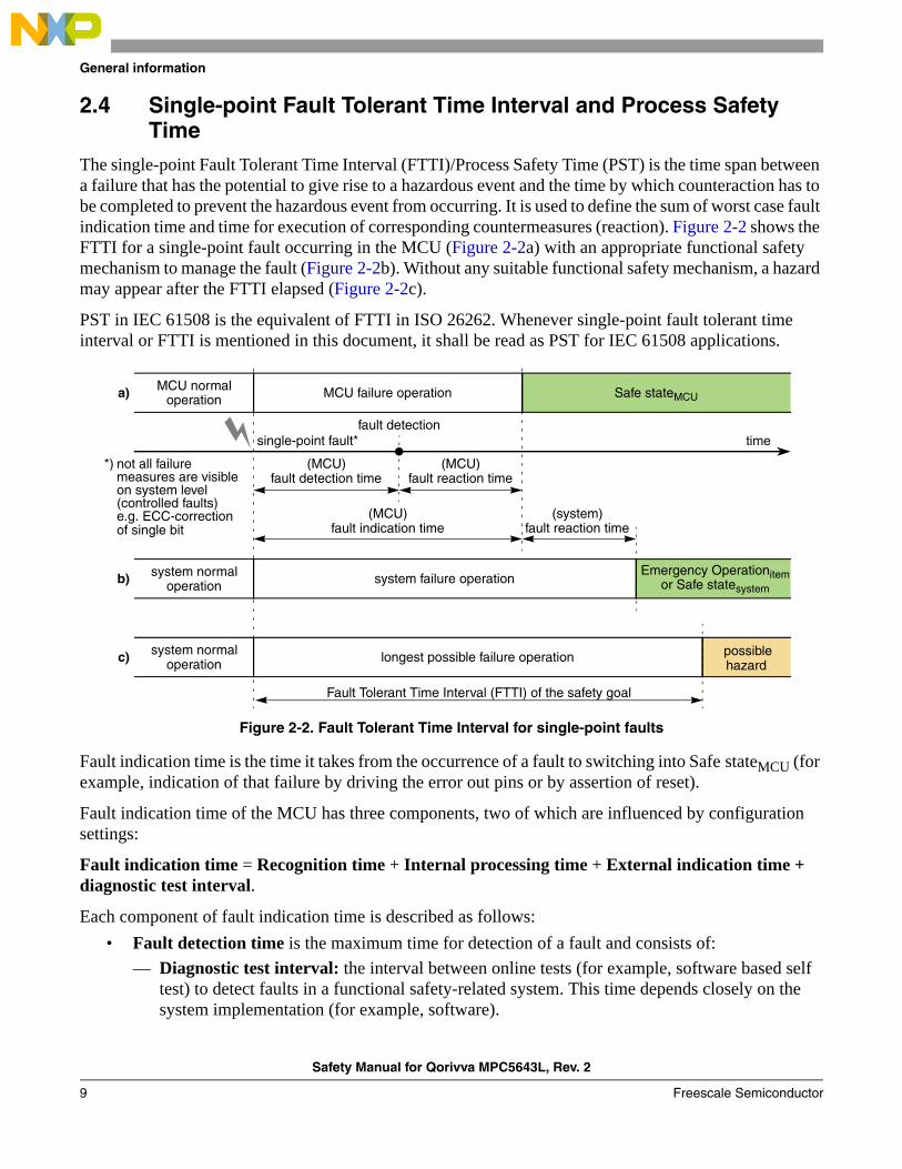
2.4 Single-point Fault Tolerant Time Interval and Process Safety Time
The single-point Fault Tolerant Time Interval (FTTI)/Process Safety Time (PST) is the time span between a failure that has the potential to give rise to a hazardous event and the time by which counteraction has to be completed to prevent the hazardous event from occurring. It is used to define the sum of worst case fault indication time and time for execution of corresponding countermeasures (reaction). Figure 2-2 shows the FTTI for a single-point fault occurring in the MCU (Figure 2-2a) with an appropriate functional safety mechanism to manage the fault (Figure 2-2b). Without any suitable functional safety mechanism, a hazard may appear after the FTTI elapsed (Figure 2-2c).
PST in IEC 61508 is the equivalent of FTTI in ISO 26262. Whenever single-point fault tolerant time interval or FTTI is mentioned in this document, it shall be read as PST for IEC 61508 applications.
Figure 2-2. Fault Tolerant Time Interval for single-point faults
Fault indication time is the time it takes from the occurrence of a fault to switching into Safe stateMCU (for example, indication of that failure by driving the error out pins or by assertion of reset).
Fault indication time of the MCU has three components, two of which are influenced by configuration settings:
Fault indication time = Recognition time + Internal processing time + External indication time + diagnostic test interval.
Each component of fault indication time is described as follows:
• Fault detection time is the maximum time for detection of a fault and consists of:
— Diagnostic test interval: the interval between online tests (for example, software based self test) to detect faults in a functional safety-related system. This time depends closely on the system implementation (for example, software).
Emergency Operationitemor Safe statesystem
Safe stateMCUMCU normal
operation MCU failure operation
(MCU)fault detection time
fault detection
(MCU)fault reaction time
(MCU)fault indication time
(system)fault reaction time
longest possible failure operation
system normaloperation system failure operation
system normaloperation
possible
time
b)
a)
c)
Fault Tolerant Time Interval (FTTI) of the safety goal
single-point fault*
*) not all failuremeasures are visibleon system level(controlled faults)e.g. ECC-correctionof single bit
hazard
Safety Manual for Qorivva MPC5643L, Rev. 2
Freescale Semiconductor9
General information
– Software cycle time of software based functional safety mechanisms. This time depends closely on the software implementation.
— Recognition time is the maximum of the recognition time of all involved functional safety mechanisms. The three mechanisms with the longest time are:
– ADC1 recognition time is a very demanding hardware test in terms of timing. The self-test requires the ADC conversion to complete a full test. A single full test takes at least 70 µs.2
– Recognition time related to the FMPLL loss of clock: it depends on how the FMPLL is configured. It is approximately 20 µs.
– Software execution time of software based functional safety mechanisms. This time depends closely on the software implementation.
• Fault reaction time is the maximum of the reaction time of all involved functional safety mechanisms consisting of internal processing time and external indication time:
— Internal processing time to communicate the fault to the FCCU lasts maximum 10 RC clock cycles (RC is the internal safe clock with nominal frequency of 16 MHz).
— External indication time to notify an observer about the failure external to the MCU. This time depends on the indication protocol configured in the Fault Collection and Control Unit (FCCU):
– Dual rail protocol and time switching protocol
— FCCU configured as “fast switching mode”: indication delay is a maximum of 64 µs. As soon as FCCU receives a fault signal, FCCU reports the failure to the system.
— FCCU configured as “slow switching mode”: an indication delay could occur. The maximum delay is equal to the period of the error out signal (FCCU_CFG.FOP). This parameter requires to be configured equal to its minimum which is 128 µs.
— Bi-stable protocol: indication delay is a maximum of 64 µs. As soon as the FCCU receives a fault signal, it reports the failure to the system.
If the configured reaction to a fault is an interrupt an additional delay (interrupt latency) can occur until the interrupt handler is able to start executing (for example, higher priority IRQs, XBAR contention, register saving, and so on).
The sum of the MCU fault indication time and system fault reaction time shall be less than the FTTI of the functional safety goal.
2.5 Latent Fault Tolerant Time Interval for latent faultsThe Latent Fault Tolerant Time Interval (L-FTTI) is the time span between a latent fault that has the potential to coincidently show up with other latent faults and give rise to a hazardous multiple-point event and the time by which counteraction has to be completed to prevent the hazardous event from occurring. It is used to define the sum of respective worst case fault indication time and time for execution of corresponding countermeasure. Figure 2-3 shows the L-FTTI for multiple-point faults in a system.
There is no equivalent to L-FTTI in IEC 61508.
1.ADC recognition time is relevant only if ADC is used by the safety function.2.This value takes into account the steps needed to run the three ADC hardware self-tests.
Safety Manual for Qorivva MPC5643L, Rev. 2
Freescale Semiconductor 10

General information
Figure 2-3. Fault Tolerant Time Interval for latent faults
Latent fault indication time is the time it takes from the occurrence of a multiple-point fault to when the indication of that failure is visible by driving the error out signals or by assertion of reset.
Fault indication time has three components, two of which are influenced by configuration settings:
Latent fault indication time = fault detection time + fault reaction time + diagnostic test interval.
Each component of fault indication time is described as follows:
• Fault detection time is the maximum of the detection time of all involved functional safety mechanisms. The mechanisms with the longest time are:
— Single bit corrected permanent hardware SRAM fault: this fault is only controlled (corrected); it is not reported (not detected) to the operator of the system. Therefore, it is a latent triple fault scenario, as ECC has a reduced capability to detect triple bit faults. The L-FTTI is in the range of 1×10⁹h-1 2×10⁵ years for a permanent single bit fault, or 20 years continuous operation for 10000 faults.
— Software execution time of software based functional safety mechanisms. This time depends closely on the software implementation.
For fault reaction time and diagnostic test interval, please refer to Section 2.4, Single-point Fault Tolerant Time Interval and Process Safety Time.
In general, fault reaction time and software execution time are negligible for multiple-point failures, as the L-FTTI is significantly larger than typical fault reaction time and software execution time.
Emergency Operationitemor Safe statesystem
Safe stateMCUMCU failure
(MCU)fault detection time
(MCU)fault indication time
longest possible failure operation
system failure operation
time
b)
a)
c)
Fault Tolerant Time Interval (FTTI)
latent fault*
*) fault not infringingthe safety for itself,only together withan additional fault(multiple fault)
operationMCU normal operation
system normal operation
**)probability of multiple point faultinfringing safety function is significante.g. 1/1000 of the total failure rate
of the safety goal multiple-point fault
detection interval ofthe safety goal
Fault Tolerant Time Interval (L-FTTI) of thesafety goal regarding Latent Faults
system normal operation
fault detection
(MCU)fault reaction time
multiple point fault**
possiblehazard
(system)fault reaction time
Safety Manual for Qorivva MPC5643L, Rev. 2
Freescale Semiconductor11
General information
The sum of the MPC5643L latent fault indication time and system multiple-point fault reaction time shall be less than the L-FTTI of the functional safety goal.
2.6 Failure handlingFailure handling can be split into two categories:
• Handling of failures before enabling the system level safety function (for example, during/following the MCU initialization). These errors are required to be handled before the system enables the safety function, or in a time shorter than the respective FTTI or L-FTTI after enabling the safety function.
• Handling of failures during runtime with repetitive supervision while the safety function is enabled. These errors are to be handled in a time shorter than the respective FTTI or L-FTTI.
Assumption: [SM_084] It is assumed that single-point and latent fault diagnostic measures complete operations (including fault reaction) in a time shorter than the respective FTTI or L-FTTI when the safety function is enabled.[end]
Recommendation: It is recommended to identify startup failures before enabling system level safety functions.
A typical failure reaction regarding power-up/start-up diagnostic measures is not to initialize and start the safety function and instead provide failure indication to the operator/user.
Safety Manual for Qorivva MPC5643L, Rev. 2
Freescale Semiconductor 12
Functional safety concept
3 Functional safety conceptFailures are the main impairment to functional safety:
• A systematic failure is manifested in a deterministic way to a certain cause (systematic fault) that can only be eliminated by a change of the design process, manufacturing process, operational procedures, documentation, or other relevant factors. Thus, measures against systematic faults are reduction of systematic faults: for example, implementing and following adequate processes.
• A random hardware failure can occur unpredictably during the lifetime of a hardware element; it follows a probability distribution. Thus, measures reducing the likelihood of random hardware faults include either the detection and control of faults during the lifetime of the hardware element, or a reduction of failure rates. A random hardware failure is caused by either a permanent fault (for example, physical damage), an intermittent fault, or a transient fault. Permanent faults are unrecoverable. Intermittent faults are, for example, faults linked to specific operating conditions or noise. Transient faults are, for example, particles (alpha, neutron) or EMI-radiation. An affected configuration register can be recovered by setting the desired value or by a power cycle. Due to a transient fault an element may be switched into a self destructive state (for example, single event latch up) and therefore may cause permanent destruction.
3.1 FaultsThe following random faults may generate failures, which may lead to the violation of a functional safety goal. Citations are according to ISO 26262-1. Random hardware faults occur at a random time, which results from one or more of the possible degradation mechanisms in the hardware.
• Single-Point Fault (SPF):An SPF is “a fault in an element that is not covered by a safety mechanism” and that results to a single-point failure “which leads directly to the violation of a safety goal.” Figure 3-4a shows an SPF inside an element, which generates a wrong output. The equivalent in IEC 61508 of a Single-Point Fault is a Random Fault. Whenever a SPF is mentioned in this document, it is to be read as a random fault for IEC 61508 applications.
• Latent Fault (LF):An LF is a “multiple-point fault whose presence is not detected by a safety mechanism nor perceived by the driver.” A LF is a fault that does not violate the functional safety goal(s) itself, but it leads, in combination with at least one additional independent fault, to a dual- or multiple-point failure, which then leads directly to the violation of a functional safety goal. Figure 3-4b shows an LF inside an element, which still generates a correct output. There is no IEC 61508 equivalent of LF.
• Residual Fault (RF):An RF is a “portion of a fault that by itself leads to the violation of a safety goal,” “where the portion of the fault is not covered by a functional safety mechanism.” Figure 3-4c shows an RF inside an element, which—although a functional safety mechanism is set in place—generates a wrong output, as this particular fault is not covered by the functional safety mechanism.
• Dual-point fault (DPF):A DPF is an “individual fault that, in combination with another independent fault, leads to a
Safety Manual for Qorivva MPC5643L, Rev. 2
Freescale Semiconductor13

Functional safety concept
dual-point failure” which leads directly to the violation to a goal. Figure 3-4d shows two LF inside an element, which generates a wrong output.
• Multiple-point fault (MPF):An MPF is an “individual fault that, in combination with other independent faults, leads to a multiple-point failure” which leads directly to the violation of a functional safety goal. Unless otherwise stated, multiple-point faults are considered as safe faults and are not covered in the functional safety concept of the MPC5643L.
• Safe Fault (SF):An SF is a “fault whose occurrence will not significantly increase the probability of violation of a safety goal.” Safe faults are not covered in this document. Single-point faults, residual faults, or dual-point faults are not safe faults.
Figure 3-4. Faults
SPFs shall be detected within the FTTI. Latent Faults (dual-point faults) shall be detected within the L-FTTI. In automotive applications, L-FTTI is generally accepted to be once per typical automotive trip time (Ttrip) by test routines (for example, BIST after power-up). This reduces the accumulation time of latent faults from life-time of the product Tlife to Ttrip.
Section 6.1, Mission profile lists a profile with a typical trip time for automotive applications and an alternative profile for continuous operation.
3.2 Failures• Common Cause Failure (CCF):
CCF is a coincidence of random failure states of two or more elements in separate channels of a redundancy element leading to the defined element failing to perform its intended safety function resulting from a single event or root cause (chance cause, non-assignable cause, noise, Natural pattern, …). Common Cause Failure causes the probability of multiple channels (N) having a failure rate to be larger than single channel
N (redundant element > single channelN).
SPFinput wrong
system
element
input
wrongoutput
system
element
RF safetymechanism
failureundetected
input correct
system
element
LF
input wrong
system
element
LFLF
a) Single-Point Fault (SPF)
c) Residual Fault (RF) d) Dual-Point Fault (DPF)
b) Latent Fault (LF)
output
output
output
Safety Manual for Qorivva MPC5643L, Rev. 2
Freescale Semiconductor 14

Functional safety concept
Figure 3-5. Common Cause Failures
• Common Mode Failure (CMF):CMF is a subset of CCF. A single root cause leads to similar coincidental erroneous behavior (with respect to the safety function) of two or more (not necessarily identical) elements in redundant channels, resulting in the inability to detect the failures. Figure 3-6 shows three elements within two redundant channels. One single root cause (CMF A or CMF B) leads to undetected failures in the primary channel and in one of the elements of the redundant channel.
Figure 3-6. Common Mode Failures
element
input failure b
channel 2
fault2
element
input failure a
channel 1
fault1
CCF
Remedial action
element
element
input
CMF A
output
comparison
secondary channel
primary channel
CMF B
failure
element
input
fault1
fault2 fault2’
fault1’
failure
Safety Manual for Qorivva MPC5643L, Rev. 2
Freescale Semiconductor15

Functional safety concept
• Cascading Failure (CF):CFs occur when local faults of an element in a system ripple through interconnected elements causing another element or elements of the same system and within the same channel to fail. Cascading Failures are dependent failures that are not Common Cause Failures. Figure 3-7 shows two elements within a single channel, to which a single root cause leads to a fault (fault 1) in one element resulting in a failure (failure a) causing a second fault (fault 2) within the second element (failure b).
Figure 3-7. Cascading Failures
element
inputfailure a
channel 1
fault1
element
failure bchannel 1
fault2
Safety Manual for Qorivva MPC5643L, Rev. 2
Freescale Semiconductor 16
Functional safety concept
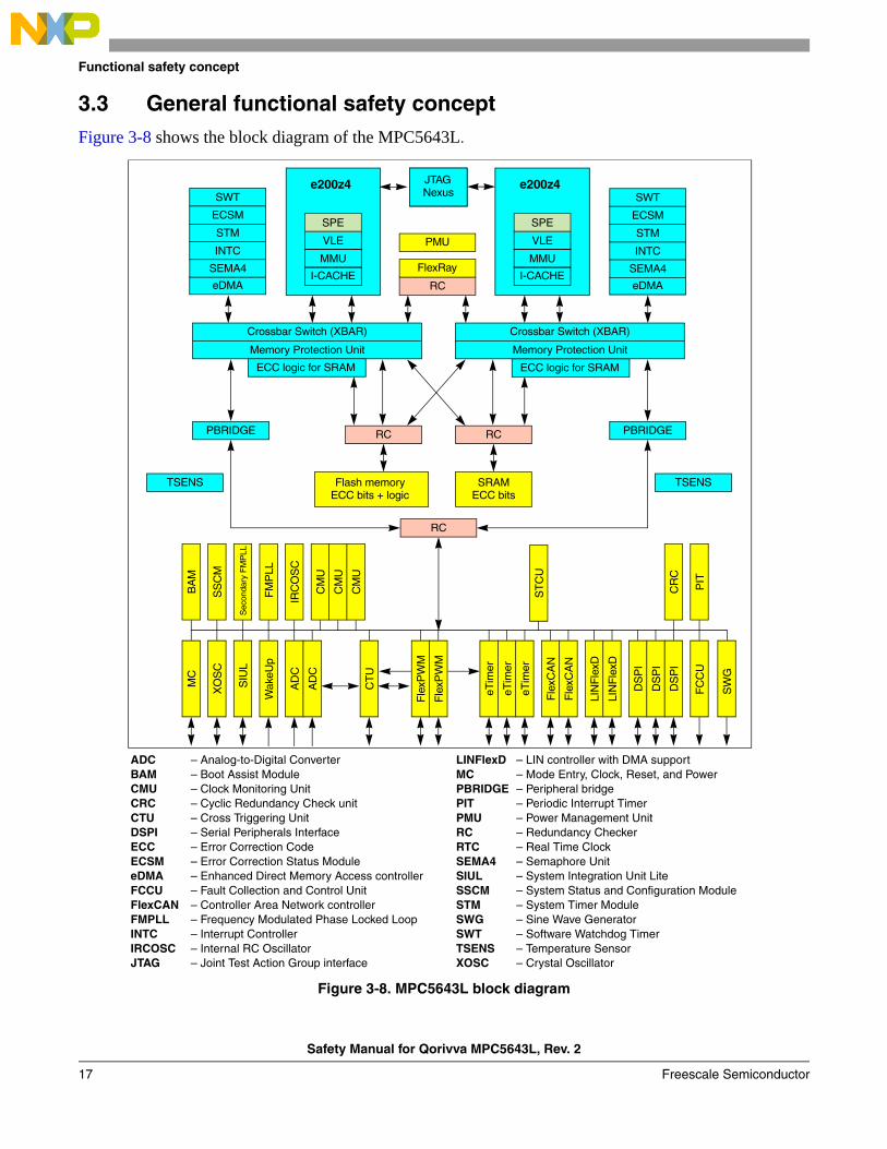
3.3 General functional safety conceptFigure 3-8 shows the block diagram of the MPC5643L.
Figure 3-8. MPC5643L block diagram
ADC – Analog-to-Digital ConverterBAM – Boot Assist ModuleCMU – Clock Monitoring UnitCRC – Cyclic Redundancy Check unitCTU – Cross Triggering UnitDSPI – Serial Peripherals InterfaceECC – Error Correction CodeECSM – Error Correction Status ModuleeDMA – Enhanced Direct Memory Access controllerFCCU – Fault Collection and Control UnitFlexCAN – Controller Area Network controllerFMPLL – Frequency Modulated Phase Locked LoopINTC – Interrupt ControllerIRCOSC – Internal RC OscillatorJTAG – Joint Test Action Group interface
LINFlexD – LIN controller with DMA supportMC – Mode Entry, Clock, Reset, and PowerPBRIDGE – Peripheral bridgePIT – Periodic Interrupt TimerPMU – Power Management UnitRC – Redundancy CheckerRTC – Real Time ClockSEMA4 – Semaphore UnitSIUL – System Integration Unit LiteSSCM – System Status and Configuration ModuleSTM – System Timer ModuleSWG – Sine Wave GeneratorSWT – Software Watchdog TimerTSENS – Temperature SensorXOSC – Crystal Oscillator
SRAM
SWT
ECSM
STM
INTC
eDMA
Crossbar Switch (XBAR)
VLE
MMU
I-CACHE
SPE
e200z4
VLE
MMU
I-CACHE
SPE
e200z4
Memory Protection Unit
Crossbar Switch (XBAR)
Memory Protection Unit
PBRIDGE
JTAGNexusJTAGNexus
RC
RC
RC
RC
FlexRay
PBRIDGE
TSENS TSENSECC bits
Flash memoryECC bits + logic
SIU
L
MC
Wak
eUp
AD
C
AD
C
XO
SC
BA
M
SS
CM
Sec
onda
ry F
MP
LL
FM
PLL
IRC
OS
C
CM
U
CM
U
CT
U
PIT
FC
CU
Fle
xPW
M
Fle
xPW
M
eTim
er
eTim
er
eTim
er
Fle
xCA
N
Fle
xCA
N
LIN
Fle
xD
LIN
Fle
xD
DS
PI
DS
PI
DS
PI
CR
C
CM
U
SEMA4
SWT
ECSM
STM
INTC
eDMA
SEMA4
SW
G
ECC logic for SRAM ECC logic for SRAM
ST
CU
PMU
Safety Manual for Qorivva MPC5643L, Rev. 2
Freescale Semiconductor17

Functional safety concept
Functional Safety integrity measures are as follows:
• Replication of IP: a dual core architecture reduces the need for component duplication at the system level, and lowers overall system level complexity.
• For the dual cores and their closely related periphery, functional safety is improved by a lockstep approach. Any deviation in the output of the two cores is detected by hardware and signaled as a possible failure.
• Error correction or detection, or both, for flash memory and SRAM to reduce the effect of transient faults and permanent faults in integrated volatile and non volatile memory.
• The generation and distribution of clock and power are supervised by dedicated monitors.
• Built-in self-tests (for example, MBIST and LBIST) are implemented in hardware to detect in general latent faults only and therefore reducing the risk of coincident latent faults (multiple-point faults).
• The Fault Collection and Control Unit (FCCU) is responsible for collecting and reacting to failure notifications.
• The Reset Generation Module (MC_RGM) replicates the reaction to failure notification for a set of critical failures.
• Risk of CMFs are reduced by a set of measures for both control and reduction of CMFs spanning system level approaches (such as temperature and non functional signal monitoring), physical separation, or diversity.
• The functional safety of the periphery is ensured by application-level (system-level) measures (such as connecting one sensor to different I/O modules, sensor validation by sensor fusion, etc.).
• Usage of internal (and external) watchdogs or timeout measures.
• Dedicated mechanisms are provided to check the functionality of each error reaction path (such as by application controlled fault injection).
Both cores can operate in either one of two distinct operating modes: Lockstep mode (LSM) or Decoupled Parallel mode (DPM). In DPM, the two channels of the MCU work independently. Automatic hardware checks for equal operation between the two channels are disabled in DPM. When in DPM, system level software measures are needed to achieve adequate functional safety integrity (for example, by implementing reciprocal comparisons).
The operating mode (LSM or DPM) on the MPC5643L is determined by the LSM_DPM user option bit in the shadow block of the flash memory, and is configured to the appropriate mode for the system level functional safety concept (see the “Selecting LSM or DPM” section of the “Operating Modes” chapter in the Qorivva MPC5643L Microcontroller Reference Manual).
As LSM is transparent to the system level (for example, to application software), specific requirements must be fulfilled to improve functional safety integrity in case the device is intended to operate in LSM (see Section 5.2.19, System Status and Configuration Module (SSCM)).
The MPC5643L microcontroller supports only static configuration at power-on (either LSM or DPM).
Assumption: [SM_091] For all information presented in this safety manual, it is assumed that the device operates in Lockstep mode (LSM). [end]
Safety Manual for Qorivva MPC5643L, Rev. 2
Freescale Semiconductor 18
Functional safety concept
3.3.1 Sphere of Replication—Lockstep mode (LSM)
The Sphere of Replication (SoR) contains all hardware elements that are replicated for functional safety reasons The replication is to detect permanent, dormant, latent, and transient faults. The following modules are included in the SoR:
• e200z4 core (including Memory Management Unit)
• Enhanced Direct Memory Access (eDMA)
• Interrupt Controller (INTC)
• Crossbar Switch (XBAR)
• Memory Protection Unit (MPU)
• Flash Memory Controller (PFlashC)
• Static RAM Controller (SRAMC)
• System Timer Module (STM)
• Software Watchdog Timer (SWT)
• Peripheral Bridge (PBRIDGE)
In LSM, each member of such a pair executes the same operations or transactions as its partner, resulting in lockstep behavior where both cores and their corresponding peripherals are in sync. The test for equal execution is checked on the boundary of the SoR by the redundancy Control Checker Units (RCCU).
Thus, the RCCUs implement a modified fault isolation in a way that they detect, but do not prevent, the propagation of a non-Common Mode Failure at the point where the two redundant channels are merged into a single actuator or recipient.
Isolation of the overall system is then achieved by the Fault Collection and Control Unit (FCCU) signaling an error, thereby allowing the device or application to react appropriately.
To simplify application software, the software executes transparently on both cores of the MPC5643L and the application sees only one logical core.
Safety Manual for Qorivva MPC5643L, Rev. 2
Freescale Semiconductor19

System-level hardware requirements
4 System-level hardware requirementsThis section lists necessary or recommended measures on the system level for the MPC5643L to achieve the functional safety goal(s).
The MPC5643L offers an integrated functional safety architecture using dual-core lockstep CPU (LSM), a variety of replicated function blocks, several self-test units, and other elements to detect faults. By these means, SPFs and LFs can be detected with a high diagnostic coverage. However, not all Common Mode Failures may be detected. To detect failures, which may not be detected by the MPC5643L itself, it is assumed that a separate device is used to bring the system into Safe statesystem in such cases.
Figure 4-9 depicts a simplified application schematic for a functional safety relevant application in conjunction with a separate IC (only functional safety-related elements shown). The MPC5643L is supplied with its required supply voltages (1.2 V, 3.3 V and opt. 5 V). Although for most applications the 1.2 V for digital core supply is generated by an external ballast transistor from 3.3 V supply, internal ballast transistor of the MPC5643L can be used as well. Voltages generated within the separate IC need to be monitored for over voltage (over voltage supervision).
The separate integrated circuit also monitors the state of the error out signals FCCU_F[n] (error monitor). Through a communication interface (for example, SPI), the MPC5643L repetitively triggers the watchdog of the separate IC. In case of a failure (if the watchdog is not serviced correctly, for example), reset output is asserted LOW to reset the MPC5643L. A fail-safe output is available to control or deactivate any fail-safe circuitry (for example, a power switch).
Figure 4-9. Functional safety-related connection to a separate device
4.1 Assumed functions by separate deviceThis section describes separate components supporting the usage of the MPC5643L for applications requiring high functional safety integrity levels.
BCTRL
3.3VVDD_HV
3.3V/5VVDD_LV
VDD_HV_ADR
RESET
FCCU_F[0](FCCU_F[1])
SPI (or alternative)
External IC
over voltagesupervision
errormonitor
watchdog
Fail safe output(e.g. power switch)
1.2V
MPC5643L
(optional)
Safety Manual for Qorivva MPC5643L, Rev. 2
Freescale Semiconductor 20

System-level hardware requirements
Failure rates of external services are only included for specific circuitries (clock, 1.2 V supply) in the FMEDA of the MPC5643L and have to be included in the system FMEDA by the system integrator.
4.1.1 High-impedance outputs
Assumption under certain preconditions: [SM_074] If an output in high-impedance is not considered safe at system level, it is assumed that countermeasures are placed to bring the safety-critical outputs to their Safe state.[end]
Rationale: To bring the functional safety-critical outputs to such a level, that a Safe statesystem is achieved.
Implementation hint: If the Safe stateMCU “Completely unpowered” and “No active output (tristate)” is not compliant to system level Safe statesystem, a possible system-level countermeasure may be to place pull-up or pull-down resistors to match the two sets of Safe states.
4.1.2 External Watchdog (EXWD)
A simple separate device, acting as supervisor of the operations, should be used as watchdog as described in Section 7.3.2, External timeout function.
Assumption: [SM_075] It is assumed that correct operation of the MPC5643L is supervised by a separate device. This device moves the system to a Safe statesystem when it detects incorrect operation of MPC5643L.[end]
Recommendation: It is recommended to use an external watchdog which is triggered periodically by the safety relevant software running on the MPC5643L.
Rationale: To cover situations when MPC5643L is not able to signal a failure.
Note: There must be a signalling path from the functional safety software to the external system through which the software can confirm the correct initialization. This is not automatically guaranteed by the FCCU_F[n] signals, which communicate the status of the device which is independent from software. On the other hand, a different communications interface (such as a serial link) can be used to detect incorrect software initialization.
If a failure is detected, the external watchdog (EXWD) switches the system to a Safe statesystem within the FTTI.
The timeout (watchdog) may be triggered periodically by the MPC5643L within the functional safety relevant software. The trigger may be discrete signal(s) or message object(s). If within a timeout period not triggered, a failure is detected by the external timeout (watchdog) function which switches the whole system to a Safe statesystem within the FTTI (for example, the EXWD disconnects MPC5643L from the power supply, or the communication messages are invalidated by disabling the physical layer driver).
The implementation of the communication between the MPC5643L and the separate device can be chosen as desired. The timeout (watchdog) can be triggered, for example, by communication via:
• Serial link (SPI)
• Toggling I/O (GPIO)
• Periodic message frames (FlexCAN, FlexRay)
Safety Manual for Qorivva MPC5643L, Rev. 2
Freescale Semiconductor21

System-level hardware requirements
• Toggling FCCU_F[0], FCCU_F[1] error out signals from the FCCU
4.1.3 Power Supply Monitor (PSM)
Supply voltage above the specified operational range might cause permanent damage to the MPC5643L even if kept in reset. Therefore, it is either required in case of over voltage to de-energize the MPC5643L or to decommission/replace the MPC5643L after an over voltage event.
For the specified operating voltage range, please refer to MPC5643L, Qorivva MPC5643L Microcontroller Data Sheet.
Assumption: [SM_076] It is assumed that measures on the system level maintain the Safe statesystem during and after any supply voltage above the specified operational range.[end]
Recommendation: It is recommended on the system level to avoid over voltage supply to the MPC5643L or to permanently disable (Safe statesystem) in case of an over voltage.
Rationale: To ensure operation according to data sheet.
Implementation hint: A separate and independent device may provide an over voltage monitor for the MPC5643L external 3.3 V supplies. If the power supply is above the recommended operating voltage range of the MPC5643L, the MPC5643L is to be kept powerless and the power supply monitor switches the system to a Safe statesystem within the FTTI and maintains it in Safe statesystem (over voltage protection with functional safety shut-off or a switch-over to a second power supply unit).
In cases where over voltages can be completely inhibited by the power supply design, over voltage monitoring is dispensable.
Over voltage on the1.2 V core supply may be detected by the MPC5643L itself. But system level measure may be required to maintain the Safe statesystem in case an over voltage cause destructive damages within the MCU.
4.1.4 Error Out Monitor (ERRM)
If the MPC5643L signals an internal failure via its error out signals (FCCU_F[0] and optionally FCCU_F[1]), the system cannot rely on the integrity of the MPC5643L outputs (other than FCCU_F[0] and FCCU_F[1]) for safety functions. If an error out is indicated, the system must transition to and remain in Safe statesystem. Depending on its functionality, the system might disable or reset the device as a reaction to the indicated error out (see the assumptions in Section 2.3, Safe state).
The system integrator can choose between two different methods to interface to the FCCU:
• Both FCCU signals connected to the separate device
• Only a single FCCU signal connected to the separate device
Both FCCU configurations work properly with all the supported error out protocols. Refer to the Qorivva MPC5643L Microcontroller Reference Manual for a list of supported protocols.
Recommendation: It is recommended to correctly configure the FCCU to report detected critical failures via FCCU_F[0] and optionally FCCU_F[1] to fulfill the system level requirements regarding FTTI.
Safety Manual for Qorivva MPC5643L, Rev. 2
Freescale Semiconductor 22

System-level hardware requirements
Rationale: To monitor the error out signals for correct functionality of the device.
4.1.4.1 Both FCCU signals connected to separate device
In this configuration, the separate device continuously monitors the output of the FCCU. Thus, it can detect if the FCCU does not work properly.
This configuration may not require any dedicated software support.
Assumption under certain preconditions: [SM_079] If both error out signals (FCCU_F[0] and FCCU_F[1]) are connected to a separate device, it is assumed that the separate device checks both signals, taking into account that FCCU_F[0] = FCCU_F[1].[end]
Rationale: To check the integrity of the FCCU and FCCU signal routing on the system level.
Monitoring the error output signals through an asynchronous combinatorial logic (for example, XOR gate) can generate some glitches. Synchronous sampling or asynchronous oversampling these signals reduces the likelihood of glitches.
4.1.4.2 Single FCCU signal connected to separate device
A single signal, FCCU_F[0] (or FCCU_F[1]), is connected to the separate device.
If a fault occurs, the FCCU communicates it to the separate device through the FCCU_F[0] (or FCCU_F[1]) signal.
The functionality of FCCU_F[0] (or FCCU_F[1]) can at least be checked in the following manner:
• FCCU_F[0] (or FCCU_F[1]) output read back (internal connection)
• FCCU_F[0] (or FCCU_F[1]) output connected externally to a normal GPIO.
• FCCU_F[0] (or FCCU_F[1]) checked by separate device.
The system integrator is asked to choose which solution fits the system level functional safety requirement.
The advantage of a single FCCU_F[n] signal being used instead of using both FCCU_F[n] signals as in the previous section, is the lack of necessity for a separate device to be used for comparing the FCCU_F[n] signals.
Assumption under certain preconditions: [SM_080] If a single signal, FCCU_F[0] or FCCU_F[1], is connected to a separate device, it is assumed that the correct operation of this signal is checked before executing any safety function.[end]
Rationale: To check the integrity of the FCCU error out I/O.
To verify the functionality of an FCCU_F[n] signal, a fault may be injected and the behavior of the pin may be checked by the other error out signal, GPIO, or separate device. It is possible to change the polarity of the error out signal by configuring the FCCU_CFG[FCCU_CFG.PS] bit. Other methods for checking the functionality of FCCU_F[0] (or FCCU_F[1]) may be implemented.
Because FCCU is monitoring the system, it is sufficient to check FCCU_F[0] (or FCCU_F[1]) within the L-FTTI (for example, at power-up) to reduce the risks of latent faults. It is recommended that FCCU_F[n] be checked once before the system begins performing the safety relevant function.
Safety Manual for Qorivva MPC5643L, Rev. 2
Freescale Semiconductor23

System-level hardware requirements
If the system is using the MPC5643L in a single error output signal mode, the application software configures the signals and pads neighboring the FCCU_F[0] (or FCCU_F[1]) to use a lower drive strength.
Using a lower drive strength on the GPIO near FCCU_F[0] (or FCCU_F[1]) will result in the higher current strength of FCCU_F[n] to affect the logic level of the neighboring GPIO in the event of a short circuit. Software may configure the slew rate for the relevant GPIO in the Pad Configuration Register (PCR).
4.2 Optional hardware measures on system levelAs I/O operations are highly application dependant, functional safety assessments are not effective on the MPC5643L level. Functional safety of I/O modules and peripherals may be assessed on a system level. The following sections provide examples of possible functional safety mechanisms regarding some I/O operations.
4.2.1 PWM output monitor (PWMA)
Assumption under certain preconditions: [SM_083] When FlexPWM outputs are used in the implementation of a safety function with specific requirements, suitable system level functional safety integrity measures are assumed to monitor these signals.[end]
Recommendation: System level measures to detect or avoid erroneous PWM output signals are recommended to improve the safety integrity of PWM channels.
Monitoring can be implemented explicitly by monitoring the PWM signal directly with a separate device. An alternative approach implicitly monitors the PWM signal by implementing an indirect PWM feedback loop, for example, measuring average current flow of full bridge driver. This approach may use diverse implemented input modules (for example, the analog-to-digital converte)r.
The distinctive PWM features that are to be managed by the system level measures are:
• Dead-time may need to be always positive and greater than the maximum value between TON and TOFF of the inverter switches.
• Open GPIO and short to supply or ground may need to be detected. This can be detected, for example, by an MCU external feedback loop to a timer module of the MPC5643L capable of performing input capture functionality (for example, eTimer).
The system must be switched to Safe statesystem if the MPC5643L detects an error.
To reduce the likelihood of erroneous control (for example, a motor control application with dead-time requirements to reduce the likelihood of short circuits destroying the motor) in functional safety applications using I/O to control an actuator with short FTTI, the functional safety requires system level supervision if the maximum fault indication time and fault reaction time of the MPC5643L exceed the FTTI of the actuators.
If the PWM signals drive switches of a power stage (for example, a bridge driver), the eTimer may not be fast enough to detect a dead-time fault because its fault indication time is often greater than the time required to avoid destruction of the power stage.
Safety Manual for Qorivva MPC5643L, Rev. 2
Freescale Semiconductor 24

System-level hardware requirements
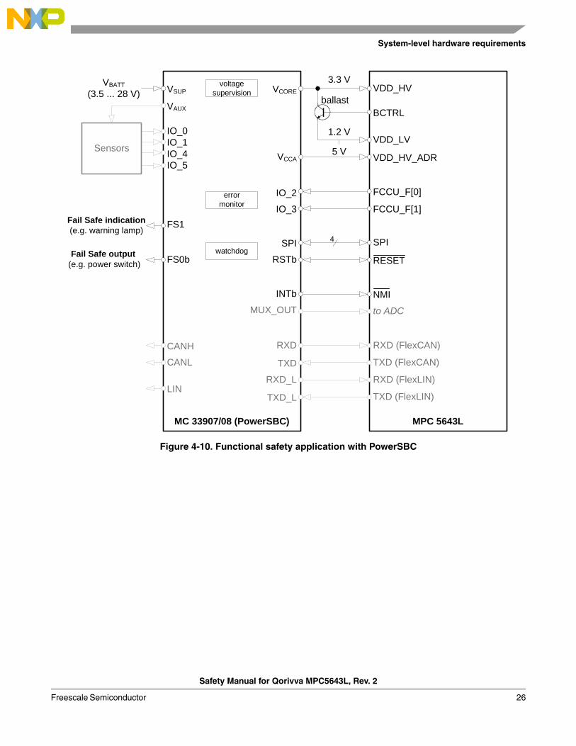
4.3 PowerSBCThe system basis chips MC33907 and MC33908 (PowerSBC) from Freescale are ideally suited to be used in combination with MPC5643L to serve as a separate device as mentioned in Section 4.1, Assumed functions by separate device.
The MC33907/08 is a multi-output power supply integrated circuit including enhanced functional safety features dedicated to the automotive market. It has been developed in accordance with ISO 26262.
Figure 4-10 depicts a simplified application schematic for a functional safety relevant application in conjunction with MPC5643L.
Out of a single battery supply with a wide voltage range (VSUP, 3.5 V…28 V), the MC33907/08 generates 5 V (VCCA) and 3.3 V (VCORE) to supply the MPC5643L as well as an auxiliary voltage (VAUX) to supply other devices (for example, sensors or separate ICs). The 1.2 V for digital core supply is generated by an external ballast transistor from VCORE. All voltages generated in the MC33907/08 are independently monitored for under and over voltage.
The MC 33907/08 also monitors (monitoring pins IO_2, IO_3) the state of the error out pins FCCU_F[0] and FCCU_F[1], using the bi-stable protocol. Via SPI, the MPC5643L repetitively triggers the windowed watchdog of the MC33907/08 with a valid answer. A dedicated fail safe state machine is implemented to bring and maintain the application in Safe stateitem. In case of a failure (for example, the watchdog is not serviced correctly), RSTb is asserted LOW to reset the MPC5643L. A fail-safe output (FS0b) is available to control or deactivate any fail-safe circuitry (a power switch, for example). Another fail-safe output is available with PWM-encoding for error indication (a warning lamp, for example). MC 33907/08 includes built-in self-tests.
An interrupt output (INTb) for error information is connected to the NMI input of the MPC5643L.
By a connection of the signal MUX_OUT to an ADC-input of MPC5643L, further diagnostic measures are possible (for example, reading temperature or measuring VBATT). Digital inputs (IO_0, IO_1, IO_4, IO_5) may be used for monitoring error signal handling of other devices. Additionally, MC33907/08 may act as a physical interface to connect the MPC5643L directly with a CAN or LIN bus.
Safety Manual for Qorivva MPC5643L, Rev. 2
Freescale Semiconductor25
System-level hardware requirements
Figure 4-10. Functional safety application with PowerSBC
MC 33907/08 (PowerSBC) MPC 5643L
VDD_HV
VDD_HV_ADR
FCCU_F[0]
SPI
RSTb
FCCU_F[1]
IO_2
IO_3
SPI
VCORE
VCCA
FS0b
FS1
Fail Safe output (e.g. power switch)
Fail Safe indication (e.g. warning lamp)
VDD_LV
BCTRL
voltagesupervision
errormonitor
watchdog
INTb
MUX_OUT to ADC
5 V
1.2 V
3.3 V
RESET
Sensors
IO_0IO_1IO_4IO_5
VAUX
VSUPVBATT
(3.5 ... 28 V)
RXD (FlexCAN)
TXD (FlexCAN)
RXD (FlexLIN)
TXD (FlexLIN)
RXD
TXD
RXD_L
TXD_L
CANH
CANL
LIN
4
NMI
ballast
Safety Manual for Qorivva MPC5643L, Rev. 2
Freescale Semiconductor 26

System-level software requirements
5 System-level software requirementsThis section lists required or recommended measures when using the individual components of the MPC5643L.
Before executing any safety function, it is assumed that the conditions described in the sections “Initial checks and configurations” of some modules are satisfied by application software.
During the execution of the safety function, application software is assumed to perform a set of runtime tasks, described in the “Runtime checks” sections of some modules, to support the detection of random hardware failures and transition the device to a Safe stateMCU in case of a failure.
Given the application independent nature of the MPC5643L, no general safety function can be specified. To define a specific safety function, the MPC5643L would have to be integrated into a complete (application dependent) system. Nevertheless, it is possible to define abstract element safety functions and safety integrity functions:
• An element safety function is used to implement (or control) a functional safety means with available hardware
• A safety integrity function (often reductively called diagnostic measures) is to improve the probability of successful execution of a functional safety means
It is nevertheless possible to ignore the required measures if equivalent measures to manage the same failures are included instead.
The modules covered by the SoR reach a very high diagnostic coverage (DC) without additional dedicated measures at application or system level.
5.1 Disabled modes of operationThe system level and application software must ensure that the functions described in this section are not activated while running functional safety-relevant operations.
5.1.1 Debug mode
The debugging facilities of the MCU pose a possible source of failures in case they activate during the operation of functional safety-relevant applications. They can halt the cores, cause breakpoints to hit, write to core registers and the address space, and activate boundary scan. The MCU may not enter debug mode to reduce the likelihood of interference with the normal operation of the application software. The state of the JCOMP signal determines whether the system is being debugged or whether the system operates in normal operating mode. When JCOMP is logic low, the JTAGC TAP controller is kept in reset for normal operating mode. When it is logic high, the JTAGC TAP controller is enabled to enter debug mode. On the system level, measures must be taken to ensure that JCOMP is not be asserted by external sources to avoid entering debug mode. The activation of debug mode is supervised by the FCCU, and it signals a fault condition when debug mode is entered.
Safety Manual for Qorivva MPC5643L, Rev. 2
Freescale Semiconductor27

System-level software requirements
5.1.2 Test mode
Several mechanisms of the MCU can be circumvented in test mode which endangers the functional safety integrity.
It is assumed that the device is not operated in test mode. Test mode is used for comprehensive factory testing and is not validated for normal operational usage.
Implementation hint: The VPP_TEST pin is for testing purposes only, and must be tied to GND in normal operating mode. From a system level point of view, measures must ensure that the VPP_TEST pin is not asserted to VDD during boot to avoid entering test mode. The activation of test mode is supervised by the FCCU and it signals a fault condition when test mode is entered.
5.2 MPC5643L modules
5.2.1 Fault Collection and Control Unit (FCCU)
The FCCU offers a hardware fail safe channel to collect faults and to bring the device into a Safe stateMCU when a failure has occurred.
All faults detected by hardware measures are reported to the central Fault Collection and Control Unit (FCCU). It monitors critical control signals and collects all errors. Depending on the particular fault, the FCCU puts the device into the accordingly configured Safe stateMCU. This prevents fault propagation (cascading faults) to system level. Only hardware configuration of the FCCU may be required by application software. No CPU intervention is required for collection and control operation.
The FCCU offers a systematic approach to fault collection and control. It is possible to configure the reaction for each fault source separately. The distinctive features of the module are:
• Collection of redundant hardware checker results (for example, the RCCU. See Section 5.2.6, Redundancy Control Checking Unit (RCCU))
• Collection of error information from modules whose behavior is essential with respect to the functional safety goal
• Configurable and graded fault control:
— Internal reactions
– No reset reaction
– IRQ
– Functional reset
– MPC5643L safe mode entered
— External reaction (failure is reported to the outside world via output signal(s) FCCU_F[n])
Two classes of faults are identified based on the criticality and the related reactions:
• Critical faults
• Non-critical faults
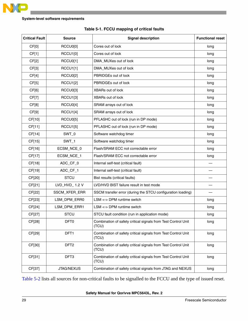
Table 5-1 lists sources for critical faults to be signalled to the FCCU and the type of issued reset.
Safety Manual for Qorivva MPC5643L, Rev. 2
Freescale Semiconductor 28
System-level software requirements
Table 5-2 lists all sources for non-critical faults to be signalled to the FCCU and the type of issued reset.
Table 5-1. FCCU mapping of critical faults
Critical Fault Source Signal description Functional reset
CF[0] RCCU0[0] Cores out of lock long
CF[1] RCCU1[0] Cores out of lock long
CF[2] RCCU0[1] DMA_MUXes out of lock long
CF[3] RCCU1[1] DMA_MUXes out of lock long
CF[4] RCCU0[2] PBRIDGEs out of lock long
CF[5] RCCU1[2] PBRIDGEs out of lock long
CF[6] RCCU0[3] XBARs out of lock long
CF[7] RCCU1[3] XBARs out of lock long
CF[8] RCCU0[4] SRAM arrays out of lock long
CF[9] RCCU1[4] SRAM arrays out of lock long
CF[10] RCCU0[5] PFLASHC out of lock (run in DP mode) long
CF[11] RCCU1[5] PFLASHC out of lock (run in DP mode) long
CF[14] SWT_0 Software watchdog timer long
CF[15] SWT_1 Software watchdog timer long
CF[16] ECSM_NCE_0 Flash/SRAM ECC not correctable error long
CF[17] ECSM_NCE_1 Flash/SRAM ECC not correctable error long
CF[18] ADC_CF_0 Internal self-test (critical fault) —
CF[19] ADC_CF_1 Internal self-test (critical fault) —
CF[20] STCU Bist results (critical faults) —
CF[21] LVD_HVD_ 1.2 V LVD/HVD BIST failure result in test mode —
CF[22] SSCM_XFER_ERR SSCM transfer error (during the STCU configuration loading) —
CF[23] LSM_DPM_ERR0 LSM <-> DPM runtime switch long
CF[24] LSM_DPM_ERR1 LSM <-> DPM runtime switch long
CF[27] STCU STCU fault condition (run in application mode) long
CF[28] DFT0 Combination of safety critical signals from Test Control Unit (TCU)
long
CF[29] DFT1 Combination of safety critical signals from Test Control Unit (TCU)
long
CF[30] DFT2 Combination of safety critical signals from Test Control Unit (TCU)
long
CF[31] DFT3 Combination of safety critical signals from Test Control Unit (TCU)
long
CF[37] JTAG/NEXUS Combination of safety critical signals from JTAG and NEXUS long
Safety Manual for Qorivva MPC5643L, Rev. 2
Freescale Semiconductor29

System-level software requirements
The FCCU has two external signals, FCCU_F[0] and FCCU_F[1]. Critical errors are reported on these signals. When the device is in reset or unpowered, these outputs are three-stated.
FCCU_F[n] are intended to be connected to an independent device which continuously monitors these signals. If a failure is detected, the separate device switches to and maintains the system to a Safe statesystem condition within the FTTI (for example, the separate device disconnects the MPC5643L device from the power supply).
Table 5-2. FCCU mapping of noncritical faults
Non-critical fault
Source Signal description Functional reset
NCF[0] Core_0 watchdog p_wrs_core0[0] long
NCF[1] Core_1 watchdog p_wrs_core1[0] long
NCF[2] FM_PLL_0 Loss of lock long
NCF[3] FM_PLL_1 Loss of lock long
NCF[4] CMU_0 Loss of XOSC clock long
NCF[5] CMU_0 System clock (Sysclk) frequency out of range long
NCF[6] CMU_1 Motor control clock (MOTC_CLK) frequency out of range long
NCF[7] CMU_2 FlexRay clock (FRPE_CLK) frequency out of range long
NCF[8] ECSM_ECN_0 ECC 1-bit error correction notification —
NCF[9] ECSM_ECN_1 ECC 1-bit error correction notification —
NCF[10] ADC_NCF_0 Internal self-test (non critical fault) —
NCF[11] ADC_NCF_1 Internal self-test (non critical fault) —
NCF[12] STCU_NCF Bist results (non critical faults) —
NCF[13] LVD_ 1.2 V LVD BIST OK in test mode/ LVD NOK in user mode —
NCF[14] HVD_ 1.2 V HVD BIST OK in test mode/ HVD NOK in user mode —
NCF[15] LVD VREG LVD VREG fault detected by self-checking —
NCF[16] LVD FLASH LVD FLASH fault detected by self-checking —
NCF[17] LVD IO LVD IO fault detected by self-checking —
NCF[19] FLEXR_ECN ECC 1-bit error correction notification from flexray —
NCF[20] FLEXR_NCE ECC not correctable error from flexray (combination of LRAM and DRAM ECC errors)
—
NCF[21] MC_ME Software device reset —
NCF[22] BP_BALLAST0 Bypass Ballast0 —
NCF[23] BP_BALLAST1 Bypass Ballast1 —
NCF[24] BP_BALLAST2 Bypass Ballast2 —
Safety Manual for Qorivva MPC5643L, Rev. 2
Freescale Semiconductor 30
System-level software requirements
5.2.1.1 Initial checks and configurations
Besides the possible initial configuration, no CPU intervention is necessary for fault collection and fault reaction.
Assumption: [SM_073] It is assumed that all reactions of the FCCU related to faults of peripherals used by the system level safety function are enabled.[end]
Rationale: Maintain the device in the Safe statesystem in case of failure.
Implementation hint: The FCCU fault path is enabled by configuring FCCU registers (for example, FCCU_CF_CFG0, FCCU_NCF_CFG0, FCCU_CFS_CFG0, FCCU_NCFS_CFG0, FCCU_NCF_TOE0, and so on).
When a Clock Monitoring Unit (CMU) monitors a FMPLL that is not used, or is not used for functional safety critical modules, error masking and limited internal reaction can be tolerated.
Only functional resets, or a switch to a Safe stateMCU, are appropriate as internal reactions.
External reaction of the FCCU is always enabled and can not be disabled.
If the MPC5643L signals an internal failure via its error out signals (FCCU_F[0:1]), the system can no longer trust the MPC5643L outputs used within the safety function. If an error is indicated, the system has to be able to remain in Safe statesystem without any additional action from the MPC5643L. Depending on its functionality, the system might disable or reset the MPC5643L as a reaction to the indicated error out.
5.2.1.2 Runtime checks
Assumption under certain preconditions: [SM_001] If the continuous switching of MPC5643L between a standard operation state and the reset state or Fault State without any device shutdown does not meet the Safe statesystem, it is assumed that system level measures are implemented to prevent continuous switching.[end]
Recommendation: It is recommended that the application identifies and signals such switching as a failure condition.
Rationale: The system is not considered to be in a Safe statesystem when continuously switching.
Implementation hint: Software may be implemented to reduce the likelihood of cycling between a functional and a fault state. For example, in case of periodic noncritical faults, the software could clean the respective status and periodically move the device from fault state to normal state. This looping may be avoided.
Assumption under certain preconditions: [SM_082] If the continuous switching of MPC5643L between a standard operation state and the reset state or Fault State without any device shutdown does not meet the Safe statesystem, it is assumed that software keeps track of cleaned faults, stops cleaning, and stays in a Safe stateMCU instead in case of inacceptable high frequency of necessary fault cleaning.[end]
Rationale: To prevent permanent cycling between a functional state and a fault state.
Safety Manual for Qorivva MPC5643L, Rev. 2
Freescale Semiconductor31

System-level software requirements
The limit for the number and frequency of clearances is application dependent. This may only be relevant in case continuous switching between a standard operation state and reset state as a failure condition is not a Safe statesystem.
5.2.2 Reset Generation Module (MC_RGM)
A redundant fault notification path is achieved through the use of the Reset Generation Module (MC_RGM) and the Fault Collection and Control Unit (FCCU).
Detected critical errors are forwarded independently to the Reset Generation Module (MC_RGM) and Fault Collection and Control Unit (FCCU). Additionally, the state of the MC_RGM is forwarded to the FCCU and the FCCU forwards an additional reset request to the MC_RGM. This decreases the likelihood of Common Mode Failures on the functional safety path and it ensures reaction to failures in all cases. Even if FCCU were to fail, a reset would be generated by MC_RGM to enter Safe stateMCU.
5.2.2.1 Initial checks and configurations
Assumption: [SM_007] It is assumed that a second failure notification channel is configured to communicate critical application faults redundantly.[end]
Recommendation: It is recommended to configure both MC_RGM and FCCU to react to critical application faults.
Rationale: To have two notification paths in case of an error.
Implementation hint: To enable critical events to trigger a reset sequence, MC_RGM_FERD is set to 0. If particular events are excluded, MC_RGM_FEAR is configured to generate an alternate request in these cases.
To trigger a reset of the device by software, the MC_ME_MCTL[TARGET_MODE] may be used. Writing MC_ME_MCTL[TARGET_MODE] = 0000b causes a functional reset, and writing MC_ME_MCTL[TARGET_MODE] = 1111b causes a destructive reset.
5.2.3 Self Test Control Unit (STCU)
The STCU executes built-in self-tests (LBIST, MBIST) and gives reaction to detected faults by triggering a Noncritical Fault (NCF) to the FCCU (see the “Self-Test Control Unit (STCU)” chapter of the Qorivva MPC5643L Microcontroller Reference Manual for details).
5.2.3.1 Initial checks and configurations
Assumption: [SM_092] It is assumed that LBISTs and MBISTs are executed once per trip time.[end]
The STCU does not require any configuration performed by application software.
Assumption: [SM_006] It is assumed that correct behavior of the STCU is checked before executing a safety function.[end]
Recommendation: It is recommended to confirm that all MBISTs and LBISTs finished successfully with no additional errors flagged.
Safety Manual for Qorivva MPC5643L, Rev. 2
Freescale Semiconductor 32

System-level software requirements
Rationale: The STCU’s correct behavior has to be verified by checking the expected results with software.
Implementation hint: System (application) level software may carry out checking of STCU for ensuring STCU integrity. See the “Integrity SW Operations” section of the “Self-Test Control Unit (STCU)” chapter in the Qorivva MPC5643L Microcontroller Reference Manual for details.
This software confirmation prevents a fault within the STCU itself from incorrectly indicating that the built-in self-test passed.
This is an additional functional safety layer because the STCU propagates the LBIST/MBIST and internal faults using the CF signals of the FCCU. So, reading STCU_LBS, STCU_LBE, STCU_MBSL, STCU_MBSH, STCU_MBEL, STCU_MBEH, and STCU_ERR registers helps to increase the STCU auto-test coverage.
5.2.4 Temperature Sensor (TSENS)
Two temperature sensors monitor the substrate temperature to detect over-temperature conditions before they cause a Common Mode Failure (for example, faults due to over-temperature causing identical erroneous results from both cores). The maximum operating junction temperature is specified in the device data sheet. The two outputs, one for each instance, are forwarded to the two analog acquisition channels for measurement (temperature sensor 0 mapped to channel 15 of ADC_0 and temperature sensor 1 mapped to channel 15 of ADC_1) to maximize the independence of the temperature information. The measured temperatures may also be compared to each other to detect possible malfunctions of the sensors themselves.
To reduce the likelihood of Common Mode Failure(s), the effects of increasing temperature, for example, due to random hardware fault(s) may be controlled on the system level.
The potential for over-temperature operating conditions needs to be reduced by appropriate system level measures. Possible measures include:
• Actuation of the functional safety shut-off via thermal fuse
• Several levels of over-temperature sensing and alarm triggering
• Connection of forced-air cooling and status indication
5.2.4.1 Initial checks and configurations
Assumption under certain preconditions: [SM_059] If a temperature sensor is used in a safety function, it is assumed that the two temperature sensors are read during power-up and that the read values are confirmed to be similar.[end]
Rationale: To assess functionality of the temperature sensors.
However, nothing prohibits reading the temperature sensors during execution of the safety function (application runtime).
Safety Manual for Qorivva MPC5643L, Rev. 2
Freescale Semiconductor33

System-level software requirements
5.2.4.2 Runtime checks
Assumption: [SM_060] It is assumed that the junction temperature is kept within the “Recommended operating conditions” given in the data sheet and that the system moves to a Safe statesystem when conditions are violated.[end]
Recommendation: It is recommended to use one or both of the MPC5643L’s temperature sensors and to read temperature information by application software every FTTI during runtime.
Rationale: To detect over-temperature potentially causing Common Mode Faults.
Please refer to the “Thermal characteristics” section in the “Electrical characteristics” chapter of the Qorivva MPC5643L Microcontroller Data Sheet for detailed information about estimating the junction temperature.
To set a proper threshold, the system integrator must consider the temperature sensor accuracy (see the Qorivva MPC5643L Microcontroller Data Sheet, and the Qorivva MPC5643L Microcontroller Reference Manual for the on TSENS_n implementation in relation to the ADC).
5.2.5 Software Watchdog Timer (SWT)
The Software Watchdog Timer (SWT) is a peripheral module that can prevent system lockup in situations such as software getting trapped in a loop or a bus transaction failing to terminate. The objective of the SWT is to detect an erroneous program sequence. The refresh of the software watchdog timer occurs within a specified timeout period. If not, according to SWT configuration, a reset can be generated immediately or the SWT can first generate an interrupt and re-initialize the SWT with the timeout period. Only if the service sequence is not written before the second consecutive timeout, the SWT generates a reset.
The SWT down counter is always driven by the IRCOSC clock.
Two service procedures are available:
• A fix service sequence represented by a write of two fix values (0xA602, 0xB480) to the SWT service register. Writing the service sequence reloads the internal down counter with the timeout period.
• The second is based on a pseudo-random key computed by the SWT every time it is serviced and which is written by the software on the successive write to the service register. The watchdog can be refreshed only if the key calculated in hardware by the watchdog is equal to the key provided by software which may calculate the key in one or more procedure/tasks (so called signature watchdog).
5.2.5.1 Runtime checks
Assumption: [SM_062] It is assumed that control flow monitoring is implemented.[end]
Recommendation: It is recommended to implement control flow monitoring by SWT.
Rationale: To detect an erroneous program sequence.
Safety Manual for Qorivva MPC5643L, Rev. 2
Freescale Semiconductor 34

System-level software requirements
Implementation hint: To enable the SWT and to hard-lock the configuration register, the WEN and HLK flags of the SWT control register (SWT_CR) must be asserted. The timeout register (SWT_TO) must contain a 32-bit value that represents a timeout less than the FTTI. If Windowed mode and Keyed Service mode (two pseudorandom key values used to service the watchdog) are enabled, it is possible to reach a high effective temporal flow monitoring.
Other control flow monitoring approaches that do not use the SWT may also be used.
Assumption on certain preconditions: [SM_061] If the SWT is used, it is assumed that the SWT is enabled with a time window set to a value less than the FTTI and with a detection latency smaller than FTTI.[end]
Recommendation: It is recommended to enable the SWT and to hard-lock its configuration registers to avoid unwanted modification. It is recommended to set a time window to a value less than the FTTI and a detection latency smaller than FTTI. It is additionally recommended to confirm that SWT is enabled by reading the SWT control register (SWT_CR[WEN] = 1) before executing any safety function.
Rationale: To detect an erroneous program sequence.
5.2.6 Redundancy Control Checking Unit (RCCU)
The task of the RCCU unit is to perform a cycle-by-cycle comparison of the outputs of the modules included in the SoR. The SoR is the logical part of the device that contains all the modules that are replicated for functional safety reasons. The RCCU is able to detect any mismatch between the outputs of two replicated modules. The error information is forwarded to the Reset Generation Module (MC_RGM) and to the Fault Collection and Control Unit (FCCU). The RCCUs are automatically enabled when MPC5643L is in Lockstep mode.
5.2.6.1 Initial checks and configurations
The use of the RCCU is indispensable. This is automatically managed by the MPC5643L device. RCCU cannot be disable by application software.
5.2.7 Cyclic Redundancy Checker Unit (CRC)
The CRC module offloads the CPU in computing a CRC checksum. The CRC has the capability to process two interleaved CRC calculations. The CRC module may be used to detect erroneous corruption of data during transmission or storage. The CRC takes as its input a data stream of any length and calculates a 32-bit output value (signature). The contents of the configuration registers of the functional safety-related modules needs to be checked within the FTTI.
5.2.7.1 Runtime checks
The CRC module offloads the CPU in computing a CRC checksum. The CRC has the capability to process two different CRC calculations at the same time.
Safety Manual for Qorivva MPC5643L, Rev. 2
Freescale Semiconductor35
System-level software requirements
Assumption: [SM_064] It is assumed that system level measures are used to verify the content of the MCU configuration registers of the modules involved with the safety function to detect erroneous corruption of the content.[end]
Recommendation: It is recommended to calculate a CRC of the content of the configuration registers of the functional safety-related modules and to compare with a precalculated value. Appropriate action is required when test fails.
Rationale: To check the integrity of the module configuration.
Implementation hint: The expected CRC of the configuration registers of the modules involved with the safety function may be calculated offline. When the safety function is active (application runtime), the same CRC value is calculated by the CRC module within the FTTI. To unload the CPU, the eDMA module can be used to support the data transfer from the registers under check to the CRC module. The result of the runtime computation is then compared to the predetermined value.
Alternatively, the CPU could be used instead of the CRC module to check that the value of the configuration registers have not changed. However, using the CRC module is more effective.
Implementation hint: The CRC module could be used to detect data corruption during transmission or storage. The CRC takes as its input a data stream of any length and calculates a 32-bit signature value.
The application must include detection, or protection measures, against possible faults of the CRC module only if the CRC module is used as safety integrity measure or within the safety function.
5.2.7.1.1 Implementation details
The eDMA and CRC modules should be used to implement these safety integrity measures to unload the CPU.
NOTECaution: The signature of the configuration registers is computed in a correct way only if these registers do not contain any volatile status bit.
<module>_SWTEST_REGCRC
The following safety integrity functions for register configuration checks are used in this document:
• ETIMER0_SWTEST_REGCRC
The eTimer_0 configuration registers are read and a CRC checksum is computed. The checksum is compared with the expected value.
• ETIMER1_SWTEST_REGCRC
The eTimer_1 configuration registers are read and a CRC checksum is computed. The checksum is compared with the expected value.
• SIUL_SWTEST_REGCRC
The configuration registers of the SIUL are read and a CRC checksum is computed. The checksum is compared with the expected value.
• FLEXPWM0_SWTEST_REGCRC
Safety Manual for Qorivva MPC5643L, Rev. 2
Freescale Semiconductor 36

System-level software requirements
The FlexPWM_0 configuration registers are read and a CRC checksum is computed. The checksum is compared to the expected value.
• FLEXPWM1_SWTEST_REGCRC
The FlexPWM_1 configuration registers are read and a CRC checksum is computed. The checksum is compared to the expected value.
• ADC0_SWTEST_REGCRC
The ADC_0 configuration registers are read and a CRC checksum is computed. The checksum is compared to the expected value.
• ADC1_SWTEST_REGCRC
The ADC_1 configuration registers are read and a CRC checksum is computed. The checksum is compared to the expected value.
Please refer to Section 8.1.2, <module>_SWTEST_REGCRC for an implementation example.
5.2.8 Internal RC Oscillator (IRCOSC)
The IRCOSC has a nominal frequency of 16 MHz, but a frequency accuracy of ± 6 % (after trimming) over the full voltage and temperature range has to be taken into account. It does not require any external crystal. Functional safety-related modules that use the clock generated by the internal RC oscillator are: FCCU, CMU, and SWT. In the rare case of an RC clock failure, these modules stop working.
5.2.8.1 Runtime checks
The frequency meter of the CMU_0 must be exploited to check the availability and frequency of the internal IRCOSC. This feature allows you to measure the IRCOSC frequency using the external oscillator clock as known one (IRC_SW_CHECK).
Assumption: [SM_069] It is assumed that the IRCOSC frequency is measured and compared to the expected frequency of 16 MHz (± 6 % accuracy).[end]
Rationale: To check the integrity of the IRCOSC.
Please refer to the “Frequency meter” section in the Qorivva MPC5643L Microcontroller Reference Manual.
NOTEIf the IRCOSC is not operating due to a fault, the measurement of the IRCOSC frequency will never complete and the CMU_CSR[FSM] flag will remain set. The application may need to manage the detection of this condition (for example, implementing a software watchdog that monitors the CMU_CSR[FSM] flag status).
NOTEFunctional safety analysis assumes that this measurement executes at least once every FTTI. Testing frequency can be reduced to once after boot if you accept that most functional safety mechanisms are nonfunctional for the remainder of the operation if the IRCOSC fails.
Safety Manual for Qorivva MPC5643L, Rev. 2
Freescale Semiconductor37
System-level software requirements
5.2.9 Frequency-Modulated PLL (FMPLL)
MPC5643L consists of two Frequency-Modulated Phase-Locked-Loops (FMPLL) to generate high-speed clocks. Each FMPLL provides a loss of lock error indication that is routed to the MC_RGM and the FCCU (NCF[2], NCF[3]). In case of no lock, the “system clock” can be driven by the RC oscillator; an FMPLL fault is considered as a Non-Critical Fault. Glitches that may appear on the crystal clock are filtered (low-pass filter) by the FMPLL. The FMPLL dedicated to the system clock is a modulated PLL to reduce EMI and its clock is distributed to the processing hardware elements. The auxiliary clock from the second FMPLL is instead distributed to the peripherals that require precise timing (FlexRay, eTimer, FlexPWM) and its clock is not modulated.
Because, in case of fault, the “system clock” can be driven by the IRCOSC, an FMPLL fault is considered a noncritical fault (NCF).
5.2.9.1 Initial checks and configurations
After reset, the MPC5643L uses the internal RC oscillator clock (IRCOSC) as a clock source (see the “Oscillators” chapter in the Qorivva MPC5643L Microcontroller Reference Manual and Section 5.2.8, Internal RC Oscillator (IRCOSC) for details on IRCOSC configuration).
Assumption: [SM_088] It is assumed that the FMPLLs are configured to use the external oscillator (XOSC) as their source clock before executing any safety function.[end]
Rationale: Because the IRCOSC is used by the CMUs as a reference to monitor the output of the two PLLs, it cannot be used as the input of these PLLs.
Implementation hint: The FMPLLs should be configured to be used by the external oscillator (XOSC) as a clock reference. In general, MC_CGM_AC3_SC[SELCTL] and MC_CGM_AC4_SC[SELCTL] should be set to 1.
Implementation hint: Choosing an external (crystal) frequency significantly different from the frequency of the IRCOSC (16 MHz typically), faults in the auxiliary clock selector 3 and 4 (for example, caused by wrong setting or by random hardware fault) are detected by CMU (please refer to Section 5.2.10, Clock Monitor Unit (CMU)).
Assumption: [SM_008] It is assumed that functional safety relevant modules are clocked with an FMPLL generated clock signal.[end]
Rationale: To reduce the impact of glitches stemming from the external crystal and its hardware connection to the MCU.
Implementation hint: This assumption is fulfilled by appropriately programming the Clock Generation Module (MC_CGM) Clock Divider Configuration and Clock Select Control registers and Mode Entry Module (MC_ME) MC_ME_<mode>_MC registers (See “Clock Generation Module (MC_CGM)” and “Mode Entry Module (MC_ME)” chapters in the Qorivva MPC5643L Microcontroller Reference Manual for details).
Assumption: [SM_067] It is assumed that all functional safety relevant modules use an FMPLL clock before executing any safety function (PLL_SW_CHECK).[end]
Rationale: To decrease the risk of glitch from the crystal or IRCOSC.
Safety Manual for Qorivva MPC5643L, Rev. 2
Freescale Semiconductor 38

System-level software requirements
Implementation hint: Application software may check the current “system clock” by checking the MC_ME_GS[S_SYSCLK] flag. MC_ME_GS[S_SYSCLK] = 4 indicates that the FMPLL clock is being used as a “system clock.”
Each FMPLL provides a loss of lock error indication which is routed to the MC_RGM and FCCU.
Assumption: [SM_068] It is assumed that the loss of lock error indication from FMPLL is routed to the MC_RGM and FCCU and it is assumed that the respective faults are enabled in FCCU and that the FCCU is configured to manage the fault.[end]
Rationale: To monitor the integrity of the FMPLL clock.
Implementation hint: The pll_fail outputs are unmasked (clear PLL_FAIL_MASK in the FMPLL_0 and FMPLL_1 Register CR to zero). To enable the MC_RGM input related to FMPLL loss of clock, the registers MC_RGM_FERD and MC_RGM_FEAR may be configured.
5.2.10 Clock Monitor Unit (CMU)
The main task of the CMU is to supervise the integrity of various clock sources. The following clocks in the MPC5643L are supervised by three Clock Monitor Units (CMU):
• System FMPLL
• Secondary FMPLL
• 16 MHz internal RC oscillator (IRCOSC)
• External crystal oscillator (XOSC)
All three CMUs use the IRCOSC (16 MHz internal oscillator) as the reference clock for independent operation from the monitored clocks. Their purpose is to check for error conditions due to:
• Loss of clock from external crystal (XOSC)
• Loss of reference (IRCOSC)
• PLL clock out of a programmable frequency range (frequency too high or too low)
• Loss of PLL clock
The three CMUs supervise the frequency range of various clock sources. In case of abnormal behavior, the information is forwarded to the FCCU as non-critical faults:
• CMU_0 monitors the clock signal of the SoR (NCF[5]) and the clock from the crystal oscillator (NCF[4])
• CMU_1 monitors the clock signal used by the Motor Control related peripherals (for example, eTimer, FlexPWM, CTU and ADC) (NCF[6])
• CMU_2 monitors the clock signal for the protocol engine of the FlexRay module, FlexCAN, and other parts requiring non-modulated frequency (NCF[7])
5.2.10.1 Initial checks and configurations
Assumption: [SM_065] It is assumed that the following clocks are supervised: [end]
• Loss of external crystal oscillator clock
Safety Manual for Qorivva MPC5643L, Rev. 2
Freescale Semiconductor39

System-level software requirements
• FMPLL frequency higher than the (programmable) upper frequency reference
• FMPLL frequency lower than the (programmable) lower frequency reference
Rationale: To monitor the integrity of the clock signals.
Assumption: [SM_066] It is assumed that for each clock used by a functional safety relevant module, a CMU is used. It is assumed that the CMUs are enabled and their faults are managed by the FCCU.[end]
Rationale: To monitor the integrity of the various clock signals.
Implementation hint: In general, the following two application-dependent configurations should be executed before CMU monitoring is enabled.
• The first configuration is related to the crystal oscillator clock (XOSC_CLK) monitor of CMU_0. Software configures CMU_0_CSR[RCDIV] to select an IRCOSC divider. The divided IRCOSC frequency is compared with the XOSC_CLK.
• The second configuration is related to other clock signals being monitored. The high frequency reference (CMU_n_HFREFR_A[HFREF_A]) and low frequency reference (CMU_n_LFREFR_A[LFREF_A]) are configured depending on the SoR (CMU_0), motor control related peripherals (CMU_1), and FlexRay (CMU_2) clock frequencies.
Once the CMUs are configured, clock monitoring is enabled when software writes CMU_n_CSR[CME_A] = 1.
5.2.11 Power Management Unit (PMU)
The Power Management Unit (PMU) manages the supply voltages for all modules on the device. This unit includes the internal regulator and ballast for the logic power supply (1.2 V) and a set of voltage monitors. Particularly, it embeds low voltage detectors (LVD) and high voltage detectors (HVD). If one of the monitored voltages goes below (LVD) or above (HVD) a given threshold, a destructive reset is initiated to detect wrong voltage before it causes a Common Mode Failure. Because power is critical to the operation of the MPC5643L, there is built-in redundancy to the PMU core LVDs and HVDs.
The supplies monitored by the PMU and naming conventions are summarized in Table 5-3.
Table 5-3. PMU monitored supplies
Detector Type Detector Name Voltage Monitored Comments
Flash memory LVD LVD_MAIN_3 3.3 V Flash supply Redundant LVD inside flash memory module
I/O LVD LVD_MAIN_1 3.3 V I/O supply Redundant LVD inside GPIO subsection
VREG LVD LVD_MAIN_2 3.3 V VREG supply Redundant LVD inside voltage regulator module
Core main LVD LVD_DIG_MAIN 1.2 V core supply —
Core main HVD HVD_DIG_MAIN 1.2 V core supply —
Core backup LVD LVD_DIG_BKUP 1.2 V core supply Redundant LVD inside PMU module
Core backup HVD HVD_DIG_BKUP 1.2 V core supply Redundant HVD inside PMU module
Safety Manual for Qorivva MPC5643L, Rev. 2
Freescale Semiconductor 40

System-level software requirements
Over voltage of any 3.3 V supply should be monitored externally as described in Section 4.1.3, Power Supply Monitor (PSM).
5.2.11.1 1.2 V supply supervision
Voltage detectors LVD_DIG_MAIN and HVD_DIG_MAIN monitor the digital (1.2 V) core supply voltage for over and under voltage in relation to a reference voltage. Additionally, backup voltage detectors (LVD_DIG_BKUP and HVD_DIG_BKUP) are used for fault detection. Figure 5-11 depicts the logic scheme of the main and backup voltage detectors. Built-in self-test circuitry allows for testing of the functionality of the main and backup LVD_DIG and HVD_DIG during startup. If the self-test circuitry detects a fault in the main or backup detector, a critical fault is signaled to the FCCU (CF[21]). In case the main voltage detector detects over or under voltage during normal operation of the MPC5643L, a destructive reset is triggered.
Figure 5-11. Logic scheme of the core voltage detectors
By this means, a failing external ballast transistor (stuck-open, stuck-closed) is also detected.
5.2.11.2 3.3 V supply supervision
Voltage detectors LVD_MAIN_1 (I/O), LVD_MAIN_2 (VREG), and LVD_MAIN_3 (flash memory) monitor the 3.3 V supply for under voltage in relation to a reference voltage. Additionally, redundant voltage detectors are used for fault detection using the same reference voltage. Figure 5-12 depicts the logic scheme of the main and redundant voltage detectors. This solution is different from the 1.2 V digital core supply monitoring, but still provides the same level of functional safety coverage. The outputs of the main and redundant voltage detectors are logically combined in such a way that, in case a single LVD detects under voltage during normal operation of the MPC5643L, a destructive reset is triggered, even if the other LVD is not working properly.
HVD_DIG_MAINLVD_DIG_MAIN
HVD_DIG_BKUPLVD_DIG_BKUP
self testcircuitry
to MC_RGM(destructive reset)
to FCCUdigital supply
(1.2V)
reference voltage 1
reference voltage 2
Safety Manual for Qorivva MPC5643L, Rev. 2
Freescale Semiconductor41

System-level software requirements
Figure 5-12. Logic scheme of the 3.3 V voltage detectors
If the self-test circuitry detects a fault in the main or redundant LVD, a noncritical fault is signaled to the FCCU (NCF[15], NCF[16], or NCF[17], respectively).
5.2.11.3 Initial checks and configurations
Assumption: [SM_070] It is assumed that the hardware assisted self-test of LVD and HVD for core voltage are initiated before executing any safety function.[end]
Recommendation: It is recommended to initiate the hardware assisted self-test of LVD and HVD for core voltage before executing any safety function. Appropriate action is required when test fails.
Rationale: To check the integrity of the LVD and HVD.
Implementation hint: The hardware assisted self-tests are initiated by configuring PMUCTRL_CTRL[SILHT[1:0]. If the self-test passes, an NCF is triggered. If the self-test fails, a PMUCTRL_IRQS flag and CF are asserted. Please refer to the “Built-in self-test” section in the “Power Management Unit” chapter of the Qorivva MPC5643L Microcontroller Reference Manual for detailed information about this BIST.
Apart from the self-test, the use of the power management unit does not need any additional software interaction, because the operation of the PMU is automatic.
5.2.12 Memory Protection Unit (MPU)
The Memory Protection Unit (MPU) provides hardware access control for all memory references generated in a device. Using preprogrammed region descriptors that define memory spaces and their associated access rights, the MPU concurrently monitors all system bus transactions (including those initiated by the eDMA or FlexRay protocol controller) and evaluates the appropriateness of each transfer.
Memory references that have sufficient access control rights are allowed to complete, while references that are not mapped to any region descriptor or have insufficient rights are terminated with a protection error response. The MPU implements a set of program-visible region descriptors that monitor all system bus addresses. The result is a hardware structure with a two-dimensional connection matrix, where the region descriptors represent one dimension and the individual system bus addresses and attributes represent the second dimension.
LVD_MAIN_x(in PMU)
redundant LVD(in module)
self testcircuitry
to FCCU
to MC_RGM(destructive reset)
3.3V supply
reference voltage 2
Safety Manual for Qorivva MPC5643L, Rev. 2
Freescale Semiconductor 42
System-level software requirements
5.2.12.1 Initial checks and configurations
The MPU should be used to ensure that only authorized software routines can configure modules and all other bus masters (eDMA, core, FlexRay) can access only their allocated resources according to their access rights. For the non-replicated master FlexRay, a correct MPU setup is highly recommended.
After reset, the MPU is disabled and all accesses from all bus masters are allowed.
Assumption: [SM_072] It is assumed that software routines which are developed according to the requirements of different ASIL requirements have to be encapsulated in address domains to reduce the likelihood of interference. This is specifically true if QM software is executed together with software requiring high safety integrity. [end]
Recommendation: It is recommended to use the MPU for access restrictions.
Rationale: Access restriction is protection against unwanted read/write accesses to some predefined memory mapped address locations.
Implementation hint: The MPU may be used to ensure that only authorized software routines can configure modules and all other bus masters (eDMA, core, FlexRay protocol controller) can access only their allocated resources according to their access rights. For the non-replicated master FlexRay, a correct MPU setup is highly recommended. After reset, the MPU is disabled.
5.2.13 Built-in hardware self-tests (BIST)
Built-in hardware self-test (BIST) or built-in test (BIT) is a mechanism that permits circuitry to test itself. Hardware supported BIST is used to speed-up self-test and reduce the CPU load. As hardware assisted BIST is often destructive, it should be executed ahead reset (destructive reset or external reset).
Not every fault expresses itself immediately. For example, a fault may remain unnoticed if a component is not used or the context is not causing an error or the error is masked.
If faults are not detected over a long time (latent faults), they can pile up once they propagate. ISO 26262 requires 90% latent-fault metric for ASIL D, 80% for ASIL C, and 60% for ASIL B. Typically hardware assisted BIST is therefore used as a safety integrity measure to detect latent faults.
The MPC5643L is equipped with a built-in hardware self-test:
• System SRAM (MBIST, executed at boot-time, latent fault measure)
• Logic (LBIST, executed at boot-time, latent fault measure)
• ADC (PBIST, executed at boot-time or at runtime, latent fault measure and single-point fault measure)
• Flash memory array integrity self check (executed at boot-time, latent fault measure)
• LVD and HVD voltage detectors (PBIST, executed at runtime, latent fault measure)
Boot-time tests (MBIST, LBIST) are performed after the occurrence of a destructive or external reset, unless they are disabled. All boot-time tests are executed before application software enables a safety function. If failed, the MPC5643L remains in reset.
All tests may be performed without dedicated external test hardware.
Safety Manual for Qorivva MPC5643L, Rev. 2
Freescale Semiconductor43

System-level software requirements
The following safety integrity measure validates the ECC fault signalling and is executed by software to detect single-point faults, although no built-in hardware support is used.
• Flash memory: ECC logic check (executed at runtime, single-point failure measure)
5.2.13.1 MBIST
The SRAM BIST test (MBIST) runs during initialization (during boot), but some software actions are required (see Section 5.2.3, Self Test Control Unit (STCU)).
5.2.13.2 LBIST
The logic BIST test (LBIST) runs during initialization (during boot), but software actions are required (see Section 5.2.3, Self Test Control Unit (STCU)).
5.2.13.3 Flash memory array integrity self check
The flash memory array integrity self check runs in flash memory user test mode and is initiated by software and the result is checked by software (see Section 5.2.20, Flash memory).
5.2.13.4 Flash memory ECC logic check
The flash memory ECC logic check runs in flash memory user test mode. It is executed in software and supported by hardware (see Section 5.2.20.3.1, FLASH_SW_ECCTEST).
5.2.13.5 LVD/HVD
The LVD/HVD BISTs run during initialization (during boot), but software actions are required (see Section 5.2.11, Power Management Unit (PMU)).
5.2.13.6 Peripheral built-in self-test (PBIST)
The ADC BISTs run during initialization and optionally during normal operation, but software actions are required to run those tests (see Section 5.2.26, Analog to Digital Converter (ADC)).
5.2.14 Error correction (ECC, ECSM)
On MPC5643L, no dedicated ECC module exists, because ECC functionality is located in or near the different memory modules and might vary slightly depending on the needs (and size) of the storage. It is used to detect data corruption in memory and (for SRAM only) address corruption.
The ECC module can correct all single-bit errors (single-bit error correction, SEC), detects all dual-bit faults (double-bit error detection, DED), and detects several multiple bits errors (affecting more than two bits). For system SRAM, addressing information is included in the calculation and evaluation of the ECC to also detect addressing failure of the SRAM arrays. Detected single-bit addressing failures are not corrected. Instead, they are treated and reported as detected multi-bit faults.
The following ECC protection is available:
Safety Manual for Qorivva MPC5643L, Rev. 2
Freescale Semiconductor 44
System-level software requirements
• 64 bits of flash memory are protected by 8 bits for ECC
• 32 bits of SRAM and 16 address lines are protected by 7 bits for ECC
ECC is automatically calculated during memory write accesses and is checked and faults care corrected while reading memory.
In case there is a SBE due to data corruption, the ECC module corrects the read data. Optionally, an interrupt for checking the address of last corrected data can be generated. The corresponding information is stored in the Error Correction Status Module (ECSM). The ECSM controls the ECC configuration and reporting for the platform memories (flash memory and SRAM).
If there is a double-bit (or detected multiple-bit) fault, both the FCCU and MC_RGM modules assert the error out signal(s), then reset the MPC5643L.
The ECC module may be source of single-point faults (erroneous modification of fault free data) or latent fault (no correction in case of a single-bit data fault). For this reason, SRAM ECC modules are implemented redundantly (multiple instances), for example, integrated in the redundant Static RAM Controller (SRAMC).
The flash memory module ECC algorithm supports the following features to include catastrophic fault models:
• All 0s
— Error—The All 0 error algorithm detects as a double-bit ECC error any word in which all 72 bits (code flash memory) or 39 bits (data flash memory) are all 0.
• All 1s
— No Error—The All 1 no error algorithm detects as valid any word read on a just erased sector in which all 72 bits (code flash memory) or 39 bits (data flash memory) are all 1. This option allows performing a blank check after a sector erase operation.
NOTEErrata e3320: The single-bit correction reporting functionality is not available as described for flash memory ECC. In case single-bit corrections need to be tracked, the workaround in the errata should be used. Be aware that the workaround has a higher probability than the original mechanism of missing corrections if several occur within a short time.
NOTEAs the ECC module protecting the flash memory is not replicated, respective functional safety mechanisms implemented in software are required to achieve an appropriate diagnostic coverage regarding single-point and latent faults.
The reporting functionality of the ECSM is disabled by default.
Assumption: [SM_093] Before executing any safety function, it is assumed that error reporting is enabled.[end]
Safety Manual for Qorivva MPC5643L, Rev. 2
Freescale Semiconductor45
System-level software requirements
NOTEImplementation hint: Error reporting is enabled by configuring the ECC Configuration Register (ECR) of the ECSM module (for example, ECSM_ECR[EPR1BR] = 1b). See the “ECC Configuration Register (ECR)” section in the Qorivva MPC5643L Microcontroller Reference Manual for details.
5.2.15 Interrupt Controller (INTC)
Because INTC is a replicated module, no software action is required to detect faults within this module.
No specific hardware protection is provided to reduce the likelihood of spurious or missing interrupt requests, which may be caused, for example, by Electromagnetic Interface (EMI) on the interrupt lines, bit flips in the interrupt registers of the peripherals, or a fault in the peripherals.
5.2.15.1 Runtime checks
Assumption: [SM_012] For applications that are not resilient against spurious or missing interrupt requests, it is assumed that detection or protection measures are included at the system level.[end]
Rationale: To manage spurious or missing interrupt requests.
Implementation hint: A possible method of detecting spurious interrupts is to check the corresponding interrupt status in the interrupt status register (polling) of the related peripheral before executing the Interrupt Service Routine (ISR) service code.
5.2.16 Semaphore Unit (SEMA4)
Semaphore modules are only used in DPM. Failures of the SEMA4 module may cause unwanted interrupts in LSM.
Each SEMA4 unit is connected to both replicated INTC modules. This means that even in LSM when SEMA4 units are not used, a corrupted SEMA4 could trigger continuous interrupts to both INTCs. To reduce the likelihood of this failure the INTC should have the SEMA4 interrupt masked.
5.2.16.1 Initial checks and configurations
Recommendation: It is recommended that MPC5643L application software masks the SEMA4 interrupts by programming the interrupt controller appropriately.
Rationale: Semaphore modules are only used in DPM. To reduce the likelihood of spurious interrupts in case of failures of the SEMA4 module in LSM.
5.2.17 Enhanced Direct Memory Access (eDMA)
Because eDMA is a replicated module, no software action is needed to detect faults inside this module.
Safety Manual for Qorivva MPC5643L, Rev. 2
Freescale Semiconductor 46

System-level software requirements
5.2.17.1 Runtime checks
Assumption under certain preconditions: [SM_014] For applications that are not resilient to spurious, or missing functional safety-relevant eDMA requests, it is assumed to include detection or protection measures at the system level.[end]
Rationale: To manage spurious or missing eDMA transfer requests.
Implementation hint: The methodology to satisfy this assumption is application dependent. Two possible implementations that satisfy these assumptions are:
• Counting the number of eDMA transfers triggered inside a control period and comparing this value with the expected one.
• If the eDMA is used to manage the analog acquisition with the Cross-Triggering Unit (CTU) and ADC, the number of the converted ADC channels is saved in the CTU FIFO together with the acquired value. The eDMA transfers this value from the CTU FIFO to a respective SRAM location. Spurious or missing transfer requests can be detected by comparing the converted channel with the expected one.
Assumption under certain preconditions: [SM_015] For applications that are not resilient to spurious, or missing functional safety-relevant eDMA requests, it is assumed that the PIT module is not used to trigger functional safety-relevant eDMA transfer requests.[end]
Rationale: To reduce the likelihood of a faulty PIT (which is not redundant) from triggering an unexpected eDMA transfer.
5.2.18 Periodic Interrupt Timer (PIT)
5.2.18.1 Runtime checks
Assumption under certain preconditions: [SM_016] When using the PIT module in a safety function, it is assumed that the PIT module is used in such a way that a possible functional safety-relevant failure is detected by the Software Watchdog Timer (SWT).[end]
Rationale: To catch possible failure in the PIT, which is non-redundant.
Assumption under certain preconditions: [SM_017] When using the PIT module in a safety function, it is assumed that a checksum of its configuration registers is calculated once per FTTI and compared with the expected value to check that the PIT configuration is correct. [end]
Rationale: To check that the PIT remains at its expected configuration.
5.2.19 System Status and Configuration Module (SSCM)
5.2.19.1 Initial checks and configurations
Assumption: [SM_004] It is assumed that system level measures have to ensure system integrity when using Boot Assist Module (BAM) code, or that they have to disable execution of BAM code.[end]
Safety Manual for Qorivva MPC5643L, Rev. 2
Freescale Semiconductor47
System-level software requirements
Recommendation: It is recommended to configure the SSCM to inhibit unintentional execution of the Boot Assist Module (BAM) code before executing any safety function.
Rationale: Because BAM code was neither developed nor qualified according to the IEC 61508-4 or ISO 26262-6, any execution of the BAM, or part of it, needs to be inhibited or validated by appropriate measures.
Implementation hint: Execution of BAM code may be supervised (inhibited) by writing SSCM_ERROR[RAE] = 1. Each access to the BAM memory area then produces an exception.
Assumption: [SM_005] Before executing any safety function, it is assumed that the application software confirms that the device runs in Lockstep mode (LSM).[end]
Rationale: All information presented in this safety manual is intended to be used in LSM. Decoupled Parallel mode (DPM) requires different functional safety concept that is not covered by this safety manual.
Implementation hint: SSCM_STATUS[LSM] may be read to detect Lockstep mode.
• LSM = 0: Decoupled Parallel mode
• LSM = 1: Lockstep mode
5.2.20 Flash memory
To support the detection of latent faults in the flash memory array and addressing logic, the integrity of the logic used for flash memory programming requires integrity validation. So, the ECC logic and the array integrity self check need to be enabled by software.
This array integrity self check and the ECC logic test is based on hardware circuits integrated in the flash memory control logic. An array integrity self check calculates a MISR signature over the array content and thus validates the content of the array as well as the decoder logic. The calculated MISR value depends on the array content and must be validated by application software.
5.2.20.1 Initial checks and configurations
Assumption: [SM_009] It is assumed that a flash memory array integrity self check is executed before executing any safety function. The calculated MISR value is dependent on the array content and, therefore, it is required to be validated by system level application software.[end]
Rationale: To check the integrity of the flash memory array content.
Implementation hint: This test may be started by application software: its result may be validated by reading the corresponding registers in the flash memory controller after it has been finished (see “Array integrity self check” section in the “Flash memory” chapter of the Qorivva MPC5643L Microcontroller Reference Manual).
5.2.20.2 Runtime checks
Assumption: [SM_010] When programming the flash memory, it is assumed that the corresponding software driver validates that the flash memory was programmed correctly. [end]
Rationale: To check that the written data is coherent with the expected data.
Safety Manual for Qorivva MPC5643L, Rev. 2
Freescale Semiconductor 48

System-level software requirements
Implementation hint: The programming of flash memory may be validated by checking the value of C90FL_MCR[PEG] (FLASH_SW_READBACK). Furthermore, the data written may be read back, then checked by software if identical to the programmed data. The read back data may be executed in Margin Read Enable mode (C90FL_UT0[MRE] = 1). This enables the validation of the programmed data using read margins more sensitive to weak program or erase status. This requires two separate checks, one with read margin sensitive to weak programming (C90FL_UT0[MRE] = 1 and C90FL_UT0[MRE] = 0) and another with read margin sensitive to weak erasing (C90FL_UT0[MRE] = 1 and C90FL_UT0[MRE] = 1).
The flash memory SEC/DED only contains data but no addresses (please refer to Section 5.2.14, Error correction (ECC, ECSM)). Therefore, a flash memory ECC logic test must be implemented by application software.
Assumption: [SM_011] It is assumed that a flash memory ECC logic test (FLASH_SW_ECCTEST) is executed within the FTTI. This validates the (digital) logic within the flash memory that is responsible for detecting and correcting faults (ECC logic) in the data that is read.[end]
Rationale: The intention of this test is to assure that correct data is not accidently modified, and single bit errors are correctly updated (flash memory ECC logic is not part of the SoR).
Implementation hint: Software may check ECC logic by providing appropriate test patterns to the input of ECC logic, 32 bits of data and 7 bits of ECC parity bits. Software may validate that the ECC provides the correct action (correction, detection).
5.2.20.3 Implementation details
5.2.20.3.1 FLASH_SW_ECCTEST
The goal of the FLASH_SW_ECCTEST is to ensure high coverage of the faults in ECC logic with minimum performance penalty to application software.
To give an estimation, the performance penalty of an implementation of this test is determined to be 176 s (clock = 80 MHz), which is less than 2 % of the available processing time considering a FTTI of 10 ms.
The MPC5643L flash memory has a UTEST (user test) mode ECC logic check feature which can be used for this ECC logic test. A data pattern with walking 0 through data and ECC parity bits can be applied during the ECC logic check procedure to achieve high fault coverage of the ECC logic and fast execution.
Please refer to Section 8.1.1, Flash memory for an implementation example.
Data pattern—walking 0
To achieve the required diagnostic coverage data pattern with walking 0 through data and ECC parity bits may be used. Table 5-4 shows the data vectors.
Table 5-4. Data pattern used by the ECC logic test1
Data vector number 8-bit ECC parity bits 64-bit data bits
0 0xFF 0xFFFF_FFFF_FFFF_FFFE
1 0xFF 0xFFFF_FFFF_FFFF_FFFD
Safety Manual for Qorivva MPC5643L, Rev. 2
Freescale Semiconductor49

System-level software requirements
It is important to note that for double-word data = FFFF_FFFF_FFFF_FFFFh, the correct ECC check bits should be 0xFF. Therefore, every data vector in above data pattern, except the last one, contains a single-bit ECC error and will result in a single-bit correction. These erroneous patterns have to be programmed into flash memory and periodically read to identify correct function of the ECC logic.
UTEST mode ECC logic check
The procedure to use the UTEST mode ECC logic check is:
1. Write F9F9_9999h to UT0 to enable UTEST mode (UT0[UTE] will be set).
2. Write UT0[SBCE] to 1 to enable single-bit error correction visibility.
3. Write UT0[EIE] to 1.
4. Write UT0[DSI], UT1[DAI], and/or UT2[DAI] bits to provide the current data vector including the double-word data and check bit values to be read. The data and check bit values are from the chosen ECC test data pattern (for example, the walking 0 pattern shown above).
5. Write double-word address to receive the data input in step 4 into the ADR register.
6. Read the address stored in ADR register via BIU using a CPU instruction. The expected data and corrections or detections should be observed based on data written into the UT0[DSI], UT1[DAI], and/or UT2[DAI] registers. MCR[EER] and MCR[SBC] will be checked to evaluate the status of reads done.
7. Repeat steps 4 through 6 for all the data vectors in the proposed test data pattern.
8. Once completed, clear the UT0[EIE] bit to 0.
2 0xFF 0xFFFF_FFFF_FFFF_FFFB
3 0xFF 0xFFFF_FFFF_FFFF_FFF7
4 0xFF 0xFFFF_FFFF_FFFF_FFEF
5 0xFF 0xFFFF_FFFF_FFFF_FFDF
6 0xFF 0xFFFF_FFFF_FFFF_FFBF
7 0xFF 0xFFFF_FFFF_FFFF_FF7F
… … …
62 0xFF 0xBFFF_FFFF_FFFF_FFFF
63 0xFF 0x7FFF_FFFF_FFFF_FFFF
64 0xFE 0xFFFF_FFFF_FFFF_FFFF
65 0xFD 0xFFFF_FFFF_FFFF_FFFF
… … …
71 0x7F 0xFFFF_FFFF_FFFF_FFFF
72 0xFF 0xFFFF_FFFF_FFFF_FFFF
1 Each vector is a 72-bit ECC code-word.
Table 5-4. Data pattern used by the ECC logic test1 (continued)
Data vector number 8-bit ECC parity bits 64-bit data bits
Safety Manual for Qorivva MPC5643L, Rev. 2
Freescale Semiconductor 50

System-level software requirements
5.2.21 Cross Triggering Unit (CTU)
The CTU generates triggers based on input events (FlexPWMs, eTimers, and/or external GPIO).
The trigger can be caused by:
• A pulse
• An interrupt
• An ADC command (or a stream of consecutive commands)
• All of these
5.2.21.1 Runtime checks
Assumption: [SM_089] It is assumed that the CTU is properly configured so that the output triggers are generated within the desired time schedule with respect to the input event(s).[end]
Rationale: To reduce the likelihood of erratic output trigger generation.
For each trigger, a set of ADC commands and pulses to be generated can be defined.
If the application safety function includes the read of inputs synchronized with events (FlexPWMs, eTimers, and external signals, or any combination), the system integrator can use the CTU module for this purpose. The required software needed is listed in Section 5.3.1.2.4, Synchronize sequential read input.
For a detailed description on how the CTU works (triggered and sequential mode), its configuration and use, refer to the Qorivva MPC5643L Microcontroller Reference Manual.
5.2.21.1.1 Implementation details
CTU_HWSWTEST_TRIGGERNUM
If the reload signal occurs before all the triggers are generated, an overrun indication is flagged and the application software may have to handle the error indication.
Rationale: Tests if all the triggers configured within a control period have been generated and serviced.
Implementation hint: The Cross Triggering Unit Error Flag register (CTU_CTUEFR) shows information about the overrun status.
When the CTU detects an error, an interrupt is generated. In the interrupt service routine, the value of the Error Flag Register (CTUEFR) is tested for error condition. If any of the tested bits are valid (= 1, thus an error occurred), appropriate actions may be required.
Please refer to Section 8.1.3.6, CTU_HWSWTEST_TRIGGERNUM for an implementation example.
CTU_SWTEST_TRIGGERTIME
Application software configures one eTimer channel to capture the time at which each trigger event occurs.
In triggered mode, the time instant of each trigger within one control period is captured and stored in a FIFO. Application software has to check the FIFO values against the expected ones according to CTU configuration.
Safety Manual for Qorivva MPC5643L, Rev. 2
Freescale Semiconductor51

System-level software requirements
In sequential mode, an eTimer channel is used to check the correct time of a single trigger with respect to the corresponding event.
Rationale: To check if triggers are generated at the correct time.
Implementation hint: Some eTimer inputs are internally connected to the CTU output. eTIMER_2 input/outputs are not connected to pins on LQFP 144 package. Use eTIMER_2 channels for implementing this safety function to keep the channels from eTIMER_0 or eTIMER_1 units for functions using port pins. See “Enhanced Motor Control Timer (eTimer)” in the Qorivva MPC5643L Microcontroller Reference Manual for details.
Implementation hint: eTimer capture register implements a two entry FIFO, but in CTU triggered mode up to 8 time values need to be stored. To reduce the likelihood of FIFO overflow condition, eTimer may be configured to trigger an eDMA transfer to move the captured value to specific RAM location.
Please refer to Section 8.1.3.4, CTU_SWTEST_TRIGGERTIME (sequential mode) and Section 8.1.3.5, CTU_SWTEST_TRIGGERTIME for implementation examples.
CTU_HWSWTEST_TRIGGEROVERRUN
This hardware mechanism checks whether a new trigger occurs that requires an action by a subunit that is currently busy. In this case, an overrun interrupt is generated and the application software handles the error condition.
Overrun detection mechanism must be enabled by software during configuration of the CTU.
Rationale: Checks whether a new trigger occurs that requires an action by a subunit (for example, ADC command generator) that is currently busy.
Implementation hint: To enable overrun detection, write 1 to CTU_CTUIR[IEE]. This interrupt is shared between several sources of error. The application software may determine which particular interrupt is represented by reading the CTU_CTUEFR.
Please refer to Section 8.1.3.3, CTU_HWSWTEST_TRIGGEROVERRUN for an implementation example.
CTU_HWSWTEST_ADCCOMMAND
The CTU stores in its internal FIFOs both the value provided by each ADC conversion and the channel number. Application software checks the ADC channel number sequence against what is expected for each FIFO. Moreover, invalid commands issued by the CTU are flagged and the corresponding error is handled by the application software (not included in example code).
Rationale: To detect if the incorrect channel has been acquired, or if the incorrect ADC result FIFO is selected.
Implementation hint: To enable detection of invalid commands, the CTU_CTUIR[IEE] flag needs to be asserted. This interrupt is shared between several sources of error. They may be discriminated by reading the CTUEFR register.
This safety integrity function is required only when reading analog signals.
Safety Manual for Qorivva MPC5643L, Rev. 2
Freescale Semiconductor 52

System-level software requirements
Please refer to Section 8.1.3.1, CTU_HWSWTEST_ADCCOMMAND for an implementation example.
CTU_SWTEST_ETIMERCOMMAND
Application software configures one channel of eTimer_0, eTimer_1, or eTimer_2 to count the number of eTimer commands generated within a CTU control period and checks the number against the expected one.
Rationale: To check the correctness of the number of generated commands.
Implementation hint: Some eTimer inputs are internally connected to the CTU output. (See the Qorivva MPC5643L Microcontroller Reference Manual for details).
Please refer to Section 8.1.3.2, CTU_SWTEST_ETIMERCOMMAND for an implementation example.
CTU_HW_CFGINTEGRITY
This hardware mechanism ensures the consistency of the CTU configuration at the beginning of each CTU control period.
The configuration registers are all double-buffered. If the configuration is only partial when the control period starts, the previous configuration is used and an error condition is flagged, which is handled by the application software.
Rationale: Ensures the consistency of the CTU configuration.
Implementation hint: The CTU uses a safe reload mechanism. The General Reload Enable (GRE) bit in the Cross Triggering Unit Control Register (CTUCR) has to be used to detect a partial or incomplete CTU update. To enable the interrupt in case of error during reload, CTU_CTUIR[IEE] = 1. This interrupt is shared between several sources of error. They can be discriminated by reading the CTUEFR register. Alternatively, repetitive reading of MRS_RE is also possible.
Please refer to Section 8.1.3.7, CTU_HW_CFGINTEGRITY for an implementation example.
5.2.21.1.2 Other requirements for CTU module usage
Assumption under certain preconditions: [SM_048] If the CTU is used to read an analog signal through the ADC, it is assumed that the software checks the Invalid Command Error flag (CTU_CTUEFR[ICR]) after programming the ADC command lists.[end]
Rationale: To check the presence of invalid commands.
5.2.22 Fault injection tests
It is possible to use fault injection (fake faults) to check the correct implementation of functional safety mechanisms. Fault injection is provided primarily for software development and validation purposes.
Fault injection is mainly implemented in the FCCU. Each possible critical or noncritical fault input of the FCCU (please refer to Table 5-1 and Table 5-2) can be triggered by software.
Additionally errors can be injected into Flexray SRAM and System SRAM to generate injected ECC errors.
Safety Manual for Qorivva MPC5643L, Rev. 2
Freescale Semiconductor53

System-level software requirements
Fault injection is not required and not intended to be used for increased diagnostic coverage or latent fault detection.
5.2.23 SRAM
A multiple cell failure caused, for example, by a neutron or alpha particle or a short circuit between cells may cause three or more bits to be corrupted in an ECC-protected word. As result, either the availability may be reduced or the ECC logic may perform an additional data corruption labeled as single-bit correction. This is prevented within the design of MPC5643L with the use of bit scrambling (column multiplexing) which means that physically neighboring columns of the RAM array do not contain bits of the same logical word but the same bit of neighboring logical words. Thus, the information is logically spread over several words causing only single-bit faults in each word which can be correctly corrected by the ECC. MPC5643L has a multiplexor factor of eight for its system RAM multiplexing adjacent analog bit lines to an analog sense amplifier. It is always enabled and needs no configuration.
5.2.24 Glitch filter
An analog glitch filter is implemented on the reset signal of the MPC5643L. A selectable (WKPU_NCR[NFE0]) analog glitch filter is implemented on the NMI-input. External interrupt sources can be configured to be used with any chip GPIO. Interrupt sources (1 to 32) can be configured to have a digital filter to reject short glitches on the inputs. These filters are used to reduce noise and transient spikes to reduce the likelihood of unintended activation of the reset or the interrupt inputs.
5.2.25 Register Protection Module (REG_PROT)
The MPC5643L is built on Power Architecture® that supports two levels of privilege for program execution: user mode and supervisor mode. Only the supervisor mode allows access to the entire CPU register set, and the execution of a subset of instructions is limited to supervisor mode only. In user mode, access to most registers including system control registers is denied. It is intended that most parts of the software be executed in user mode so that the MPC5643L is protected from errant register changes made by other user-mode routines.
In addition, all peripherals, processing modules, and other configurable IP is protected by a REG_PROT module, which offers a mechanism to protect address locations in a module under protection from being written (for example, to handle the concurrent operation of software tasks with different or lower functional safety integrity level). It includes the following levels of access restriction:
• A register cannot be written when Soft Lock Protection is set. The lock can be cleared by software or by a system reset.
• A register cannot be written when Hard Lock Protection is set. The lock can only be cleared by a system reset.
• If neither Soft Lock nor Hard Lock is set, the Register Protection module may restrict write accesses for a module under protection to supervisor mode only.
Safety Manual for Qorivva MPC5643L, Rev. 2
Freescale Semiconductor 54

System-level software requirements
5.2.25.1 Runtime checks
Assumption: [SM_071] It is assumed that all configuration registers that aren't modified during application execution are protected with a Hard Lock against unwanted modifications.[end]
Rationale: Hard Lock is the last access protection against unwanted writes to some predefined memory-mapped address locations.
Implementation hint: Most of the off-platform peripherals have their own Register Protection module. Register Protection address space is inside the memory space reserved for the peripherals (refer to the “MPC5643L registers under protection” section of the Qorivva MPC5643L Microcontroller Reference Manual). Each peripheral register that is protectable through the Register Protection module has a Set Soft Lock bit reserved in the Register Protection address space. This bit is asserted to enable the protection of the related peripheral registers. Moreover, the Hard Lock bit (REG_PROT_GCR[HLB] = 1) should be set for best write protection.
Recommendation: It is recommended that only hardware related software (OS, drivers) run in supervisor mode.
5.2.26 Analog to Digital Converter (ADC)
Each ADC contains three built-in self-tests that need to be triggered by software.
CAUTIONIt is important to note that the ADC is part of the temperature measuring safety integrity function, and it is therefore required that the ADC hardware BIST functions be executed even if the ADC is not in application use.
5.2.26.1 Initial checks and configurations
Assumption under certain preconditions: [SM_055] When Analog-to-Digital Converter (ADC) of the MPC5643L are used in a safety function, it is assumed that suitable system level functional safety integrity measures are implemented after reset (external reset or destructive reset) before starting the respective safety function to ensure ADC integrity.[end]
Recommendation: After reset (external reset or destructive reset), but before executing any safety function, it is recommended to execute the following hardware BISTs of one or both ADC modules by the application software to detect latent faults:
• RESISTIVE-CAPACITIVE SELF-TEST
• SUPPLY SELF-TEST
• CAPACITIVE SELF-TEST
Rationale: To check the integrity of the ADC modules.
These tests can be executed in either of the following modes:
• CPU mode
• CTU mode
Safety Manual for Qorivva MPC5643L, Rev. 2
Freescale Semiconductor55
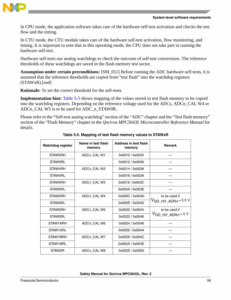
System-level software requirements
In CPU mode, the application software takes care of the hardware self-test activation and checks the test flow and the timing.
In CTU mode, the CTU module takes care of the hardware self-test activation, flow monitoring, and timing. It is important to note that in this operating mode, the CPU does not take part in running the hardware self-test.
Hardware self-tests use analog watchdogs to check the outcome of self-test conversions. The reference thresholds of these watchdogs are saved in the flash memory test sector.
Assumption under certain preconditions: [SM_051] Before running the ADC hardware self-tests, it is assumed that the reference thresholds are copied from “test flash” into the watchdog registers (STAWxR).[end]
Rationale: To set the correct threshold for the self-tests.
Implementation hint: Table 5-5 shows mapping of the values stored in test flash memory to be copied into the watchdog registers. Depending on the reference voltage used for the ADCs, ADCn_CAL W4 or ADCn_CAL W5 is to be used for ADC_n_STAW0R.
Please refer to the “Self-test analog watchdog” section of the “ADC” chapter and the “Test flash memory” section of the “Flash Memory” chapter in the Qorivva MPC5643L Microcontroller Reference Manual for details.
Table 5-5. Mapping of test flash memory values to STAWxR
Watchdog registerName in test flash
memoryAddress in test flash
memoryRemark
STAW3RH ADCn_CAL W1 0x0010 / 0x0034 —
STAW3RL 0x0012 / 0x0036 —
STAW4RH ADCn_CAL W2 0x0014 / 0x0038 —
STAW4RL 0x0016 / 0x003A —
STAW5RH ADCn_CAL W3 0x0018 / 0x003C —
STAW5RL 0x000A / 0x003E —
STAW0RH ADCn_CAL W4 0x000C / 0x0040 to be used ifVDD_HV_ADRn = 3.3 V
STAW0RL 0x000E / 0x0042
STAW0RH ADCn_CAL W5 0x0020 / 0x0044 to be used ifVDD_HV_ADRn = 5 V
STAW0RL 0x0022 / 0x0046
STAW1ARH ADCn_CAL W6 0x0024 / 0x0048 —
STAW1ARL 0x0026 / 0x004A —
STAW1BRH ADCn_CAL W7 0x0028 / 0x004C —
STAW1BRL 0x002A / 0x004E —
STAW2R ADCn_CAL W8 0x002E / 0x0050 —
Safety Manual for Qorivva MPC5643L, Rev. 2
Freescale Semiconductor 56

System-level software requirements
Implementation hint: Because test flash memory cannot be read directly, the Test Flash Enable feature of the SSCM may be exploited. This action is performed through the following steps:
1. If code is executed out of flash memory, CPU branches into RAM and executes code out of SRAM memory.
2. Write SSCM_SCTR[TFE] = 1.
3. Test sector is readable at the offset 0x0 of the flash memory address space (See “System Status and Configuration Module (SSCM)” of the Qorivva MPC5643L Microcontroller Reference Manual).
4. Thresholds are copied from the Test sector to the respective register.
5. Write SSCM_SCTR[TFE] = 0.
6. Code can continue execution out of flash memory.
NOTEAs the BAM is not developed following an ISO compliant software process, system integrators are asked to avoid reading the test sector through the BAM access method. Please refer to Section 5.2.19, System Status and Configuration Module (SSCM) for details.
Assumption under certain preconditions: [SM_052] When using integrated self-test as the functional safety integrity measure, it is assumed that the analog watchdog timer for CPU mode and CTU mode must be enabled for the self-test. The programmable watchdog timeout is smaller than the FTTI.[end]
Rationale: To check the correct completion of the ADC self-test algorithms.
Implementation hint: Every hardware BIST is activated via a dedicated command sent to the ADC (see the “Self-testing” section in the “ADC” chapter of the Qorivva MPC5643L Microcontroller Reference Manual for details on implementing these tests).
The SUPPLY SELF-TEST is executed without interleaved conversion.
Due to their analog parts, the ADCs require additional tests implemented in software. Please refer to Section 5.3.3, Analog inputs.
5.2.26.2 Runtime checks
Dependent on required fault coverage, it might be necessary to execute SUPPLY SELF-TEST, RESISTIVE-CAPACITIVE SELF-TEST, and CAPACITIVE SELF-TEST also once per FTTI (for example, when using a Single Read Analog Input (Section 5.3.3.1.1, Single-read analog inputs)).
5.3 I/O functionsThe integrity of functional safety relevant periphery is mainly ensured by application level measures (for example, connecting one sensor to different I/O modules, sensor validation by sensor fusion).
Functional safety relevant peripherals are assumed to be used redundantly in some way. Different approaches can be used, for example, by implementing replicated input (for example, connect one sensor to two DSPIs or even connect two sensors measuring the same quantity to two ADCs) or by crosschecking some I/O operations with different operations (for example, using sensor values of different quantities to
Safety Manual for Qorivva MPC5643L, Rev. 2
Freescale Semiconductor57

System-level software requirements
check for validity). Preferably, the replicated modules generate or receive the replicated data using different coding styles (for example, inverted in the voltage domain or using voltage and time domain coding for redundant channels). System integrators may choose the approach that best fits their needs.
Assumption under certain preconditions: [SM_038] If system level requires specific robustness regarding Common Mode Faults within the I/O peripheral system, respective measures are assumed on system level.[end]
Rationale: To improve the Common Mode Fault robustness of the I/O.
Implementation hint: Possible measures could use different coding schemes within each redundant I/O channel (for example, inverted signals, different time periods).
Implementation hint: Possible measures could be using different replicated peripherals (for example, eTimer_0, eTimer_1, or FlexPWM) to implement multiple independent and different channels.
Peripherals (for example, SIUL, FlexPWM, or the eTimer) used for the functional safety function must be configured properly before their usage. Any misconfiguration prevents them from delivering the expected functionality.
Assumption under certain preconditions: [SM_019] When safety functions use digital GPIO, it is assumed that the pads are configured by writing the appropriate values to the GPIOs corresponding SIUL_PCRn.[end]
Rationale: To configure GPIO used by the safety functions and to reduce the likelihood of CMF caused by improper configuration of the GPIO.
5.3.1 Digital inputs
5.3.1.1 Hardware
Functional safety digital inputs may to be acquired redundantly.
• Double read operation of a digital input is implemented by two general purpose inputs (GPI) of the SIUL unit. A comparison (by software) between the double reads detects an error (please refer to Figure 5-13).
• A double read PWM input is implemented by using two modules as two channels. The functional safety integrity is achieved by double reads and a software comparison. One channel is provided by eTimer_0 and the other by eTimer_1 or eTimer_2. The usage of eTimer_1 and eTimer_2 is also possible. Read PWM input means any input read related to signal transitions (rise or fall). This may also include the time that the signal was high, low or both (refer to Figure 5-13).
• A double read eTimer input is implemented by using two modules as two channels. The functional safety integrity is achieved by double reads and a software comparison. One channel is provided by eTimer_0 and the other by eTimer_1 or eTimer_2. The usage of eTimer_1 and eTimer_2 is also possible. Read Encoder Input means any input read elated to signal transitions (rise or fall). This may also include signals coming from an encoder (please refer to Figure 5-14).
For double read eTimer input, each signal, the SIUL can provide additional channels to support interrupt-based reading for each signal.
Safety Manual for Qorivva MPC5643L, Rev. 2
Freescale Semiconductor 58
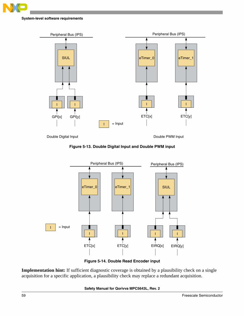
System-level software requirements
Figure 5-13. Double Digital Input and Double PWM input
Figure 5-14. Double Read Encoder input
Implementation hint: If sufficient diagnostic coverage is obtained by a plausibility check on a single acquisition for a specific application, a plausibility check may replace a redundant acquisition.
Double PWM Input
ETC[x] ETC[y]
eTimer_0 eTimer_1
I I
I = Input
Peripheral Bus (IPS)
SIUL
I
Double Digital Input
I
GPI[y]GPI[x]
Peripheral Bus (IPS)
eTimer_0
I
ETC[x]
eTimer_1
I
ETC[y]
SIUL
II
EIRQ[x] EIRQ[y]
Peripheral Bus (IPS)Peripheral Bus (IPS)
I = Input
Safety Manual for Qorivva MPC5643L, Rev. 2
Freescale Semiconductor59

System-level software requirements
5.3.1.2 Software
Digital inputs used for functional safety purposes are assumed to be input redundantly as described in this section. Table 5-6 lists three element safety functions for input, the corresponding safety integrity functions, and their execution frequency. Alternative solutions with sufficient diagnostic coverage are possible.
5.3.1.2.1 Double Read Digital Inputs
Rationale: To check that the configuration of the two I/Os used correspond with the expected configuration, to reduce the likelihood of CMF caused by incorrectly configured I/Os, and to check that the two input values read are similar.
Implementation hint: Functional safety integrity is achieved by replicated reading and software comparison by the processing function. The application may implement the tests SIUL_SWTEST_REGCRC and GPI_SWTEST_CMP.
Implementation details
The only hardware element that can be used for the safety function is the general purpose I/O (GPIO).
Implementation hint: Every I/O that is not dedicated to a single function may be configured as GPIO. I/Os that are dedicated to ADC are an exception to this rule, as they can only be configured as inputs.
Redundant GPIO should be selected in a way that their signals are not adjacent, which helps minimize the likelihood of CMFs.
See Section 5.2.7, Cyclic Redundancy Checker Unit (CRC) for <module>_SWTEST_REGCRC implementation details.
Table 5-6. Digital inputs software tests
Function Test Frequency
Double Read Digital Inputs SIUL_SWTEST_REGCRC Once after programming
GPI_SWTEST_CMP Once for every acquisition
Double Read PWM Inputs ETIMER0_SWTEST_REGCRC Once after programming
ETIMER1_SWTEST_REGCRC Once after programming
SIUL_SWTEST_REGCRC Once after programming
ETIMERI_SWTEST_CMP Once for every acquisition
Double Read Encoder Inputs ETIMER0_SWTEST_REGCRC Once after programming
ETIMER1_SWTEST_REGCRC Once after programming
SIUL_SWTEST_REGCRC Once after programming
ENCI_SWTEST_CMP Once for every acquisition
Safety Manual for Qorivva MPC5643L, Rev. 2
Freescale Semiconductor 60

System-level software requirements
GPI_SWTEST_CMP
This software test is used to execute the comparison between the double reads performed by the independent channels, and reads the outputs sequentially. This allows any GPIO to be used, but could result in a wrong result if the state of the input changes between reading the first and second inputs.
An alternative implementation would be to use the parallel data input registers (PGPDI) in the same way that the GPODW_SWAPP_WRITE uses the output equivalent of these registers. This would allow the inputs to be read at the same point in time but would restrict the GPIO that could be used.
Please refer to Section 8.1.4.2, GPI_SWTEST_CMP for an implementation example.
5.3.1.2.2 Double Read PWM Inputs
Rationale: To check that the configuration of the modules used by this safety function compare to the expected configuration and to validate that the two sets of read data correlate.
Implementation hint: The software tests that the application may implement are:
• ETIMER0_SWTEST_REGCRC
• ETIMER1_SWTEST_REGCRC
• SIUL_SWTEST_REGCRC
In addition, the double reads should be compared by the application with the implementation of the following test:
• ETIMERI_SWTEST_CMP.
Implementation details
The following hardware elements may be used for the safety function:
• eTimer_0 channels
• eTimer_1 channels
• eTimer_2 channels
The system integrator may select one channel from different eTimers each.
See Section 5.2.7, Cyclic Redundancy Checker Unit (CRC) for <module>_SWTEST_REGCRC implementation details.
ETIMERI_SWTEST_CMP
This test is used to execute the comparison between the double reads of PWM inputs performed by two channels of different eTimers (for example, eTimer_0 and eTimer_1). The comparison may take into account possible approximations because of different capturing of the asynchronous input signals.
Please refer to Section 8.1.4.1, ETIMERI_SWTEST_CMP for an implementation example.
5.3.1.2.3 Double Read Encoder Inputs
Rationale: To reduce the risk of cascading faults due to shared resources.
Safety Manual for Qorivva MPC5643L, Rev. 2
Freescale Semiconductor61
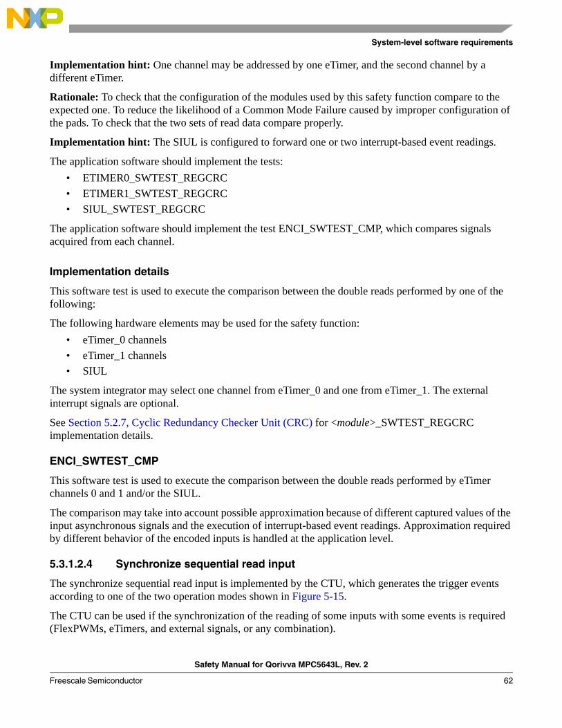
System-level software requirements
Implementation hint: One channel may be addressed by one eTimer, and the second channel by a different eTimer.
Rationale: To check that the configuration of the modules used by this safety function compare to the expected one. To reduce the likelihood of a Common Mode Failure caused by improper configuration of the pads. To check that the two sets of read data compare properly.
Implementation hint: The SIUL is configured to forward one or two interrupt-based event readings.
The application software should implement the tests:
• ETIMER0_SWTEST_REGCRC
• ETIMER1_SWTEST_REGCRC
• SIUL_SWTEST_REGCRC
The application software should implement the test ENCI_SWTEST_CMP, which compares signals acquired from each channel.
Implementation details
This software test is used to execute the comparison between the double reads performed by one of the following:
The following hardware elements may be used for the safety function:
• eTimer_0 channels
• eTimer_1 channels
• SIUL
The system integrator may select one channel from eTimer_0 and one from eTimer_1. The external interrupt signals are optional.
See Section 5.2.7, Cyclic Redundancy Checker Unit (CRC) for <module>_SWTEST_REGCRC implementation details.
ENCI_SWTEST_CMP
This software test is used to execute the comparison between the double reads performed by eTimer channels 0 and 1 and/or the SIUL.
The comparison may take into account possible approximation because of different captured values of the input asynchronous signals and the execution of interrupt-based event readings. Approximation required by different behavior of the encoded inputs is handled at the application level.
5.3.1.2.4 Synchronize sequential read input
The synchronize sequential read input is implemented by the CTU, which generates the trigger events according to one of the two operation modes shown in Figure 5-15.
The CTU can be used if the synchronization of the reading of some inputs with some events is required (FlexPWMs, eTimers, and external signals, or any combination).
Safety Manual for Qorivva MPC5643L, Rev. 2
Freescale Semiconductor 62
System-level software requirements
Assumption under certain preconditions: [SM_047] If the CTU is part of an application safety function, it is assumed that system level functional safety integrity measures have to be implemented to achieve required integrity. [end]
Rationale: To validate the integrity of the CTU.
Implementation hint: The following mix of hardware mechanisms and software safety integrity functions implemented at the application level provide respective functional safety integrity:
• CTU_HWSWTEST_TRIGGERNUM
• CTU_SWTEST_TRIGGERTIME
• CTU_HWSWTEST_TRIGGEROVERRUN
• CTU_HWSWTEST_ADCCOMMAND (only if the input is an analog signal)
• CTU_SWTEST_ETIMERCOMMAND
• CTU_HW_CFGINTEGRITY
Hardware element
Figure 5-15. CTU operating modes: triggered (a) and sequential (b)
The CTU receives various incoming signals (Event X in Figure 5-15) from different sources (FlexPWMs, eTimers, or external GPIO, or any combination). These signals are then processed to generate trigger events (Trigger X in Figure 5-15). An event can be a rising edge, a falling edge or both edges of each incoming signal. The output trigger can be a pulse, an ADC command (or a stream of consecutive commands), or both to one or more peripherals (for example, ADC, eTimers, and so on).
Delay T0
Delay T1
Delay T2
Delay T3
Delay T0
Delay T2
Delay T3
Delay T1
Event 0 Trigger 0 . . . . . . Event 3 Trigger 3
b)
Event Trigger0 Trigger 1 Trigger 2 Trigger 3 Event
a)
Safety Manual for Qorivva MPC5643L, Rev. 2
Freescale Semiconductor63

System-level software requirements
In triggered mode, the input event, which can also be a combination (logical OR) of several signals, determines the reload/restart of the CTU counter and up to eight comparators are available to generate up to eight output triggers with a given delay with respect to the reload signal. In sequential mode, one comparator can be used to generate a trigger with a given delay with respect to one out of eight input events (Event 0 works as the reload event).
Implementation hint: The CTU is configured so that the output triggers are generated with the desired time schedule with respect to the input event(s).
For each trigger, the set of ADC commands and pulses to be generated are defined.
Particularly, each ADC command specifies: which channel is acquired by which ADC, if two ADCs perform a concurrent conversion or if just one of them is operational, and in which CTU internal FIFO the result(s) will be stored. Four FIFOs are available (2 × 16 + 2 × 4). In the case of a concurrent acquisition, the same FIFO is used for both results. ADCs are configured to accept commands from the CTU (instead of commands provided via software). Multiple single or concurrent acquisitions can be scheduled for each trigger events (overall 24 commands per control period, for example, between two successive reload signals). The next command is sent when the ADC signals the completion of the previous acquisition.
Recommendation: The CTU can be configured to generate interrupt requests when a trigger occurs (for example, to trigger READ DIGITAL INPUTS).
Implementation details
The following hardware elements may be used for the safety function:
• CTU
• One eTimer channel
5.3.2 Digital outputs
Functional safety digital outputs are always assumed to be written either redundantly or with readback. In the case of a single output with readback, the feedback loop should be as large as possible to also cover faults at the system level. Figure 5-16 depicts the connection of two (functional safety critical) actuators connected to the MPC5643L. Actuator 1 is connected to an output peripheral (for example, a motor is connected to a PWM-output (output peripheral 3)). The signal generated by output peripheral 3 can be input to an input peripheral (for example, an eTimer). This measure is to confirm that the generated output
Table 5-7. CTU software tests
Function Test Frequency
Synchronize sequential read input
CTU_HWSWTEST_TRIGGERNUM Once for every control period (< FTTI)
CTU_SWTEST_TRIGGERTIME Once for every CTU control period (triggered mode) or every trigger (sequential mode)
CTU_HWSWTEST_TRIGGEROVERRUN Once for every trigger
CTU_HWSWTEST_ADCCOMMAND Once for every ADC command
CTU_SWTEST_ETIMERCOMMAND Once for every control period (< FTTI)
CTU_HW_CFGINTEGRITY Once for every control period (< FTTI)
Safety Manual for Qorivva MPC5643L, Rev. 2
Freescale Semiconductor 64
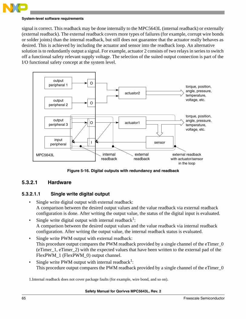
System-level software requirements
signal is correct. This readback may be done internally to the MPC5643L (internal readback) or externally (external readback). The external readback covers more types of failures (for example, corrupt wire bonds or solder joints) than the internal readback, but still does not guarantee that the actuator really behaves as desired. This is achieved by including the actuator and sensor into the readback loop. An alternative solution is to redundantly output a signal. For example, actuator 2 consists of two relays in series to switch off a functional safety relevant supply voltage. The selection of the suited output connection is part of the I/O functional safety concept at the system level.
Figure 5-16. Digital outputs with redundancy and readback
5.3.2.1 Hardware
5.3.2.1.1 Single write digital output
• Single write digital output with external readback:A comparison between the desired output values and the value readback via external readback configuration is done. After writing the output value, the status of the digital input is evaluated.
• Single write digital output with internal readback1:A comparison between the desired output values and the value readback via internal readback configuration. After writing the output value, the internal readback status is evaluated.
• Single write PWM output with external readback:This procedure output compares the PWM readback provided by a single channel of the eTimer_0 (eTimer_1, eTimer_2) with the expected values that have been written to the external pad of the FlexPWM_1 (FlexPWM_0) output channel.
• Single write PWM output with internal readback1:This procedure output compares the PWM readback provided by a single channel of the eTimer_0
1.Internal readback does not cover package faults (for example, wire bond, and so on).
O
inputperipheral
outputperipheral 2
outputperipheral 1
outputperipheral 3
O
O
I
actuator2
actuator1
sensor
torque, position,angle, pressure,temperature,voltage, etc.
torque, position,angle, pressure,temperature,voltage, etc.
internalreadback
externalreadback
external readbackwith actuator/sensor
in the loop
MPC5643L
Safety Manual for Qorivva MPC5643L, Rev. 2
Freescale Semiconductor65
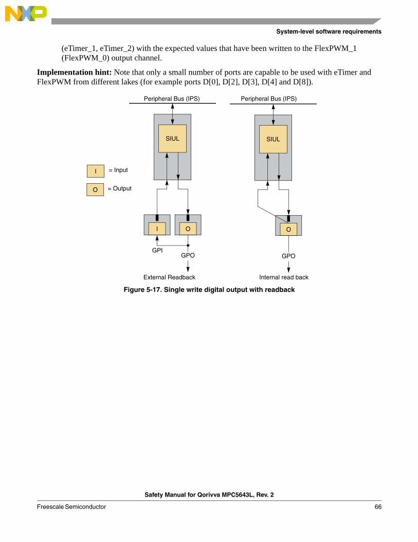
System-level software requirements
(eTimer_1, eTimer_2) with the expected values that have been written to the FlexPWM_1 (FlexPWM_0) output channel.
Implementation hint: Note that only a small number of ports are capable to be used with eTimer and FlexPWM from different lakes (for example ports D[0], D[2], D[3], D[4] and D[8]).
Figure 5-17. Single write digital output with readback
SIUL
OI
GPO
SIUL
O
GPO
I = Input
O = Output
GPI
External Readback Internal read back
Peripheral Bus (IPS) Peripheral Bus (IPS)
Safety Manual for Qorivva MPC5643L, Rev. 2
Freescale Semiconductor 66

System-level software requirements
Figure 5-18. Single write PWM output with readback
5.3.2.1.2 Double write digital output
• Double Write Digital OutputThe SIUL hardware element is used to perform a double write digital output (see Figure 5-19).
• Double Write PWM OutputThe following hardware elements may be used to perform a double write PWM output (see Figure 5-20):
— eTimer_0 and eTimer_1
— eTimer_0 and eTimer_2
— eTimer_1 and eTimer_2
— FlexPWM_0 and FlexPWM_1
eTimer
I
Peripheral Bus (IPS)
FlexPWM
eTimer
I
Peripheral Bus (IPS)
FlexPWM
OO
ETC[x]n[z] n[z]
I = Input
O = Output
external read back internal read back
Safety Manual for Qorivva MPC5643L, Rev. 2
Freescale Semiconductor67
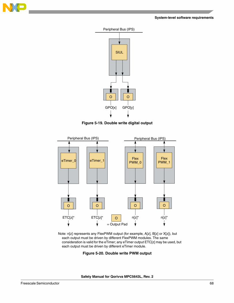
System-level software requirements
Figure 5-19. Double write digital output
Figure 5-20. Double write PWM output
SIUL
O
Peripheral Bus (IPS)
O
GPO[y]GPO[x]
eTimer_0
Peripheral Bus (IPS)
O
eTimer_1
O
Flex
O
Flex
O
PWM_0 PWM_1
ETC[z]* O
= Output Pad
ETC[z]* n[z]* n[z]*
Note: n[z] represents any FlexPWM output (for example, A[z], B[z] or X[z]), but each output must be driven by different FlexPWM modules. The same consideration is valid for the eTimer; any eTimer output ETC[z] may be used, but each output must be driven by different eTimer module.
Peripheral Bus (IPS)
Safety Manual for Qorivva MPC5643L, Rev. 2
Freescale Semiconductor 68

System-level software requirements
5.3.2.2 Software
Digital outputs used for functional safety purposes are assumed to be written either redundantly or with readback as described in this section. Table 5-8 lists four element safety functions for output, the corresponding safety integrity functions, and their execution frequency. Alternative solutions with sufficient diagnostic coverage are possible.
5.3.2.2.1 Single write digital outputs with readback
The SIUL hardware element is used to perform a single write digital output with readback (see Figure 5-17).
Rationale: To check whether written data is coherent to the expected data.
Implementation hint: The readback may be implemented either with external or with internal readback.
Table 5-8. Digital outputs software tests
Function Test Frequency
Single write digital outputs with readback
SIUL_SWTEST_REGCRC Once after programming
GPOERB_SWTEST_CMP Once every write
GPOIRB_SWTEST_CMP Once every write
Double write digital outputs SIUL_SWTEST_REGCRC Once after programming
GPODW_SWAPP_WRITE Once every write
Single write PWM outputs with readback
SIUL_SWTEST_REGCRC Once after programming
ETIMER0_SWTEST_REGCRC1
1 This test is needed only if the eTimer channels are used for the safety function.
Once after programming
ETIMER1_SWTEST_REGCRC1 Once after programming
ETIMER2_SWTEST_REGCRC1 Once after programming
FLEXPWM0_SWTEST_REGCRC2
2 This test is needed only if the FlexPWM channels are used for the safety function.
Once after programming
FLEXPWM1_SWTEST_REGCRC2 Once after programming
PWMRB_SWTEST_CMP Once every write
Double write PWM outputs SIUL_SWTEST_REGCRC Once after programming3
3 If a change in a single SIUL configuration register is capable of affecting both the output and the read-back paths, then SIUL_SWTEST_REGCRC is to be executed every PST. In all other cases, configuration errors are covered by the software comparison.
ETIMER0_SWTEST_REGCRC1 Once after programming
ETIMER1_SWTEST_REGCRC1 Once after programming
ETIMER2_SWTEST_REGCRC1 Once after programming
FLEXPWM0_SWTEST_REGCRC2 Once after programming
FLEXPWM1_SWTEST_REGCRC2 Once after programming
PWMDW_SWAPP_WRITE Once every write
Safety Manual for Qorivva MPC5643L, Rev. 2
Freescale Semiconductor69
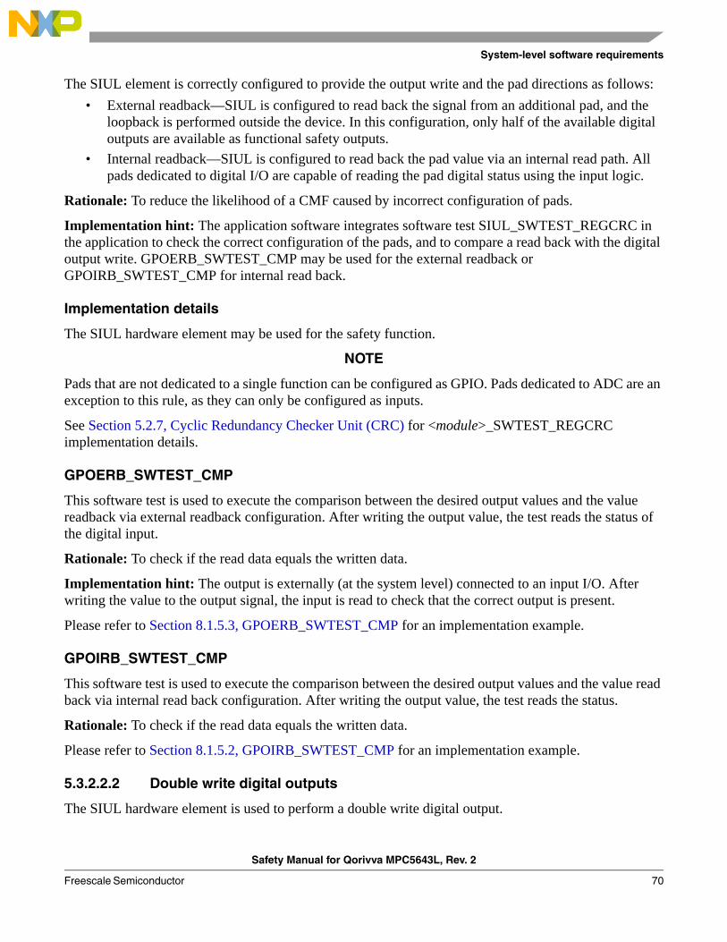
System-level software requirements
The SIUL element is correctly configured to provide the output write and the pad directions as follows:
• External readback—SIUL is configured to read back the signal from an additional pad, and the loopback is performed outside the device. In this configuration, only half of the available digital outputs are available as functional safety outputs.
• Internal readback—SIUL is configured to read back the pad value via an internal read path. All pads dedicated to digital I/O are capable of reading the pad digital status using the input logic.
Rationale: To reduce the likelihood of a CMF caused by incorrect configuration of pads.
Implementation hint: The application software integrates software test SIUL_SWTEST_REGCRC in the application to check the correct configuration of the pads, and to compare a read back with the digital output write. GPOERB_SWTEST_CMP may be used for the external readback or GPOIRB_SWTEST_CMP for internal read back.
Implementation details
The SIUL hardware element may be used for the safety function.
NOTE
Pads that are not dedicated to a single function can be configured as GPIO. Pads dedicated to ADC are an exception to this rule, as they can only be configured as inputs.
See Section 5.2.7, Cyclic Redundancy Checker Unit (CRC) for <module>_SWTEST_REGCRC implementation details.
GPOERB_SWTEST_CMP
This software test is used to execute the comparison between the desired output values and the value readback via external readback configuration. After writing the output value, the test reads the status of the digital input.
Rationale: To check if the read data equals the written data.
Implementation hint: The output is externally (at the system level) connected to an input I/O. After writing the value to the output signal, the input is read to check that the correct output is present.
Please refer to Section 8.1.5.3, GPOERB_SWTEST_CMP for an implementation example.
GPOIRB_SWTEST_CMP
This software test is used to execute the comparison between the desired output values and the value read back via internal read back configuration. After writing the output value, the test reads the status.
Rationale: To check if the read data equals the written data.
Please refer to Section 8.1.5.2, GPOIRB_SWTEST_CMP for an implementation example.
5.3.2.2.2 Double write digital outputs
The SIUL hardware element is used to perform a double write digital output.
Safety Manual for Qorivva MPC5643L, Rev. 2
Freescale Semiconductor 70

System-level software requirements
Rationale: To configure GPIO used by this safety function and reduce the likelihood of a CMF caused by incorrect configuration of the GPIO.
Implementation hint: The SIUL is configured by application software to correctly define the configuration of the outputs used. The software performs a double write.
Rationale: To reduce the likelihood of a CMF caused by incorrect configuration of the GPIO.
Implementation hint: To achieve the integrity of the two output channels, the application validates the SIUL configuration implementing the SIUL_SWTEST_REGCRC.
Rationale: To write a digital output by exploiting redundancy.
Implementation hint: The application software implements the double output write as defined by the GPODW_SWAPP_WRITE.
Implementation details
The only hardware element that can be used for the safety function is the GPIO.
Every I/O that is not dedicated to a single function may be configured as GPIO. I/Os that are dedicated to ADC are an exception to this rule, as they can only be configured as inputs.
See Section 5.2.7, Cyclic Redundancy Checker Unit (CRC) for <module>_SWTEST_REGCRC implementation details.
GPODW_SWAPP_WRITE
Implementation hint: The output write of a redundant channel may be implemented by writing the two outputs with a single instruction to the appropriate register and this register may be checked by readback.
To write two or more GPIOs with a single instruction, the Masked Parallel GPIO Pad Data Out register (SIUL_MPGPDOn) register can be used. The two GPIOs used must be in the same SIUL_MPGPDOn register.
To protect the value of the other GPIOs that belong to the same SIUL_MPGPDOn, the MASK field of the SIUL_MPGPDOn register needs to be properly configured.
When using a single write (atomic) instruction to SIUL_MPGPDOn register, it is good practice to read back (read after write) the register content due to the fact that a transient fault in the SIUL IPS interface can affect in principle both output channels. The readback is needed to cover this common mode of failure. An alternative implementation would be to write the two outputs separately not using the parallel register, resulting in a small delay in output change between the channels.
Please refer to Section 8.1.5.1, GPODW_SWAPP_WRITE for an implementation example.
5.3.2.2.3 Single write PWM outputs with readback
The following combination of elements may be used to perform a write PWM output with readback:
• eTimer_0 – FlexPWM_1
• eTimer_1 – FlexPWM_0
Safety Manual for Qorivva MPC5643L, Rev. 2
Freescale Semiconductor71
System-level software requirements
• eTimer_2 – FlexPWM_0
• eTimer_2 – FlexPWM_1
These units are configured to implement one PWM output channel and (via internal readback) the eTimer_0 input PWM channel. The SIUL is configured to define the configuration of the output pads used. The software performs a write operation followed by a read operation. To achieve the integrity of the input and output channels, the application tests the SIUL configuration implementing the SIUL_SWTEST_REGCRC (to reduce the likelihood of a Common Mode Failure caused by incorrect configuration of the pads).
Rationale: To check that the configuration of the modules used by this safety function adheres to the expected configuration.
Implementation hint: A single channel of the eTimer is used with a multiplexing of the internal readback of the different output of the FlexPWM. The readback paths are limited to six signals, two for each submodule of the FlexPWM.
The following tests validate correct configurations:
• FLEXPWM0_SWTEST_REGCRC
• FLEXPWM1_SWTEST_REGCRC
• ETIMER0_SWTEST_REGCRC
• ETIMER1_SWTEST_REGCRC
• ETIMER2_SWTEST_REGCRC
• SIUL_SWTEST_REGCRC
Rationale: To check that the written data is what is expected.
Implementation hint: The application software writes to the output port and then compare the written value via the readback (PWMRB_SWTEST_CMP).
Implementation details
The following hardware elements may be used for the safety function:
• eTimer_0 channels
• eTimer_1 channels
• eTimer_2 channels
• FlexPWM_0 channels
• FlexPWM_1 channels
eTimer_0 should not be used in combination with FlexPWM_0 (eTimer_1 and FlexPWM_1) due to the same lake assignment (please refer to Section 7.1, Causes of dependent failures).
See Section 5.2.7, Cyclic Redundancy Checker Unit (CRC) for <module>_SWTEST_REGCRC implementation details.
Safety Manual for Qorivva MPC5643L, Rev. 2
Freescale Semiconductor 72
System-level software requirements
PWMRB_SWTEST_CMP
This test compares the PWM readback provided by a single channel of the eTimer_1 (eTimer_0) with the expected values that have been written to the FlexPWM_0 (FlexPWM_1) output channel.
For this example, FlexPWM_0 is used to generate a PWM output and eTimer_1 is used to read back and verify the output. Another combination could be used if required in an application.
Please refer to Section 8.1.5.4, PWMRB_SWTEST_CMP for an implementation example.
5.3.2.2.4 Double write PWM outputs
The hardware elements eTimer_0 and eTimer_1 or FlexPWM_0 and FlexPWM_1 are used to perform a double Write PWM Output.
Configuring these units to implement two independent PWM channels. The SIUL must be configured to define the configuration of the output pads used. The software must perform a double write.
Rationale: To write a PWM output by exploiting redundancy.
Implementation hint: Configuring these units to implement two independent PWM channels. The SIUL is configured to define the configuration of the output pads used. The software performs a double write (PWMDW_SWAPP_WRITE).
Rationale: To reduce the likelihood of a CMF caused by incorrect configuration of the pads.
Implementation hint: To improve the integrity of the two output channels, the application should test the SIUL configuration implementing the SIUL_SWTEST_REGCRC.
Rationale: To check that the configuration of the modules used by this safety function adheres to the expected configuration.
Implementation hint: The application software may implement a test for the register configuration:
• ETIMER0_SWTEST_REGCRC (for eTimer)
• ETIMER1_SWTEST_REGCRC (for eTimer)
• ETIMER2_SWTEST_REGCRC (for eTimer)
• FLEXPWM0_SWTEST_REGCRC (for FlexPWM)
• FLEXPWM1_SWTEST_REGCRC (for FlexPWM)
• SIUL_SWTEST_REGCRC
Rationale: To reduce the possibility of a Cascading Failure to shared circuitries, different modules should be used.
Implementation hint: The output write of a redundant PWM channel is implemented by writing the new output values to both PWM channels. The system integrator can decide whether to use two of the three eTimers (eTimer_0, eTimer_1, eTimer_2) or both FlexPWMs (FlexPWM_0, FlexPWM_1).
Safety Manual for Qorivva MPC5643L, Rev. 2
Freescale Semiconductor73
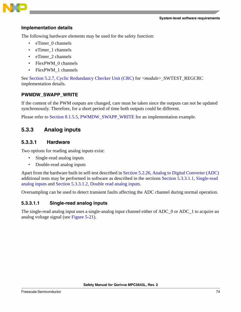
System-level software requirements
Implementation details
The following hardware elements may be used for the safety function:
• eTimer_0 channels
• eTimer_1 channels
• eTimer_2 channels
• FlexPWM_0 channels
• FlexPWM_1 channels
See Section 5.2.7, Cyclic Redundancy Checker Unit (CRC) for <module>_SWTEST_REGCRC implementation details.
PWMDW_SWAPP_WRITE
If the content of the PWM outputs are changed, care must be taken since the outputs can not be updated synchronously. Therefore, for a short period of time both outputs could be different.
Please refer to Section 8.1.5.5, PWMDW_SWAPP_WRITE for an implementation example.
5.3.3 Analog inputs
5.3.3.1 Hardware
Two options for reading analog inputs exist:
• Single-read analog inputs
• Double-read analog inputs
Apart from the hardware built-in self-test described in Section 5.2.26, Analog to Digital Converter (ADC) additional tests may be performed in software as described in the sections Section 5.3.3.1.1, Single-read analog inputs and Section 5.3.3.1.2, Double read analog inputs.
Oversampling can be used to detect transient faults affecting the ADC channel during normal operation.
5.3.3.1.1 Single-read analog inputs
The single-read analog input uses a single-analog input channel either of ADC_0 or ADC_1 to acquire an analog voltage signal (see Figure 5-21).
Safety Manual for Qorivva MPC5643L, Rev. 2
Freescale Semiconductor 74
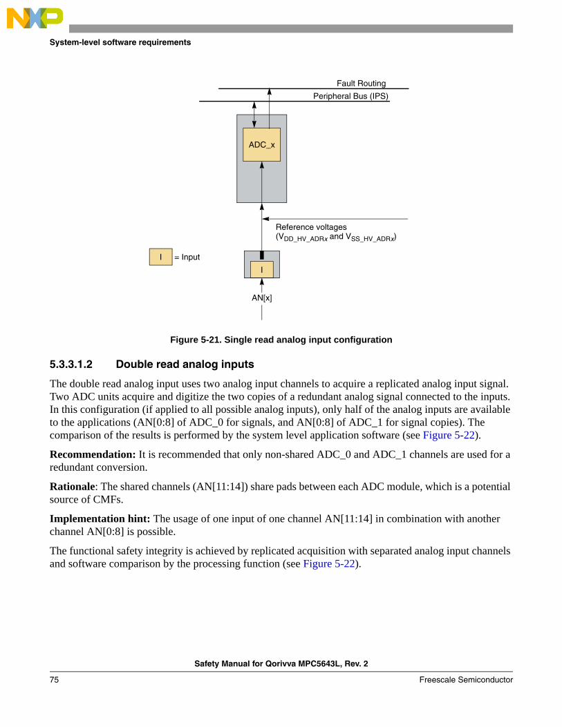
System-level software requirements
Figure 5-21. Single read analog input configuration
5.3.3.1.2 Double read analog inputs
The double read analog input uses two analog input channels to acquire a replicated analog input signal. Two ADC units acquire and digitize the two copies of a redundant analog signal connected to the inputs. In this configuration (if applied to all possible analog inputs), only half of the analog inputs are available to the applications (AN[0:8] of ADC_0 for signals, and AN[0:8] of ADC_1 for signal copies). The comparison of the results is performed by the system level application software (see Figure 5-22).
Recommendation: It is recommended that only non-shared ADC_0 and ADC_1 channels are used for a redundant conversion.
Rationale: The shared channels (AN[11:14]) share pads between each ADC module, which is a potential source of CMFs.
Implementation hint: The usage of one input of one channel AN[11:14] in combination with another channel AN[0:8] is possible.
The functional safety integrity is achieved by replicated acquisition with separated analog input channels and software comparison by the processing function (see Figure 5-22).
ADC_x
Fault Routing
Peripheral Bus (IPS)
AN[x]
Reference voltages(VDD_HV_ADRx and VSS_HV_ADRx)
I
I = Input
Safety Manual for Qorivva MPC5643L, Rev. 2
Freescale Semiconductor75
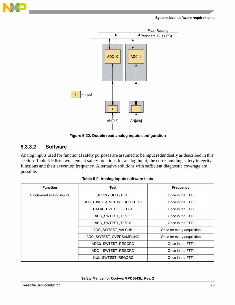
System-level software requirements
Figure 5-22. Double read analog inputs configuration
5.3.3.2 Software
Analog inputs used for functional safety purposes are assumed to be input redundantly as described in this section. Table 5-9 lists two element safety functions for analog input, the corresponding safety integrity functions and their execution frequency. Alternative solutions with sufficient diagnostic coverage are possible.
Table 5-9. Analog inputs software tests
Function Test Frequency
Single-read analog inputs SUPPLY SELF-TEST Once in the FTTI
RESISTIVE-CAPACITIVE SELF-TEST Once in the FTTI
CAPACITIVE SELF-TEST Once in the FTTI
ADC_SWTEST_TEST1 Once in the FTTI
ADC_SWTEST_TEST2 Once in the FTTI
ADC_SWTEST_VALCHK Once for every acquisition
ADC_SWTEST_OVERSAMPLING Once for every acquisition
ADC0_SWTEST_REGCRC Once in the FTTI
ADC1_SWTEST_REGCRC Once in the FTTI
SIUL_SWTEST_REGCRC Once in the FTTI
ADC_0
AN[0:8]
ADC_1
AN[0:8]
I I
Fault Routing
Peripheral Bus (IPS)
I = Input
Safety Manual for Qorivva MPC5643L, Rev. 2
Freescale Semiconductor 76

System-level software requirements
5.3.3.2.1 Single-read analog inputs
To support a high diagnostic coverage, two known reference supply voltages are used by two software tests which are described in the following sections (ADC_SWTEST_TEST1 and ADC_SWTEST_TEST2).
The reference supply voltages are the following:
• VDD_HV_ADR0 (ADC_0 high reference voltage)
• VDD_HV_ADR1 (ADC_1 high reference voltage)
• VSS_HV_ADR0 (ADC_0 low reference voltage)
• VSS_HV_ADR1 (ADC_1 low reference voltage)
The SIUL unit is configured to correctly enable the ADC inputs. The pads used for analog inputs can only be configured as inputs.
Single-read analog inputs may be implemented using the following safety integrity functions at the application level:
• ADC_SWTEST_TEST1
• ADC_SWTEST_TEST2
• ADC_SWTEST_VALCHK
• ADC0_SWTEST_REGCRC
• ADC1_SWTEST_REGCRC
• SIUL_SWTEST_REGCRC
• ADC_SWTEST_OVERSAMPLING
Assumption under certain preconditions: [SM_050] If ADC without redundant conversion is used, it is assumed that the functional safety integrity of the multiplexing circuit and bandgap is checked once per FTTI during runtime.[end]
Recommendation: It is recommended to execute ADC_SWTEST_TEST1 and ADC_SWTEST_TEST2 using presampling to detect open and short failures of the multiplexing circuit and failures in the bandgap.
Rationale: To check the integrity of the multiplexing circuit and bandgap.
Double-read analog inputs SUPPLY SELF-TEST Once after boot
RESISTIVE-CAPACITIVE SELF-TEST Once after boot
CAPACITIVE SELF-TEST Once after boot
ADC0_SWTEST_REGCRC Once after programming
ADC1_SWTEST_REGCRC Once after programming
SIUL_SWTEST_REGCRC Once after programming
ADC_SWTEST_CMP Once for every acquisition
Table 5-9. Analog inputs software tests (continued)
Function Test Frequency
Safety Manual for Qorivva MPC5643L, Rev. 2
Freescale Semiconductor77

System-level software requirements
Assumption under certain preconditions: [SM_708] If an ADC is used, it is assumed that the control and queue logic of the ADC and the CTU (if used) are checked for correct operation.[end]
Recommendation: It is recommended to implement the following test: ADC_SWTEST_VALCHK.
Recommendation: It is recommended acquire ADC data redundant in time (oversampling).
Rationale: As a countermeasure against random fault.
Implementation details
The following hardware elements may be used for the safety integrity functions:
• Analog input channels AN[0:8] of ADC_0
• Analog input channels AN[11:14] of ADC_0 and ADC_1 (shared channels)
• Analog input channels AN[0:8] of ADC_1
The system integrator may select one channel from ADC_0 or from ADC_1. Shared channels can be used.
See Section 5.2.7, Cyclic Redundancy Checker Unit (CRC) for <module>_SWTEST_REGCRC implementation details.
If ADC_0 is used, the ADC0_SWTEST_REGCRC may be used. If ADC_1 is used, the ADC1_SWTEST_REGCRC may be used.
ADC_SWTEST_TEST1 (open detection)
Reading the reference voltages before reading the channel to be acquired (presampling) detects open failures of the channel multiplexing circuitry. Misconfiguration of multiplexing circuitry (SIUL) may be detected. In addition, by comparison with the expected reference value, this test detects errors in the reference bandgap and possible errors of the ADCs control logic.
This test exploits the presampling feature of the ADC. Presampling allows the precharging or discharging of the ADC internal capacitor before it starts the sampling and conversion phases of the analog input received from the pads. During the presampling phase, the ADC samples the internally generated voltage. While in the sampling phase, the ADC samples analog input coming from the pads. In the conversion phase, the last sampled value is converted to a digital value. Figure 5-23 shows the normal sequence of operation for two channels (Presampling – Sampling – Conversion).
Figure 5-23. Implementation of ADC_SWTEST_TEST1
ConvertCh A
PresampleCh B
SampleCh B
ConvertCh B
PresampleCh A
SampleCh A t
VDD_HV_ADRn
VSS_HV_ADRn
Note: Either VDD_HV_ADR or VSS_HV_ADR can be used as presampling voltage.
or
Safety Manual for Qorivva MPC5643L, Rev. 2
Freescale Semiconductor 78

System-level software requirements
Reference voltages, which can be used during presampling phase, is either VDD_HV_ADR or VSS_HV_ADR.
If there is an open failure in the analog multiplexing circuitry, the signal converted by the ADC is not the analog input coming from the pad, but the presampling reference voltage (VDD_HV_ADRn or VSS_HV_ADRn). Figure 5-24 depicts the signal path in the analog multiplexing circuitry for presampling phase and conversion phase.
Figure 5-24. ADC_SWTEST_TEST1 (open detection)
Each analog input channel used by the safety function may be tested by system level measures (software).
Because the pads dedicated to analog inputs are of type INPUT, a missing enable from the SIUL results in an open failure.
Rationale: To detect open failures of the channel multiplexing circuitry (see Figure 5-24).
Implementation hint: Presampling can be enabled on a per channel basis through the ADC_n_PSR0 register. ADC_n_PCSR[PREVAL0] selects which reference voltage is used to precharge/discharge the ADC internal capacitor, (ADC_n_PSCR[PRECONV] = 0). (See the “Analog-to-Digital Converter (ADC)” chapter in the Qorivva MPC5643L Microcontroller Reference Manual for details on the presampling feature).
CAUTIONTo reduce the likelihood of a false indication of an open fault in the analog multiplexor, signals connected to the ADC inputs should not reach the reference voltages (VDD_HV_ADR, VSS_HV_ADR). In case this limitation cannot be fulfilled by the application, a more complex algorithm may be necessary (for example, run the test three times with VDD_HV_ADR, VSS_HV_ADR, VDD_HV_ADR).
Please refer to Section 8.1.6.1, ADC_SWTEST_TEST1 for an implementation example.
ADC_SWTEST_TEST2 (short detection)
To detect short failures, two different voltages are acquired by the ADC. If these values are different from the expected ones, a short failure on the multiplexed circuitry has been detected.
To implement this test, a presampling feature of the ADC can be exploited. The presampling may be configured in such a way that the sampling of the channel is bypassed and the presampling reference supply voltages are converted.
During the first step, the VDD_HV_ADRn is converted and compared with the expected value; then the VSS_HV_ADRn is converted and compared with the expected one (see Figure 5-25).
ADC
Referencevalue 1
pinsADC
Referencevalue 1
pinsADCADC
Presampling phase Conversion phase
Safety Manual for Qorivva MPC5643L, Rev. 2
Freescale Semiconductor79

System-level software requirements
Figure 5-25. Implementation of ADC_SWTEST_TEST2
Rationale: To detect short failures of the channel multiplexing circuitry (see Figure 5-26).
Figure 5-26. ADC_SWTEST_TEST2 (short detection)
Implementation hint: Presampling can be enabled on a per-channel basis through the ADC_n_PSR0 register. ADC_n_PCSR[PREVAL0] selects which reference voltage is used to precharge/discharge the ADC internal capacitor. To bypass the conversion of the input channel and convert the presampled values, ADC_n_PCSR[PRECONV] = 1. (See the “Analog-to-Digital Converter (ADC)” chapter in the Qorivva MPC5643L Microcontroller Reference Manual for details on the presampling feature).
Please refer to Section 8.1.6.2, ADC_SWTEST_TEST2 for an implementation example.
ADC_SWTEST_VALCHK
The goal of this software test is to verify correct operation of the control and queue logic of the ADC, and also the CTU, if used. The way this software measure is implemented depends on how the ADC is configured (for example, CTU or CPU mode):
• When the ADC is used in CPU mode, the acquired value is read by the ADC_CDRn. This register includes ADC_CDRn[VALID] and ADC_CDRn[RESULT] fields as well as channel n converted data (ADC_CDRn[CDATA]). These fields provide status information about the data acquisition. Application software should read and verify these fields after every acquisition.
• When ADC conversion is triggered by the CTU, the acquired digital sample data is stored into a dual queue along with information about the channel that performed the acquisition. The checking of the expected channel provides coverage of the control logic and part of the queue logic.
Implementation hint: If ADC is configured to work in CTU mode, the conversion results are stored in CTU FIFOs (see the CTU chapter in Qorivva MPC5643L Microcontroller Reference Manual for details). Along with the converted data, the converted channel number and ADC module are stored. CTU includes two sets of registers to read this information (FIFO right-aligned data, FRx, and FIFO right-aligned data, FLx). These registers may be read to check that the sequence of the acquired channel is what is expected.
PresampleCh x
ConvertCh x
PresampleCh x
ConvertCh x t
VDD_HV_ADRx VSS_HV_ADRx
Note: Either VDD_HV_ADR or VSS_HV_ADR can be used as presampling voltage.
ADC
Referencevalue 2
pinsADC
Referencevalue 1
pins ADCADC
ADC
Referencevalue 1
First reference conversion Second reference conversion
pins
Safety Manual for Qorivva MPC5643L, Rev. 2
Freescale Semiconductor 80
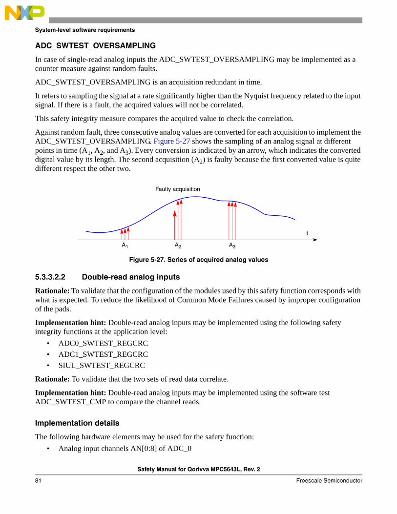
System-level software requirements
ADC_SWTEST_OVERSAMPLING
In case of single-read analog inputs the ADC_SWTEST_OVERSAMPLING may be implemented as a counter measure against random faults.
ADC_SWTEST_OVERSAMPLING is an acquisition redundant in time.
It refers to sampling the signal at a rate significantly higher than the Nyquist frequency related to the input signal. If there is a fault, the acquired values will not be correlated.
This safety integrity measure compares the acquired value to check the correlation.
Against random fault, three consecutive analog values are converted for each acquisition to implement the ADC_SWTEST_OVERSAMPLING. Figure 5-27 shows the sampling of an analog signal at different points in time (A1, A2, and A3). Every conversion is indicated by an arrow, which indicates the converted digital value by its length. The second acquisition (A2) is faulty because the first converted value is quite different respect the other two.
Figure 5-27. Series of acquired analog values
5.3.3.2.2 Double-read analog inputs
Rationale: To validate that the configuration of the modules used by this safety function corresponds with what is expected. To reduce the likelihood of Common Mode Failures caused by improper configuration of the pads.
Implementation hint: Double-read analog inputs may be implemented using the following safety integrity functions at the application level:
• ADC0_SWTEST_REGCRC
• ADC1_SWTEST_REGCRC
• SIUL_SWTEST_REGCRC
Rationale: To validate that the two sets of read data correlate.
Implementation hint: Double-read analog inputs may be implemented using the software test ADC_SWTEST_CMP to compare the channel reads.
Implementation details
The following hardware elements may be used for the safety function:
• Analog input channels AN[0:8] of ADC_0
Faulty acquisition
A1 A2 A3
t
Safety Manual for Qorivva MPC5643L, Rev. 2
Freescale Semiconductor81

System-level software requirements
• Analog input channels AN[0:8] of ADC_1
One channel from the ADC_0 module and one from the ADC_1 module may be selected.
See Section 5.2.7, Cyclic Redundancy Checker Unit (CRC) for <module>_SWTEST_REGCRC implementation details.
ADC_SWTEST_CMP
This software test is used to execute the comparison between the double reads performed by ADC_0 and ADC_1. The comparison may take possible conversion tolerances into account.
Please refer to Section 8.1.6.3, ADC_SWTEST_CMP for an implementation example.
5.3.4 Other requirements
Rationale: To detect a missing eTimer acquisition.
Implementation hint: In the eTimer module, the capture flag (eTimer_n_STS[ICFn]) may be used.
Rationale: To detect stalled quadrature counting.
Implementation hint: When using the eTimer counter to decode a primary and secondary external input as quadrature encoded signals, the eTimer watchdog may be used (see the “Counting Modes” section of the Qorivva MPC5643L Microcontroller Reference Manual). eTimer watchdog is only available for channel 0.
Implementation hint:
• When an application needs to access the ADC result FIFO, a 32-bit read access enables the verification of the correct channel number on which the conversion was executed.
• If the ADC analog watchdog function is used for functional safety relevant signal, two analog watchdog channels should monitor the same signal.
• If Sine Wave Generator (SWG) is used, the ADC (eventually in conjunction with CTU) should be used to check the output signal.
5.4 Communications
5.4.1 Redundant communication
Parts of the integrated DSPI and LINFlex communication controller do not provide the functional safety integrity IEC 61508 series and ISO 26262 requires for high functional safety integrity targets. As these communication protocols often deal with low complex slave communication nodes, higher level functional safety protocols as described in Section 5.4.2, Fault-tolerant communication protocol may not be feasible. Therefore, appropriate communication channel redundancy may be required. Multiple instances of communication controller may be used to build up a single fault robust communication link.
Implementation hint: In case the communication over the following interfaces is an integral part of the safety function, multiple instances of the replicated hardware communication controller are implemented redundantly, preferably using different data coding, for example, inversion, if using:
Safety Manual for Qorivva MPC5643L, Rev. 2
Freescale Semiconductor 82
System-level software requirements
• Synchronous Serial Communication Controller (DSPI)
• LINFlex Communication Controller
DSPI and LINFlexD do not have special functional safety mechanisms other than what is included into them by their protocol specifications. The system level communication architecture needs to provide the functional safety mechanisms on the interface of the modules to meet functional safety requirements.
5.4.2 Fault-tolerant communication protocol
Parts of the integrated FlexRay and FlexCAN communication channel do not provide the functional safety integrity IEC 61508 series and ISO 26262 requires for high functional safety integrity targets.
Recommendation: It is recommended that communication over the following interfaces is protected by a fault-tolerant communication protocol:
• FlexRay Communication Controller
• FlexCAN Communication Controller
• Universal Asynchronous Communication Controller (LINFlex)
FlexRay, FlexCAN, and Universal Asynchronous Communication Controller (LINFlex) do not have specific functional safety mechanisms other than what is included in their protocol specifications. The application software, middleware software, or operating system needs to provide the functional safety mechanisms on the interface of the IP modules to meet functional safety requirements.
Typically mechanisms are:
• End-to-end CRC to detect data corruption
• Sequence numbering to detect message repetitions, deletions, insertions, and resequencing
• An acknowledgement mechanism or time domain multiplexing to detect message delay
• Sender identification to detect masquerade
As the black channel typically includes the physical layer (for example, communication line driver, wire, connector), the functional safety software protocol layer is an end-to-end functional safety mechanism from message origin to message destination.
Appropriate functional safety software protocol layer (for example, Fault Tolerant Communication Layer, FTCOM, CANopen Safety Protocol) may be necessary to ensure the failure performance of the communication process. Software protocol layer implements an software interface with the hardware communication channel in accordance with the IEC 61784-3 or IEC 62280 series (so-called “black channel”).
An alternative approach to improve the functional safety integrity of FlexCAN may use multiple instances of the FlexCAN channels and an appropriate protocol to redundantly communicate data (for example, the CANopen Safety protocol). This approach communicates redundant data (for example, one message payload inverted, the other message payload not inverted) using different communication controller.
Due to the limited bandwidth and the point-to-point communication architecture for Universal Asynchronous Communication Controller (LINFlex), only a simplified functional safety protocol layer may be required.
Safety Manual for Qorivva MPC5643L, Rev. 2
Freescale Semiconductor83

Failure rates and FMEDA
6 Failure rates and FMEDA
6.1 Mission profileTable 6-1 shows the parameters of Mission profile 1 and profile 2 for typical applications. This document is based on these mission profiles although usage of MPC5643L is not limited to these values. Mission profile 1 is a typical automotive profile and profile 2 is a an alternative profile with continuous operation.
To prevent the accumulation of latent faults during a very long time of operation, additional diagnostic measures need to be executed in continuous operation within the multiple-point fault detection interval.
Table 6-2 shows temperature profiles of the different package options for mission profile 1.
Table 6-3 shows temperature profiles of the different package options for mission profile 2.
Table 6-1. Mission profiles
Mission parameters Mission profile 1 Mission profile 2
Trip time (Ttrip): 10 hours continuous
FTTI: 10 ms 10 ms
Lifetime (Tlife) 20 years 5–10 years
Total operating hours: 12000 hours 50000 hours
Table 6-2. Temperature profile for mission profile 1
Device type Temperature range (°C) Operation time (h)
Packaged device
125–135 120
110–120 960
90–100 7680
30–40 3240
Bare die
120–125 120
100–110 960
80–90 7680
20–30 3240
Table 6-3. Temperature profile for mission profile 2
Device type Temperature range (°C) Operation time (h)
Packaged device10–60 21500 (43%)
–40–10 28500 (57%)
Bare die10–60 21500 (43%)
–40–10 28500 (57%)
Safety Manual for Qorivva MPC5643L, Rev. 2
Freescale Semiconductor 84

Failure rates and FMEDA
A customer specific mission profile may be used as input for the FMEDA as well.
6.2 OverviewAccording to ISO 26262-4, chapter 7.4.3.1 and IEC 61508, Table B.6, a functional safety/failure analysis on hardware design shall be applied to identify the causes of failures and the effects of faults. A typical inductive analysis method is FMEDA (Failure Modes Effects and Diagnostic Analysis).
Dedicated FMEDA and failure rate tables for ISO 26262 and IEC 61508 were created for each of the following parts of MPC5643L:
• FMEDAs for basic elements:
— Core: processing units (CPU)
— SRAM: volatile memories (SRAMs)
— Flash memory: non-volatile memory
— Clock: clock generation and clock supervision
— Power: Power generation and distribution
• Failure rates of application dependent functions:
— I/O and peripherals
It is assumed that the basic elements are used in every application and have low application dependency, whereas the use of peripheral and communications functions have a high application dependency. The functional safety architecture of basic elements may not interfere with the application.
The application dependent functions need to be included into the functional safety concept at the system level. Thus, only raw failure rates and no failure metrics are given for these elements.
Table 6-4 lists all modules of MPC5643L and their mapping to the five FMEDAs.
Table 6-4. Module distribution over FMEDAs
Module
FMEDA for
Processing Unit
SRAMFlash
memoryClock Power
CPU
eDMA
INTC
MPU and MMU
FCCU
SWT, PIT, STM
SRAMC
SRAM (volatile memory)
Safety Manual for Qorivva MPC5643L, Rev. 2
Freescale Semiconductor85

Failure rates and FMEDA
The following are modules that are covered by the failure rates list:
• PBRIDGE
• WAKEUP
• ADC_n
• CTU
• eTimer_n
• FlexPWM_n
• SIUL
• GPIO
• FlexRay
• FlexCAN_n
• DSPI_n
• LINFlexD_n
The FMEDA enables selection of functional safety mechanisms planed to be implemented in a specific application. Enabling or disabling the usage of functional safety mechanisms within an application is possible within the sheets.
The only failure modes used for the FMEDA are taken from table D.1 of ISO 26262-5, annex D. These are used for both ISO 26262 and IEC 61508 calculations.
The information in this section is valid as of the latest revision date of this document. Please ask your Freescale representative for updates when performing the system level functional safety analysis.
Flash memory (non-volatile memory)
PFLASHC
CMU
External crystal
FMPLL
IRCOSC
XOSC
XBAR
PMU
Nexus, JTAG, BAM
Table 6-4. Module distribution over FMEDAs (continued)
Module
FMEDA for
Processing Unit
SRAMFlash
memoryClock Power
Safety Manual for Qorivva MPC5643L, Rev. 2
Freescale Semiconductor 86
Failure rates and FMEDA
Furthermore, the complete FMEDA is available upon request when covered by a Freescale NDA (please contact your Freescale representative).
Significant key values of the FMEDA are presented in an FMEDA report document, for an example case, in which all typical functional safety mechanisms presented in this document are enabled.
The failure rate data used in these FMEDAs have been derived using failure data collected from Freescale components already in the market, and from accelerated High Temperature Operating Life tests (HTOL) performed on samples of MPC5643L or specific measurements, for example, using neutrons for single event failure rates.
The assumptions documented are assumed to be implemented as functional safety integrity measures.
6.3 Key metrics for basic chip elementsThe following values are calculated in FMEDA:
• For ISO 26262:
— Single-Point Fault Metric (SPFM): used to demonstrate the effectiveness of measures against immediately dangerous single-point and residual faults.
— Latent-Fault Metric (LFM): used to demonstrate the effectiveness of measures against latent faults which could accumulate.
— The sum of total number of single-point faults (SPF) and total number of residual faults (RF).
• For IEC 61508:
— Safe Failure Fraction (SFF).
— Undetected dangerous failure rate (DU).
• For IEC 61508 and ISO 26262:
— The total failure rate (total) for an element: this value contains the transient and permanent faults of the elements including safe faults specified in ISO 26262-5 Annex D, table D.1.
Please refer to ISO 26262 or IEC 61508 for details on how to use and interpret these values.
Safety Manual for Qorivva MPC5643L, Rev. 2
Freescale Semiconductor87

Provisions against dependent failures
7 Provisions against dependent failuresISO 26262 distinguishes between Cascading Failures and Common Cause Failures. A Cascading Failure is a “failure of an element of an item causing another element or elements of the same item to fail” whereas a Common Cause Failure is “a failure of two or more elements of an item resulting from a single specific event or root cause.”
7.1 Causes of dependent failuresISO 26262-9 lists the following dependent failures, which are applicable to the MPC5643L on a chip level:
• Random hardware failures, for example:
— Physical defects that are able to influence an element and its redundant element (transient faults are not considered initiator of Common Mode Failures)
— Electrical dependencies:
– Latch-up
– Supply noise
– Shared logic
– Logic physically overlapping
– Signals crossing lakes
– Timing faults
• Environmental factors, for example:
— Temperature
— EMI
• Failures of common signals (external resources), for example:
— Clock
— Power-supply
— Non-application control signals (for example, testing, debugging)
— Signals from non-replicated modules outside SoR
Additionally, the following topics are mentioned in ISO 26262-9, which are beyond the scope of this document and may be considered in other documents (see documents referenced in Section 2.1, Assumed conditions of operation):
• Development faults:
— Development faults are systematic faults that are addressed by design-process
• Manufacturing faults:
— Manufacturing faults are usually systematic faults addressed by design-process and production test
• Installation and repair faults:
— Installation and repair faults need to be considered at system level
• Stress due to specific situations:
Safety Manual for Qorivva MPC5643L, Rev. 2
Freescale Semiconductor 88
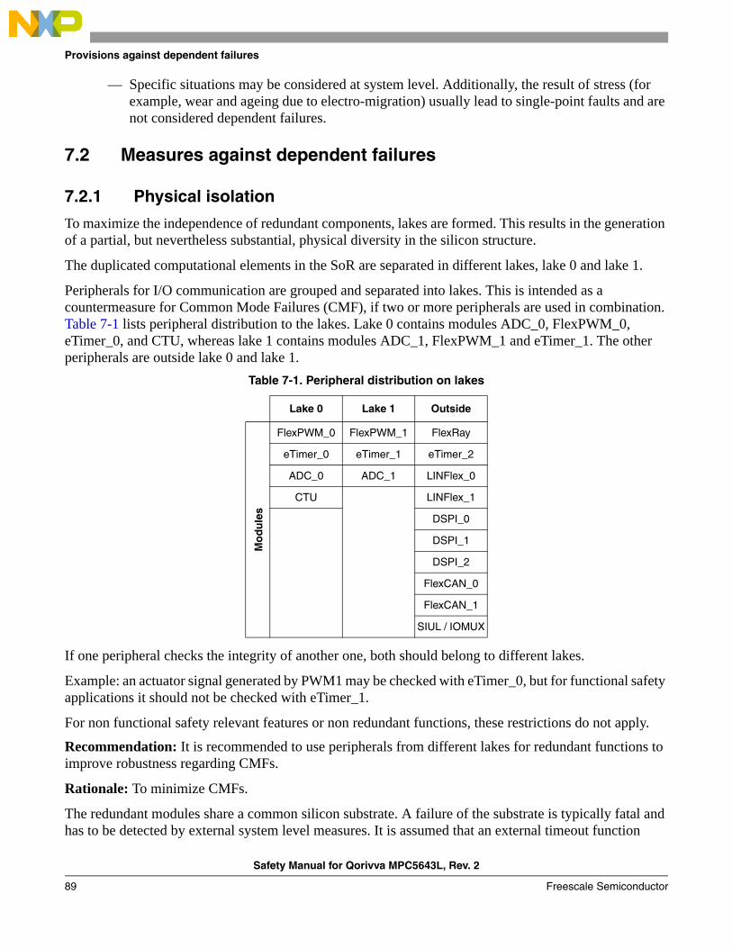
Provisions against dependent failures
— Specific situations may be considered at system level. Additionally, the result of stress (for example, wear and ageing due to electro-migration) usually lead to single-point faults and are not considered dependent failures.
7.2 Measures against dependent failures
7.2.1 Physical isolation
To maximize the independence of redundant components, lakes are formed. This results in the generation of a partial, but nevertheless substantial, physical diversity in the silicon structure.
The duplicated computational elements in the SoR are separated in different lakes, lake 0 and lake 1.
Peripherals for I/O communication are grouped and separated into lakes. This is intended as a countermeasure for Common Mode Failures (CMF), if two or more peripherals are used in combination. Table 7-1 lists peripheral distribution to the lakes. Lake 0 contains modules ADC_0, FlexPWM_0, eTimer_0, and CTU, whereas lake 1 contains modules ADC_1, FlexPWM_1 and eTimer_1. The other peripherals are outside lake 0 and lake 1.
If one peripheral checks the integrity of another one, both should belong to different lakes.
Example: an actuator signal generated by PWM1 may be checked with eTimer_0, but for functional safety applications it should not be checked with eTimer_1.
For non functional safety relevant features or non redundant functions, these restrictions do not apply.
Recommendation: It is recommended to use peripherals from different lakes for redundant functions to improve robustness regarding CMFs.
Rationale: To minimize CMFs.
The redundant modules share a common silicon substrate. A failure of the substrate is typically fatal and has to be detected by external system level measures. It is assumed that an external timeout function
Table 7-1. Peripheral distribution on lakes
Lake 0 Lake 1 Outside
Mo
du
les
FlexPWM_0 FlexPWM_1 FlexRay
eTimer_0 eTimer_1 eTimer_2
ADC_0 ADC_1 LINFlex_0
CTU LINFlex_1
DSPI_0
DSPI_1
DSPI_2
FlexCAN_0
FlexCAN_1
SIUL / IOMUX
Safety Manual for Qorivva MPC5643L, Rev. 2
Freescale Semiconductor89
Provisions against dependent failures
(watchdog) is continuously monitoring the MPC5643L and is capable of detecting this CMF, and will switch the system to a Safe statesystem within the FTTI.
The MPC5643L device satisfies the standard AECQ100 for latch-up immunity.
7.2.2 Environmental conditions
7.2.2.1 Temperature
MPC5643L was designed to work within a maximum operational temperature profile (see the Qorivva MPC5643L Microcontroller Data Sheet for details). To cover Common Mode Failures caused by temperature, sensors for supervision are implemented which are described in Section 5.2.4, Temperature Sensor (TSENS).
7.2.2.2 EMI and I/O
To cope with noise at digital inputs, the I/O circuitry provides input hysteresis on all digital inputs. Moreover, the RESET and NMI inputs contain glitch filtering capabilities, which are described in Section 5.2.24, Glitch filter.
To reduce interference due to digital outputs, the I/O circuitry provides signal slope control. An internal weak pullup or pulldown structure is also provided to define the input state.
7.2.3 Failures of common signals
7.2.3.1 Clock
To cover Common Mode Failures caused by erroneous clocks, supervisory modules are implemented as described in Section 5.2.10, Clock Monitor Unit (CMU). Major failures in the clock system are also detected by the use of the SWT (Section 5.2.5, Software Watchdog Timer (SWT)).
7.2.3.2 Power supply
To cover Common Mode Failures caused by voltage, supervisory modules are implemented as described in Section 5.2.11, Power Management Unit (PMU).
Some Common Mode Failures (for example, loss of power supply) will still be detected by the use of an external watchdog (Section 4.1.2, External Watchdog (EXWD)) because application software is no longer able to trigger the EXWD.
7.2.3.3 Non-application control signals
Modules and signals (for scan, test, and debug, for example) that are not functional safety relevant and thus have no functional safety mechanism included should never be able to violate the functional safety goal. This can be achieved by either not interfering with the functional safety relevant parts of the MPC5643L or by detecting such interference. For example, there must be assurance that the system is not debugged (or unintentionally in debug mode), or in any other special mode different from normal application
Safety Manual for Qorivva MPC5643L, Rev. 2
Freescale Semiconductor 90

Provisions against dependent failures
execution mode like test mode. FCCU failure indication is generated when one of the following conditions is fulfilled (please also refer to Table 5-1):
• The device leaves LSM.
• A self-test sequence of the STCU is unintentionally executed during normal operation of the device.
• Any of the implementations for production test are unintentionally executed during normal operation of the device.
• Any JTAGC instruction is executed that causes a system reset or Test Mode Select (TMS) signal is used to sequence the TAP controller state machine.
7.3 CMF avoidance on system levelIt is recommended that you do not use adjacent input and output signals of peripherals, which are used redundantly, to reduce CMF. As internal pad position and external pin/ball position do not necessarily correspond to each other, the system integrator may take the following recommendations into consideration:
• Usage of non-contiguous pins/balls of the package
• Usage of non-contiguous pads of the silicon
• Non-contiguous routing of these signals on the PCB
Assumption: [SM_090] It is assumed that physically adjacent signals are avoided for redundant functions.[end]
Rationale: To minimize Common Mode Failures (CMF).
Implementation hint: Pad position as well as pin/ball position should be taken into consideration.
The following section give information on which inputs use adjacent pads on the silicon.
7.3.1 I/O pin/ball configuration
For a thorough analysis of pin adjacency related to all signals, see Table 7-2. This table can be used to determine whether two pins are adjacent in the internal die for all signals and packages. Two pins, identified by the column “Port Name,” are adjacent on the internal die if the numbers in the “Physical Pad Sequence” column are consecutive (for example, pad number n and pad number n + 1 are adjacent).
Table 7-2. Physical pin displacement on internal die
Port name Pin number LQFP 144 Ball number BGA 257 Physical pad sequence1
A[0] 73 T14 94
A[1] 74 R14 96
A[2] 84 N16 106
A[3] 92 K17 118
A[4] 108 C16 145
Safety Manual for Qorivva MPC5643L, Rev. 2
Freescale Semiconductor91

Provisions against dependent failures
A[5] 14 H4 18
A[6] 2 G4 2
A[7] 10 F3 10
A[8] 12 F4 12
A[9] 134 B6 186
A[10] 118 A13 155
A[11] 120 D11 159
A[12] 122 A10 163
A[13] 136 C6 189
A[14] 143 B4 197
A[15] 144 D3 198
B[0] 109 B15 146
B[1] 110 C14 147
B[2] 114 A14 151
B[3] 116 B13 153
B[4] 89 L17 113
B[5] 86 M15 108
B[6] 138 B3 192
B[7] 43 R5 58
B[8] 47 P7 62
B[9] 52 U7 69
B[10] 53 R8 70
B[11] 54 T8 71
B[12] 55 U8 72
B[13] 60 R10 81
B[14] 64 P11 85
B[15] 62 R11 83
C[0] 66 R12 87
C[1] 41 T4 56
C[2] 45 U5 60
C[4] 11 H3 11
C[5] 13 G3 14
C[6] 142 D4 196
Table 7-2. Physical pin displacement on internal die (continued)
Port name Pin number LQFP 144 Ball number BGA 257 Physical pad sequence1
Safety Manual for Qorivva MPC5643L, Rev. 2
Freescale Semiconductor 92

Provisions against dependent failures
C[7] 15 K4 20
C[10] 111 A15 148
C[11] 80 M14 102
C[12] 82 N15 104
C[13] 101 F15 137
C[14] 103 E15 140
C[15] 124 A8 167
D[0] 125 B8 168
D[1] 3 E3 3
D[2] 140 C5 194
D[3] 128 A7 172
D[4] 129 B7 173
D[5] 33 N3 44
D[6] 34 P3 45
D[7] 37 R4 50
D[8] 32 M3 43
D[9] 26 L3 37
D[10] 76 T15 98
D[11] 78 R16 100
D[12] 99 G14 133
D[14] 105 D16 142
E[0] 68 T13 89
E[2] 49 U6 64
E[4] 42 U4 57
E[5] 44 T5 59
E[6] 46 R6 61
E[7] 48 T6 63
E[9] 61 T10 82
E[10] 63 T11 84
E[11] 65 U11 86
E[12] 67 T12 88
E[13] 117 D12 154
E[14] 119 B12 157
Table 7-2. Physical pin displacement on internal die (continued)
Port name Pin number LQFP 144 Ball number BGA 257 Physical pad sequence1
Safety Manual for Qorivva MPC5643L, Rev. 2
Freescale Semiconductor93

Provisions against dependent failures
E[15] 121 B11 161
F[0] 133 D7 180
F[10] 24 L1 35
F[11] 25 L2 36
F[12] 106 C17 143
F[13] 112 B14 149
F[14] 115 C13 152
F[15] 113 D13 150
F[3] 139 B5 193
F[4] 4 D2 4
F[5] 5 D1 5
F[6] 8 E2 8
F[7] 19 J1 29
F[8] 20 K2 30
F[9] 23 K1 34
G[2] 102 E16 139
G[3] 104 D17 141
G[4] 100 F17 135
G[5] 85 N17 107
G[6] 98 G17 131
G[7] 83 P17 105
G[8] 81 P16 103
G[9] 79 R17 101
G[10] 77 P15 99
G[11] 75 U15 97
G[12] — F2 13
G[13] — H1 21
G[14] — A6 181
G[15] — J2 28
H[0] — A5 182
H[1] — F1 15
H[2] — A4 185
H[3] — G1 19
Table 7-2. Physical pin displacement on internal die (continued)
Port name Pin number LQFP 144 Ball number BGA 257 Physical pad sequence1
Safety Manual for Qorivva MPC5643L, Rev. 2
Freescale Semiconductor 94
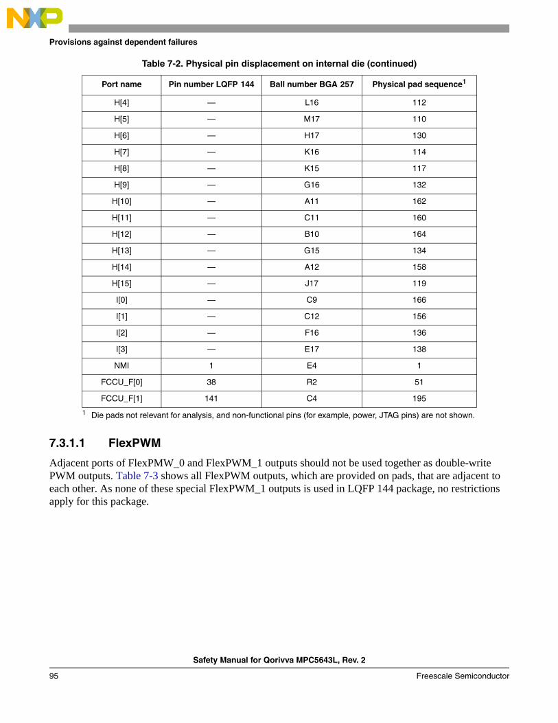
Provisions against dependent failures
7.3.1.1 FlexPWM
Adjacent ports of FlexPMW_0 and FlexPWM_1 outputs should not be used together as double-write PWM outputs. Table 7-3 shows all FlexPWM outputs, which are provided on pads, that are adjacent to each other. As none of these special FlexPWM_1 outputs is used in LQFP 144 package, no restrictions apply for this package.
H[4] — L16 112
H[5] — M17 110
H[6] — H17 130
H[7] — K16 114
H[8] — K15 117
H[9] — G16 132
H[10] — A11 162
H[11] — C11 160
H[12] — B10 164
H[13] — G15 134
H[14] — A12 158
H[15] — J17 119
I[0] — C9 166
I[1] — C12 156
I[2] — F16 136
I[3] — E17 138
NMI 1 E4 1
FCCU_F[0] 38 R2 51
FCCU_F[1] 141 C4 195
1 Die pads not relevant for analysis, and non-functional pins (for example, power, JTAG pins) are not shown.
Table 7-2. Physical pin displacement on internal die (continued)
Port name Pin number LQFP 144 Ball number BGA 257 Physical pad sequence1
Safety Manual for Qorivva MPC5643L, Rev. 2
Freescale Semiconductor95
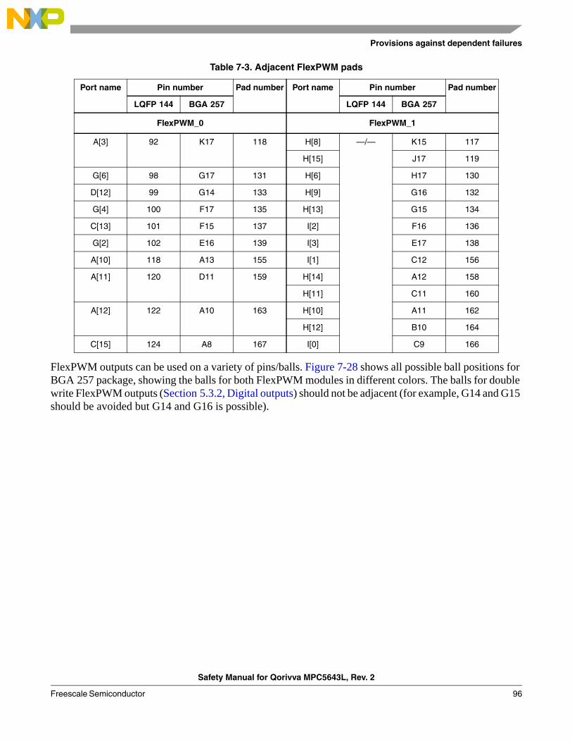
Provisions against dependent failures
FlexPWM outputs can be used on a variety of pins/balls. Figure 7-28 shows all possible ball positions for BGA 257 package, showing the balls for both FlexPWM modules in different colors. The balls for double write FlexPWM outputs (Section 5.3.2, Digital outputs) should not be adjacent (for example, G14 and G15 should be avoided but G14 and G16 is possible).
Table 7-3. Adjacent FlexPWM pads
Port name Pin number Pad number Port name Pin number Pad number
LQFP 144 BGA 257 LQFP 144 BGA 257
FlexPWM_0 FlexPWM_1
A[3] 92 K17 118 H[8] —/— K15 117
H[15] J17 119
G[6] 98 G17 131 H[6] H17 130
H[9] G16 132D[12] 99 G14 133
H[13] G15 134G[4] 100 F17 135
I[2] F16 136C[13] 101 F15 137
I[3] E17 138G[2] 102 E16 139
A[10] 118 A13 155 I[1] C12 156
A[11] 120 D11 159 H[14] A12 158
H[11] C11 160
A[12] 122 A10 163 H[10] A11 162
H[12] B10 164
C[15] 124 A8 167 I[0] C9 166
Safety Manual for Qorivva MPC5643L, Rev. 2
Freescale Semiconductor 96

Provisions against dependent failures
Figure 7-28. FlexPWM balls (BGA 257)
7.3.1.2 eTimer
The following Ports of eTimer_0, eTimer_1, and eTimer_2 outputs should not be used together (for example, as double-read PWM inputs or double-read encoder inputs).
Safety Manual for Qorivva MPC5643L, Rev. 2
Freescale Semiconductor97
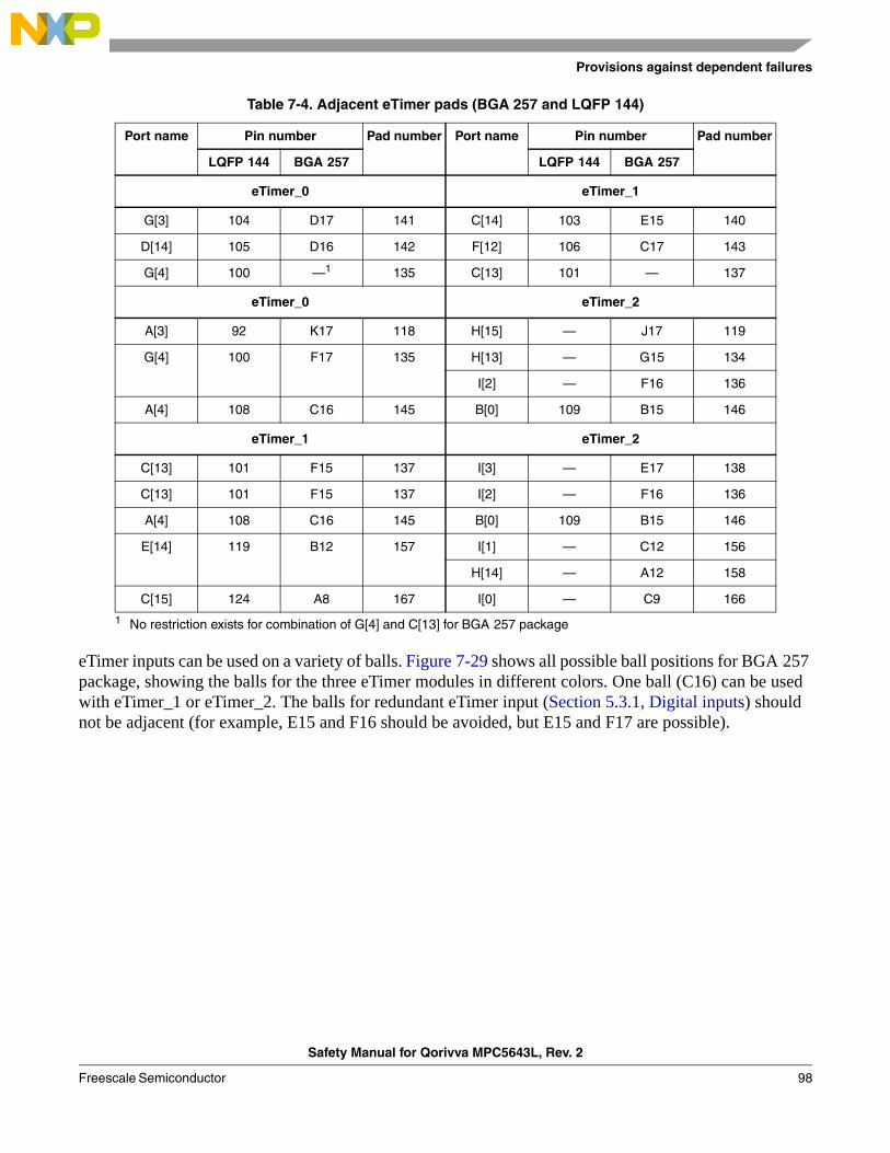
Provisions against dependent failures
eTimer inputs can be used on a variety of balls. Figure 7-29 shows all possible ball positions for BGA 257 package, showing the balls for the three eTimer modules in different colors. One ball (C16) can be used with eTimer_1 or eTimer_2. The balls for redundant eTimer input (Section 5.3.1, Digital inputs) should not be adjacent (for example, E15 and F16 should be avoided, but E15 and F17 are possible).
Table 7-4. Adjacent eTimer pads (BGA 257 and LQFP 144)
Port name Pin number Pad number Port name Pin number Pad number
LQFP 144 BGA 257 LQFP 144 BGA 257
eTimer_0 eTimer_1
G[3] 104 D17 141 C[14] 103 E15 140
D[14] 105 D16 142 F[12] 106 C17 143
G[4] 100 —1
1 No restriction exists for combination of G[4] and C[13] for BGA 257 package
135 C[13] 101 — 137
eTimer_0 eTimer_2
A[3] 92 K17 118 H[15] — J17 119
G[4] 100 F17 135 H[13] — G15 134
I[2] — F16 136
A[4] 108 C16 145 B[0] 109 B15 146
eTimer_1 eTimer_2
C[13] 101 F15 137 I[3] — E17 138
C[13] 101 F15 137 I[2] — F16 136
A[4] 108 C16 145 B[0] 109 B15 146
E[14] 119 B12 157 I[1] — C12 156
H[14] — A12 158
C[15] 124 A8 167 I[0] — C9 166
Safety Manual for Qorivva MPC5643L, Rev. 2
Freescale Semiconductor 98
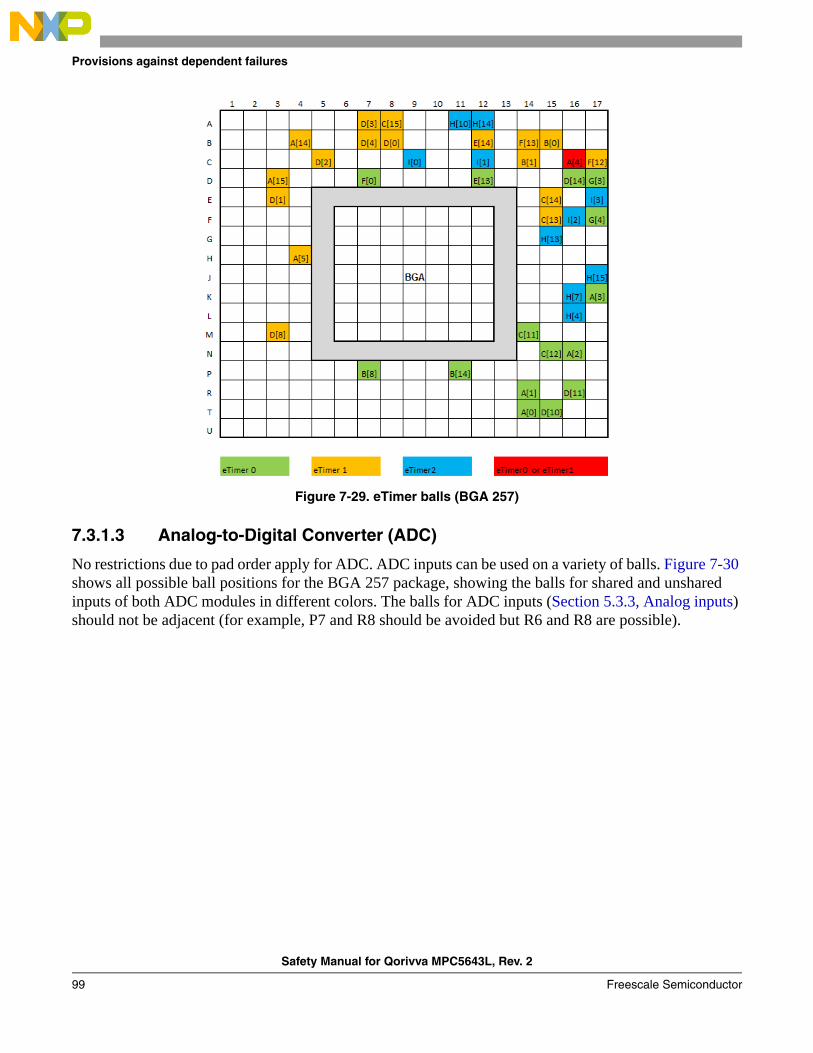
Provisions against dependent failures
Figure 7-29. eTimer balls (BGA 257)
7.3.1.3 Analog-to-Digital Converter (ADC)
No restrictions due to pad order apply for ADC. ADC inputs can be used on a variety of balls. Figure 7-30 shows all possible ball positions for the BGA 257 package, showing the balls for shared and unshared inputs of both ADC modules in different colors. The balls for ADC inputs (Section 5.3.3, Analog inputs) should not be adjacent (for example, P7 and R8 should be avoided but R6 and R8 are possible).
Safety Manual for Qorivva MPC5643L, Rev. 2
Freescale Semiconductor99
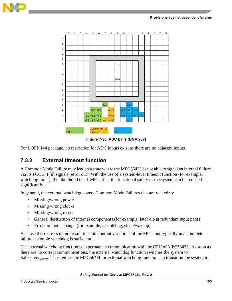
Provisions against dependent failures
Figure 7-30. ADC balls (BGA 257)
For LQFP 144 package, no restriction for ADC inputs exist as there are no adjacent inputs.
7.3.2 External timeout function
A Common Mode Failure may lead to a state where the MPC5643L is not able to signal an internal failure via its FCCU_F[n] signals (error out). With the use of a system-level timeout function (for example, watchdog timer), the likelihood that CMFs affect the functional safety of the system can be reduced significantly.
In general, the external watchdog covers Common Mode Failures that are related to:
• Missing/wrong power
• Missing/wrong clocks
• Missing/wrong resets
• General destruction of internal components (for example, latch-up at redundant input pads)
• Errors in mode change (for example, test, debug, sleep/wakeup)
Because these errors do not result in subtle output variations of the MCU but typically in a complete failure, a simple watchdog is sufficient.
The external watchdog function is in permanent communication with the CPU of MPC5643L. As soon as there are no correct communications, the external watchdog function switches the system to Safe statesystem. Thus, either the MPC5643L or external watchdog function can transition the system to
Safety Manual for Qorivva MPC5643L, Rev. 2
Freescale Semiconductor 100

Provisions against dependent failures
Safe statesystem. The external watchdog function is required to be sufficiently independent of the MPC5643L (for example, regarding clock generation, power supply, and so on).
The external watchdog function does not necessarily need to be a dedicated IC; the requirements may also be fulfilled by another MCU (already used in the system) that is capable of detecting a communication problem and moving the system to Safe statesystem.
7.4 IC considerationsAccording to IEC 61508 and ISO 26262, the susceptibility of the IC with on-chip redundancy to Common Mode Failures shall be estimated.
This is done by determining the -factor IC defined in annex E of IEC 61508-2. The IC is calculated based on a bonus-malus system. The smaller the IC, the less susceptible the IC is to Common Mode Failures. The estimated final IC should not exceed 25%; otherwise, additional measures might be required. Refer to the IC calculation results which are part of the FMEDA document.
As ISO 26262 does not specify a method to quantify Common Mode Failures, the results of the IC analysis may be used as indication for ISO 26262 as well.
Safety Manual for Qorivva MPC5643L, Rev. 2
Freescale Semiconductor101

Additional information
8 Additional information
8.1 Safety function pseudo-codeCAUTION
For some functions, code examples are given to exemplify the intended functionality and give some hints on integration. This code does not cover all aspects of actual applications and, as such, is intended to be used as a general guideline.
In some code examples given in this chapter, “while” loops are used. These loops may never terminate, depending on their condition. To prevent termination of software execution flow, a timeout function may be implemented (see Figure 8-31). For simplicity, such a timeout is not used in the code examples for the safety integrity functions, but may be used in system level application software.
Figure 8-31. Code example: timeout
start_time = read_timer();do current_time = read_timer() - start_time; while ((Current_time < Limit) && (Flag_not_set))if (Flag_set)
PASS;else
FAIL;
Safety Manual for Qorivva MPC5643L, Rev. 2
Freescale Semiconductor 102

Additional information
8.1.1 Flash memory
8.1.1.1 FLASH_SW_ECCTEST
Figure 8-32. Code example: FLASH_SW_ECCTEST (definitions)
definitions for FLASH_SW_ECCTEST
#define C90FL_BASE 0xC3F88000#define C90FL_MCR (*(vuint32_t *)(C90FL_BASE))#define C90FL_ADR (*(vuint32_t *)(C90FL_BASE+0x18))#define C90FL_UT0 (*(vuint32_t *)(C90FL_BASE+0x3C))#define C90FL_UT1 (*(vuint32_t *)(C90FL_BASE+0x40))#define C90FL_UT2 (*(vuint32_t *)(C90FL_BASE+0x44))
#define C90FL_UT_PASSWORD 0xF9F99999
#define UT0_UTE (0x80000000)#define UT0_SBCE (0x40000000)#define UT0_DSI(x) (((x)&0xFF)<<16)#define UT0_EIE (0x00000008) #define UT0_AIS (0x00000004) #define UT0_AIE (0x00000002) #define UT0_AID (0x00000001)
#define MCR_SBC (0x00002000)
#define C90FL_OK 0x0#define C90FL_ECC_DECODE_FAIL 0xE
#define ReadAddrLong(addr) (*((vuint32_t *) (addr)))#define RegFieldSet(preg, bit, value) preg &=
~bit(0xFFFFFFFF); preg |= bit(value)
// Bit definitions and macros for // C90FL_UT0
// Data syndrome input// ECC data input enable// Array integrity sequence// Array integrity enable// Array integrity done
// return code ECC decode test pass// return code ECC decode test fail
// macros for reading/setting registers // or addresses
Safety Manual for Qorivva MPC5643L, Rev. 2
Freescale Semiconductor103
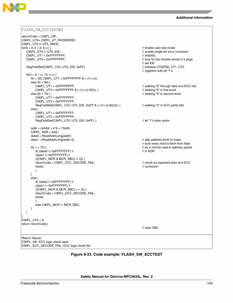
Additional information
Figure 8-33. Code example: FLASH_SW_ECCTEST
FLASH_SW_ECCTEST() {
returnCode = C90FL_OK;C90FL_UT0= C90FL_UT_PASSWORD;C90FL_UT0 |= UT0_SBCE;for(k = 0; k < 2; k++) {
C90FL_UT0 |= UT0_EIE; C90FL_UT1 = 0xFFFFFFFF;C90FL_UT2 = 0xFFFFFFFF;
RegFieldSet(C90FL_UT0, UT0_DSI, 0xFF);
for(i = 0; i <= 72; i++) {if(i < 32) C90FL_UT1 = 0xFFFFFFFF & (~(1<<i));else if(i < 64) {
C90FL_UT1 = 0xFFFFFFFF;C90FL_UT2 = 0xFFFFFFFF & (~(1<<(i-32))); }
else if(i < 72) {C90FL_UT1 = 0xFFFFFFFF;C90FL_UT2 = 0xFFFFFFFF;RegFieldSet(C90FL_UT0, UT0_DSI, (0xFF & (~(1<<(i-64))))); }
else {C90FL_UT1 = 0xFFFFFFFF;C90FL_UT2 = 0xFFFFFFFF;RegFieldSet(C90FL_UT0, UT0_DSI, 0xFF); }
addr = rdAddr + k*8 + i*0x40; C90FL_ADR = addr; data0 = ReadAddrLong(addr);data1 = ReadAddrLong(addr+4);
if(i = = 72) {if( (data0 != 0xFFFFFFFF) || (data1 != 0xFFFFFFFF) || ((C90FL_MCR & MCR_SBC) != 0)) {returnCode = C90FL_ECC_DECODE_FAIL; break;}
}else {
if( (data0 != 0xFFFFFFFF) || (data1 != 0xFFFFFFFF) || ((C90FL_MCR & MCR_SBC) = = 0)) {returnCode = C90FL_ECC_DECODE_FAIL; break;}else C90FL_MCR |= MCR_SBC;
}}
}C90FL_UT0 = 0;return returnCode;}
// enable user-test mode// enable single-bit error correction // visibility// loop for two double-words in a page// set EIE// Initialize UT0[DSI], UT1, UT2 // registers with all “1”s
// walking “0” through data and ECC bits// walking “0” in first word// walking “0” in second word
// walking “0” in ECC parity bits
// all “1”s data vector
// skip address 0x40 to make // sure every read is fetch from flash// do a normal read to address saved // in ADR
// check for expected data and ECC // correction
// clear SBC
Return Values:C90FL_OK: ECC logic check passC90FL_ECC_DECODE_FAIL: ECC logic check fail
Safety Manual for Qorivva MPC5643L, Rev. 2
Freescale Semiconductor 104
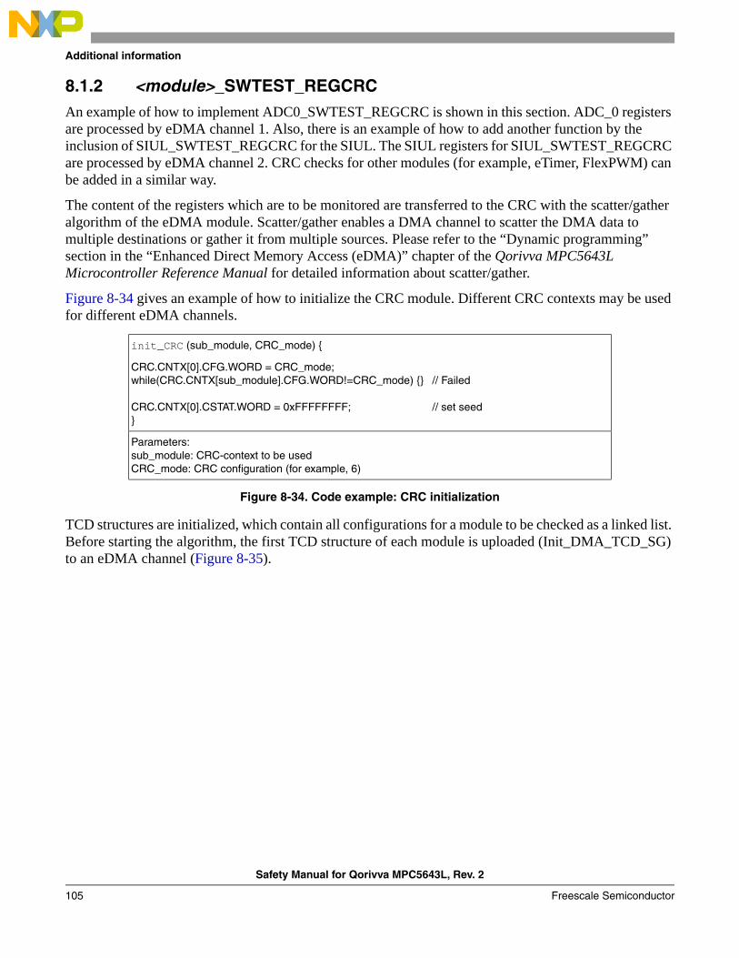
Additional information
8.1.2 <module>_SWTEST_REGCRCAn example of how to implement ADC0_SWTEST_REGCRC is shown in this section. ADC_0 registers are processed by eDMA channel 1. Also, there is an example of how to add another function by the inclusion of SIUL_SWTEST_REGCRC for the SIUL. The SIUL registers for SIUL_SWTEST_REGCRC are processed by eDMA channel 2. CRC checks for other modules (for example, eTimer, FlexPWM) can be added in a similar way.
The content of the registers which are to be monitored are transferred to the CRC with the scatter/gather algorithm of the eDMA module. Scatter/gather enables a DMA channel to scatter the DMA data to multiple destinations or gather it from multiple sources. Please refer to the “Dynamic programming” section in the “Enhanced Direct Memory Access (eDMA)” chapter of the Qorivva MPC5643L Microcontroller Reference Manual for detailed information about scatter/gather.
Figure 8-34 gives an example of how to initialize the CRC module. Different CRC contexts may be used for different eDMA channels.
Figure 8-34. Code example: CRC initialization
TCD structures are initialized, which contain all configurations for a module to be checked as a linked list. Before starting the algorithm, the first TCD structure of each module is uploaded (Init_DMA_TCD_SG) to an eDMA channel (Figure 8-35).
init_CRC (sub_module, CRC_mode) {
CRC.CNTX[0].CFG.WORD = CRC_mode;while(CRC.CNTX[sub_module].CFG.WORD!=CRC_mode) {}
CRC.CNTX[0].CSTAT.WORD = 0xFFFFFFFF;}
// Failed
// set seed
Parameters:sub_module: CRC-context to be usedCRC_mode: CRC configuration (for example, 6)
Safety Manual for Qorivva MPC5643L, Rev. 2
Freescale Semiconductor105
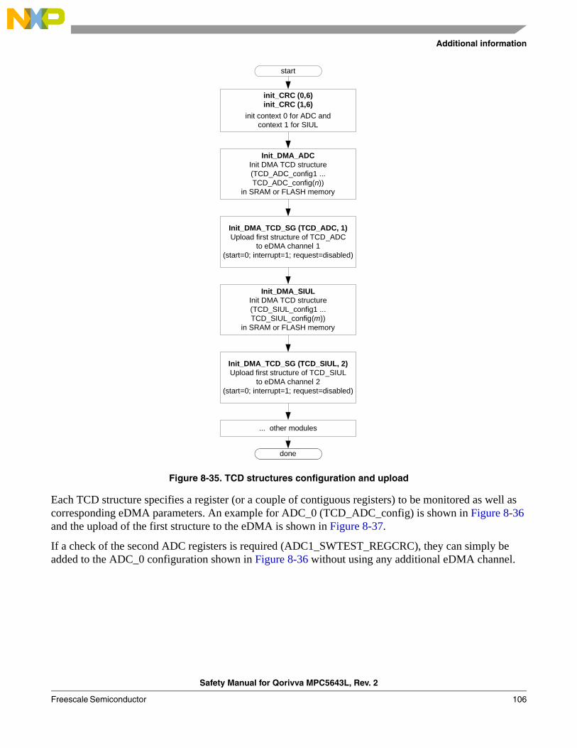
Additional information
Figure 8-35. TCD structures configuration and upload
Each TCD structure specifies a register (or a couple of contiguous registers) to be monitored as well as corresponding eDMA parameters. An example for ADC_0 (TCD_ADC_config) is shown in Figure 8-36 and the upload of the first structure to the eDMA is shown in Figure 8-37.
If a check of the second ADC registers is required (ADC1_SWTEST_REGCRC), they can simply be added to the ADC_0 configuration shown in Figure 8-36 without using any additional eDMA channel.
start
Init_DMA_ADCInit DMA TCD structure (TCD_ADC_config1 ... TCD_ADC_config(n))
in SRAM or FLASH memory
Init_DMA_TCD_SG (TCD_ADC, 1)Upload first structure of TCD_ADC
to eDMA channel 1(start=0; interrupt=1; request=disabled)
done
Init_DMA_SIULInit DMA TCD structure (TCD_SIUL_config1 ... TCD_SIUL_config(m))
in SRAM or FLASH memory
Init_DMA_TCD_SG (TCD_SIUL, 2)Upload first structure of TCD_SIUL
to eDMA channel 2(start=0; interrupt=1; request=disabled)
... other modules
init_CRC (0,6)init_CRC (1,6)
init context 0 for ADC and context 1 for SIUL
Safety Manual for Qorivva MPC5643L, Rev. 2
Freescale Semiconductor 106

Additional information
Figure 8-36. Code example: TCD_ADC configuration in SRAM
Init_DMA_ADC (){
TCD_ADC_config1.sadr = & ADC0.IMR.R;TCD_ADC_config1.smod = 0;TCD_ADC_config1.ssize= 2;TCD_ADC_config1.dmod= 0;TCD_ADC_config1.dsize= 2;TCD_ADC_config1.soff= 4;TCD_ADC_config1.nbytes= 8;TCD_ADC_config1.slast= 0; TCD_ADC_config1.dadr=& CRC.CNTX[0].INP.R;TCD_ADC_config1.citer_e_link= 0; TCD_ADC_config1.citer_linkch= 0;TCD_ADC_config1.citer= 1; TCD_ADC_config1.doff= 0;TCD_ADC_config1.dlast_sga=&TCD_ADC_config2;TCD_ADC_config1.biter_e_link= 0; TCD_ADC_config1.biter_linkch= 0;TCD_ADC_config1.biter= 1; TCD_ADC_config1.bwc= 0; TCD_ADC_config1.major_linkch= 0;TCD_ADC_config1.done= 0; TCD_ADC_config1.active= 0; TCD_ADC_config1.major_e_link= 0;TCD_ADC_config1.e_sg= 1;TCD_ADC_config1.d_req= 0;TCD_ADC_config1.int_half= 0; TCD_ADC_config1.int_maj= 0; TCD_ADC_config1.start= 0;TCD_ADC_config1.smloe= 0;TCD_ADC_config1.dmloe= 0;TCD_ADC_config1.mmloff= 0;
TCD_ADC_config2.sadr= & ADC0.WTISR.R;TCD_ADC_config2.dlast_sga= &TCD_ADC_config3; TCD_ADC_config2.d_req= 0;TCD_ADC_config2.int_maj= 0; TCD_ADC_config2.start= 1;TCD_ADC_config2.smloe= 0;[all other TCD elements]
TCD_ADC_config(n).sadr= & ADC0.DMAE.R;TCD_ADC_confign(n).dlast_sga= &TCD_ADC_config1; TCD_ADC_confign(n).d_req= 1;TCD_ADC_confign(n).int_maj= 1; TCD_ADC_confign(n).start= 1;TCD_ADC_confign(n).smloe= 0;[all other TCD elements]}
// ADC_0 - IMR & CIMR0// source address modulo// source data transfer size// destination address Module// destination data transfer size// source address signed offset// inner minor byte transfer count// last source address adjustment// destination address = input of CRC// context 0// enable c2c linking (minor loop compl.)// link channel number// current major iteration count// destination address signed offset
// enable c2c linking (minor loop compl.)// bandwidth control// link channel number// channel done// channel active// enable c2c linking (major loop compl.)// enable scatter/gather processing// disable request// enable interrupt (major count)// enable interrupt (major iteration)// channel start
// ADC_0 - WTISR & WTIMR
// ADC_0 - DMAE & DMAR0
Safety Manual for Qorivva MPC5643L, Rev. 2
Freescale Semiconductor107

Additional information
Figure 8-37. Code example: first structure upload to eDMA
Figure 8-38 shows the execution flow of the eDMA modules scatter/gather algorithm. Once the first channel is started by setting DMASERQ = 1, all structures (TCD_ADC_config) are executed consecutively. An interrupt is issued after the last eDMA transfer has been finished (for example, TCD_ADC_config(n) in Figure 8-38). Then the calculated CRC value for all TCD_ADC_config1…TCD_ADC_config(n) can be compared to the expected (predetermined) CRC value. All channels used for a <module>_SWTEST_REGCRC are repetitively started (DMASERQ) according to the required frequency (for example, only once or once in the FTTI).
Init_DMA_TCD_SG (T, channel){
DMA_CH_MUX.CHCONFIG[channel].B.SOURCE = 28;DMA_CH_MUX.CHCONFIG[channel].B.TRIG = 0;DMA_CH_MUX.CHCONFIG[channel].B.ENBL = 1;
SPP_DMA2.CHANNEL[channel].TCDWORD0_.B.SADDR = T.sadr;SPP_DMA2.CHANNEL[channel].TCDWORD16_.B.DADDR = T.dadr;SPP_DMA2.CHANNEL[channel].TCDWORD4_.B.SMOD = T.smod;SPP_DMA2.CHANNEL[channel].TCDWORD4_.B.DMOD = T.dmod;SPP_DMA2.CHANNEL[channel].TCDWORD4_.B.DSIZE = T.dsize;SPP_DMA2.CHANNEL[channel].TCDWORD4_.B.SSIZE = T.ssize;SPP_DMA2.CHANNEL[channel].TCDWORD4_.B.SOFF = T.soff;SPP_DMA2.CHANNEL[channel].TCDWORD20_.B.DOFF = T.doff;SPP_DMA2.CHANNEL[channel].TCDWORD12_.B.SLAST = T.slast;[]}
// add all other
Parameters:T: TCD structureschannel: eDMA channel
Safety Manual for Qorivva MPC5643L, Rev. 2
Freescale Semiconductor 108
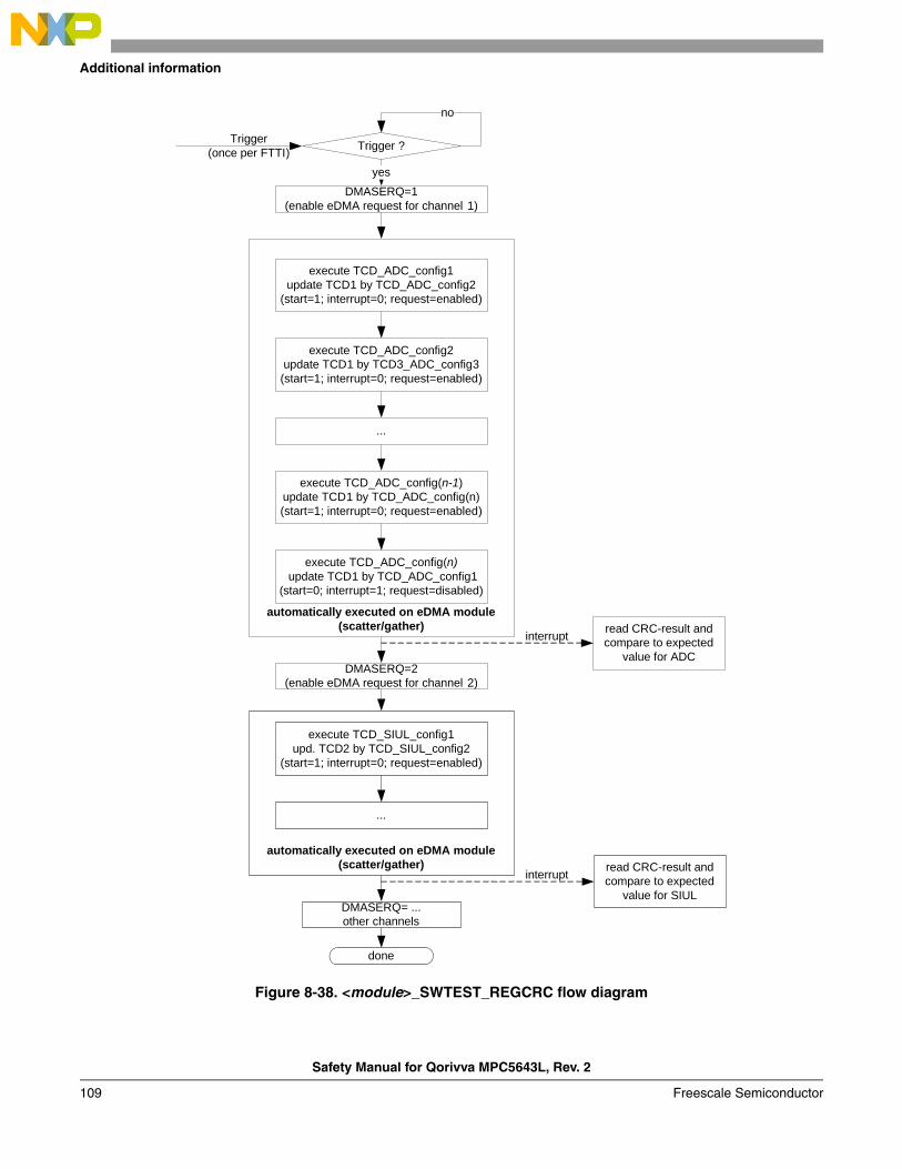
Additional information
Figure 8-38. <module>_SWTEST_REGCRC flow diagram
DMASERQ=1(enable eDMA request for channel 1)
Trigger ?
yes
no
DMASERQ=2(enable eDMA request for channel 2)
automatically executed on eDMA module(scatter/gather)
done
automatically executed on eDMA module(scatter/gather)
execute TCD_ADC_config1update TCD1 by TCD_ADC_config2
(start=1; interrupt=0; request=enabled)
execute TCD_ADC_config2update TCD1 by TCD3_ADC_config3(start=1; interrupt=0; request=enabled)
...
execute TCD_ADC_config(n) update TCD1 by TCD_ADC_config1
(start=0; interrupt=1; request=disabled)
execute TCD_ADC_config(n-1)update TCD1 by TCD_ADC_config(n)(start=1; interrupt=0; request=enabled)
execute TCD_SIUL_config1upd. TCD2 by TCD_SIUL_config2
(start=1; interrupt=0; request=enabled)
...
DMASERQ= ...other channels
Trigger(once per FTTI)
interruptread CRC-result andcompare to expected
value for ADC
read CRC-result andcompare to expected
value for SIUL
interrupt
Safety Manual for Qorivva MPC5643L, Rev. 2
Freescale Semiconductor109

Additional information
8.1.3 CTU
Figure 8-39. Code example: CTU initialization
Init_CTU(trig, mode) {
if (trig <= 3) {if (mode) {
CTU.THCR1.R |= (1 << ((trig*8)+1)); }else {
CTU.THCR1.R &= ~(1 << ((trig*8)+1)); }}
else {trig -= 4;if (mode) {
CTU.THCR2.R |= (1 << ((trig*8)+1)); }else {
CTU.THCR2.R &= ~(1 << ((trig*8)+1));}
}
CTU.TGSCRR.R = 0x10;CTU.TGSCCR.R = 0x100;
CTU.CTUCR.B.GRE = 1;CTU.CTUCR.B.MRS_SG = 1;
CTU.CTUEFR.R |= 0x0400;
dummy = CTU.CTUIFR.R;dummy = CTU.CTUEFR.R;CTU.CTUIR.B.IEE = 1;}
// enable eTimer_0 output
// disable eTimer_0 output
// enable eTimer_0 output
// enable eTimer_0 output
// set some BS value to avoid compare error
// set Global Reload// load new configuration into CTU
// clear the CMP_ERR bit (??)
// clear any pending interrupts
// enable error interrupts (CTU reports overruns via// interrupts)
Parameterstrig: selects the trigger to be linked to the timermode: controls the SET/CLEAR of the selected trigger
Safety Manual for Qorivva MPC5643L, Rev. 2
Freescale Semiconductor 110

Additional information
8.1.3.1 CTU_HWSWTEST_ADCCOMMAND
Figure 8-40. Code example: CTU_HWSWTEST_ADCCOMMAND
8.1.3.2 CTU_SWTEST_ETIMERCOMMAND
An example configuration for implementing the CTU_SWTEST_ETIMERCOMMAND is shown in Figure 8-41. Channel 2 of eTimer_0 generates the Master Reload Signal (MRS) for the CTU. Based on this signal, the CTU generates eight output triggers in triggered mode. These are counted by channel 0 of eTimer_0. With every interrupt from channel 2 of eTimer_0 occurring with a new MRS, the counter register (CNTR) of channel 0 can be verified for accuracy.
CTU_HWSWTEST_ADCCOMMAND (){
{[#define ADC_NUMBER 4;]
ADC_seq[ADC_NUMBER] = {11, 12, 13, 14};temp[2*ADC_NUMBER] = {0,0,0,0,0,0,0,0};
CTU.CTUCR.B.MRS_SG = 1;
while (!(ADC0.CDR[ADC_seq[ADC_NUMBER-1]].B.VALID));
for (i = 0; i<(ADC_NUMBER*2); i++) {switch (i/2) {
case 0:temp[i] = CTU_0.FR0.R;break;case 1:temp[i] = CTU_0.FR1.R;break;case 2:temp[i] = CTU_0.FR2.R;break;case 3:temp[i] = CTU_0.FR3.R;break;
}}
for (i = 0; i<ADC_NUMBER*2; i++) {if (ADC_seq[i/2] != ((temp[i]>>16)&0xF)) return FAIL;if (((temp[i]>>20)&0x1)==(i%2)) return FAIL;
}return PASS;}
// number of test channels - max 24
// channels of ADC to be measured// data from CTU FIFO memory
// start
// check channels and ADCs// ADC_0 has value “1” and ADC_1 // has value ‘0’ in FIFO memory!
Return Values:PASS: ADC number and channel number are correctFAIL: otherwise
Safety Manual for Qorivva MPC5643L, Rev. 2
Freescale Semiconductor111

Additional information
Figure 8-41. Configuration for sequential mode example
Figure 8-42. Code example: CTU initialization
void Init_CTU(uint16_t period,uint8_t nof){
CTU.TGSCR.B.PRES = 0x3;CTU.TGSCR.B.MRS_SM = 26;CTU.TGSCRR.R = 0x0;CTU.TGSCCR.R = 0x7FFF;
if (period < 9) CTU.COTR.R = 30*period;else CTU.COTR.R = 0xFF;
CTU.CTUCR.B.T0_SG = 0x0;
if (period>273) period = 273*30;else period*=30;
if (nof>=1){CTU.T0CR.R = period;CTU.THCR1.B.T0_E = 0x1;CTU.THCR1.B.T0_ETE = 0x1;CTU.THCR1.B.T0_T1E = 0x1;
}[… trigger 1 to 7]
if (nof>=8){CTU.T7CR.R = 8*period;CTU.THCR2.B.T7_E = 0x1;CTU.THCR2.B.T7_ETE = 0x1;CTU.THCR2.B.T7_T1E = 0x1;
}
CTU.TGSISR.B.I13_RE = 0x1;CTU.CTUCR.B.TGSISR_RE = 0x1;CTU.CTUCR.B.GRE = 0x1;CTU.CTUIR.B.MRS_IE = 0x1;
CTU.CTUIR.B.IEE = 1;}
// Configure TGS counter - prescaler 4// MRS signal from eTimer_0 [2]
//always 1/4 total period, max. 2.125 s
// keep value inside 16-bit range of// trigger compare registers
//configuration scheduler unit
//allow external signal for MRS - eTimer_0 [2]//reload global setting
//enable error interrupts
Parametersperiod: period of trigger to be generatednof: number of trigger to be generated
CTU
eTimer0_0 eTimer0_2
clk/64pri pri
eTimer0_trig eTimer0_in
number of triggers
MRSCTU_OUT
Safety Manual for Qorivva MPC5643L, Rev. 2
Freescale Semiconductor 112

Additional information
Figure 8-43. Code example: eTimer initialization
Init_Etimer(period,nof) {
ETIMER_0.ENBL.R = 0;
ETIMER_0.CHANNEL[0].COMP1.R = 0x0;ETIMER_0.CHANNEL[0].COMP2.R = 0x0;ETIMER_0.CHANNEL[0].LOAD.R = 0x0;
ETIMER_0.CHANNEL[0].CTRL.B.CNTMODE = 0x1; ETIMER_0.CHANNEL[0].CTRL.B.PRISRC = 0x8; ETIMER_0.CHANNEL[0].CTRL.B.SECSRC = 0x6;ETIMER_0.CHANNEL[0].CTRL.B.LENGTH = 0x0;ETIMER_0.CHANNEL[0].CTRL2.R = 0x0;
ETIMER_0.CHANNEL[0].INTDMA.R = 0x0;ETIMER_0.CHANNEL[0].CMPLD1.R = 0x0;ETIMER_0.CHANNEL[0].CMPLD2.R = 0x0;ETIMER_0.CHANNEL[0].FILT.R = 0x0;
ETIMER_0.ENBL.R |= (1<<0);
ETIMER_0.CHANNEL[2].COMP1.R = 2*(nof*period+2);ETIMER_0.CHANNEL[2].COMP2.R = 2*(nof*period+2)+0xA;
ETIMER_0.CHANNEL[2].LOAD.R = 0x0;
ETIMER_0.CHANNEL[2].CTRL.B.CNTMODE = 0x1;ETIMER_0.CHANNEL[2].CTRL.B.PRISRC = 0x1E;ETIMER_0.CHANNEL[2].CTRL.B.SECSRC = 0x6;ETIMER_0.CHANNEL[2].CTRL.B.LENGTH = 0x1;
ETIMER_0.CHANNEL[2].CTRL2.B.OEN = 0x1;ETIMER_0.CHANNEL[2].CTRL2.B.OUTMODE = 0x8;
ETIMER_0.CHANNEL[2].CCCTRL.B.CLC2 = 0x7;ETIMER_0.CHANNEL[2].CCCTRL.B.CPT2MODE = 0x0;ETIMER_0.CHANNEL[2].CCCTRL.B.CPT1MODE = 0x0;ETIMER_0.CHANNEL[2].CCCTRL.B.CFWM = 0x0;ETIMER_0.CHANNEL[2].CCCTRL.B.ARM = 0x0;
ETIMER_0.CHANNEL[2].INTDMA.R = 0x0;ETIMER_0.CHANNEL[2].CMPLD1.R = 0x0;ETIMER_0.CHANNEL[2].CMPLD2.R = 0x0;ETIMER_0.CHANNEL[2].FILT.R = 0x0;
ETIMER_0.ENBL.R |= (1<<2);}
//stop all channels
// set compare and load values to zero
// count rising edges of primary source// primary source IPB 1:1 and capturing on rising// edge of secondary source (output CTU)
// disable DMA, interrupts, input filter, etc.
// enable eTimer channel
// delay between MRS pulses// 2*(nof*period+2) approximately 120/64*(nof*period+2)// 2 - is reserve between two pulses MRS for checking// numbers of triggers events// 120/64 - it is period of input signal (primary source) of // eTimer_0 [2]// 0xA = width of MRS signal// Count rising edges of primary source// primary source IPB 1:1 and capturing on rising// edge of secondary source (output CTU)
// disable DMA, interrupts, input filter, etc.
// enable eTimer channel
Parametersperiod: period of trigger to be generatednof: number of trigger to be generated
Safety Manual for Qorivva MPC5643L, Rev. 2
Freescale Semiconductor113

Additional information
8.1.3.3 CTU_HWSWTEST_TRIGGEROVERRUN
Figure 8-44. Code example: CTU_HWSWTEST_TRIGGEROVERRUN
8.1.3.4 CTU_SWTEST_TRIGGERTIME (sequential mode)
An example configuration for implementing the CTU_SWTEST_TRIGGERTIME for eight triggers in sequential mode is shown in Figure 8-45. Channel 2 of eTimer_0 generates an Event Signal (EV) for the CTU. Channel 2 of eTimer_1 generates the MRS for the CTU. Based on these signals, the CTU generates the desired delayed output signal (CTU_OUT). In this example, the delay is configured to increase with every event signal (defined in CTU initialization shown in Figure 8-45). Channel 0 of eTimer_0 drives a signal which is high during the delay caused by the CTU (from rising edge of EV to rising edge of CTU_OUT). Channel 1 of eTimer_0 measures the delay which can then be checked for accuracy.
Figure 8-45. Configuration for sequential mode example
CTU_HWSWTEST_TRIGGEROVERRUN (* store_var){
temp = (*store_var & 0x0BE0);
if (temp) {return (FAIL);}
return (PASS);}
// mask all errors except external trigger, // timer N triggers and ADC command // overrun
// if there are any, this is a error // error detected, thus FAIL
Parameters*store_var: When the CTUEFR register is read, it's content is cleared. The original content is stored in address give by store_var
Return Values:PASS: no overrunFAIL: otherwise
CTU
eTimer0_0
eTimer0_1
eTimer0_2
eTimer1_2
clk/32
clk
pri
sec
pri
pri
eTimer0_trig
pri
sec
eTimer1_in
eTimer0_in
delay
MRS
EVCTU_OUT
DIFF
Safety Manual for Qorivva MPC5643L, Rev. 2
Freescale Semiconductor 114

Additional information
Figure 8-46 shows a timing example of this configuration.
Figure 8-46. Timing for sequential mode example
Example code for eTimers and CTU is shown in Figure 8-47, Figure 8-48, and Figure 8-49.
EV
MRS
CTU_OUT
DIFF
Safety Manual for Qorivva MPC5643L, Rev. 2
Freescale Semiconductor115
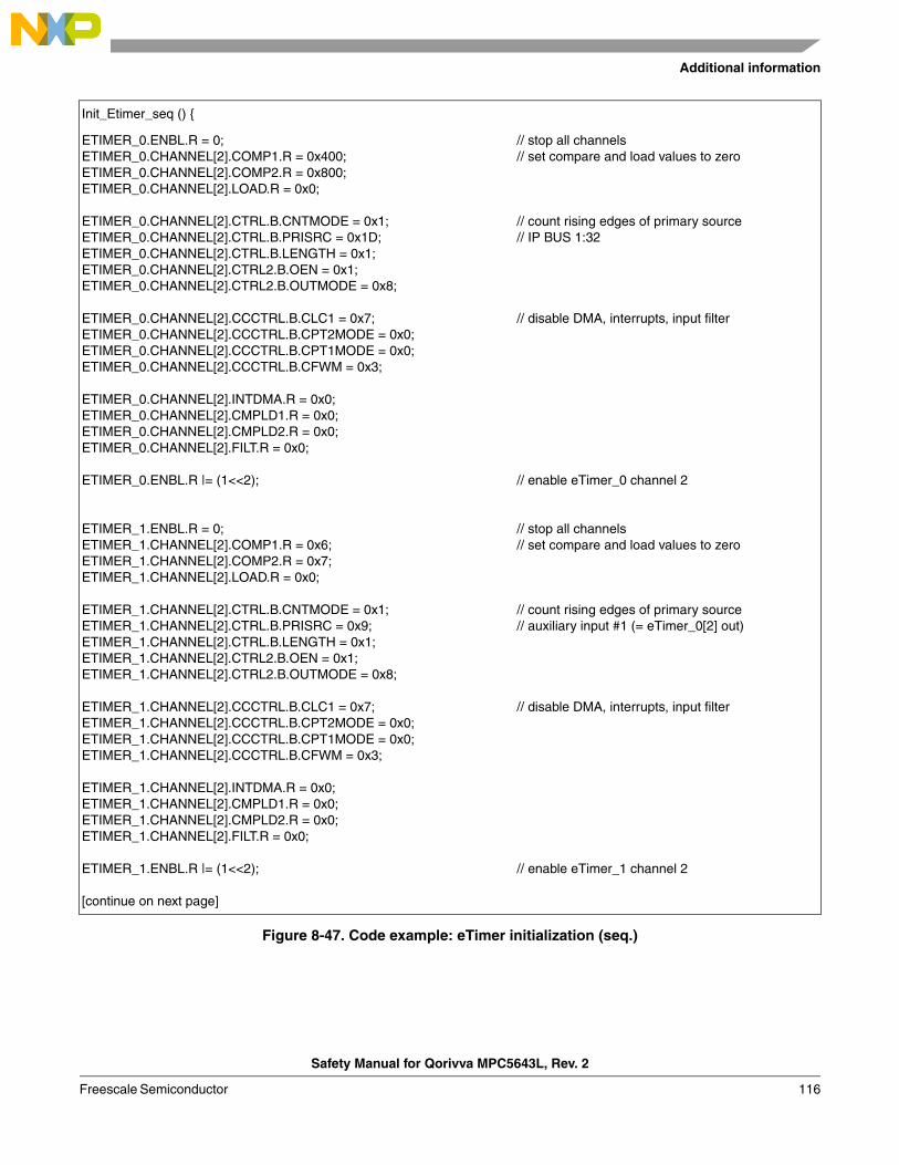
Additional information
Figure 8-47. Code example: eTimer initialization (seq.)
Init_Etimer_seq () {
ETIMER_0.ENBL.R = 0;ETIMER_0.CHANNEL[2].COMP1.R = 0x400;ETIMER_0.CHANNEL[2].COMP2.R = 0x800;ETIMER_0.CHANNEL[2].LOAD.R = 0x0;
ETIMER_0.CHANNEL[2].CTRL.B.CNTMODE = 0x1; ETIMER_0.CHANNEL[2].CTRL.B.PRISRC = 0x1D; ETIMER_0.CHANNEL[2].CTRL.B.LENGTH = 0x1;ETIMER_0.CHANNEL[2].CTRL2.B.OEN = 0x1;ETIMER_0.CHANNEL[2].CTRL2.B.OUTMODE = 0x8;
ETIMER_0.CHANNEL[2].CCCTRL.B.CLC1 = 0x7;ETIMER_0.CHANNEL[2].CCCTRL.B.CPT2MODE = 0x0;ETIMER_0.CHANNEL[2].CCCTRL.B.CPT1MODE = 0x0;ETIMER_0.CHANNEL[2].CCCTRL.B.CFWM = 0x3;
ETIMER_0.CHANNEL[2].INTDMA.R = 0x0;ETIMER_0.CHANNEL[2].CMPLD1.R = 0x0;ETIMER_0.CHANNEL[2].CMPLD2.R = 0x0;ETIMER_0.CHANNEL[2].FILT.R = 0x0;
ETIMER_0.ENBL.R |= (1<<2);
ETIMER_1.ENBL.R = 0;ETIMER_1.CHANNEL[2].COMP1.R = 0x6;ETIMER_1.CHANNEL[2].COMP2.R = 0x7;ETIMER_1.CHANNEL[2].LOAD.R = 0x0;
ETIMER_1.CHANNEL[2].CTRL.B.CNTMODE = 0x1; ETIMER_1.CHANNEL[2].CTRL.B.PRISRC = 0x9; ETIMER_1.CHANNEL[2].CTRL.B.LENGTH = 0x1;ETIMER_1.CHANNEL[2].CTRL2.B.OEN = 0x1;ETIMER_1.CHANNEL[2].CTRL2.B.OUTMODE = 0x8;
ETIMER_1.CHANNEL[2].CCCTRL.B.CLC1 = 0x7;ETIMER_1.CHANNEL[2].CCCTRL.B.CPT2MODE = 0x0;ETIMER_1.CHANNEL[2].CCCTRL.B.CPT1MODE = 0x0;ETIMER_1.CHANNEL[2].CCCTRL.B.CFWM = 0x3;
ETIMER_1.CHANNEL[2].INTDMA.R = 0x0;ETIMER_1.CHANNEL[2].CMPLD1.R = 0x0;ETIMER_1.CHANNEL[2].CMPLD2.R = 0x0;ETIMER_1.CHANNEL[2].FILT.R = 0x0;
ETIMER_1.ENBL.R |= (1<<2);
[continue on next page]
// stop all channels// set compare and load values to zero
// count rising edges of primary source// IP BUS 1:32
// disable DMA, interrupts, input filter
// enable eTimer_0 channel 2
// stop all channels// set compare and load values to zero
// count rising edges of primary source// auxiliary input #1 (= eTimer_0[2] out)
// disable DMA, interrupts, input filter
// enable eTimer_1 channel 2
Safety Manual for Qorivva MPC5643L, Rev. 2
Freescale Semiconductor 116
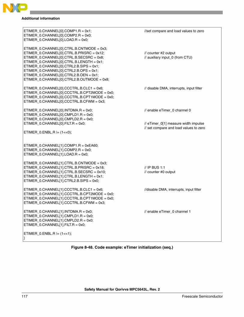
Additional information
Figure 8-48. Code example: eTimer initialization (seq.)
ETIMER_0.CHANNEL[0].COMP1.R = 0x1;ETIMER_0.CHANNEL[0].COMP2.R = 0x0;ETIMER_0.CHANNEL[0].LOAD.R = 0x0;
ETIMER_0.CHANNEL[0].CTRL.B.CNTMODE = 0x3; ETIMER_0.CHANNEL[0].CTRL.B.PRISRC = 0x12; ETIMER_0.CHANNEL[0].CTRL.B.SECSRC = 0x8;ETIMER_0.CHANNEL[0].CTRL.B.LENGTH = 0x1;ETIMER_0.CHANNEL[0].CTRL2.B.SIPS = 0x1;ETIMER_0.CHANNEL[0].CTRL2.B.OPS = 0x1;ETIMER_0.CHANNEL[0].CTRL2.B.OEN = 0x1;ETIMER_0.CHANNEL[0].CTRL2.B.OUTMODE = 0x8;
ETIMER_0.CHANNEL[0].CCCTRL.B.CLC1 = 0x6; ETIMER_0.CHANNEL[0].CCCTRL.B.CPT2MODE = 0x0;ETIMER_0.CHANNEL[0].CCCTRL.B.CPT1MODE = 0x0; ETIMER_0.CHANNEL[0].CCCTRL.B.CFWM = 0x3;
ETIMER_0.CHANNEL[0].INTDMA.R = 0x0;ETIMER_0.CHANNEL[0].CMPLD1.R = 0x0;ETIMER_0.CHANNEL[0].CMPLD2.R = 0x0;ETIMER_0.CHANNEL[0].FILT.R = 0x0;
ETIMER_0.ENBL.R |= (1<<0);
ETIMER_0.CHANNEL[1].COMP1.R = 0xEA60;ETIMER_0.CHANNEL[1].COMP2.R = 0x0;ETIMER_0.CHANNEL[1].LOAD.R = 0x0;
ETIMER_0.CHANNEL[1].CTRL.B.CNTMODE = 0x3; ETIMER_0.CHANNEL[1].CTRL.B.PRISRC = 0x18; ETIMER_0.CHANNEL[1].CTRL.B.SECSRC = 0x10;ETIMER_0.CHANNEL[1].CTRL.B.LENGTH = 0x1;ETIMER_0.CHANNEL[1].CTRL2.B.SIPS = 0x0;
ETIMER_0.CHANNEL[1].CCCTRL.B.CLC1 = 0x6;ETIMER_0.CHANNEL[1].CCCTRL.B.CPT2MODE = 0x0;ETIMER_0.CHANNEL[1].CCCTRL.B.CPT1MODE = 0x0;ETIMER_0.CHANNEL[1].CCCTRL.B.CFWM = 0x3;
ETIMER_0.CHANNEL[1].INTDMA.R = 0x0; ETIMER_0.CHANNEL[1].CMPLD1.R = 0x0;ETIMER_0.CHANNEL[1].CMPLD2.R = 0x0;ETIMER_0.CHANNEL[1].FILT.R = 0x0;
ETIMER_0.ENBL.R |= (1<<1);}
//set compare and load values to zero
// counter #2 output// auxiliary input_0 (from CTU)
// disable DMA, interrupts, input filter
// enable eTimer_0 channel 0
// eTimer_0[1] measure width impulse// set compare and load values to zero
// IP BUS 1:1// counter #0 output
//disable DMA, interrupts, input filter
// enable eTimer_0 channel 1
Safety Manual for Qorivva MPC5643L, Rev. 2
Freescale Semiconductor117
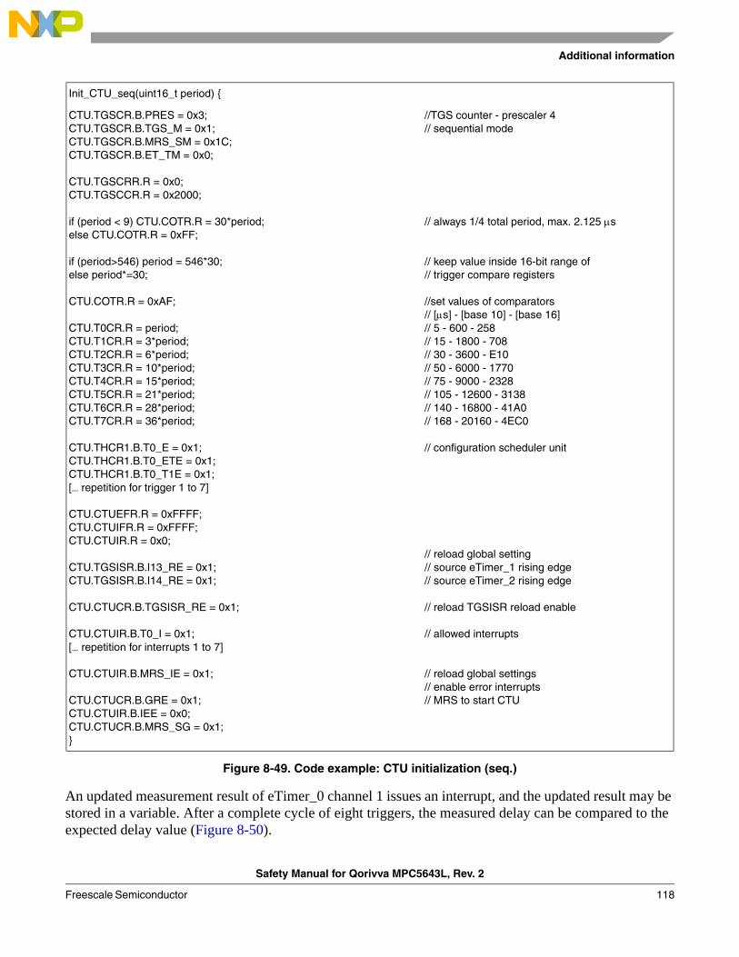
Additional information
Figure 8-49. Code example: CTU initialization (seq.)
An updated measurement result of eTimer_0 channel 1 issues an interrupt, and the updated result may be stored in a variable. After a complete cycle of eight triggers, the measured delay can be compared to the expected delay value (Figure 8-50).
Init_CTU_seq(uint16_t period) {
CTU.TGSCR.B.PRES = 0x3;CTU.TGSCR.B.TGS_M = 0x1;CTU.TGSCR.B.MRS_SM = 0x1C;CTU.TGSCR.B.ET_TM = 0x0;
CTU.TGSCRR.R = 0x0;CTU.TGSCCR.R = 0x2000;
if (period < 9) CTU.COTR.R = 30*period;else CTU.COTR.R = 0xFF;
if (period>546) period = 546*30;else period*=30;
CTU.COTR.R = 0xAF;
CTU.T0CR.R = period;CTU.T1CR.R = 3*period;CTU.T2CR.R = 6*period;CTU.T3CR.R = 10*period;CTU.T4CR.R = 15*period;CTU.T5CR.R = 21*period;CTU.T6CR.R = 28*period;CTU.T7CR.R = 36*period;
CTU.THCR1.B.T0_E = 0x1;CTU.THCR1.B.T0_ETE = 0x1;CTU.THCR1.B.T0_T1E = 0x1; [… repetition for trigger 1 to 7]
CTU.CTUEFR.R = 0xFFFF;CTU.CTUIFR.R = 0xFFFF;CTU.CTUIR.R = 0x0;
CTU.TGSISR.B.I13_RE = 0x1;CTU.TGSISR.B.I14_RE = 0x1;
CTU.CTUCR.B.TGSISR_RE = 0x1;
CTU.CTUIR.B.T0_I = 0x1;[… repetition for interrupts 1 to 7]
CTU.CTUIR.B.MRS_IE = 0x1;
CTU.CTUCR.B.GRE = 0x1;CTU.CTUIR.B.IEE = 0x0;CTU.CTUCR.B.MRS_SG = 0x1;}
//TGS counter - prescaler 4// sequential mode
// always 1/4 total period, max. 2.125 s
// keep value inside 16-bit range of// trigger compare registers
//set values of comparators// [s] - [base 10] - [base 16]// 5 - 600 - 258// 15 - 1800 - 708// 30 - 3600 - E10// 50 - 6000 - 1770// 75 - 9000 - 2328// 105 - 12600 - 3138// 140 - 16800 - 41A0// 168 - 20160 - 4EC0
// configuration scheduler unit
// reload global setting// source eTimer_1 rising edge// source eTimer_2 rising edge
// reload TGSISR reload enable
// allowed interrupts
// reload global settings// enable error interrupts// MRS to start CTU
Safety Manual for Qorivva MPC5643L, Rev. 2
Freescale Semiconductor 118
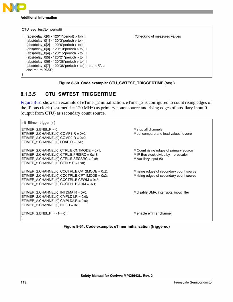
Additional information
Figure 8-50. Code example: CTU_SWTEST_TRIGGERTIME (seq.)
8.1.3.5 CTU_SWTEST_TRIGGERTIME
Figure 8-51 shows an example of eTimer_2 initialization. eTimer_2 is configured to count rising edges of the IP bus clock (assumed f = 120 MHz) as primary count source and rising edges of auxiliary input 0 (output from CTU) as secondary count source.
Figure 8-51. Code example: eTimer initialization (triggered)
CTU_seq_test(tol, period){
if ( (abs(delay_0[0] - 120*1*period) > tol) ||(abs(delay_0[1] - 120*3*period) > tol) ||(abs(delay_0[2] - 120*6*period) > tol) ||(abs(delay_0[3] - 120*10*period) > tol) ||(abs(delay_0[4] - 120*15*period) > tol) ||(abs(delay_0[5] - 120*21*period) > tol) ||(abs(delay_0[6] - 120*28*period) > tol) ||(abs(delay_0[7] - 120*36*period) > tol) ) return FAIL;else return PASS;
}
//checking of measured values
Init_Etimer_trigger () {
ETIMER_2.ENBL.R = 0;ETIMER_2.CHANNEL[0].COMP1.R = 0x0;ETIMER_2.CHANNEL[0].COMP2.R = 0x0;ETIMER_2.CHANNEL[0].LOAD.R = 0x0;
ETIMER_2.CHANNEL[0].CTRL.B.CNTMODE = 0x1;ETIMER_2.CHANNEL[0].CTRL.B.PRISRC = 0x18; ETIMER_2.CHANNEL[0].CTRL.B.SECSRC = 0x8; ETIMER_2.CHANNEL[0].CTRL2.R = 0x0;
ETIMER_2.CHANNEL[0].CCCTRL.B.CPT2MODE = 0x2;ETIMER_2.CHANNEL[0].CCCTRL.B.CPT1MODE = 0x2;ETIMER_2.CHANNEL[0].CCCTRL.B.CFWM = 0x3;ETIMER_2.CHANNEL[0].CCCTRL.B.ARM = 0x1;
ETIMER_2.CHANNEL[0].INTDMA.R = 0x0;ETIMER_2.CHANNEL[0].CMPLD1.R = 0x0;ETIMER_2.CHANNEL[0].CMPLD2.R = 0x0;ETIMER_2.CHANNEL[0].FILT.R = 0x0;
ETIMER_2.ENBL.R |= (1<<0);}
// stop all channels// set compare and load values to zero
// Count rising edges of primary source// IP Bus clock divide by 1 prescaler// Auxiliary input #0
// rising edges of secondary count source// rising edges of secondary count source
// disable DMA, interrupts, input filter
// enable eTimer channel
Safety Manual for Qorivva MPC5643L, Rev. 2
Freescale Semiconductor119

Additional information
Figure 8-52 shows an example of CTU initialization.
Figure 8-52. Code example: CTU initialization (triggered)
Figure 8-53 shows the consecutive CTU trigger event generation. The time of each rising edge is stored in CAPT_1 and CAPT_2 FIFOs. Once a capture occurs on capture circuit 1, capture circuit 1 is disarmed and capture circuit 2 is armed and vice versa. The safety integrity measure CTU_SWTEST_TRIGGERTIME (see Figure 8-54) calculates the period of the CTU signal and reports FAIL, in case the period does not match the expectations.
Figure 8-53. Timing of CAPT1 and CAPT2 values
Init_CTU_trigger(period) {
CTU.TGSCR.B.PRES = 0x3;CTU.TGSCR.B.TGS_M = 0x0;CTU.TGSCRR.R = 0x0;CTU.TGSCCR.R = 0xA8C;
if (period < 9) CTU.COTR.R = 120*period/4;else CTU.COTR.R = 0xFF;
CTU.CTUCR.B.T0_SG = 0x0;
if (period>546) period = 546 * 30;else period*=30;
CTU.T0CR.R = period;CTU.T1CR.R = 2*period;CTU.T2CR.R = 3*period;CTU.T3CR.R = 4*period;
CTU.THCR1.B.T0_E = 0x1;CTU.THCR1.B.T0_ETE = 0x1;CTU.THCR1.B.T0_T3E = 0x1;
[… repetition for timer 1 to 3]
CTU.CTUCR.B.GRE = 0x1;CTU.CTUIR.B.IEE = 1;}
// TGS counter - prescaler 4// triggered mode// 2700
// always 1/4 total period, max. 2.125 s
// keep value inside 16-bit range of // trigger compare registers
// set values of comparators
// configuration scheduler unit
// reload global setting// enable error interrupts
period period period
capt1_FIFO[0]temp[0]
capt2_FIFO[0]temp[2]
capt1_FIFO[1]temp[1]
capt2_FIFO[1]temp[3]
Safety Manual for Qorivva MPC5643L, Rev. 2
Freescale Semiconductor 120

Additional information
Figure 8-54. Code example: CTU_SWTEST_TRIGGERTIME (trig.)
8.1.3.6 CTU_HWSWTEST_TRIGGERNUM
Figure 8-55. Code example: CTU_HWSWTEST_TRIGGERNUM
CTU_SWTEST_TRIGGERTIME (period)
{temp[4] = {0,0,0,0};CTU.CTUCR.B.MRS_SG = 0x1;
while(ETIMER_2.CHANNEL[0].CTRL3.B.C2FCNT<2);
ETIMER_2.CHANNEL[0].CCCTRL.B.ARM = 0x0;
temp[0] = ETIMER_2.CHANNEL[0].CAPT1.R;temp[1] = ETIMER_2.CHANNEL[0].CAPT1.R;temp[2] = ETIMER_2.CHANNEL[0].CAPT2.R;temp[3] = ETIMER_2.CHANNEL[0].CAPT2.R;
ETIMER_2.CHANNEL[0].CCCTRL.B.ARM = 0x1;if (
((temp[2]-temp[0])!=120*period) ||((temp[3]-temp[1])!=120*period) ||((temp[1]-temp[2])!=120*period))
return FAIL;else return PASS; }
// MRS to start CTU (here just for // illustration)
// wait until two entries in FIFO 2
// stop counting to read values
// reading capture values from FIFO
// assuming fclock = 120 MHz
Parameters:period: expected time between two triggers. The value is in s
Return Values:PASS when difference fits into the toleranceFAIL otherwise
CTU_HWSWTEST_TRIGGERNUM_ISR() {
g_ctuefr = CTU.CTUEFR.R;CTU.CTUEFR.R = 0xFFFF;
if (g_ctuefr&(1<<11)); [place reaction here]if (g_ctuefr&(1<<9)); [place reaction here]if (g_ctuefr&(1<<8)); [place reaction here]if (g_ctuefr&(1<<7)); [place reaction here]if (g_ctuefr&(1<<6)); [place reaction here]if (g_ctuefr&(1<<5)); [place reaction here]if (g_ctuefr&(1<<4)); [place reaction here]if (g_ctuefr&(1<<3)); [place reaction here]if (g_ctuefr&(1<<1)); [place reaction here]}
// a critical event occurs it immediately attends// store the error cause in a variable
// external trigger generation overrun error// timer 4 trigger generation overrun error// timer 3 trigger generation overrun error// timer 2 trigger generation overrun error// timer 1 trigger generation overrun error// ADC command generation overrun error// TGS overrun error in sequential mode// Master Reload Signal overrun error// trigger overrun error (more than 8 EV) in TGS sequential mode
Safety Manual for Qorivva MPC5643L, Rev. 2
Freescale Semiconductor121

Additional information
8.1.3.7 CTU_HW_CFGINTEGRITY
Figure 8-56. Code example: CTU_HW_CFGINTEGRITY
8.1.4 Digital inputs
8.1.4.1 ETIMERI_SWTEST_CMP
This test is to redundantly read two PWM inputs. The pulse widths of the input signals are captured and compared for this test. However, other parameters of the input signal could be used if configured with a simple configuration change.
To demonstrate, this example uses hardcoded I/O and eTimer channels.
CTU_HW_CFGINTEGRITY (* store_var){
if ((*store_var & 0x1) || (*store_var & 0x8)) {return (FAIL);}
return (PASS);}
// if there was a reload error (MRS_RE) // (0x1) or an overrun (MRS_O) (0x8) the // configuration is/could be incorrect
Parameters*store_var: When the CTUEFR register is read, it's content is cleared. The original content is stored in address give by store_var
Return Values:PASS: no configuration errorFAIL: otherwise
Safety Manual for Qorivva MPC5643L, Rev. 2
Freescale Semiconductor 122

Additional information
Figure 8-57. Code example: ETIMERI_SWTEST_CMP
ETIMERI_SWTEST_CMP () {
SIUL.PCR[0].R = 0x0500; SIUL.PCR[4].R = 0x0500;
ETIMER_0.CHANNEL[0].CTRL1.R = 0x3800;ETIMER_0.CHANNEL[0].CCCTRL.R = 0x0065;
ETIMER_1.CHANNEL[0].CTRL1.R = 0x3800;ETIMER_1.CHANNEL[0].CCCTRL.R = 0x0065;
while(ETIMER_0.CHANNEL[0].STS.B.ICF1 == 0);eT0_time1 = ETIMER_0.CHANNEL[0].CAPT1.R;
while(ETIMER_1.CHANNEL[0].STS.B.ICF1 == 0);eT1_time1 = ETIMER_1.CHANNEL[0].CAPT1.R;
while(ETIMER_0.CHANNEL[0].STS.B.ICF2 == 0);eT0_time2 = ETIMER_0.CHANNEL[0].CAPT2.R;
while(ETIMER_1.CHANNEL[0].STS.B.ICF2 == 0);eT1_time2 = ETIMER_1.CHANNEL[0].CAPT2.R; eT0_Result = eT0_time2 - eT0_time1;eT1_Result = eT1_time2 - eT1_time1;
if ( (eT0_Result == eT1_Result)||(eT0_Result+1 == eT1_Result)|| (eT0_Result-1 == eT1_Result)) return eT1_Result;
else return error; }
// configure SIUL inputs// A[0] to eTimer_0 // A[4] to eTimer_1
// eTimer_0: configure period measurement// ARM, capture 1: rising, capture 2: falling
// eTimer_1: configure period measurement// ARM, capture 1: rising, capture 2: falling
// eTimer_0: wait for 1st edge to capture// eTimer_0: read time 1st edge captured at
// eTimer_1: wait for 1st edge to capture// eTimer_1: read time 1st edge captured at
// eTimer_0: wait for 2nd edge to capture// eTimer_0: read time 2nd edge captured at
// eTimer_1: wait for 2nd edge to capture// eTimer_1: read time 2nd edge captured at
// eTimer_0: calculate Period// eTimer_1: calculate Period
// Check if results are the same within one count
Parameters: none
Return values:error: Inputs did not matchvalue: Pulse widths matched and the value of the matching pulse width is returned.
Safety Manual for Qorivva MPC5643L, Rev. 2
Freescale Semiconductor123

Additional information
8.1.4.2 GPI_SWTEST_CMP
This test is to redundantly read two digital inputs. If both read values are identical, the read value is given as output.
Figure 8-58. Code example: GPI_SWTEST_CMP
8.1.5 Digital outputs
8.1.5.1 GPODW_SWAPP_WRITE
This function is to redundantly output two digital values. One Parallel GPIO Pad Data Out register is used to have both output signals change their value at the same time. Readback of written register is required.
GPI_SWTEST_CMP (pin1, pin2){
if(pin1== pin2) return read_error;
SIUL.PCR[pin1].R = 0x0100;SIUL.PCR[pin2].R = 0x0100;
pin1_val = SIUL.GPDI[pin1].R;pin2_val = SIUL.GPDI[pin2].R;
if(pin1_val != pin2_val) return read_error;else return pin1_val;}
// Make sure that I/Os are different
// Configure SIUL GPIO as input
// Read Inputs
// Check values match and return
Parameterspin1: Defines the first of the two input GPIO to be read pin2: Defines the second GPIO to be read
Return values0: Input value read as low on both pin 1 and pin21: Input value read as high on both pin1 and pin2read_error: Input values read on pin1 and pin2 do not match
Safety Manual for Qorivva MPC5643L, Rev. 2
Freescale Semiconductor 124
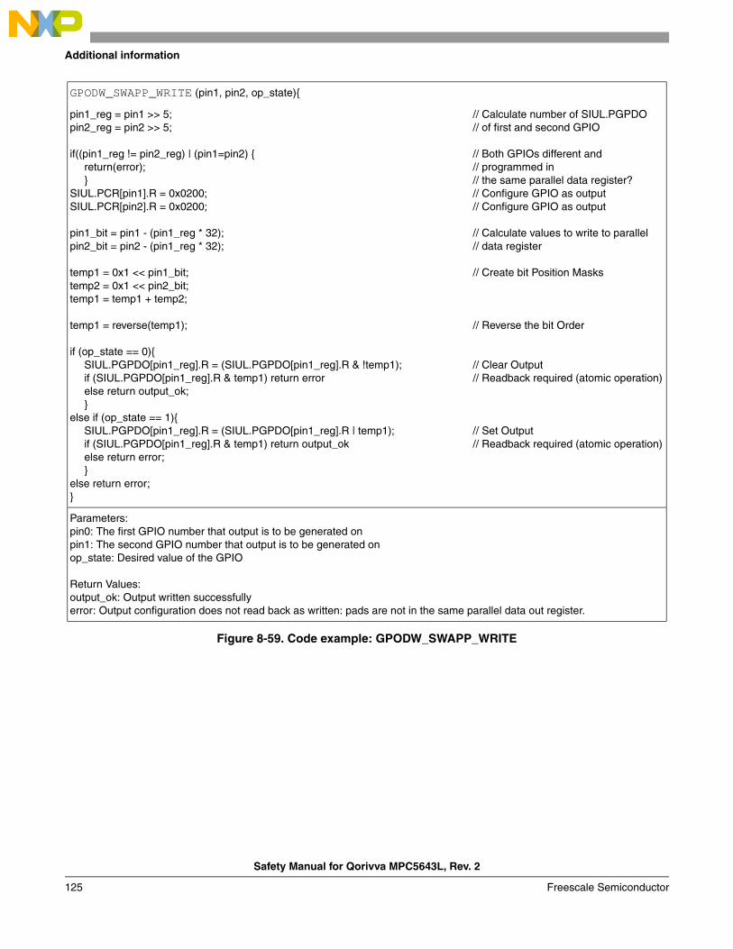
Additional information
Figure 8-59. Code example: GPODW_SWAPP_WRITE
GPODW_SWAPP_WRITE (pin1, pin2, op_state){
pin1_reg = pin1 >> 5;pin2_reg = pin2 >> 5;
if((pin1_reg != pin2_reg) | (pin1=pin2) {return(error);}
SIUL.PCR[pin1].R = 0x0200; SIUL.PCR[pin2].R = 0x0200;
pin1_bit = pin1 - (pin1_reg * 32);pin2_bit = pin2 - (pin1_reg * 32);
temp1 = 0x1 << pin1_bit;temp2 = 0x1 << pin2_bit; temp1 = temp1 + temp2;
temp1 = reverse(temp1);
if (op_state == 0){SIUL.PGPDO[pin1_reg].R = (SIUL.PGPDO[pin1_reg].R & !temp1);if (SIUL.PGPDO[pin1_reg].R & temp1) return errorelse return output_ok;}
else if (op_state == 1){SIUL.PGPDO[pin1_reg].R = (SIUL.PGPDO[pin1_reg].R | temp1);if (SIUL.PGPDO[pin1_reg].R & temp1) return output_okelse return error;}
else return error;}
// Calculate number of SIUL.PGPDO// of first and second GPIO
// Both GPIOs different and// programmed in // the same parallel data register?// Configure GPIO as output// Configure GPIO as output
// Calculate values to write to parallel// data register
// Create bit Position Masks
// Reverse the bit Order
// Clear Output// Readback required (atomic operation)
// Set Output// Readback required (atomic operation)
Parameters:pin0: The first GPIO number that output is to be generated onpin1: The second GPIO number that output is to be generated onop_state: Desired value of the GPIO
Return Values:output_ok: Output written successfullyerror: Output configuration does not read back as written: pads are not in the same parallel data out register.
Safety Manual for Qorivva MPC5643L, Rev. 2
Freescale Semiconductor125

Additional information
8.1.5.2 GPOIRB_SWTEST_CMP
This software test executes the comparison between the desired output values and the value read back via internal read back configuration.
Figure 8-60. Code example: GPOIRB_SWTEST_CMP
8.1.5.3 GPOERB_SWTEST_CMP
The output is externally connected to an input pin. After writing the output value to the pin, the input is read to check that the correct output value is present.
Figure 8-61. Code example: GPOERB_SWTEST_CMP
GPOIRB_SWTEST_CMP (pin, op_state){
SIUL.PCR[pin].R= 0x0300;
SIUL.GPDO[pin].R = op_state;
if(SIU.GPDI[pin].R != op_state) return(error);else return(output_ok); }
// Configure Pin[pin] as GPIO output with enabled input buffer
// Set Pin[pin] Output State
// Does read back value matches the desired op_state?
Parameters:pin: The GPIO number that output is to be generated on and read back from.op_state: Desired value of the GPIO
Return values:output_ok: Input value read back matches written outputinput_error: Output does not read back as written
GPOERB_SWTEST_CMP (pin_op, pin_rb, op_state) {
SIUL.PCR[pin_op].R= 0x0200; SIUL.PCR[pin_rb].R= 0x0100;
SIUL.GPDO[pin_op].R = op_state;
[short pause]
if(SIU.GPDI[pin_rb].R != op_state) return(error);else return(output_ok); }
// Configure Pin[pin_op] as GPIO output// Configure Pin[pin_rb] as GPIO input
// Set Pin[pin_op] Output State
// There is a short propagation delay before the output is // present at the input of the read back pin.
// Does read back value match the desired out_val?
Parameters:pin_op: The GPIO number that output is to be generated on.pin_rb: The GPIO number that the output is to be read back on.op_state: Desired value of the GPIO
Return values:output_ok: Input value read back matches output writtenerror: Output does not read back as written
Safety Manual for Qorivva MPC5643L, Rev. 2
Freescale Semiconductor 126

Additional information
8.1.5.4 PWMRB_SWTEST_CMP
For this example, FlexPWM_0 is used to generate a PWM output and eTimer_1 is used to read back and verify the output.
In this test case, the pulse width is measured and used for comparison. The eTimer could be configured to compare the period by changing the configuration to capture the times at which 2 consecutive edges of the same type occur.
The result might be a few counts different from the output signal. It is good practice to take this into account on the system level.
The FlexPWM is configured to generate a center aligned PWM. This configuration is shown in Figure 8-62.
Figure 8-62. PWM output signal and timing
Application software validates the values read by comparing these with expected values (340 (154h) in this example).
Safety Manual for Qorivva MPC5643L, Rev. 2
Freescale Semiconductor127
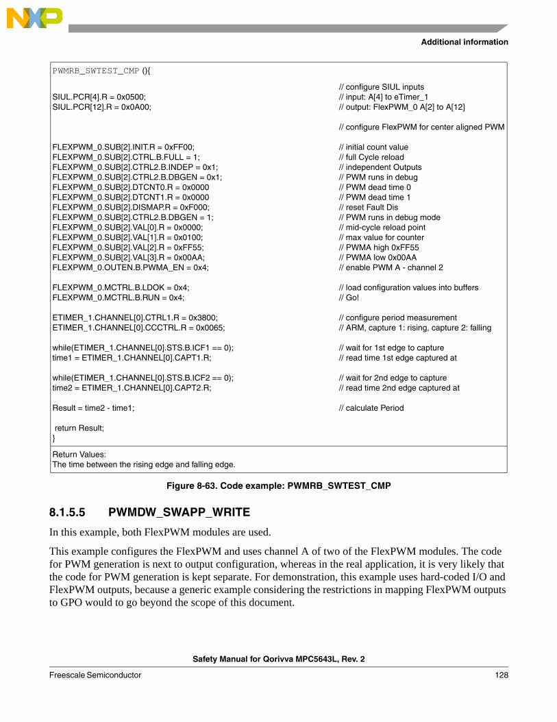
Additional information
Figure 8-63. Code example: PWMRB_SWTEST_CMP
8.1.5.5 PWMDW_SWAPP_WRITE
In this example, both FlexPWM modules are used.
This example configures the FlexPWM and uses channel A of two of the FlexPWM modules. The code for PWM generation is next to output configuration, whereas in the real application, it is very likely that the code for PWM generation is kept separate. For demonstration, this example uses hard-coded I/O and FlexPWM outputs, because a generic example considering the restrictions in mapping FlexPWM outputs to GPO would to go beyond the scope of this document.
PWMRB_SWTEST_CMP (){
SIUL.PCR[4].R = 0x0500; SIUL.PCR[12].R = 0x0A00;
FLEXPWM_0.SUB[2].INIT.R = 0xFF00;FLEXPWM_0.SUB[2].CTRL.B.FULL = 1;FLEXPWM_0.SUB[2].CTRL2.B.INDEP = 0x1;FLEXPWM_0.SUB[2].CTRL2.B.DBGEN = 0x1;FLEXPWM_0.SUB[2].DTCNT0.R = 0x0000FLEXPWM_0.SUB[2].DTCNT1.R = 0x0000FLEXPWM_0.SUB[2].DISMAP.R = 0xF000; FLEXPWM_0.SUB[2].CTRL2.B.DBGEN = 1;FLEXPWM_0.SUB[2].VAL[0].R = 0x0000;FLEXPWM_0.SUB[2].VAL[1].R = 0x0100;FLEXPWM_0.SUB[2].VAL[2].R = 0xFF55;FLEXPWM_0.SUB[2].VAL[3].R = 0x00AA;FLEXPWM_0.OUTEN.B.PWMA_EN = 0x4;
FLEXPWM_0.MCTRL.B.LDOK = 0x4;FLEXPWM_0.MCTRL.B.RUN = 0x4;
ETIMER_1.CHANNEL[0].CTRL1.R = 0x3800;ETIMER_1.CHANNEL[0].CCCTRL.R = 0x0065;
while(ETIMER_1.CHANNEL[0].STS.B.ICF1 == 0);time1 = ETIMER_1.CHANNEL[0].CAPT1.R;
while(ETIMER_1.CHANNEL[0].STS.B.ICF2 == 0);time2 = ETIMER_1.CHANNEL[0].CAPT2.R;
Result = time2 - time1;
return Result; }
// configure SIUL inputs// input: A[4] to eTimer_1// output: FlexPWM_0 A[2] to A[12]
// configure FlexPWM for center aligned PWM
// initial count value// full Cycle reload// independent Outputs// PWM runs in debug// PWM dead time 0// PWM dead time 1// reset Fault Dis// PWM runs in debug mode// mid-cycle reload point// max value for counter// PWMA high 0xFF55// PWMA low 0x00AA// enable PWM A - channel 2
// load configuration values into buffers // Go!
// configure period measurement// ARM, capture 1: rising, capture 2: falling
// wait for 1st edge to capture// read time 1st edge captured at
// wait for 2nd edge to capture// read time 2nd edge captured at
// calculate Period
Return Values:The time between the rising edge and falling edge.
Safety Manual for Qorivva MPC5643L, Rev. 2
Freescale Semiconductor 128

Additional information
If the content of the PWM outputs are changed, care must be taken as the outputs can not be updated at the same time. Therefore for a short period of time both outputs could be different.
Figure 8-64. Code example: PWMDW_SWAPP_WRITE
PWMDW_SWAPP_WRITE (){
FLEXPWM_0.SUB[2].INIT.R = 0xFF00;FLEXPWM_0.SUB[2].CTRL.B.FULL = 1;FLEXPWM_0.SUB[2].CTRL2.B.INDEP = 0x1;FLEXPWM_0.SUB[2].CTRL2.B.DBGEN = 0x1;FLEXPWM_0.SUB[2].DTCNT0.R = 0x0000;FLEXPWM_0.SUB[2].DTCNT1.R = 0x0000;FLEXPWM_0.SUB[2].DISMAP.R = 0xF000;FLEXPWM_0.SUB[2].CTRL2.B.DBGEN = 1;FLEXPWM_0.SUB[2].VAL[0].R = 0x0000;FLEXPWM_0.SUB[2].VAL[1].R = 0x0100; FLEXPWM_0.SUB[2].VAL[2].R = 0xFF55;FLEXPWM_0.SUB[2].VAL[3].R = 0x00AA; FLEXPWM_0.SUB[2].VAL[4].R = 0xFFAA; FLEXPWM_0.SUB[2].VAL[5].R = 0x0055;
FLEXPWM_0.OUTEN.B.PWMA_EN = 0x4;
FLEXPWM_0.MCTRL.B.LDOK = 0x4;FLEXPWM_0.MCTRL.B.RUN = 0x4;
FLEXPWM_1.SUB[0].INIT.R = 0xFF00;FLEXPWM_1.SUB[0].CTRL.B.FULL = 1;FLEXPWM_1.SUB[0].CTRL2.B.INDEP = 0x1;FLEXPWM_1.SUB[0].CTRL2.B.DBGEN = 0x1; FLEXPWM_1.SUB[0].DTCNT0.R = 0x0000; FLEXPWM_1.SUB[0].DTCNT1.R = 0x0000; FLEXPWM_1.SUB[0].DISMAP.R = 0xF000; / FLEXPWM_1.SUB[0].CTRL2.B.DBGEN = 1; FLEXPWM_1.SUB[0].VAL[0].R = 0x0000; FLEXPWM_1.SUB[0].VAL[1].R = 0x0100; FLEXPWM_1.SUB[0].VAL[2].R = 0xFF55; FLEXPWM_1.SUB[0].VAL[3].R = 0x00AA; FLEXPWM_1.SUB[0].VAL[4].R = 0xFFAA; FLEXPWM_1.SUB[0].VAL[5].R = 0x0055;
FLEXPWM_1.OUTEN.B.PWMA_EN = 0x1;
FLEXPWM_1.MCTRL.B.LDOK = 0x1;FLEXPWM_1.MCTRL.B.RUN = 0x1;
SIUL.PCR[12].R = 0x0A00; SIUL.PCR[117].R = 0x0600;}
// Initial count value// Full Cycle reload// Independent Outputs// PWM runs in debug// PWMA dead time// PWMB dead time// Reset Fault Dis// PWM runs in debug mode// Mid-Cycle Reload Point// Max value for counter// Max value for counter// PWMA Low 0x00AA// PWMB High 0xFFAA// PWMB Low 0x0055
// Enable PWM A
// Load configuration values into buffers// Go!
// Initial count value// Full Cycle reload// Independent Outputs// PWM runs in debug// PWMA dead time// PWMB dead time// Reset Fault Dis// PWM runs in debug mode// Mid-Cycle Reload Point// Max value for counter// PWMA High 0xFF55// PWMA Low 0x00AA// PWMB High 0xFFAA// PWMB Low 0x0055
// Enable PWM A
// Load configuration values into buffers// Go!
// configure SIUL outputs// FlexPWM_0 A[2] to A[12]// FlexPWM_1 A[0] to H[5]
Safety Manual for Qorivva MPC5643L, Rev. 2
Freescale Semiconductor129

Additional information
8.1.6 Analog inputs
8.1.6.1 ADC_SWTEST_TEST1
Figure 8-65 and Figure 8-66 show an example for the ADC_SWTEST_TEST1. This test exploits the presampling feature of the ADC by using a reference voltage. Presampling allows to precharge or discharge the ADC internal capacitor before it starts the sampling and conversion phases of the analog input coming from pads.
Figure 8-65 shows the ADC_SWTEST_TEST1 configuration using ADC_0. Depending on the type of input signal to the ADC, VDD_HV_ADR, VSS_HV_ADR, or alternating between these, may be used for this function. This function may also be used for ADC_1.
Figure 8-65. Code example: ADC_SWTEST_TEST1
Figure 8-66 shows the execution of ADC_SWTEST_TEST1. This function is called when an end of chain interrupt occurs on ADC_0. This function tests whether the converted value is near to the value of a converted reference value. If the converted value is very near to the value of a converted reference voltage (for example, FFFh or 0), an open failure, or misconfiguration, of the multiplexing circuit is assumed. In this case, g_ADC0_SWTEST_TEST1_result = 1, which indicates a failed test. In this example, all channels are tested. If fewer channels are used in an application, the unused channels must be excluded from testing.
ADC0_SWTEST_TEST1_Init_ADC(){
ADC0.MCR.B.MODE = 0;ADC0.NCMR0.B.CH0 = 1;ADC0.NCMR0.B.CH1 = 1;[ all other used channels]
SIUL.PCR[23].R=0x2100;SIUL.PCR[24].R=0x2100;[ all other used channels]
ADC0.PSCR.B.PREVAL0=0;ADC0.PSCR.B.PREVAL1=0;ADC0.PSCR.B.PREVAL2=0;ADC0.PSCR.B.PRECONV=0;ADC0.PSR0.R=0xFFFF;
[VSS_HV_ADR0 can be used alternatively]
ADC0.IMR.B.MSKECH=1;}
// Set one shot mode// Enable channel 0// Enable channel 1
// ADC_0: enable B[7] for AN[0]// ADC_0: enable B[8] for AN[1]
// Select VDD_HV_ADR0 as presampling voltage// Select VDD_HV_ADR0 as presampling voltage (errata #4016)// Select VDD_HV_ADR0 as presampling voltage (errata #4016)// The ADC performs a sampling followed by a conversion // Presampling enabled for all used channels 0-15
// Application dependent
// Configuration of End of Chain interrupt
Safety Manual for Qorivva MPC5643L, Rev. 2
Freescale Semiconductor 130
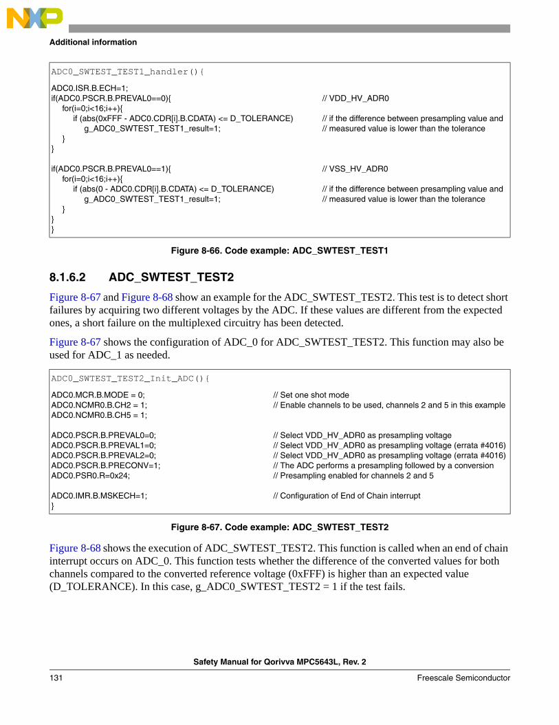
Additional information
Figure 8-66. Code example: ADC_SWTEST_TEST1
8.1.6.2 ADC_SWTEST_TEST2
Figure 8-67 and Figure 8-68 show an example for the ADC_SWTEST_TEST2. This test is to detect short failures by acquiring two different voltages by the ADC. If these values are different from the expected ones, a short failure on the multiplexed circuitry has been detected.
Figure 8-67 shows the configuration of ADC_0 for ADC_SWTEST_TEST2. This function may also be used for ADC_1 as needed.
Figure 8-67. Code example: ADC_SWTEST_TEST2
Figure 8-68 shows the execution of ADC_SWTEST_TEST2. This function is called when an end of chain interrupt occurs on ADC_0. This function tests whether the difference of the converted values for both channels compared to the converted reference voltage (0xFFF) is higher than an expected value (D_TOLERANCE). In this case, g_ADC0_SWTEST_TEST2 = 1 if the test fails.
ADC0_SWTEST_TEST1_handler(){
ADC0.ISR.B.ECH=1;if(ADC0.PSCR.B.PREVAL0==0){
for(i=0;i<16;i++){if (abs(0xFFF - ADC0.CDR[i].B.CDATA) <= D_TOLERANCE)
g_ADC0_SWTEST_TEST1_result=1;}
}
if(ADC0.PSCR.B.PREVAL0==1){for(i=0;i<16;i++){
if (abs(0 - ADC0.CDR[i].B.CDATA) <= D_TOLERANCE)g_ADC0_SWTEST_TEST1_result=1;
}}}
// VDD_HV_ADR0
// if the difference between presampling value and// measured value is lower than the tolerance
// VSS_HV_ADR0
// if the difference between presampling value and // measured value is lower than the tolerance
ADC0_SWTEST_TEST2_Init_ADC(){
ADC0.MCR.B.MODE = 0;ADC0.NCMR0.B.CH2 = 1;ADC0.NCMR0.B.CH5 = 1;
ADC0.PSCR.B.PREVAL0=0;ADC0.PSCR.B.PREVAL1=0;ADC0.PSCR.B.PREVAL2=0;ADC0.PSCR.B.PRECONV=1;ADC0.PSR0.R=0x24;
ADC0.IMR.B.MSKECH=1;}
// Set one shot mode// Enable channels to be used, channels 2 and 5 in this example
// Select VDD_HV_ADR0 as presampling voltage// Select VDD_HV_ADR0 as presampling voltage (errata #4016)// Select VDD_HV_ADR0 as presampling voltage (errata #4016)// The ADC performs a presampling followed by a conversion // Presampling enabled for channels 2 and 5
// Configuration of End of Chain interrupt
Safety Manual for Qorivva MPC5643L, Rev. 2
Freescale Semiconductor131

Additional information
Figure 8-68. Code example: ADC_SWTEST_TEST2
In this example, channel 2 and 5 are used. Depending on the application, a pair of other channels can be chosen as well.
8.1.6.3 ADC_SWTEST_CMP
Figure 8-69. Code example: ADC_SWTEST_CMP
ADC0_SWTEST_TEST2_handler(){
ADC0.ISR.B.ECH=1;if(ADC0.PSCR.B.PREVAL0==0) {
g_ADC0_channel2=ADC0.CDR[2].B.CDATA;ADC0.PSCR.B.PREVAL0=1;ADC0.PSCR.B.PREVAL1=1;ADC0.PSCR.B.PREVAL2=1;ADC0.MCR.B.NSTART=1;
}if(ADC0.PSCR.B.PREVAL0==1){
if (abs(0xFFF - g_ADC0_channel2 + ADC0.CDR[5].B.CDATA) >= D_TOLERANCE) g_ADC0_SWTEST_TEST2_result=1;
ADC0.PSCR.B.PREVAL0=0;ADC0.PSCR.B.PREVAL1=0;ADC0.PSCR.B.PREVAL2=0;
}
// VDD_HV_ADR0// Store channel 2 result for high reference// Select VSS_HV_ADR0 as presampling voltage// Select VSS_HV_ADR0 as presampling voltage// Select VSS_HV_ADR0 as presampling voltage// Start the chain conversion.
// VSS_HV_ADR0
// Select VDD_HV_ADR0 as presampling voltage// Select VDD_HV_ADR0 as presampling voltage// Select VDD_HV_ADR0 as presampling voltage
ADC_SWTEST_CMP (tol, ADCH1, ADCH2){
ADC0.MCR.B.NSTART = 1;ADC1.MCR.B.NSTART = 1;
while ((!ADC0.CDR[ADCH1].B.VALID) || (!ADC1.CDR[ADCH2].B.VALID))
{;}
if (abs(ADC0.CDR[ADCH1].B.CDATA - ADC1.CDR[ADCH2].B.CDATA) >= tol) return (FAIL);return (PASS);
}
// start a single conversion with ADC_0// start a single conversion with ADC_1
// wait till conversion is complete
// difference between the results is // greater than the tolerance
Parameters:tol: Defines the allowed difference from the referenceADCH1: first ADC channelADCH2: second ADC channel
Return Values:PASS: results match within the given toleranceFAIL: results do not match
Safety Manual for Qorivva MPC5643L, Rev. 2
Freescale Semiconductor 132

Additional information
8.2 Checks and configurationsBelow is a list of the minimum number of checks by the safety integrity functions which need to pass before executing any safety function:
• Lockstep mode check
• STCU check
• Flash Array Integrity Self check
• SUPPLY SELF-TEST
• Temperature Sensor check
• SWT enabled
• CMU check
• PLL_SW_CHECK
• IRC_SW_CHECK
• PMU check
• FCCU_F[n] signal check1
Correct execution of these checks is a prerequisite for functional safety.
Below lists all checks that are repeated (at least once every FTTI) during normal operation of the device:
• FLASH_SW_ECCTEST
• Temperature check
• CRC calculation
1. Requirement for single FCCU pin usage only.
Safety Manual for Qorivva MPC5643L, Rev. 2
Freescale Semiconductor133

Further information
9 Further information
9.1 Acronyms and abbreviationsA short list of acronyms and abbreviations used in this document is summarized for completeness:
Table 9-1. Acronyms and abbreviations
Terms Meanings
ADC Analog-to-Digital Converter
BAM Boot Assist Module
BIST Built-in Self-Test
BIU Bus Interface Unit
CF Critical Fault
CCF Common Cause Failure
CMF Common Mode Failure
CMU Clock Monitor Unit
CRC Cyclic Redundancy Check
CTU Cross-Triggering Unit
DC Diagnostic Coverage
DMA Direct Memory Access
DED Dual Error Detection
ECC Error Correcting Code
ECSM Error Correction Status Module
ECU Electronic Control Unit
eDMA Enhanced Direct Memory Access
ERRM Error Out Monitor function
EXWD External Timeout (Watchdog) function
FCCU Fault Collection and Control Unit
FMEDA Failure Modes, Effects, and Diagnostic Analysis
FMPLL Frequency-Modulated Phase-Locked Loop
FTTI Single-Point Fault Tolerant Time Interval
GPIO General Purpose I/O
HVD High Voltage Detector
INTC Interrupt Controller
LBIST Logic Built-In Self-Test
L-FTTI Latent Fault Tolerant Time Interval
Safety Manual for Qorivva MPC5643L, Rev. 2
Freescale Semiconductor 134

Further information
9.2 Safety Application Guide tag differencesTable 9-2 shows all tags that differ from the tags of the Safety Application Guide (Rev. 7).
All I/O-related mandatory requirements from the Safety Application Guide are not listed as a requirement in this safety manual, as the actual implementation is application specific and other solutions may be
LOC Loss-of-clock
LOL Loss-of-lock
LVD Low Voltage Detector
MBIST Memory Built-In Self-Test
MC_CGM Clock Generation Module
MC_ME Mode Entry
MC_RGM Reset Generation Module
MCU Microcontroller Unit
MPU Memory Protection Unit
NCF Noncritical Fault
NMI Nonmaskable Interrupt
NVM Nonvolatile Memory
PMU Power Management Unit
PSM Power Supply and Monitor function
PWM Pulse Width Modulation
RCCU Redundancy Control and Checking Unit
SAG Safety Application Guide
SEC Single Error Correction
SFF Safe Failure Fraction
SIL Safety Integrity Level
SM Safety Manual
SoR Sphere of Replication
SSCM System Status and Configuration Module
STCU Self-Test Control Unit
SWG Sine Wave Generator
SWT Software Watchdog Timer
XOSC External Oscillator
Table 9-1. Acronyms and abbreviations (continued)
Terms Meanings
Safety Manual for Qorivva MPC5643L, Rev. 2
Freescale Semiconductor135

Further information
appropriate. Redundant mandatory requirements, which are listed more than once in the Safety Application Guide are also not used in this document.
Table 9-2. Safety Application Guide tag differences
Tag Remark
Duplicate mandatory requirements only listed once
[SM_023] redundant to [\SM_019] [end]
[SM_026] redundant to [\SM_038] [end]
[SM_029] redundant to [\SM_019] [end]
[SM_042] redundant to [\SM_019] [end]
[SM_045] redundant to [\SM_019] [end]
[SM_053] redundant to [\SM_019] [end]
[SM_056] redundant to [\SM_051] [end]
[SM_081] redundant to [\SM_004] [end]
Mandatory requirements belonging to I/O are changed to recommendation or implementation hint
[SM_018] I/O function: Double Read Digital Inputs [end]
[SM_020] I/O function: Double Read PWM Inputs [end]
[SM_021] I/O function: Double Read PWM Inputs [end]
[SM_022] I/O function: Double Read PWM Inputs [end]
[SM_024] I/O function Double Read Encoder Inputs [end]
[SM_025] I/O function: Double Read Encoder Inputs [end]
[SM_027] I/O function Double Read Encoder Inputs [end]
[SM_028] I/O function: Double Read Encoder Inputs [end]
[SM_030] I/O function: Single Write Digital Outputs With Read Back [end]
[SM_031] I/O function: Single Write Digital Outputs With Read Back [end]
[SM_032] I/O function: Single Write Digital Outputs With Read Back [end]
[SM_033] I/O function: Double Write Digital Outputs [end]
[SM_034] I/O function: Double Write Digital Outputs [end]
[SM_035] I/O function: Double Write Digital Outputs [end]
[SM_036] I/O function: Double Write Digital Outputs [end]
[SM_037] I/O function: Double Write PWM Outputs [end]
[SM_039] I/O function: Double Write PWM Outputs [end]
[SM_040] I/O function: Double Write PWM Outputs [end]
[SM_041] I/O function: Double Write PWM Outputs [end]
[SM_043] I/O function: Single Write PWM Outputs With Read Back [end]
[SM_044] I/O function: Single Write PWM Outputs With Read Back [end]
Safety Manual for Qorivva MPC5643L, Rev. 2
Freescale Semiconductor 136

Further information
[SM_049] I/O function: Single Read Analog Inputs [end]
[SM_054] I/O function: Double Read Analog Inputs [end]
[SM_057] I/O function: Double Read Analog Inputs [end]
[SM_058] I/O function: Double Read Analog Inputs [end]
Others
[SM_013] sema4- changed to recommendation [end]
[SM_046] eTimer capture flag (eTimer_n_STS[ICFn]) [end]
[\SM_063] neither used in Safety Application Guide nor in Safety Manual
[SM_077] no requirement [end]
[SM_078] no requirement [end]
[SM_085] covered by newly phrased [\SM_084] [end]
New
[\SM_702] taking device errata into account
[\SM_703] system transitions to a safe state when MPC5643L is in reset state
[\SM_704] system transitions to a safe state when MPC5643L is completely unpowered
[\SM_708] ADC check
Table 9-2. Safety Application Guide tag differences (continued)
Tag Remark
Safety Manual for Qorivva MPC5643L, Rev. 2
Freescale Semiconductor137

Document revision history
10 Document revision historyTable 10-1 summarizes revisions to this document.
Table 10-1. Revision history
Revision Date Description of changes
1 02/2013 Initial release
2 04/2013 Updated revision number of previous revision history to 1.Added note on front page, “(NOTE: Replaces the Safety Application Guide for MPC5643L – MPC5643LSAG)”.
Safety Manual for Qorivva MPC5643L, Rev. 2
Freescale Semiconductor 138


![MPC5643L Dual Motor Controller Board User GuideR363 populated M1 PFC UNI-3 M1 PFC output signal is connected to GPIO G[7] (PWM0-B3). R364 populated M2 PFC. MPC5643L Dual Motor Controller](https://img.pdfslide.us/doc/110x75/603986c4cefa7440cf45045c/mpc5643l-dual-motor-controller-board-user-guide-r363-populated-m1-pfc-uni-3-m1-pfc.jpg)