Embed Size (px)
Citation preview
Safe‐Operating Areas (SOAs) forReliable High‐Voltage Analog Devices
J.W. McPherson , Ph.D.
IEEE FellowTexas Instruments Senior Fellow Emeritus
McPherson Reliability Consulting, LLC
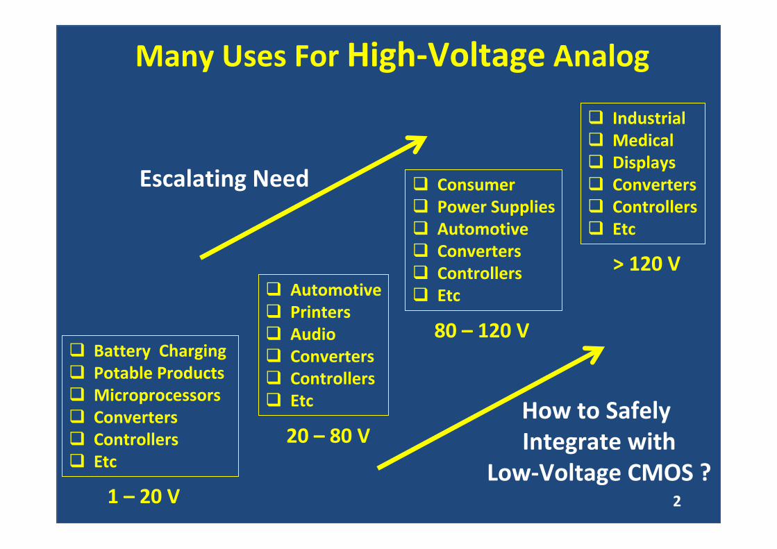
Many Uses For High‐Voltage Analog
Battery ChargingPotable ProductsMicroprocessors ConvertersControllersEtc
1 – 20 V
AutomotivePrintersAudioConvertersControllersEtc
ConsumerPower SuppliesAutomotiveConvertersControllers Etc
IndustrialMedical DisplaysConvertersControllersEtc
20 – 80 V
80 – 120 V
> 120 V
How to Safely Integrate with
Low‐Voltage CMOS ?
Escalating Need
2
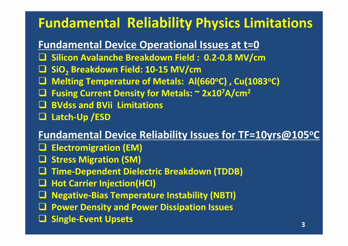
Fundamental Reliability Physics LimitationsFundamental Device Operational Issues at t=0
Silicon Avalanche Breakdown Field : 0.2‐0.8 MV/cmSiO2 Breakdown Field: 10‐15 MV/cm Melting Temperature of Metals: Al(660oC) , Cu(1083oC)Fusing Current Density for Metals: ~ 2x10⁷A/cm2
BVdss and BVii Limitations Latch‐Up /ESD
Fundamental Device Reliability Issues for TF=10yrs@105oCElectromigration (EM)Stress Migration (SM)Time‐Dependent Dielectric Breakdown (TDDB)Hot Carrier Injection(HCI)Negative‐Bias Temperature Instability (NBTI)Power Density and Power Dissipation IssuesSingle‐Event Upsets
3
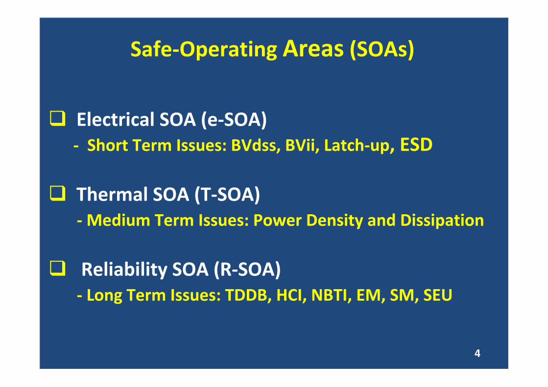
Safe‐Operating Areas (SOAs)
Electrical SOA (e‐SOA) ‐ Short Term Issues: BVdss, BVii, Latch‐up, ESD
Thermal SOA (T‐SOA)‐Medium Term Issues: Power Density and Dissipation
Reliability SOA (R‐SOA)‐ Long Term Issues: TDDB, HCI, NBTI, EM, SM, SEU
4
0
2
4
6
8
10
12
14
16
18
20
1.0E+14 1.0E+15 1.0E+16 1.0E+17 1.0E+18 1.0E+19
Na(d) Density
TunnelingRegion
Avalanche Region
⎥⎦
⎤⎢⎣
⎡ +⎟⎟⎠
⎞⎜⎜⎝
⎛=
DA
DAcritSibd NN
NNq
V
SiliconinBreakdownJunction
2
2ξε
Critical/Breakdo
wn Field ξ c
ritin Silicon
(105
V/cm
)
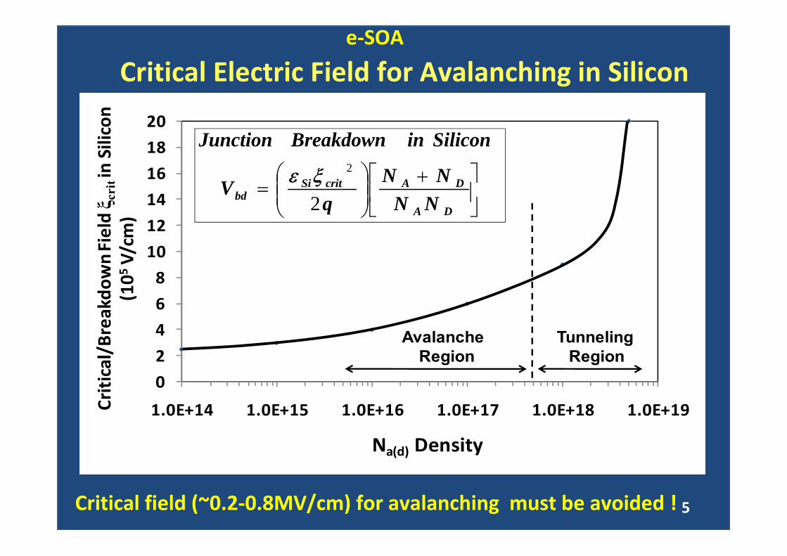
e‐SOA
Critical field (~0.2‐0.8MV/cm) for avalanching must be avoided !
Critical Electric Field for Avalanching in Silicon
5
0
10
20
30
40
50
60
70
80
‐5.0 ‐4.0 ‐3.0 ‐2.0 ‐1.0 0.0 1.0 2.0 3.0 4.0 5.0
N+
ND = NA =
Distance from Metallurgical Junction (μm)
Pote
ntia
l (V)
(5x10¹⁵/cm3) (5x10¹⁵/cm3)
N-TypeP-Type + + + ++ + + +
+ + + ++ + + +
- - - -- - - -
- - - -- - - -
- -- -
++
WVbd=120V
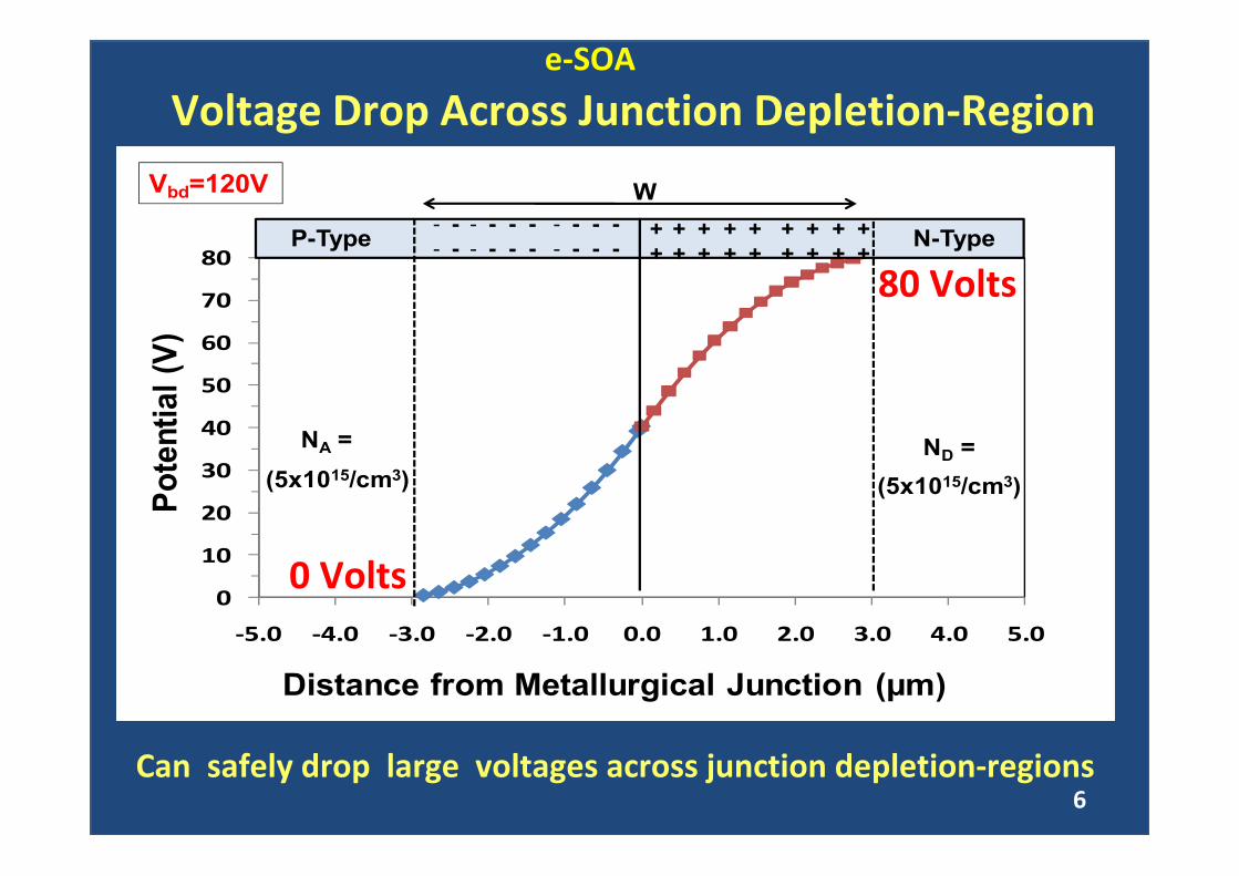
e‐SOA
Can safely drop large voltages across junction depletion‐regions
Voltage Drop Across Junction Depletion‐Region
80 Volts
0 Volts
6
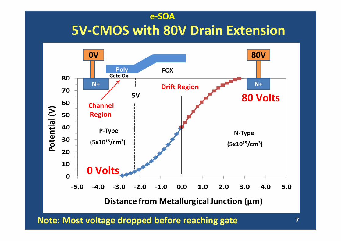
0
10
20
30
40
50
60
70
80
‐5.0 ‐4.0 ‐3.0 ‐2.0 ‐1.0 0.0 1.0 2.0 3.0 4.0 5.0
N+
N‐TypeP‐Type
Distance from Metallurgical Junction (μm)
Potential (V)
(5x10¹⁵/cm3) (5x10¹⁵/cm3)
Poly
N+ N+
FOX
5V
80V0V
Drift Region
ChannelRegion
Gate Ox
e‐SOA
80 Volts
0 Volts
5V‐CMOS with 80V Drain Extension
7Note: Most voltage dropped before reaching gate
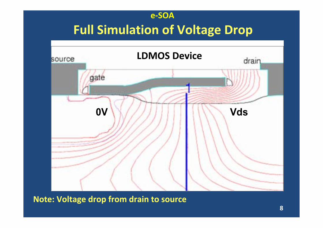
Vds0V
e‐SOA
LDMOS Device
Full Simulation of Voltage Drop
Note: Voltage drop from drain to source8
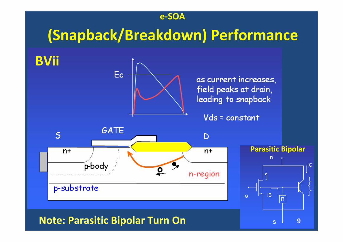
e‐SOA
(Snapback/Breakdown) Performance
Parasitic Bipolar
Note: Parasitic Bipolar Turn On
BVii
9
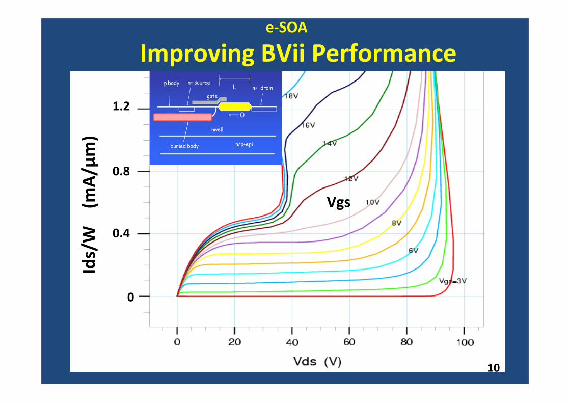
e‐SOA
Improving BVii Performance
0
0.4
0.8
1.2Ids/W (m
A/μm)
Vgs
10
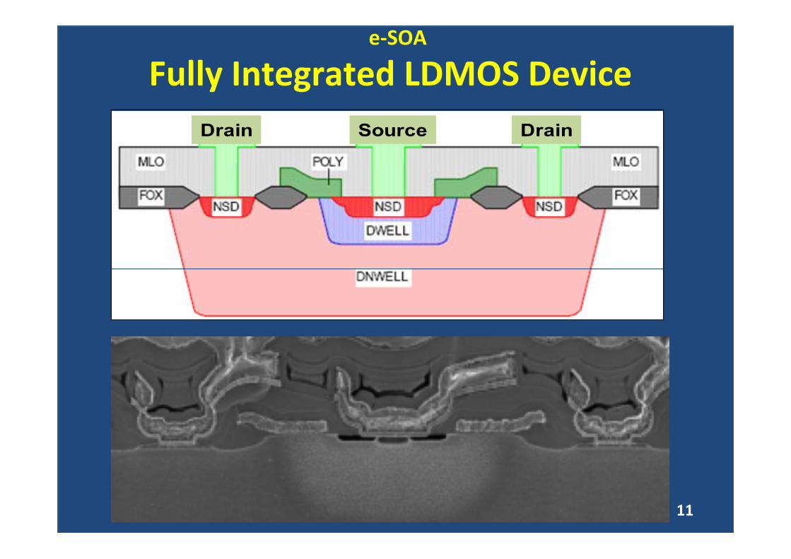
SourceDrain Drain
Fully Integrated LDMOS Devicee‐SOA
11
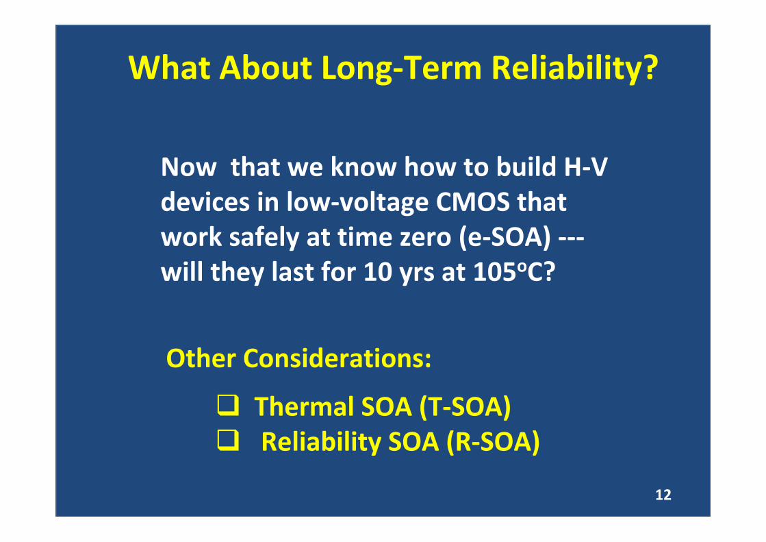
Now that we know how to build H‐V devices in low‐voltage CMOS that work safely at time zero (e‐SOA) ‐‐‐will they last for 10 yrs at 105oC?
What About Long‐Term Reliability?
Thermal SOA (T‐SOA)Reliability SOA (R‐SOA)
Other Considerations:
12
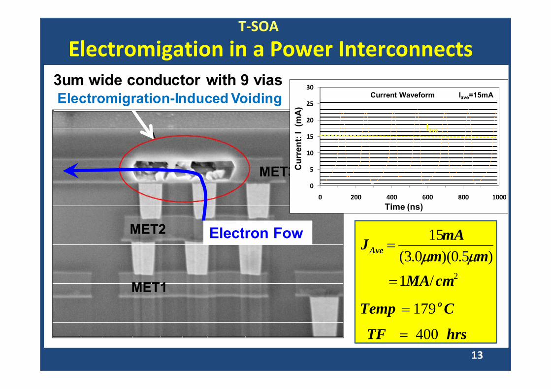
Electron Fow
MET3
MET2
MET1
0
5
10
15
20
25
30
0 200 400 600 800 1000
Time (ns)
Current Waveform
Cur
rent
: I (
mA
)
Iave=15mA
Iave
Electromigration-Induced Voiding
2/1)5.0)(0.3(
15
cmMAmm
mAJAve
=
=μμ
CTemp o179=
hrsTF 400=
3um wide conductor with 9 vias
Electromigation in a Power InterconnectsT‐SOA
13
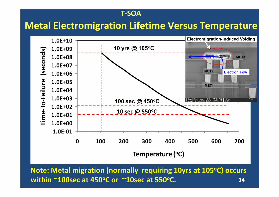
1.0E‐011.0E+001.0E+011.0E+021.0E+031.0E+041.0E+051.0E+061.0E+071.0E+081.0E+091.0E+10
0 100 200 300 400 500 600 700
Time‐To‐Failure (second
s)
Temperature (oC)
10 yrs @ 105oC
100 sec @ 450oC
Note: Metal migration (normally requiring 10yrs at 105oC) occurs within ~100sec at 450oC or ~10sec at 550oC.
Metal Electromigration Lifetime Versus TemperatureT‐SOA
Electron Fow
MET3
MET2
MET1
Electromigration-Induced Voiding
10 sec @ 550oC
14
44
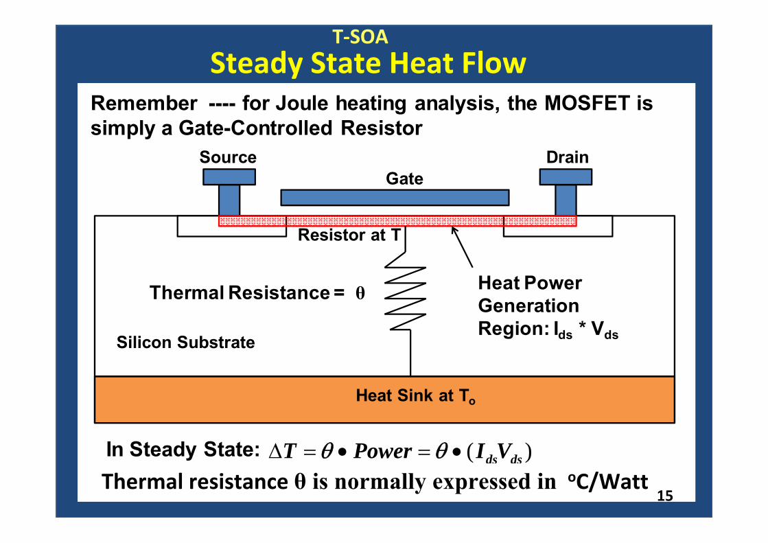
Remember ---- for Joule heating analysis, the MOSFET is simply a Gate-Controlled Resistor
Source DrainGate
Silicon Substrate
Heat Sink at To
Heat PowerGenerationRegion: Ids * Vds
Thermal Resistance = θ
In Steady State: )( dsdsVIPowerT •=•=Δ θθThermal resistance θ is normally expressed in oC/Watt
Resistor at T
Steady State Heat FlowT‐SOA
Thermal resistance θ is normally expressed in oC/Watt15
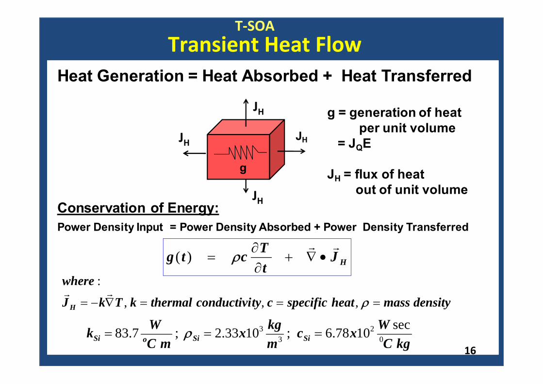
Transient Heat FlowT‐SOA
g
JH
Conservation of Energy:Power Density Input = Power Density Absorbed + Power Density Transferred
HJtTctg
rr•∇+
∂∂
= ρ)(
g = generation of heatper unit volume
= JQE
JH = flux of heat out of unit volume
Heat Generation = Heat Absorbed + Heat Transferred
densitymassheatspecificctyconductivithermalkTkJ
where
H ===∇−= ρ,,,
:rr
kgCWxc
mkgx
mCWk SiSioSi 0
23
3 sec1078.6;1033.2;7.83 === ρ
JH
JH
JH
16
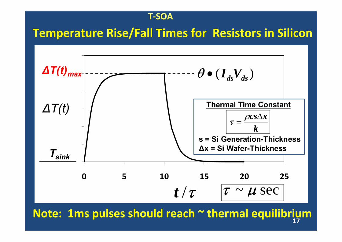
Temperature Rise/Fall Times for Resistors in SiliconT‐SOA
Note: 1ms pulses should reach ~ thermal equilibrium
0
0.2
0.4
0.6
0.8
1
1.2
0 5 10 15 20 25
ΔT(t)
τ/t
)( dsdsVI•θ
0
ΔT(t)max
Tsink
sec~ μτ
kxcsΔ
=ρτ
Thermal Time Constant
s = Si Generation-ThicknessΔx = Si Wafer-Thickness
17
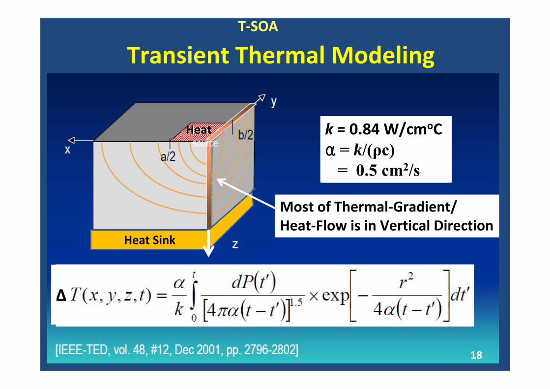
T‐SOA
Transient Thermal Modeling
Heat Sink
Δ
k = 0.84 W/cmoC α = k/(ρc)
= 0.5 cm2/s
Most of Thermal‐Gradient/Heat‐Flow is in Vertical Direction
Heat
18
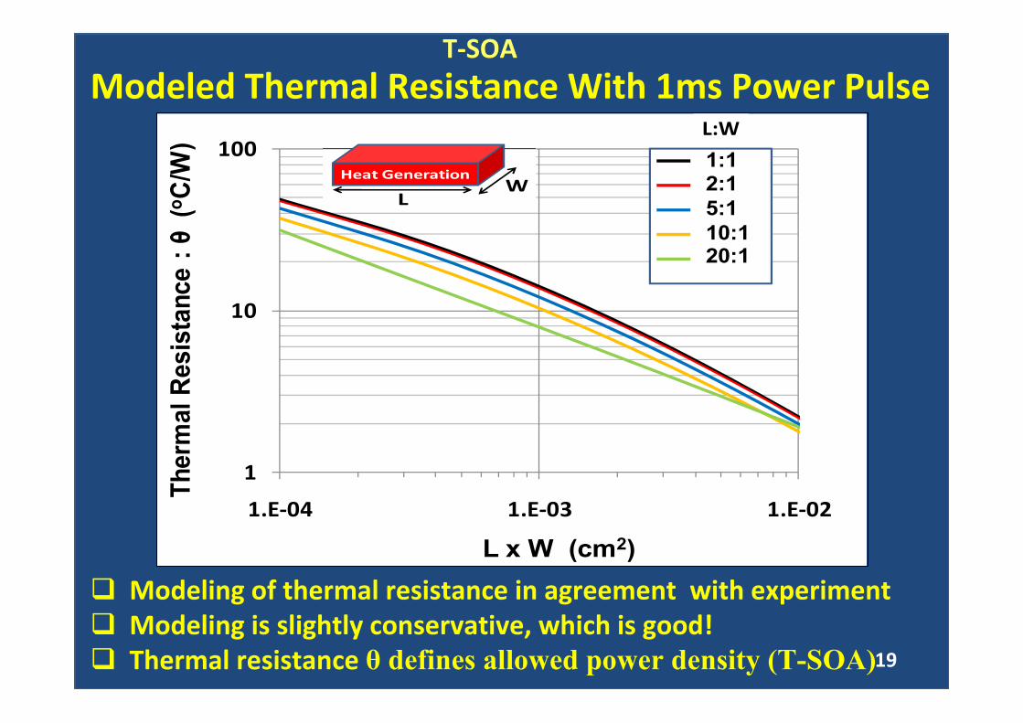
Modeled Thermal Resistance With 1ms Power PulseT‐SOA
1
10
100
1.E‐04 1.E‐03 1.E‐02
L x W (cm2)
Ther
mal
Res
ista
nce
: θ(o C
/W)
1:12:15:110:120:1
W:L
Heat Generation
LW
L:W
Modeling of thermal resistance in agreement with experiment Modeling is slightly conservative, which is good!Thermal resistance θ defines allowed power density (T-SOA)19
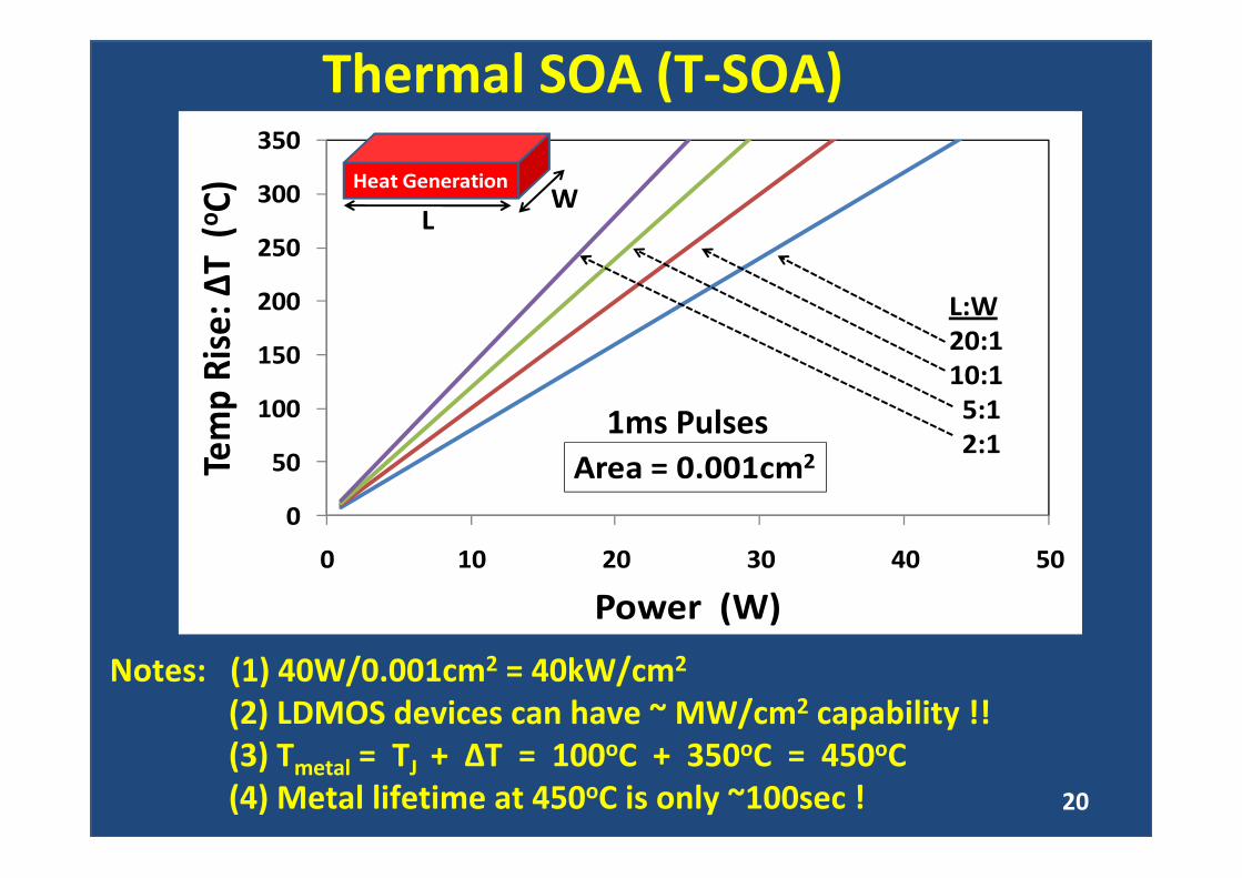
0
50
100
150
200
250
300
350
0 10 20 30 40 50
Power (W)
Temp Rise: Δ
T (oC)
Heat Generation
LW
L:W20:110:15:12:1
Area = 0.001cm2
Thermal SOA (T‐SOA)
Notes: (1) 40W/0.001cm2 = 40kW/cm2
(2) LDMOS devices can have ~ MW/cm2 capability !! (3) Tmetal = TJ + ΔT = 100oC + 350oC = 450oC(4) Metal lifetime at 450oC is only ~100sec !
1ms Pulses
20
R‐SOA
We have learned how to generate: electrical safe operating areas (e‐SOAs)
We have learned how to generate:Thermal safe operating areas: T‐SOAs
What About Long‐Term Reliability?
Hot Carrier Injection (HCI)Biased Temperature Instability (BTI)Time‐Dependent Dielectric Breakdown (TDDB)
Remaining ‐‐‐ Long Term (10yr/105oC) Reliability Safe Operating Areas: R‐SOAs
Thus far ‐‐‐‐
Examples:
21
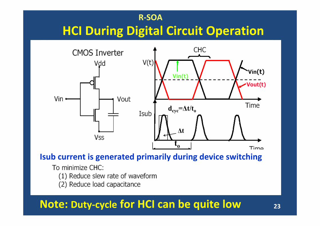
R‐SOA
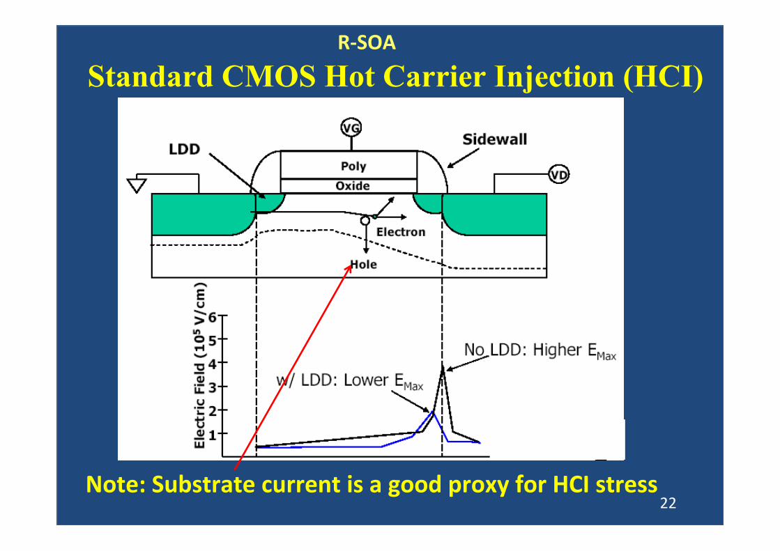
Standard CMOS Hot Carrier Injection (HCI)
22Note: Substrate current is a good proxy for HCI stress
23
to
Δt
dcyc=Δt/to
HCI During Digital Circuit OperationR‐SOA
Note: Duty‐cycle for HCI can be quite low 23
Isub current is generated primarily during device switching
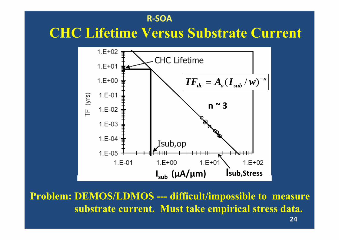
n ~ 3
nsubodc wIATF −= )/(
CHC Lifetime Versus Substrate Current
Isub (μA/μm)
R‐SOA
Problem: DEMOS/LDMOS --- difficult/impossible to measuresubstrate current. Must take empirical stress data.
Isub,Stress
24
0.600 0.200 0.040 5.0
0.030 0.007 0.001 4.0
0.500 0.100 0.030 2.5
1.500 0.500 0.100 1.0
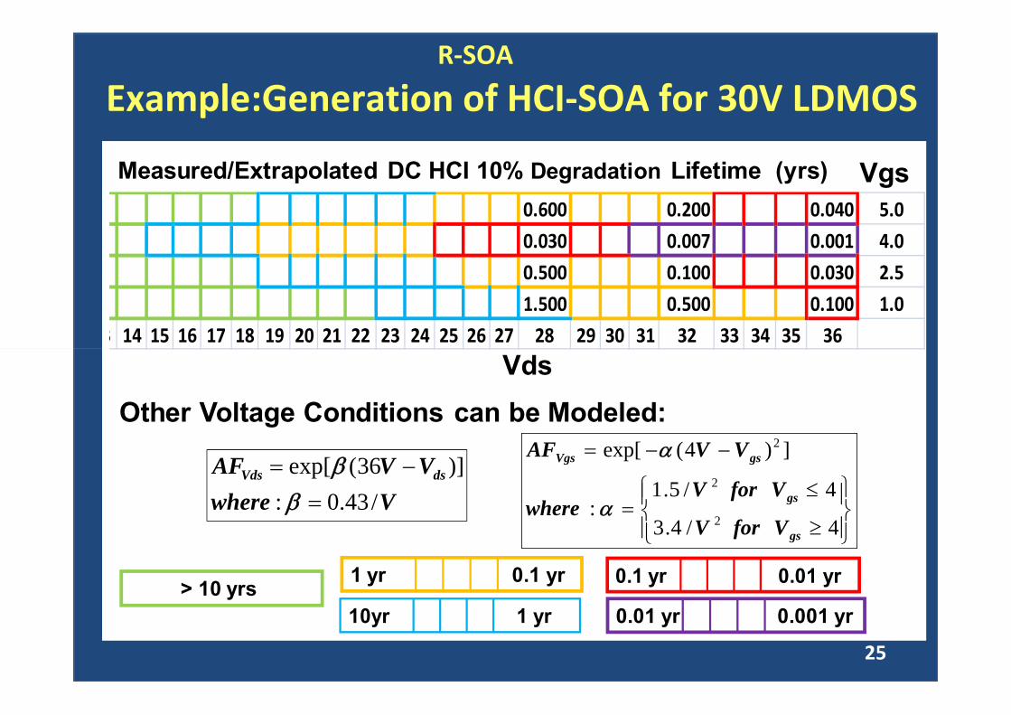
3 14 15 16 17 18 19 20 21 22 23 24 25 26 27 28 29 30 31 32 33 34 35 36
Vgs
Vds
Measured/Extrapolated DC HCI 10% Degradation Lifetime (yrs)
VwhereVVAF dsVds
/43.0:)]36(exp[
=−=
ββ
Other Voltage Conditions can be Modeled:
⎪⎭
⎪⎬⎫
⎪⎩
⎪⎨⎧
≥
≤=
−−=
4/4.3
4/5.1:
])4(exp[
2
2
2
gs
gs
gsVgs
VforV
VforVwhere
VVAF
α
α
> 10 yrs 1 yr 0.1 yr
10yr 1 yr
0.1 yr 0.01 yr
0.01 yr 0.001 yr
Example:Generation of HCI‐SOA for 30V LDMOSR‐SOA
25
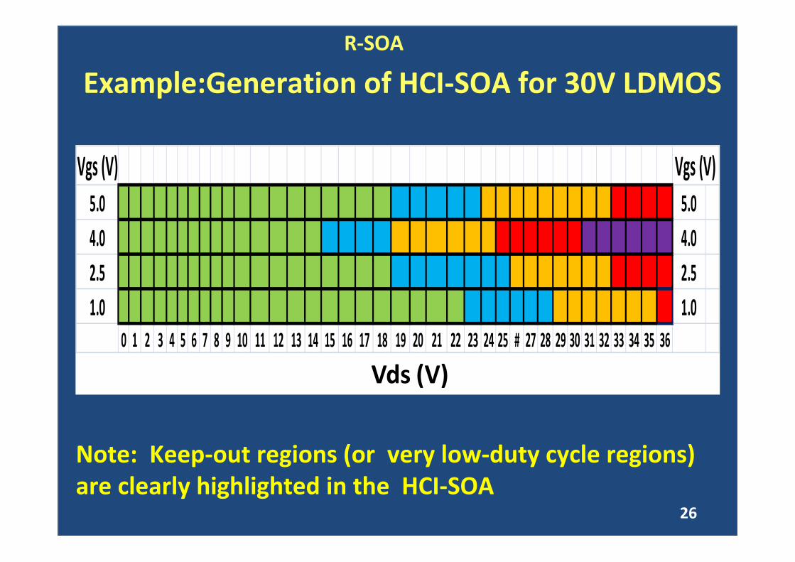
Vgs (V) Vgs (V)5.0 5.04.0 4.02.5 2.51.0 1.0
0 1 2 3 4 5 6 7 8 9 10 11 12 13 14 15 16 17 18 19 20 21 22 23 24 25 # 27 28 29 30 31 32 33 34 35 36
Vds (V)
Example:Generation of HCI‐SOA for 30V LDMOS
Note: Keep‐out regions (or very low‐duty cycle regions) are clearly highlighted in the HCI‐SOA
R‐SOA
26
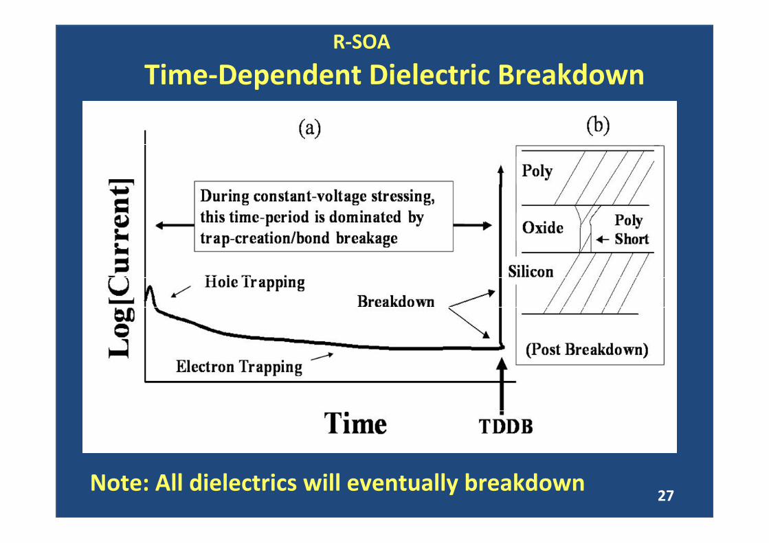
Time‐Dependent Dielectric BreakdownR‐SOA
Note: All dielectrics will eventually breakdown 27
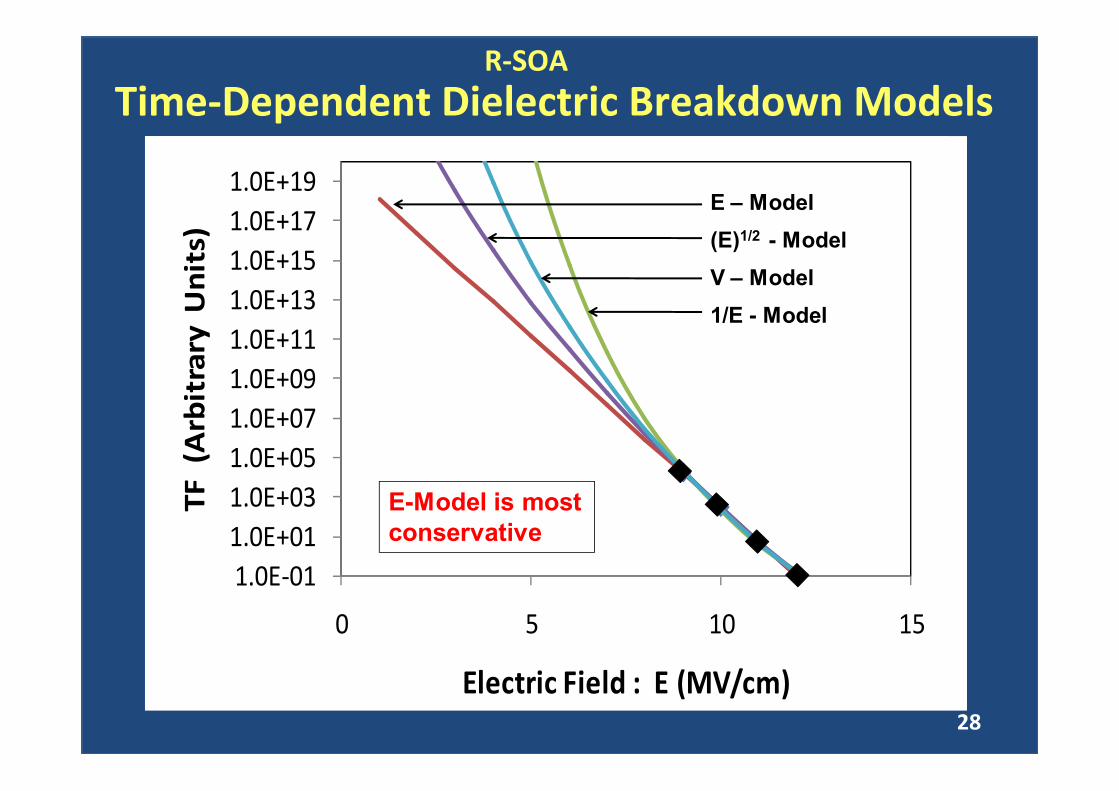
R‐SOATime‐Dependent Dielectric Breakdown Models
1.0E‐011.0E+011.0E+031.0E+051.0E+071.0E+091.0E+111.0E+131.0E+151.0E+171.0E+19
0 5 10 15
TF (Arbitrary Units)
Electric Field : E (MV/cm)
E – Model(E)1/2 - ModelV – Model1/E - Model
E-Model is mostconservative
28
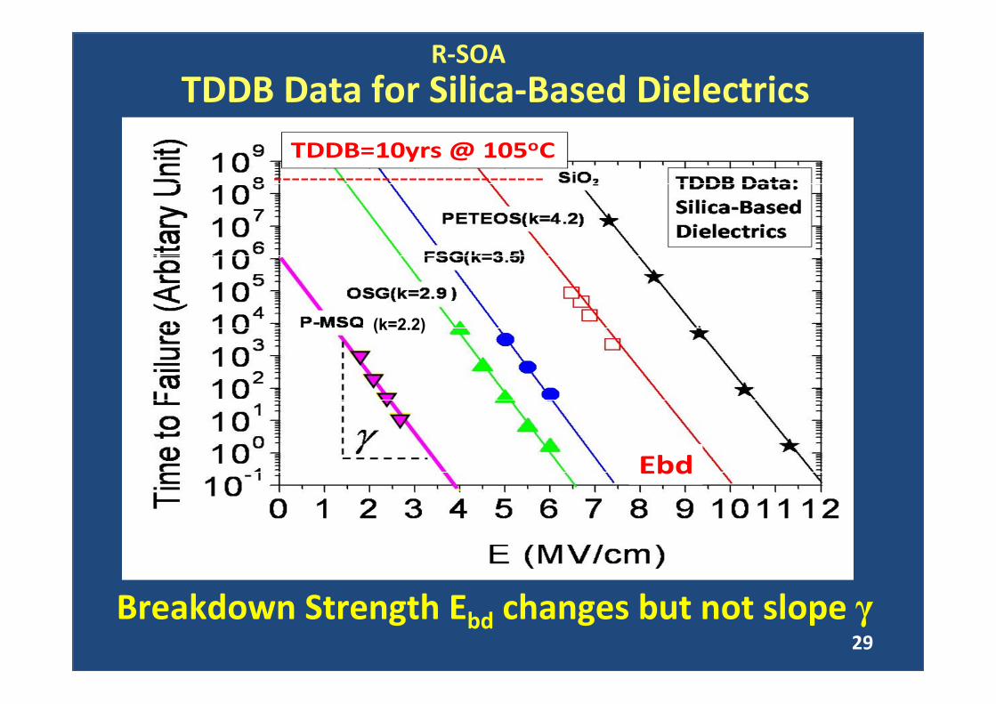
TDDB=10yrs @ 105oC
Ebd
TDDB Data for Silica‐Based DielectricsR‐SOA
Breakdown Strength Ebd changes but not slope γ29
(k=2.2)
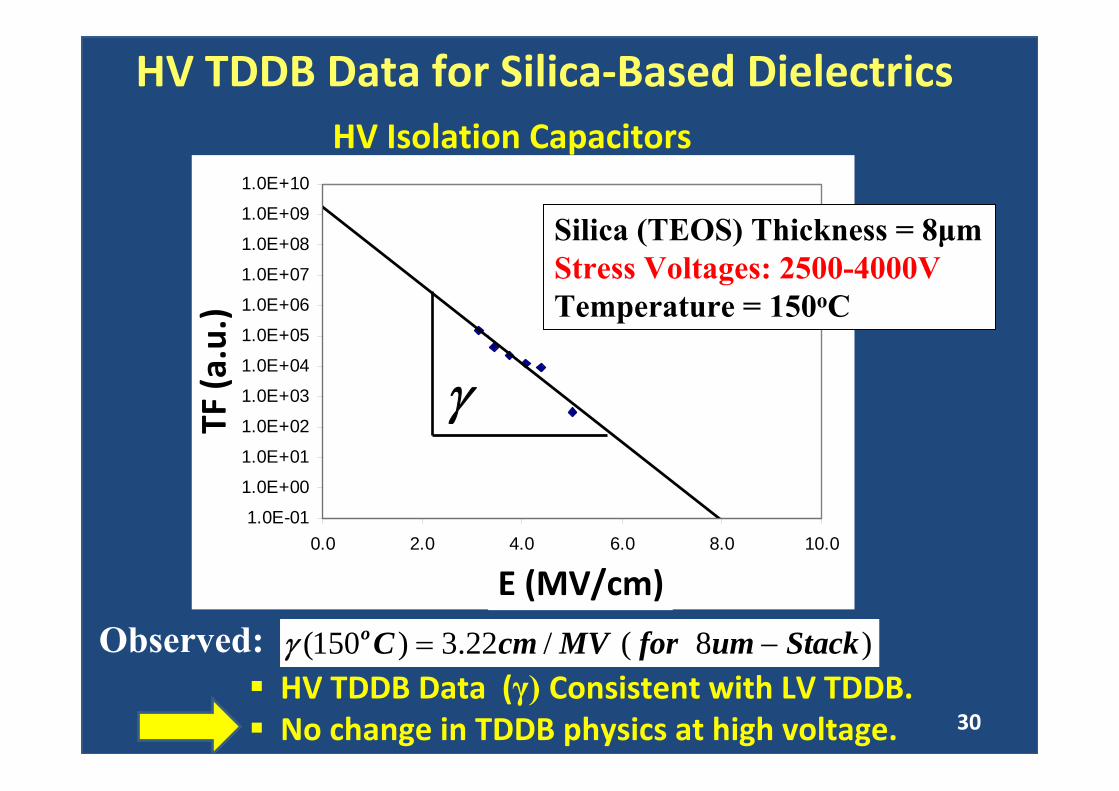
HV TDDB Data for Silica‐Based DielectricsHV Isolation Capacitors
1.0E-01
1.0E+00
1.0E+01
1.0E+02
1.0E+03
1.0E+04
1.0E+05
1.0E+06
1.0E+07
1.0E+08
1.0E+09
1.0E+10
0.0 2.0 4.0 6.0 8.0 10.0
E (MV/cm)
TF (
sec)
)8(/22.3)150( StackumforMVcmCo −=γ
Silica (TEOS) Thickness = 8μmStress Voltages: 2500-4000VTemperature = 150oC
Observed:
γ
HV TDDB Data (γ) Consistent with LV TDDB.No change in TDDB physics at high voltage.
E (MV/cm)
TF (a
.u.)
30
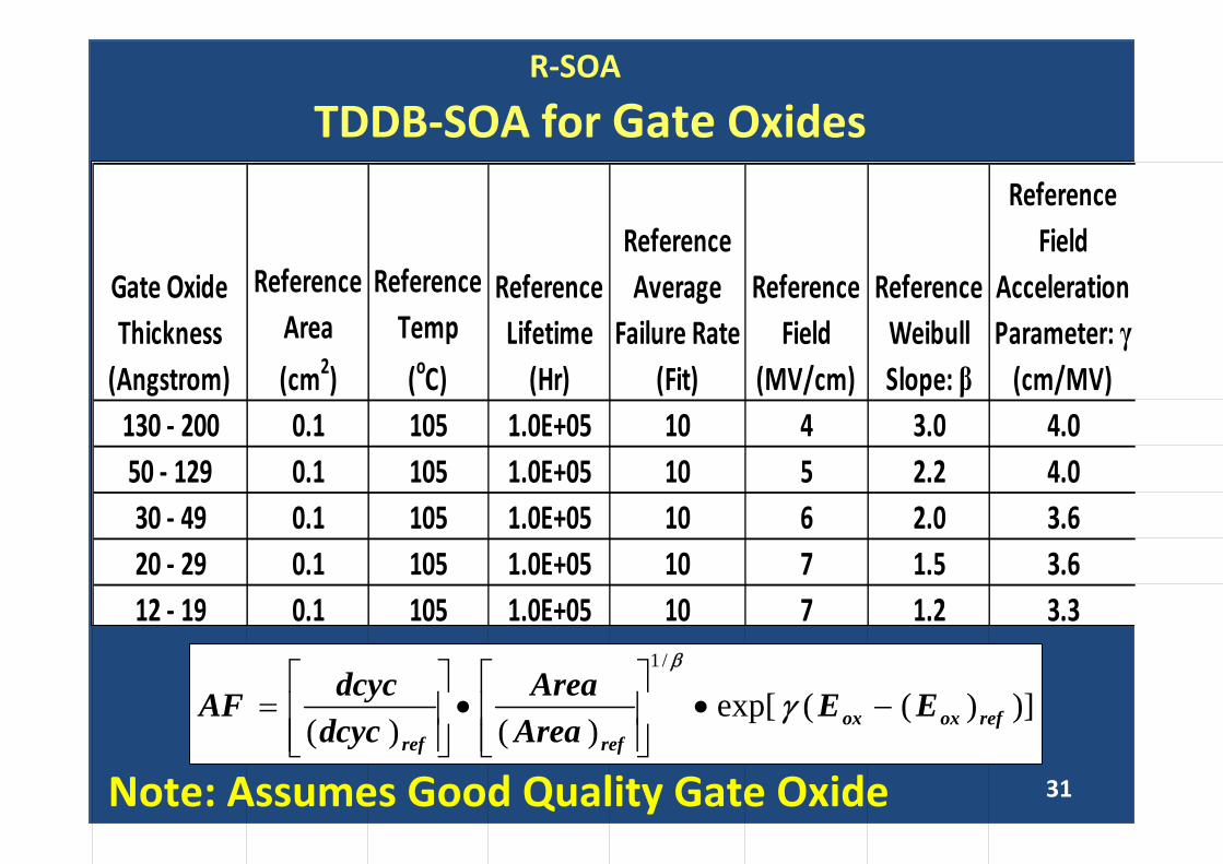
Gate Oxide Thickness (Angstrom)
Reference Area
(cm2)
Reference Temp
(oC)
Reference Lifetime (Hr)
Reference Average
Failure Rate (Fit)
Reference Field
(MV/cm)
Reference Weibull Slope: β
Reference Field
Acceleration Parameter: γ (cm/MV)
130 ‐ 200 0.1 105 1.0E+05 10 4 3.0 4.050 ‐ 129 0.1 105 1.0E+05 10 5 2.2 4.030 ‐ 49 0.1 105 1.0E+05 10 6 2.0 3.620 ‐ 29 0.1 105 1.0E+05 10 7 1.5 3.612 ‐ 19 0.1 105 1.0E+05 10 7 1.2 3.3
TDDB‐SOA for Gate Oxides
Note: Assumes Good Quality Gate Oxide
R‐SOA
31
)])((exp[)()(
/1
refoxoxrefref
EEAreaArea
dcycdcycAF −•
⎥⎥⎦
⎤
⎢⎢⎣
⎡•
⎥⎥⎦
⎤
⎢⎢⎣
⎡= γ
β
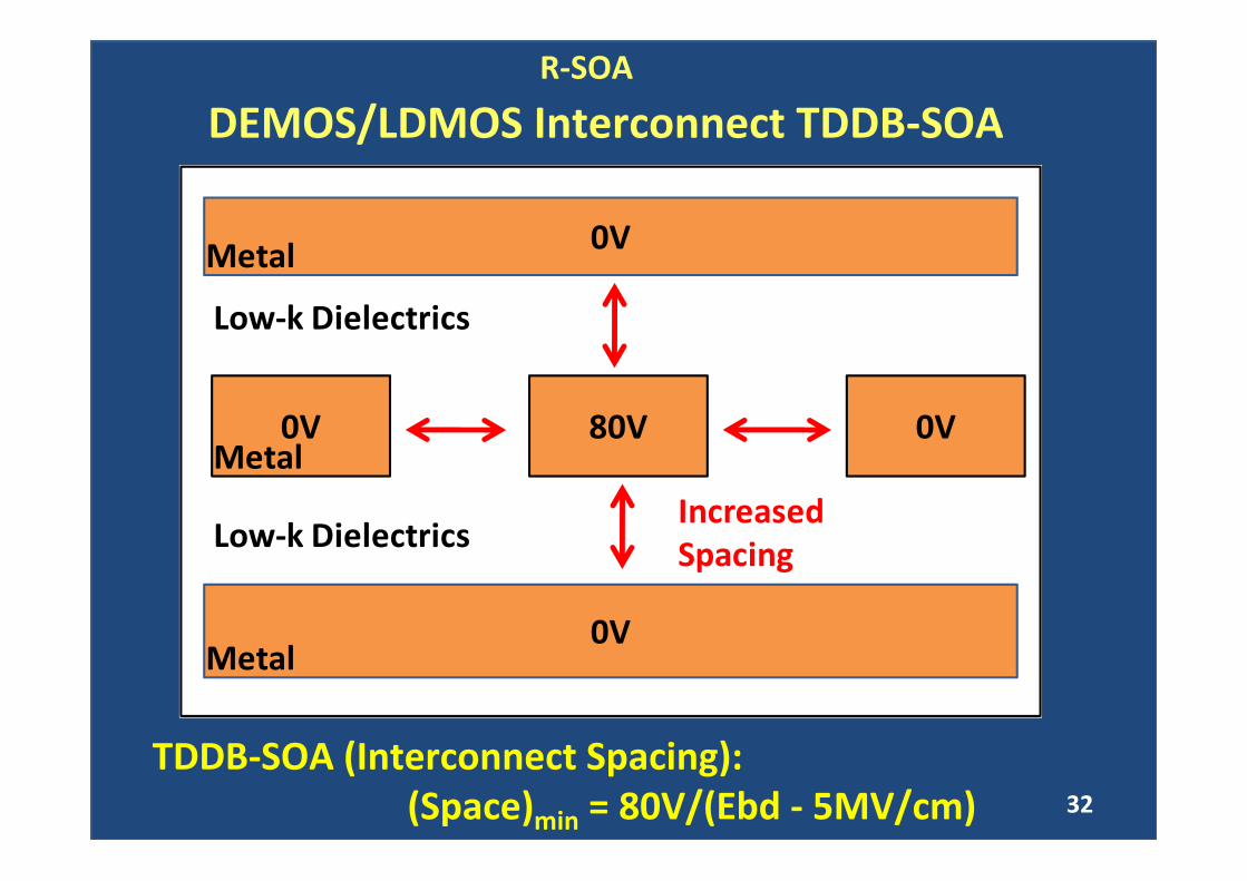
80V 0V
0V
0V
0V
Low‐k Dielectrics
Low‐k DielectricsIncreasedSpacing
Metal
Metal
Metal
DEMOS/LDMOS Interconnect TDDB‐SOA R‐SOA
TDDB‐SOA (Interconnect Spacing): (Space)min = 80V/(Ebd ‐ 5MV/cm) 32
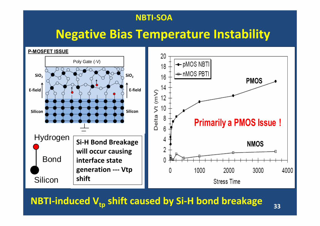
E‐fieldE‐field
Silicon Silicon
SiO2 SiO2
Poly Gate (-V)
P-MOSFET ISSUE
Primarily a PMOS Issue !
NMOS
PMOS
Silicon
Hydrogen
Bond
NBTI‐SOA
Negative Bias Temperature Instability
Si‐H Bond Breakage will occur causing interface state generation ‐‐‐ Vtp shift
NBTI‐induced Vtp shift caused by Si‐H bond breakage 33
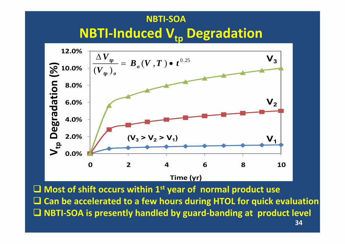
0.0%
2.0%
4.0%
6.0%
8.0%
10.0%
12.0%
0 2 4 6 8 10
Parameter Degrada
tion (%)
Time (yr)
25.0),()(
tTVBV
Vo
otp
tp •=Δ
V1
V2
V3
(V3 > V2 > V1)
NBTI‐Induced Vtp DegradationVtpDegrada
tion
(%)
NBTI‐SOA
Most of shift occurs within 1st year of normal product useCan be accelerated to a few hours during HTOL for quick evaluationNBTI‐SOA is presently handled by guard‐banding at product level
34
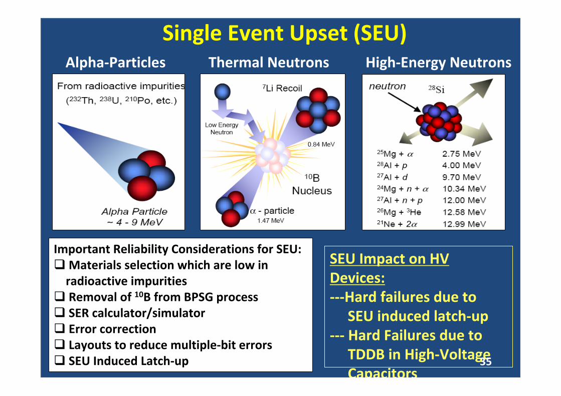
Alpha‐Particles Thermal Neutrons High‐Energy Neutrons
Single Event Upset (SEU)
Important Reliability Considerations for SEU:Materials selection which are low in radioactive impuritiesRemoval of 10B from BPSG process SER calculator/simulatorError correctionLayouts to reduce multiple‐bit errorsSEU Induced Latch‐up
SEU Impact on HV Devices:‐‐‐Hard failures due to
SEU induced latch‐up‐‐‐ Hard Failures due to
TDDB in High‐VoltageCapacitors
35
Conclusions
The business demand for HV components is great
HV components, such as DEMOS and LDMOS devices, can be safely integrated with LV CMOS when careful attention is given to Safe Operating Areas:
‐‐‐ e‐SOA‐‐‐ T‐SOA‐‐‐ R‐SOA
SEU‐induced hard failures will need to be investigated more closely for HV devices
36