Embed Size (px)
Citation preview
Sabine Kob
Positionally AccurateDecoration and Backlighting3-D Capacitive Sensors
11/2012Volume 102 www.kunststoffe-international.com
Magazine for Plastics
SPECIAL3-D PRINTING IS BOOSTING
PRODUCT DEVELOPMENTfrom page 8
PelletizingAdding of Inorganic
Materials as Challenge 22
Fiber CompositesCustomized Thermoset
Matrix Systems 34
© Carl Hanser Verlag, München. 2012. All rights including reprinting, photographic reproduction and
translation reserved by the publishers.
Special reprint from Kunststoffe international 11/2012
Kunststoff Helmbrechts AG Pressecker Str. 39D-95233 HelmbrechtsTel +49-9252-709-0 Fax +49-9252-709-199www.helmbrechts.de
Internet-PDF-Datei. Diese PDF Datei enthält das Recht zur unbeschränkten Intranet- und Internetnutzung, sowie zur Verbreitung über elektronische Verteiler. Eine Verbreitung in gedruckter Form ist mit dieser PDF-Datei nicht gestattet.
2
SURFACE F IN I SH ING
© Carl Hanser Verlag, Munich Kunststoffe international 11/2012
SABINE KOB
How do we imagine that radios, airconditioning or hands-free phonesin car interiors will be operated in
future? Will there still be a plethora ofbuttons press, or will touch-sensitive op-erating concepts prevail here, as withsmartphones or tablet PCs? If the designdepartments of large automotive compa-nies are to be believed, the latter will bethe case – and industry is being asked tocreate the technical prerequisites for this.
The joint development project My-Wave-3D by Kunststoff Helmbrechts AG(KH), Helmbrechts, Germany, andMID-Tronic Wiesauplast GmbH, Wies-au, Germany, is now completing an im-portant technology step and permittingtouch-sensitive operation by means ofcapacitive fields on a three-dimension-ally shaped, decorated and backlit sur-face.
At the core is the combination of acurved injection molded part that is dec-
orated by in-mold labeling (IML), and a3-D circuit board conforming to the partcontour, which is populated with elec-tronic parts by a newly developed 3-D au-tomatic SMT placement unit. The newconcept thus meets considerable de-mands, which users are familiar withfrom car interior design – high-qualitysurfaces with printed operating symbolsand backlighting, permitting a day andnight effect.
Printing Process Must Allow forthe Subsequent Deformation
The surface technology was the respon-sibility of KH, with its IML-specializedsubsidiary Foliotec GmbH, Sparneck,Germany, which produces the operatingelement in three versions: with high-glossblack and scratchproof coated, matt-black or transparent surface. For the blackvariants, a 250 µm-thick PC film is mul-ti-pass printed (Fig. 1): two times black, inwhich the first pass precisely defines theoutlines of text and symbols, and the sec-ond is opaque to deepen the black andprevent so-called “flashes,”i.e. gaps in theprinted area.
The black layers have a double whitebacking to make the symbols visible. Toachieve a black-panel or disappearanceeffect in the upper region of the part, twoblack translucent layers are printed – thenthe IML film is coated overall with clearlacquer. In the positioning of the symbols,the subsequent deformation (18 mmconvex, edge radius 1 mm) must be tak-en into account so that afterwards every-thing is in the right place. After formingof the heated film with over 100 bar com-pressed air, the scratchproof coating of
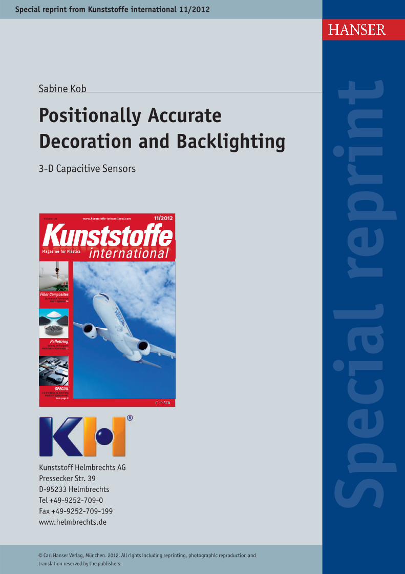
3-D Capacitive Sensors. A
glimpse into the car interior of
tomorrow? The MyWave-3D
development project presents
touch-sensitive operation by
means of capacitive fields on a
convex, IML-decorated and
backlit surface. This is made
possible by means of a novel
circuit board conforming to the
part geometry and populated in
3-D.
Positionally AccurateDecoration and Backlighting
At the core of the MyWave-3D is the combination of a curved injection molded part that is decorated by in-moldlabeling (IML), and a 3-D circuit board con-forming to the part contour (photos: KH)
Kunststoff Helmbrechts AGD-95233 HelmbrechtsGermanyTEL +49 9252 709-0> www.helmbrechts.de
MID-Tronic Wiesauplast GmbHD-95676 WiesauGermanyTEL +49 9634 88-820> www.mid-tronic.de
Contacti
Translated from Kunststoffe 11/2012, pp. 31–33Article as PDF-File at www.kunststoffe-international.com; Document Number: PE111193
Internet-PDF-Datei. Diese PDF Datei enthält das Recht zur unbeschränkten Intranet- und Internetnutzung, sowie zur Verbreitung über elektronische Verteiler. Eine Verbreitung in gedruckter Form ist mit dieser PDF-Datei nicht gestattet.
3
SURFACE F IN I SH ING
Kunststoffe international 11/2012 www.kunststoffe-international.com
the black high-gloss MyWave version iscured under UV light. Following stamp-ing and insertion into the mold, the filmblank is backmolded with PC.
LDS of the Circuit Board
The novel 3-D circuit board with the elec-tronic components comes from the part-ner MID-Tronic. It is provided with con-ductor tracks, capacitive surface andshielding by LDS (laser direct structur-ing) (Fig. 2). The circuit board is producedfrom a polymer, which contains additivesand is activated by laser at precisely de-fined points. The bond between the poly-mer and additives ruptures here, and the
above-mentioned conductive tracks andsurfaces are produced from the now-ex-posed copper ions, in a multistageprocess.
The part is populated with electroniccomponents by an own-developed SMTplacement unit with a six-axis robot. Op-erating at up to 1 m/s with a positioningaccuracy of ±0.05 mm, it applies LEDs,resistors, capacitors and other electroniccomponents. It can act at a deformationheight of up to 50 mm, while convention-al placement units are limited to 20 mm.Another advantage is the angle-true pop-ulation through oblique positioning ofthe workpiece. For example the lightingeffect of LEDs can be precisely controlledand optimally utilized. The soldering ofparts then takes place by a vapor phaseprocess, which achieves a uniform tem-perature profile throughout, including oncurved surfaces.
The 3-D circuit board contains thefunctional electronics but not the controlelectronics. In automotive engineering, itis always installed in a central control unitand thus contains essential know-how ofthe OEM. In addition, money can besaved and the overall height reduced.LDS, as a multi-stage manufacturing
process, is more expensive than the pro-duction of conventional flat circuitboards, and the latter also offer morespace for applying conductive tracks: upto 100 layers can be accommodated on1.5 mm thickness. For future series appli-cations, therefore, the dictum is: as muchperipheral electronics as necessary (con-signed to modules and circuit boards withpleasantly tactile shapes) – as much cen-tralized electronics on flat circuit boardsas possible.
One Microprocessor for ThreeOperating Modes
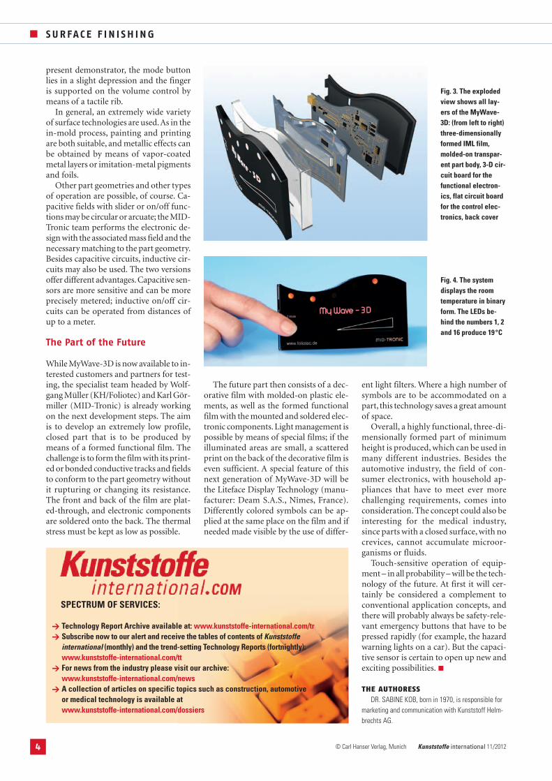
To allow the MyWave-3D Demonstratorto show what it can do, however, it wasnecessary to integrate a flat control cir-cuit board with microprocessor into thepart (Fig. 3), by means of which three dif-ferent operating modes can be chosen.Immediately after it is switched on by agentle touch of the power button, the sys-tem displays the room temperature in bi-nary form. That means the LEDs behindthe numbers 1, 2 and 16 produce 19°C(Fig. 4). For the numbers, the KH/Foliotecteam realized an effective disappearanceeffect (also known as black panel effect).
They are almost invisible when notswitched on.
Tapping again on the mode button ac-tivates an infinitely variable color change.Behind the MyWave-3D is an opticalwaveguide with scattering pigments thatis formed for a correctly angled illumina-tion similar to the part surfaces, RGBLEDs are mounted next to it. These red-green-blue LEDs can show all the colorsof the rainbow. If you stroke your fingerlightly over the volume controller print-ed on the part surface, the text changescolor.When you have reached the desiredcolor, you take your finger away and thecolor remains. The capacitive field can beadjusted so that it is not necessary totouch the plastic surface,but only to movethe finger at a slight distance from it.
The third mode, via the volume con-trol, sets off a curved row of LEDs on theupper edge of the operating element, witha long row for high volume and a shortrow for low volume. For control, it is pos-sible to stroke along the volume controlor only to touch it at a point. The runningLEDs change depending on the fingermovement.
Various Design Possibilities
As regards the decoration and backlight-ing possibilities,MyWave-3D already goeswell beyond other concepts, which so farhave only presented a three-dimensionalcapacitive monochrome surface. The ap-plication of control symbols is of funda-mental importance for the operation ofhousehold appliances or equipment inauto cockpits. Sensory feedback, whichone receives routinely at present whenpressing keys or turning knobs, can be ob-tained acoustically when operating capac-itive surfaces; in addition, raised or de-pressed tactile aids can be used. With the
Fig. 1. In the cylinder printing machine, the MyWave-3D is decorated in a total of seven screen print-ing runs
Fig. 2. The novel 3-Dcircuit board is pro-vided with conductortracks, capacitivesurface (jagged re-gion on the circuitboard) and shielding(surrounding meshsurface)
Internet-PDF-Datei. Diese PDF Datei enthält das Recht zur unbeschränkten Intranet- und Internetnutzung, sowie zur Verbreitung über elektronische Verteiler. Eine Verbreitung in gedruckter Form ist mit dieser PDF-Datei nicht gestattet.
4
SURFACE F IN I SH ING
© Carl Hanser Verlag, Munich Kunststoffe international 11/2012
present demonstrator, the mode buttonlies in a slight depression and the fingeris supported on the volume control bymeans of a tactile rib.
In general, an extremely wide varietyof surface technologies are used.As in thein-mold process, painting and printingare both suitable, and metallic effects canbe obtained by means of vapor-coatedmetal layers or imitation-metal pigmentsand foils.
Other part geometries and other typesof operation are possible, of course. Ca-pacitive fields with slider or on/off func-tions may be circular or arcuate; the MID-Tronic team performs the electronic de-sign with the associated mass field and thenecessary matching to the part geometry.Besides capacitive circuits, inductive cir-cuits may also be used. The two versionsoffer different advantages. Capacitive sen-sors are more sensitive and can be moreprecisely metered; inductive on/off cir-cuits can be operated from distances ofup to a meter.
The Part of the Future
While MyWave-3D is now available to in-terested customers and partners for test-ing, the specialist team headed by Wolf-gang Müller (KH/Foliotec) and Karl Gör-miller (MID-Tronic) is already workingon the next development steps. The aimis to develop an extremely low profile,closed part that is to be produced bymeans of a formed functional film. Thechallenge is to form the film with its print-ed or bonded conductive tracks and fieldsto conform to the part geometry withoutit rupturing or changing its resistance.The front and back of the film are plat-ed-through, and electronic componentsare soldered onto the back. The thermalstress must be kept as low as possible.
The future part then consists of a dec-orative film with molded-on plastic ele-ments, as well as the formed functionalfilm with the mounted and soldered elec-tronic components. Light management ispossible by means of special films; if theilluminated areas are small, a scatteredprint on the back of the decorative film iseven sufficient. A special feature of thisnext generation of MyWave-3D will bethe Liteface Display Technology (manu-facturer: Deam S.A.S., Nîmes, France).Differently colored symbols can be ap-plied at the same place on the film and ifneeded made visible by the use of differ-
ent light filters. Where a high number ofsymbols are to be accommodated on apart, this technology saves a great amountof space.
Overall, a highly functional, three-di-mensionally formed part of minimumheight is produced, which can be used inmany different industries. Besides theautomotive industry, the field of con-sumer electronics, with household ap-pliances that have to meet ever morechallenging requirements, comes intoconsideration. The concept could also beinteresting for the medical industry,since parts with a closed surface, with nocrevices, cannot accumulate microor-ganisms or fluids.
Touch-sensitive operation of equip-ment – in all probability – will be the tech-nology of the future. At first it will cer-tainly be considered a complement toconventional application concepts, andthere will probably always be safety-rele-vant emergency buttons that have to bepressed rapidly (for example, the hazardwarning lights on a car). But the capaci-tive sensor is certain to open up new andexciting possibilities.�
THE AUTHORESS
DR. SABINE KOB, born in 1970, is responsible formarketing and communication with Kunststoff Helm-brechts AG.
Fig. 3. The explodedview shows all lay-ers of the MyWave-3D: (from left to right)three-dimensionallyformed IML film,molded-on transpar-ent part body, 3-D cir-cuit board for thefunctional electron-ics, flat circuit boardfor the control elec-tronics, back cover
Fig. 4. The systemdisplays the roomtemperature in binaryform. The LEDs be-hind the numbers 1, 2and 16 produce 19°C
SPECTRUM OF SERVICES:
> Technology Report Archive available at: www.kunststoffe-international.com/tr> Subscribe now to our alert and receive the tables of contents of Kunststoffe
international (monthly) and the trend-setting Technology Reports (fortnightly): www.kunststoffe-international.com/tt
> For news from the industry please visit our archive: www.kunststoffe-international.com/news
> A collection of articles on specific topics such as construction, automotive or medical technology is available atwww.kunststoffe-international.com/dossiers
Internet-PDF-Datei. Diese PDF Datei enthält das Recht zur unbeschränkten Intranet- und Internetnutzung, sowie zur Verbreitung über elektronische Verteiler. Eine Verbreitung in gedruckter Form ist mit dieser PDF-Datei nicht gestattet.


![MyWave RM Fact Sheet[1] - bhsaltriskfinancing.com€¦ · MyWave ® Portal Click +Connect +Communicate Welcome to a whole new way of working — MyWave ® is your personalized website](https://img.pdfslide.us/doc/110x75/601f30231de77e2ec04b4a2a/mywave-rm-fact-sheet1-mywave-portal-click-connect-communicate-welcome-to.jpg)